

Approval
TO
DATE :: Nov. 22, 2010
SAMSUNG TFT-LCD
MODEL NO. : LTN156AT15-Cxx
NOTE : Extension code [ - Cxx ]
www.jxlcd.com
www.jxlcd.com
The information described in this SPEC is preliminary and can be changed without prior notice.
Application engineering part, Mobile Division
→ LTN156AT15-Cxx
Surface type [ Glare ]
Samsung Electronics Co., Ltd.
Samsung Secret
Doc.No. Rev.No
04-A00-G-101122
Page
/ 33LTN156AT15-Cxx
1
CONTENTS
Approval
Revision History
General Description
1. Absolute Maximum Ratings
1.1 Absolute Ratings of environment
1.2 Electrical Absolute Ratings
2. Optical Characteristics
3. Electrical Characteristics
3.1 TFT LCD Module
3.2 Backlight Unit
3.3 LED Driver
4. Block Diagram
4.1 TFT LCD Module
4.2 LED Placement Structure
5. Input Terminal Pin Assignment
5.1 Input Signal & Power
5.2 LVDS Interface
5.3 Timing Diagrams of LVDS For Transmitting
www.jxlcd.com
5.4 Input Signals, Basic Display Colors and Gray Scale of Each Color.
www.jxlcd.com
5.5 Pixel format
- - - - - - - - - - - - - - - - - - - ( 3 )
- - - - - - - - - - - - - - - - - - - ( 4 )
- - - - - - - - - - - - - - - - - - - ( 5 )
- - - - - - - - - - - - - - - - - - - ( 7 )
- - - - - - - - - - - - - - - - - - - ( 10 )
- - - - - - - - - - - - - - - - - - - ( 13 )
- - - - - - - - - - - - - - - - - - - ( 14 )
6. Interface Timing
6.1 Timing Parameters
6.2 Timing Diagrams of interface Signal
6.3 Power ON/OFF Sequence
7. Outline Dimension
8. Packing
9. Markings & Others
10. General Precautions
11. EDID
Samsung Secret
Doc.No. Rev.No
- - - - - - - - - - - - - - - - - - - ( 21 )
- - - - - - - - - - - - - - - - - - - ( 24 )
- - - - - - - - - - - - - - - - - - - ( 26 )
- - - - - - - - - - - - - - - - - - - ( 27 )
-- - - - - - - - - - - - - - - - - - ( 29 )
- - - - - - - - - - - - - - - - - -- ( 31 )
04-A00-G-101122
Page
/ 33LTN156AT15-Cxx
2
REVISION HISTORY
Approval
Date Revision No. Page
Nov.22 A00 All The approval specification of LTN156AT15-Cxx was issued first.
Summary
www.jxlcd.com
www.jxlcd.com
Samsung Secret
Doc.No. Rev.No
04-A00-G-101122
Page
/ 33LTN156AT15-Cxx
3
Approval
GENERAL DESCRIPTION
DESCRIPTION
LTN156AT15 is a color active matrix TFT (Thin Film Transistor) liquid crystal display
(LCD) that uses amorphous silicon TFT as switching devices. This model is composed of a
TFT LCD panel, a driver circuit and a backlight unit. The resolution of a 15.6” contains
1366 x 768 pixels and can display up to 262,144 colors. 6 O'clock direction is the optimum
viewing angle.
FEATURES
• High contrast ratio
• HD(1366 x 768 pixels ) resolution
• Low power consumption
• Fast Response
• LED Back Light with embedded LED Driver
• DE (Data enable) only mode
• 3.3V LVDS Interface
• Onboard EEDID chip
APPLICATIONS
• Notebook PC
• If the usage of this product is not for PC application, but for others, please contact SEC
www.jxlcd.com
GENERAL INFORMATION
Display area 344.232 (H) x 193.536 (V) (15.6”diagonal)
Driver element
Display colors
Number of pixel
Pixel arrangement
Pixel pitch 0.252 (H) x 0.252 (V) (TYP.)
www.jxlcd.com
Item Specification Unit Note
mm
a-Si TFT active matrix
262,144
1366 * 768 pixel
RGB vertical stripe
mm
Display Mode
Surface treatment Haze 0, Hardness 3H
Samsung Secret
Doc.No. Rev.No
Normally white
04-A00-G-101122
Page
Glare
/ 33LTN156AT15-Cxx
4
Mechanical Information
Item Min. Typ. Max. Unit Note
Horizontal (H) 358.8 359.3 359.8 mm
Module
size
Note (1) Measurement condition of outline dimension
Vertical (V) 208.95 209.45 209.95 mm
Depth (D) - - 4.0 mm (1)
Weight - 405 420 g
. Equipment : Bernier Calipers
. Push Force : 500g f (minimum)
1. ABSOLUTE MAXIMUM RATINGS
1.1 ENVIRONMENTAL ABSOLUTE RATINGS
Item Symbol Min. Max. Unit Note
Storage temperate TSTG -20 60 C (1)
Approval
Operating temperate
(Temperature of glass surface)
Shock ( non-operating ) Snop - 240 G (2),(4)
Vibration (non-operating) Vnop - 2.41 G (3),(4)
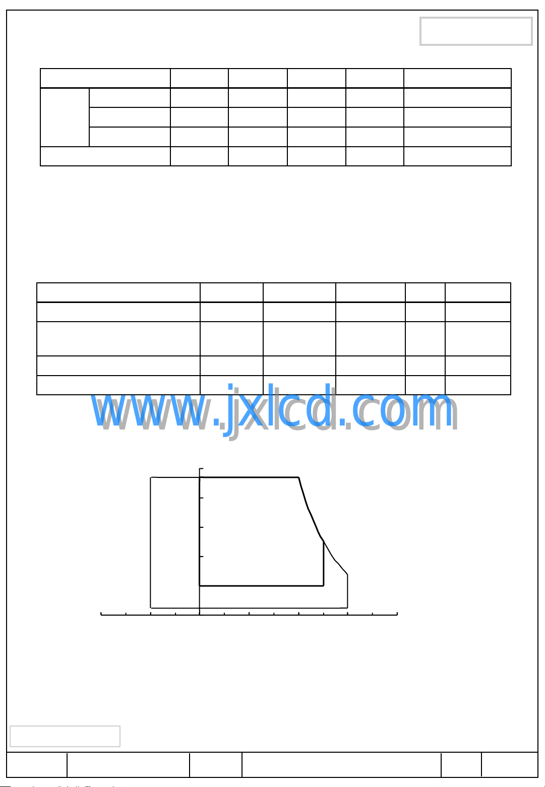
Note (1) Temperature and relative humidity range are shown in the figure below.
95 % RH Max. (40 C Ta)
www.jxlcd.com
www.jxlcd.com
Maximum wet - bulb temperature at 39 OC or less. (Ta 40 C ) No condensation
100
90
80
60
40
20
0
-40 -20 0 20 40 60 80
TOPR 0 50 C (1)
Relative Humidity ( %RH)
( 40,90 )
Operating Range
Storage Range
5
( 50,50.4 )
( 60,27.7 )
Temperature (OC)
(2) 2ms, half sine wave, one time for X, Y, Z.
(3) 5 - 500 Hz, random vibration, 30min for X, Y, Z.
(4) At testing Vibration and Shock, the fixture in holding the Module to be tested have to be
hard and rigid enough so that the Module would not be twisted or bent by the fixture.
Samsung Secret
Doc.No. Rev.No
04-A00-G-101122
Page
/ 33LTN156AT15-Cxx
5
1.2 ELECTRICAL ABSOLUTE RATINGS
(1) TFT LCD MODULE
Item Symbol Min. Max. Unit Note
Power Supply Voltage VDD VDD - 0.3 VDD + 0.3 V (1)
Logic Input Voltage VIN VDD - 0.3 VDD + 0.3 V (1)
Note (1) Within Ta (25 2 C )
Approval
VDD =3.3V, VSS = GND = 0V
www.jxlcd.com
www.jxlcd.com
Samsung Secret
Doc.No. Rev.No
04-A00-G-101122
Page
/ 33LTN156AT15-Cxx
6
Approval
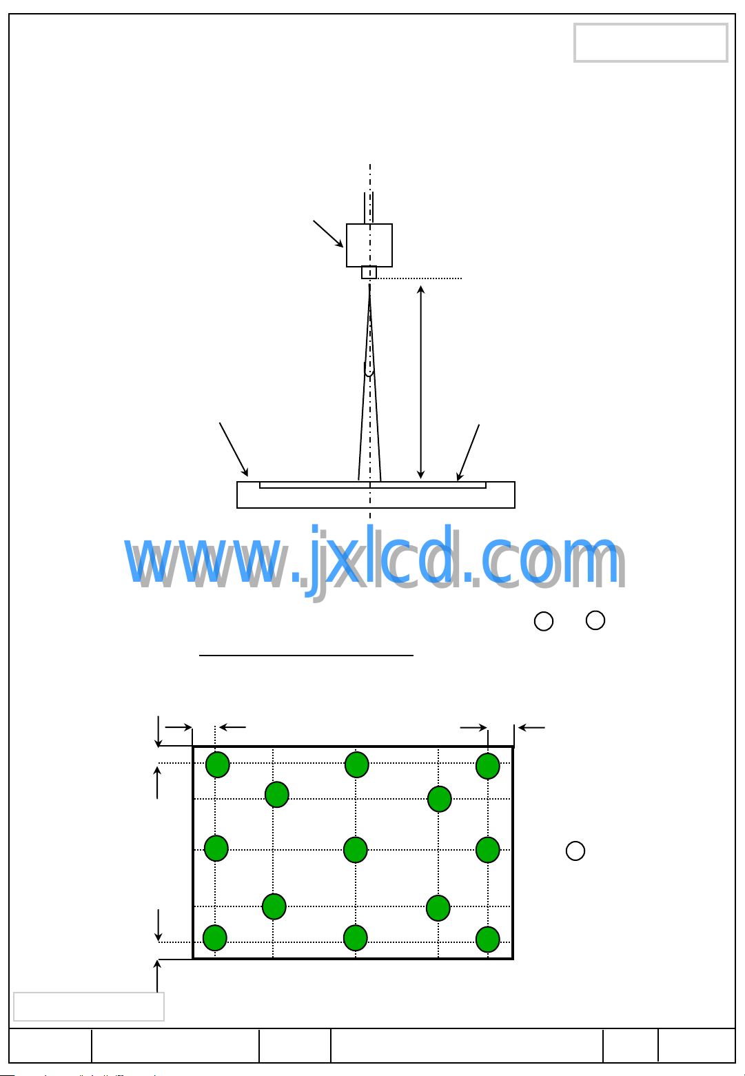
2. OPTICAL CHARACTERISTICS
The following items are measured under stable conditions. The optical characteristics
should be measured in a dark room or equivalent state with the methods shown in Note (5).
Measuring equipment : TOPCON SR-3
* Ta = 25 2 C, VDD=3.3V, fv= 60Hz, fDCLK = 72.33MHz, IF = 100% duty
Item Symbol Condition Min. Typ. Max Unit Note
Contrast Ratio
(5 Points)
Response Time at Ta
( Rising + Falling )
Average Luminance
of White (5 Points)
Red
Green
Color
Chromaticity
( CIE )
www.jxlcd.com
www.jxlcd.com
Blue
CR
TRT - 16 25 msec (1), (3)
YL,AVE 190 220 - cd/m
Normal
RX
RY 0.355
GX 0.355
GY 0.610
BX 0.150
BY 0.100
Viewing
Angle
= 0
= 0
300 500 - - (1), (2), (5)
IF=100%
-0.03
2
0.615
+0.03 -
duty
(1), (4)
(1), (5)
SR-3
WX 0.313
White
WY 0.329
L
Hor.
Viewing
Angle
Ver.
Color Gamut CG - 60 - %
13 Points
White Variation
Samsung Secret
H
H
L
L
CR 10
At center
Doc.No. Rev.No
40 45 -
40 45 -
15 15 -
30 30 -
- - 1.7 - (6)
04-A00-G-101122
Degrees (1), (5)
Page
SR-3
7
/ 33LTN156AT15-Cxx
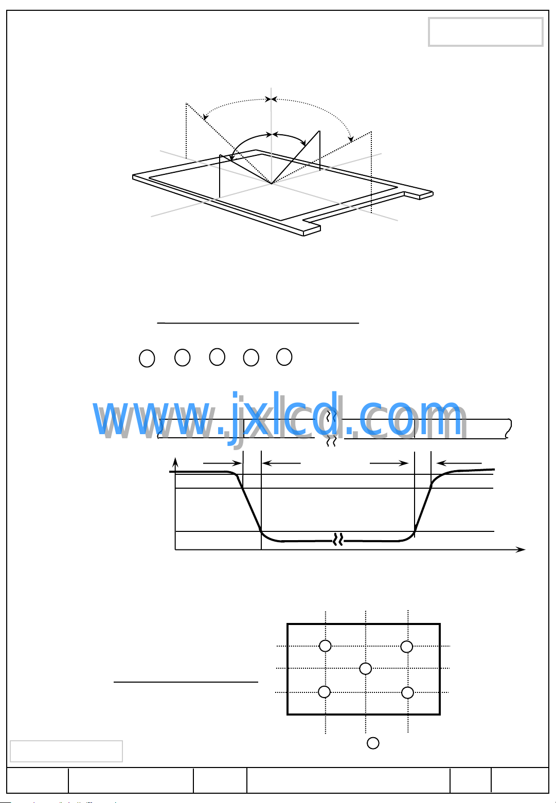
Note 1) Definition of Viewing Angle : Viewing angle range(10 C/R)
Normal Line
o
= 0
L
L
L
=90
o
x
H
,
= 0
o
R
Approval
12 O’clock
direction
y
H
= 90
o
6 O’clock
direction
o
= 90
L
Note 2) Definition of Contrast Ratio (CR) : Ratio of gray max (Gmax) ,gray min (Gmin)
at 5 points(4, 5, 7, 9, 10)
CR(4) + CR(5) + CR(7) + CR(9) + CR(10)
CR =
Points : , , , , at the figure of Note (6).
Note 3) Definition of Response time :
Display data
www.jxlcd.com
www.jxlcd.com
Optical
Response
4 9
100%
90%
10%
0%
5
White(TFT OFF) White(TFT OFF)
7
5
10
Black(TFT ON)
TR
x'y'
=90
R
TF
o
Note 4) Definition of Average Luminance of White : measure the luminance of white at 5 points.
256 512 768
Average Luminance of White ( YL,AVE )
YL4 + YL5 + YL7 + YL9 + YL10
YL,AVE =
5
Samsung Secret
Doc.No. Rev.No
04-A00-G-101122
10
9
7
5
4
: test point
Time
VIEW AREA
150
300
450
(lines)
Page
/ 33LTN156AT15-Cxx
8
Approval
Note 5) After stabilizing and leaving the panel alone at a given temperature for 30 min , the measurement
should be executed. Measurement should be executed in a stable, windless,and dark room.
30 min after lighting the backlight. This should be measured in the center of screen.
IF current : 27mA
Environment condition : Ta = 25 2 C
Photo-detector
( TOPCON SR-3 )
Field = 2
50 cm
TFT-LCD module
Center of the screen
[ Optical characteristics measurement setup ]
www.jxlcd.com
www.jxlcd.com
Note 6) Definition of 13 points white variation ( L ), CR variation( CVER ) [ ~ ]
Maximum luminance of 13 points
L =
10mm
Minimum luminance of 13 points
10mm
13 12
256 512 768
10
9
LCD panel
1 13
10mm
11
150
8
5
3
10mm
Samsung Secret
Doc.No. Rev.No
7
4
2
04-A00-G-101122
6
300
450
(lines)
1
: test point
Page
/ 33LTN156AT15-Cxx
9
3. ELECTRICAL CHARACTERISTICS
3.1 TFT LCD MODULE
Item Symbol Min. Typ. Max. Unit Note
Voltage of Power Supply VDD 3.0 3.3 3.6 V
Approval
Ta= 25 2C
Differential Input
Voltage for LVDS
Receiver Threshold
Vsync Frequency fv - 60 - Hz
Main Frequency fDCLK - 72.33 - MHz -
Rush Current IRUSH - - 1.5 A (4)
Current of Power
Supply
Note (1) Display data pins and timing signal pins should be connected.( GND = 0V )
(2) fV = 60Hz, fDCLK = 72.33MHZ, VDD = 3.3V , DC Current.
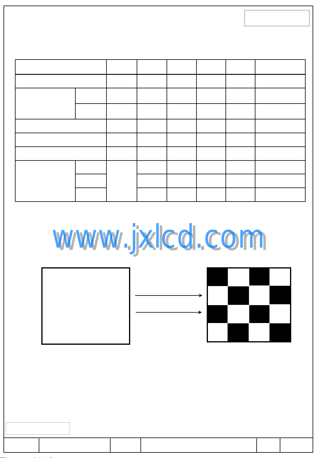
(3) Power dissipation pattern
www.jxlcd.com
www.jxlcd.com
*a) White Pattern *b) Mosaic Pattern
High VIH - - +100 mV VCM = +1.2V
Low VIL -100 - - mV
White
Mosaic - 220 - mA (2),(3)*b
V. stripe - 350 - mA (2),(3)*c
IDD
- 200 - mA (2),(3)*a
VIEW AREA
Samsung Secret
Doc.No. Rev.No
Display Brightest Gray Level
Display Darkest Gray Level
04-A00-G-101122
Page
10
/ 33LTN156AT15-Cxx
 Loading...