

Preliminary
TO
DATE :: Jun. 19. 2009.
SAMSUNG TFT-LCD
SAMSUNG TFT-LCD
MODEL NO. : LTN154AT12-401
MODEL NO. : LTN154AT12-401
NOTE :
www.jxlcd.com
-
Extension code [ -4 ] ; LTN154AT12-401
www.jxlcd.com
- Surface type [ Anti-Glare ]
Any Modification of Specification is not allowed without SEC's Permission.
SAMSUNG ELECTRONICS CO., LTD.
Samsung Secret
Doc.No. Rev.No
04-P04-S-090619
Page
/ 28LTN154AT12-401
1
CONTENTS
Preliminary
Revision History
General Description
1. Absolute Maximum Ratings
1.1 Absolute Ratings of environment
1.2 Electrical Absolute Ratings
2. Optical Characteristics
3. Electrical Characteristics
3.1 TFT LCD Module
3.2 Backlight Unit
4. Block Diagram
4.1 TFT LCD Module
5. Input Terminal Pin Assignment
5.1 Input Signal & Power
5.2 LVDS Interface
5.3 Timing Diagrams of LVDS For Transmitting
5.4 Input Signals, Basic Display Colors and Gray Scale of Each Color.
5.5 Pixel format
www.jxlcd.com
www.jxlcd.com
5.6 LED FPC Connector & Pin Assignment
- - - - - - - - - - - - - - - - - - - ( 3 )
- - - - - - - - - - - - - - - - - - - ( 4 )
- - - - - - - - - - - - - - - - - - - ( 5 )
- - - - - - - - - - - - - - - - - - - ( 7 )
- - - - - - - - - - - - - - - - - - - ( 10 )
- - - - - - - - - - - - - - - - - - - ( 13 )
- - - - - - - - - - - - - - - - - - - ( 14 )
6. Interface Timing
6.1 Timing Parameters
6.2 Timing Diagrams of interface Signal
6.3 Power ON/OFF Sequence
7. Outline Dimension
8. Packing
9. Markings & Others
10. General Precaution
11. EDID
Samsung Secret
- - - - - - - - - - - - - - - - - - - ( 21 )
- - - - - - - - - - - - - - - - - - - ( 23 )
-- - - - - - - - - - - - - - - - - - ( 25 )
-- - - - - - - - - - - - - - - - - - ( 26 )
-- - - - - - - - - - - - - - - - - - ( 28 )
- - - - - - - - - - - - - - - - - - - ( 30 )
Doc.No. Rev.No
04-P04-S-090619
Page
/ 28LTN154AT12-401
2
REVISION HISTORY
REVISION HISTORY
Date Revision No. Page Summary
Oct. 31. 2008 P00 All LTN154AT12-X Model spec was issued first
Nov.17.2008 P01 All LTN154AT12-401 Model name fixed.
FPC Connector pin map was updated .20P02Dec.26.2008
Preliminary
P03Jan. 7. 2009
P04Jan.9.2009
www.jxlcd.com
www.jxlcd.com
12
24
26
29
12
24
LED forward current was updated.
Outline drawing was updated.
Product Markings and Others( Error-typo correction )
EDID was updated
Back-light Unit was updated
Outline drawing was updated.
Samsung Secret
Doc.No. Rev.No
04-P04-S-090619
Page
/ 28LTN154AT12-401
3
Preliminary
GENERAL DESCRIPTION
DESCRIPTION
LTN154AT12 is a color active matrix TFT (Thin Film Transistor) liquid crystal display
(LCD) that uses amorphous silicon TFT as a switching devices. This model is composed of
a TFT LCD panel, a driver circuit and a backlight unit. The resolution of a 15.4" contains
1,280 x 800 pixels and can display up to 262,144 colors. 6 O'clock direction is the Optimum
viewing angle.
FEATURES
• High contrast ratio, high aperture structure
• 1280 x 800 pixels resolution
• Low power consumption
• Fast Response
• DE(Data enable) only mode
• 3.3V LVDS Interface
• Onboard EEDID chip
• LED BLU
• Color gamut 45%
APPLICATIONS
• Notebook PC
• If the usage of this product is not for PC application, but for others, please contact SEC.
www.jxlcd.com
GENERAL INFORMATION
Display area
Driver element
Display colors
Number of pixel
Pixel arrangement
Pixel pitch
www.jxlcd.com
Item Specification Unit Note
331.2(H) x 207.0(V) (15.4” diagonal ) mm
a-Si TFT active matrix
262,144
1280 x RGB(3) x 800 pixel 16 : 10
RGB vertical stripe
0.2588(H) x 0.2588(V) (TYP.) mm
Display Mode
Surface treatment HAZE 25, HARD-COATING 3H, AG
Samsung Secret
Doc.No. Rev.No
Normally white
04-P04-S-090619
Page
/ 28LTN154AT12-401
4
Mechanical Information
Item Min. Typ. Max. Unit Note
Horizontal (H) 343.5 344.0 344.5 mm
Module
size
Note (1) Measurement condition of outline dimension
Vertical (V) 221.5 222.0 222.6 mm
Depth (D) - - 6.5 mm (1)
Weight - 560 (575) g
. Equipment : Vernier Calipers
. Push Force : 500g ⋅f (minimum)
1. ABSOLUTE MAXIMUM RATINGS
1.1 ENVIRONMENTAL ABSOLUTE RATINGS
Item Symbol Min. Max. Unit Note
Preliminary
Storage temperate T
Operating temperate
(Temperature of glass surface)
Shock ( non-operating ) Snop -
Vibration (non-operating) Vnop - 2.41 G (4),(5)
Note (1) Temperature and relative humidity range are shown in the figure below.
www.jxlcd.com
www.jxlcd.com
95 % RH Max. ( 40 OC ≥ Ta)
Maximum wet - bulb temperature at 39 OC or less. (Ta > 40 OC) No condensation.
(2) 3ms, half sine wave, one time for ±X,±Y,±Z.
(3) 18ms, Trapezoidal wave, one time for ±X,±Y,±Z.
(4) 5~500 Hz, Random vibration, 30 min for X,Y,Z.
(5) At testing Vibration and Shock, the fixture in holding the Module to be tested have to be
hard and rigid enough so that the Module would not be twisted or bent by the fixture.
100
95
80
60
STG
T
OPR
Relative Humidity ( %RH)
Operating Range
-20 60 °C (1)
0 50 °C (1)
210
G
50 (3),(5)
(2),(5)
40
20
8
Storage Range
5
0
-40 -20 0 20 40 60 80
Temperature (OC)
Samsung Secret
Doc.No. Rev.No
04-P04-S-090619
Page
/ 28LTN154AT12-401
5
1.2 ELECTRICAL ABSOLUTE RATINGS
(1) TFT LCD MODULE
Preliminary
Item Symbol Min. Max. Unit Note
Power Supply Voltage V
Logic Input Voltage V
Note (1) Within Ta (25 ± 2 °C )
DD
DD
V
DD
– 0.3 V
V
DD
– 0.3 V
VDD=3.3V, V
DD
+ 0.3 V (1)
DD
+ 0.3 V (1)
SS
= GND = 0V
www.jxlcd.com
www.jxlcd.com
Samsung Secret
Doc.No. Rev.No
04-P04-S-090619
Page
/ 28LTN154AT12-401
6
Preliminary
2. OPTICAL CHARACTERISTICS
The following items are measured under stable conditions. The optical characteristics
should be measured in a dark room or equivalent state with the methods shown in Note (5).
Measuring equipment : TOPCON BM-5A and PR-650
Item Symbol Condition Min. Typ. Max Unit Note
Contrast Ratio
(5 Points)
Response Time at Ta
( Rising + Falling )
Average Luminance
of White (5 Points)
Red
Color
Chromaticity
( CIE )
Green
Blue
www.jxlcd.com
www.jxlcd.com
* Ta = 25 ± 2 °C, VDD=3.3V, fv= 60Hz, f
CR - 300 - -
T
RT_B/W
YL,
R
R
G
G
B
B
AVE
X
Y
X
Y
X
Y
Normal
Viewing
Angle
φ = 0
θ = 0
- 16 25 msec (1), (3)
190 220 - cd/m
(0.535) (0.585) (0.635)
(0.291) (0.341) (0.391)
(0.292) (0.342) (0.392)
(0.512) (0.562) (0.612)
(0.101) (0.151) (0.201)
(0.063) (0.113) (0.163)
DCLK
= 72.2 MHz
AG
(1), (2), (5)
2
-
(1), (4)
(1), (5)
PR-650
Viewing
Angle
13 Points
White Variation
5 Points
White Variation
Samsung Secret
White
Hor.
Ver.
W
W
X
Y
θ
L
θ
H
CR ≥ 10
φ
H
φ
L
δ
L
δ
L
0.283 0.313 0.343
0.299 0.329 0.359
- 45 -
- 45 -
- 15 -
- 35 -
60% - (1.7) - (6)
80% - - % (6)
Degrees (1), (5)
BM-5A
%45%Color gamut
Doc.No. Rev.No
04-P04-S-090619
Page
/ 28LTN154AT12-401
7
Note 1) Definition of Viewing Angle : Viewing angle range( 10
Normal Line
o
φ = 0
,
θ = 0
θ
L
φ
H
θL =90
φ
o
x
L
≤≤≤≤
C/R, 100
o
θ
R
≤≤≤≤
C/R )
y
Preliminary
12 O’clock
direction
φH= 90
o
6 O’clock
direction
φL= 90
Note 2) Definition of Contrast Ratio (CR) : Ratio of gray max (Gmax) ,gray min (Gmin)
at 5 points(4, 5, 7, 9, 10)
Note 3) Definition of Response time :
Display data
Optical
Response
o
CR(4) + CR(5) + CR(7) + CR(9) + CR(10)
CR =
Points : , , , , at the figure of Note (6).
www.jxlcd.com
www.jxlcd.com
4 9
100%
90%
10%
0%
5
Gray 32(TFT OFF) Gray 32(TFT OFF)
White(TFT OFF) White(TFT OFF)
7
5
10
Gray 48 (TFT ON)
Black(TFT ON)
T
R
x'y'
θR=90
T
F
o
Note 4) Definition of Average Luminance of White : measure the luminance of white at 5 points.
(320) ( 640) (960)
Average Luminance of White ( Y
YL4+ YL5+ YL7+ YL9+ Y
Y
L,AVE
=
Samsung Secret
Doc.No. Rev.No
5
L,AVE
)
L10
10
9
7
5
4
: test point
04-P04-S-090619
Time
VIEW AREA
(200)
(400)
(600)
(lines)
Page
/ 28LTN154AT12-401
8
Preliminary
Note 5) After stabilizing and leaving the panel alone at a given temperature for 30 min , the measurement
should be executed. Measurement should be executed in a stable, windless,and dark room.
30 min after lighting the backlight. This should be measured in the center of screen.
Environment condition : Ta = 25 ± 2 °C
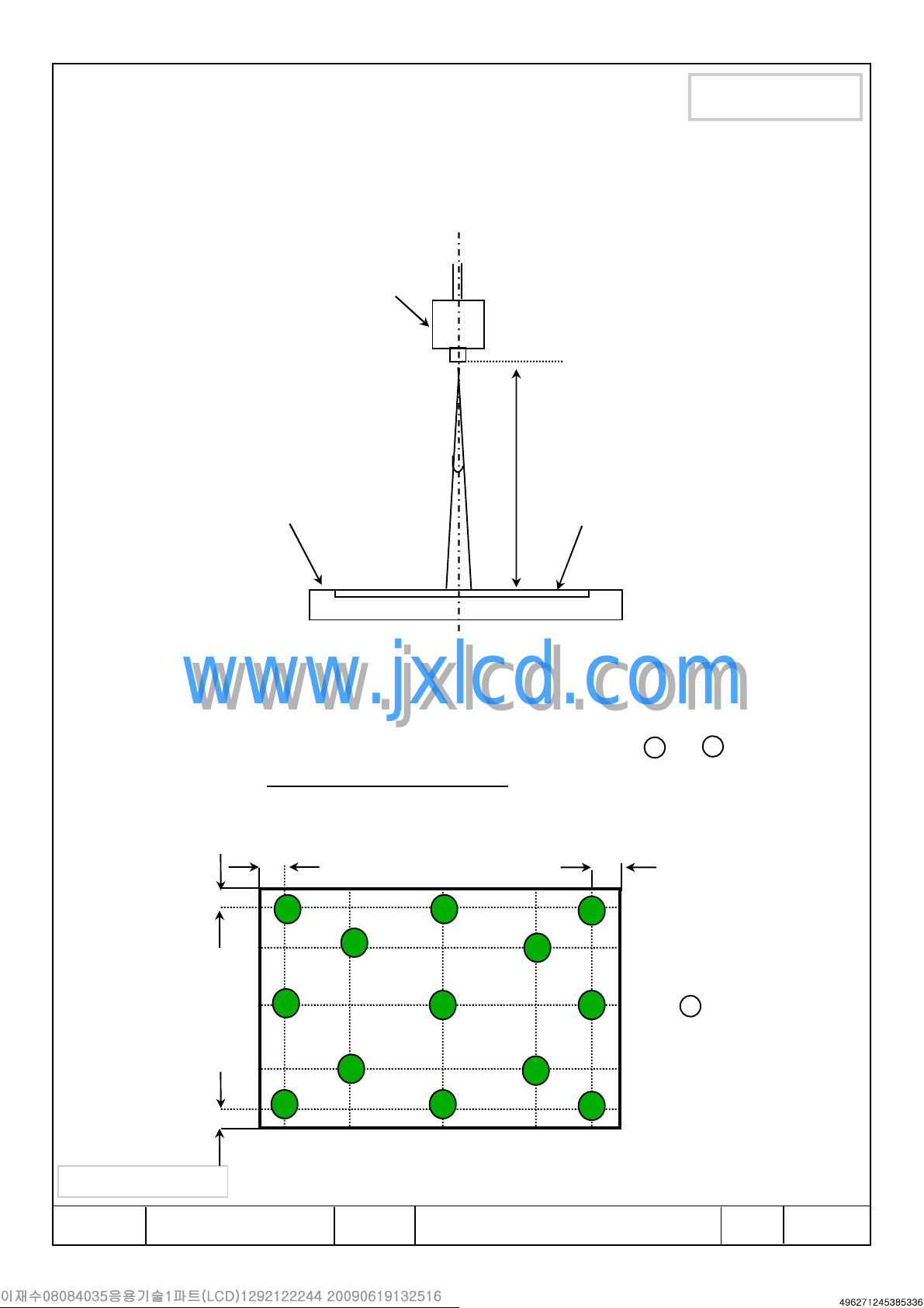
Photo-detector
( TOPCON BM-5A
PR-650 )
Field
= 2°
50 cm
TFT-LCD module
Center of the screen
[ Optical characteristics measurement setup ]
www.jxlcd.com
www.jxlcd.com
Note 6) Definition of 13 points white variation (
Maximum luminance of 13 points
δL=
Minimum luminance of 13 points
10mm
10mm
13 12
320 640
10
δ
L
), CR variation( C
960
LCD panel
VER
) [ ~ ]
1 13
10mm
11
9
200
8
5
3
10mm
Samsung Secret
Doc.No. Rev.No
7
4
2
04-P04-S-090619
6
400
600
(lines)
1
: test point
Page
/ 28LTN154AT12-401
9
3. ELECTRICAL CHARACTERISTICS
3.1 TFT LCD MODULE
Item Symbol Min. Typ. Max. Unit Note
Preliminary
Ta= 25 ± 2°C
Voltage of Power Supply V
Differential Input
Voltage for LVDS
Receiver Threshold
Vsync Frequency fv - (60) - Hz
Hsync Frequency f
Main Frequency f
Rush Current I
Current of Power
Supply
Note (1) Display data pins and timing signal pins should be connected.( GND = 0V )
(2) fV= 60Hz, f
(3) Power dissipation pattern
www.jxlcd.com
www.jxlcd.com
High V
Low V
White
Mosaic - (350) - mA (2),(3)*b
V. stripe - (450) (520) mA (2),(3)*c
DCLK
= 72.2MHz, VDD= 3.3V , DC Current.
DD
IH
IL
H
DCLK
RUSH
I
DD
3.0 3.3 3.6 V
- - +100 mV V
-100 - - mV
- (50.04) - KHz
- (72.2) (85) MHz
- - (1.5) A (4)
- (300) - mA (2),(3)*a
CM
= +1.2V
*a) White Pattern *b) Mosaic Pattern
VIEW AREA
Samsung Secret
Display Brightest Gray Level
Display Darkest Gray Level
Doc.No. Rev.No
04-P04-S-090619
Page
10
/ 28LTN154AT12-401
 Loading...