

Approval
TO
DATE
SAMSUNG TFT-LCD
SAMSUNG TFT-LCD
MODEL NO. : LTN154AT09
MODEL NO. : LTN154AT09
NOTE :
www.jxlcd.com
: Computer Div.
: June. 20, 2008.
-
Extension code [ -8 ] ; LTN154AT09-8
www.jxlcd.com
- Surface type [ Anti Glare ]
Any Modification of Specification is not allowed without SEC's Permission.
APPROVED BY :
PREPARED BY : LCD Development Group 1 (Mobile)
SAMSUNG ELECTRONICS CO., LTD.
Samsung Secret
Doc.No. Rev.No
04-A00-G-080620
Page
/ 31LTN154AT09-8
1
CONTENTS
Approval
Revision History
General Description
1. Absolute Maximum Ratings
1.1 Absolute Ratings of environment
1.2 Electrical Absolute Ratings
2. Optical Characteristics
3. Electrical Characteristics
3.1 TFT LCD Module
3.2 Backlight Unit
4. Block Diagram
4.1 TFT LCD Module
4.2 Backlight Unit
5. Input Terminal Pin Assignment
5.1 Input Signal & Power
5.2 LVDS Interface
5.3 Backlight Unit
5.4 Timing Diagrams of LVDS For Transmitting
5.5 Input Signals, Basic Display Colors and Gray Scale of Each Color.
www.jxlcd.com
www.jxlcd.com
5.6 Pixel format
5.7 Inverter Signals & Power
- - - - - - - - - - - - - - - - - - - ( 3 )
- - - - - - - - - - - - - - - - - - - ( 4 )
- - - - - - - - - - - - - - - - - - - ( 5 )
- - - - - - - - - - - - - - - - - - - ( 7 )
- - - - - - - - - - - - - - - - - - - ( 10 )
- - - - - - - - - - - - - - - - - - - ( 13 )
- - - - - - - - - - - - - - - - - - - ( 15 )
6. Interface Timing
6.1 Timing Parameters
6.2 Timing Diagrams of interface Signal
6.3 Power ON/OFF Sequence
7. Outline Dimension
8. Packing
9. Markings & Others
10. General Precaution
Samsung Secret
- - - - - - - - - - - - - - - - - - - ( 21 )
- - - - - - - - - - - - - - - - - - - ( 23 )
-- - - - - - - - - - - - - - - - - - ( 24 )
-- - - - - - - - - - - - - - - - - - ( 25 )
- - - - - - - - - - - - - - - - - - - ( 27 )
Doc.No. Rev.No
04-A00-G-080620
Page
/ 31LTN154AT09-8
2
REVISION HISTORY
REVISION HISTORY
. The approval specification was issued.AllA00Jun. 20. 2008
Approval
SummaryPageRevision No.Date
www.jxlcd.com
www.jxlcd.com
Samsung Secret
Doc.No. Rev.No
04-A00-G-080620
Page
/ 31LTN154AT09-8
3
Approval
GENERAL DESCRIPTION
DESCRIPTION
LTN154AT09-8 is a color active matrix TFT (Thin Film Transistor) liquid crystal display
(LCD) that uses amorphous silicon TFT as a switching devices. This model is composed of
a TFT LCD panel, a driver circuit and a backlight unit. The resolution of a 15.4" contains
1,280 x 800 pixels and can display up to 262,144 colors. 6 O'clock direction is the Optimum
viewing angle.
FEATURES
• High contrast ratio, high aperture structure
• 1280 x 800 pixels resolution
• Low power consumption
• Fast Response
• Single CCFL
• DE(Data enable) only mode
• 3.3V LVDS Interface
• Onboard EEDID chip
APPLICATIONS
• Notebook PC
• If the usage of this product is not for PC application, but for others, please contact SEC.
www.jxlcd.com
GENERAL INFORMATION
Display area
Driver element
Display colors
Number of pixel
Pixel arrangement
Pixel pitch
www.jxlcd.com
mm331.2(H) x 207.0(V) (15.4” diagonal )
a-Si TFT active matrix
262,144
RGB vertical stripe
mm0.2588(H) x 0.2588(V) (TYP.)
NoteUnitSpecificationItem
16 : 10pixel1280 x RGB(3) x 800
Display Mode
Surface treatment
Samsung Secret
Doc.No. Rev.No
Normally white
04-A00-G-080620
Page
GlareHaze 25, Hard-Coating 3H
/ 31LTN154AT09-8
4
Mechanical Information
Approval
Max.
344.5
Module
size
222.5
6.5
570
1. ABSOLUTE MAXIMUM RATINGS
1.1 ENVIRONMENTAL ABSOLUTE RATINGS
Operating temperate
(Temperature of glass surface)
Note (1) Temperature and relative humidity range are shown in the figure below.
95 % RH Max. (40 °C ≥ Ta)
Maximum wet - bulb temperature at 39
www.jxlcd.com
www.jxlcd.com
100
Relative Humidity ( %RH)
90
O
C or less. (Ta > 40 °C ) No condensation
( 40,90 )
NoteUnitTyp.Min.Item
mm344.0343.5Horizontal (H)
w/o inverter ass’y
mm222.0221.5Vertical (V)
mm--Depth (D)
LCD module onlyg555-Weight
NoteUnitMax.Min.SymbolItem
(1),(5)°C60-20 TSTGStorage temperate
(1),(5)°C500TOPR
(2),(4)G240-SnopShock ( non-operating )
(3),(4)G2.41-VnopVibration (non-operating)
80
60
40
20
-40 -20 0 20 40 60 80
Operating Range
Storage Range
5
0
Temperature (
(2) 2ms, half sine wave, one time for ±X, ±Y, ± Z.
(3) 5 - 500 Hz, random vibration, 30min for X, Y, Z.
(4) At testing Vibration and Shock, the fixture in holding the Module to be tested have to be
hard and rigid enough so that the Module would not be twisted or bent by the fixture.
(5) If product is used for extended time excessively or exposed to high temperatures for extended time,
there is a possibility of wide viewing angle film damage which could affect visual characteristics
Samsung Secret
Doc.No. Rev.No
( 50,50.4 )
( 60,27.7 )
O
C)
04-A00-G-080620
Page
.
/ 31LTN154AT09-8
5
1.2 ELECTRICAL ABSOLUTE RATINGS
(1) TFT LCD MODULE
DD
V
=3.3V, V
Approval
SS
= GND = 0V
NoteUnitMax.Min.SymbolItem
DD
DD
+ 0.3V
+ 0.3V
Power Supply Voltage
Logic Input Voltage
Note (1) Within Ta (25 ± 2 °C )
DD
DD
DD
DD
– 0.3V
– 0.3V
(2) BACK-LIGHT UNIT
Lamp Current
Lamp frequency
Note 1) Permanent damage to the device may occur if maximum values are exceeded
Functional operation should be restricted to the conditions described under normal operating conditions.
www.jxlcd.com
www.jxlcd.com
L
L
(1)VV
(1)VV
Ta = 25 ± 2 °C
NoteUnitMax.Min.SymbolItem
(1)mArms7.03.0I
(1)kHz8040F
Samsung Secret
Doc.No. Rev.No
04-A00-G-080620
Page
/ 31LTN154AT09-8
6
Approval
2. OPTICAL CHARACTERISTICS
The following items are measured under stable conditions. The optical characteristics
should be measured in a dark room or equivalent state with the methods shown in Note (5).
Measuring equipment : TOPCON BM-5A and PR-650
Contrast Ratio
(5 Points)
Response Time at Ta
( Rising + Falling )
Average Luminance
of White (5 Points)
Red
Green
Color
Chromaticity
( CIE )
www.jxlcd.com
www.jxlcd.com
Blue
* Ta = 25 ± 2 °C, VDD=3.3V, fv= 60Hz, f
CR
RT_B/W
L,AVE
X
R
Y
R
Normal
G
X
Y
G
B
X
Y
B
Viewing
Angle
φ = 0
θ = 0
DCLK
= 71.26MHz, IL= 6.0 mArms
Unit
-
msec
2
-220200Y
0.6100.5900.570
0.3600.3400.320
0.3500.3300.310
0.5650.5450.525
0.1750.1550.135
0.1550.1350.115
cd/m
-
NoteMaxTyp.Min.ConditionSymbolItem
(1), (2), (5)-500300
(1), (3)2516-T
L
=6.0mA
I
(1), (4)
(1), (5)
PR-650
X
White
Y
L
θ
Hor.
Viewing
Angle
Ver.
13 Points
White Variation
Samsung Secret
H
CR ≥ 10
H
L
L
Doc.No. Rev.No
0.3330.3130.293W
0.3490.3290.309W
04-A00-G-080620
--40
--40θ
--15φ
--30φ
Degrees
-
Page
(1), (5)
BM-5A
(6)1.7--δ
7
/ 31LTN154AT09-8
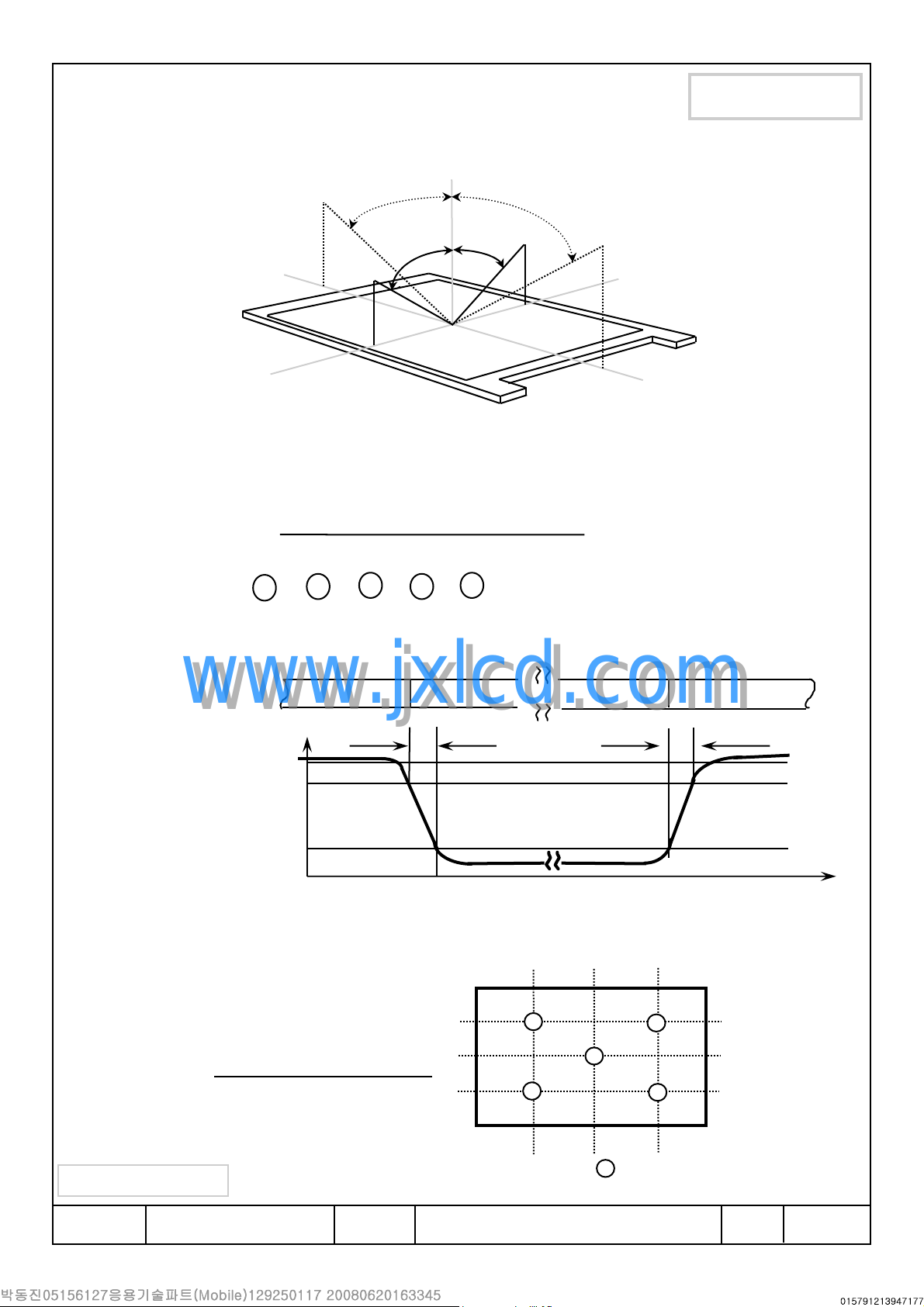
Note 1) Definition of Viewing Angle : Viewing angle range( 10
Normal Line
o
φ = 0
,
θ = 0
θ
L
φ
H
θL =90
φ
o
x
L
≤≤≤≤
C/R, 100
o
θ
R
≤≤≤≤
C/R )
y
Approval
12 O’clock
direction
φH= 90
o
6 O’clock
direction
φL= 90
Note 2) Definition of Contrast Ratio (CR) : Ratio of gray max (Gmax) ,gray min (Gmin)
at 5 points(4, 5, 7, 9, 10)
Points : , , , , at the figure of Note (6).
Note 3) Definition of Response time :
Display data
Optical
Response
o
CR(4) + CR(5) + CR(7) + CR(9) + CR(10)
CR =
4
www.jxlcd.com
www.jxlcd.com
100%
90%
10%
0%
5
Gray 32(TFT OFF) Gray 32(TFT OFF)
White(TFT OFF)
7
5
10
9
Gray 48 (TFT ON)
Black(TFT ON)
T
R
x'y'
=90
θ
R
White(TFT OFF)
T
F
o
Note 4) Definition of Average Luminance of White : measure the luminance of white at 5 points.
(320) ( 640) (960)
Average Luminance of White ( Y
Y
L4 + YL5 + YL7 + YL9 + YL10
Y
L,AVE
=
Samsung Secret
Doc.No. Rev.No
5
L,AVE
)
10
9
7
5
4
: test point
04-A00-G-080620
Time
VIEW AREA
(200)
(400)
(600)
(lines)
Page
/ 31LTN154AT09-8
8
Approval
Note 5) After stabilizing and leaving the panel alone at a given temperature for 30 min , the measurement
should be executed. Measurement should be executed in a stable, windless,and dark room.
30 min after lighting the backlight. This should be measured in the center of screen.
Lamp current : 6.0mA
Environment condition : Ta = 25 ± 2 °C
Photo-detector
( TOPCON BM-5A
PR-650 )
= 2°
Field
50 cm
TFT-LCD module
Center of the screen
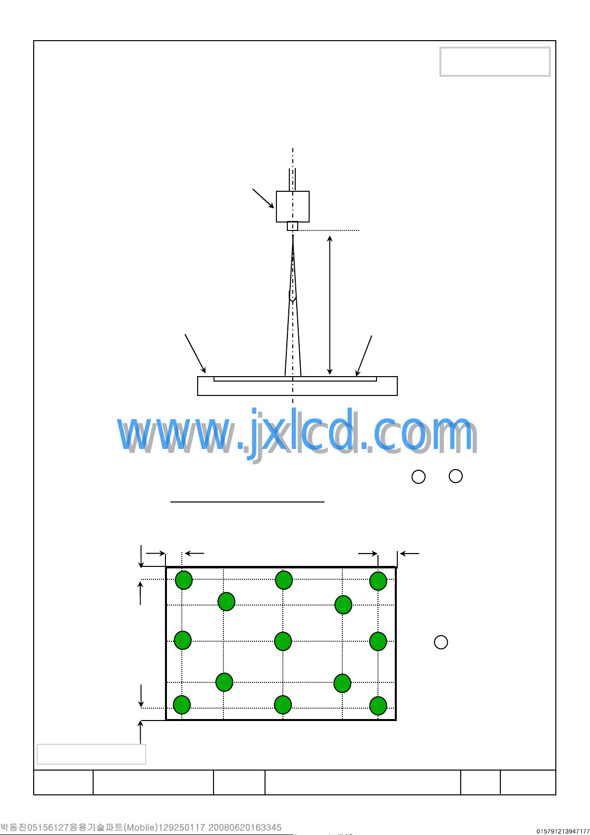
[ Optical characteristics measurement setup ]
www.jxlcd.com
www.jxlcd.com
Note 6) Definition of 13 points white variation (
Maximum luminance of 13 points
δL=
Minimum luminance of 13 points
10mm
10mm
13
320 640
10
LCD panel
δ
L
), CR variation( CVER ) [ ~ ]
10mm
960
12
9
11
1 13
200
8
5
3
10mm
Samsung Secret
Doc.No. Rev.No
7
4
2
04-A00-G-080620
6
400
600
(lines)
1
: test point
Page
/ 31LTN154AT09-8
9
3. ELECTRICAL CHARACTERISTICS
3.1 TFT LCD MODULE
Approval
Ta= 25 ± 2°C
NoteUnitMax.Typ.Min.SymbolItem
Voltage of Power Supply
Differential Input
Voltage for LVDS
Receiver Threshold
Hsync Frequency
Main Frequency
Rush Current
Current of Power
Supply
Note (1) Display data pins and timing signal pins should be connected.( GND = 0V )
(2) f
V
= 60Hz, f
(3) Power dissipation pattern
www.jxlcd.com
www.jxlcd.com
High
Low
White
DCLK
= 71.26MHz, VDD= 3.3V , DC Current.
DD
IH
IL
H
DCLK
RUSH
I
DD
V3.63.33.0V
CM
= +1.2VmV+100--V
V
mV---100V
Hz-60-fvVsync Frequency
KHz-48.96-f
MHz-71.26-f
(4)A1.5--I
(2),(3)*amA-300(2),(3)*bmA-310-Mosaic
(2),(3)*cmA500380-V. stripe
*a) White Pattern *b) Mosaic Pattern
VIEW AREA
Samsung Secret
Display Brightest Gray Level
Display Darkest Gray Level
Doc.No. Rev.No
04-A00-G-080620
Page
10
/ 31LTN154AT09-8
 Loading...