

Approval
TO
DATE
SAMSUNG TFT-LCD
SAMSUNG TFT-LCD
MODEL NO.:LTN150PF-L04
MODEL NO.:LTN150PF-L04
NOTE : Extension code [ -0 ] → LTN150PF-L04-0
www.jxlcd.com
:
: May. 2009
Surface type [ Anti-Glare ]
www.jxlcd.com
Any Modification of Specification is not allowed without SEC's Permission.
APPROVED BY :
PREPARED BY : LCD Application Engineering Group 1, TCS Team
SAMSUNG ELECTRONICS CO., LTD.
SEC Secret
Doc.No. Rev.No Page / 30LTN150PF-L04 1
05-A00-S-080417

CONTENTS
Approval
Revision History
General Description
1. Absolute Maximum Ratings
1.1 Absolute Ratings of environment
1.2 Electrical Absolute Ratings
2. Optical Characteristics
3. Electrical Characteristics
3.1 TFT LCD Module
3.2 Backlight Unit
4. Block Diagram
4.1 TFT LCD Module
4.2 Backlight Unit
5. Input Terminal Pin Assignment
5.1 Input Signal & Power
5.2 LVDS Interface
5.3 Backlight Unit
5.4 Timing Diagrams of LVDS For Transmitting
www.jxlcd.com
www.jxlcd.com
5.5 Input Signals, Basic Display Colors and Gray Scale of Each Color.
5.6 Pixel format
- - - - - - - - - - - - - - - - - - - ( 3 )
- - - - - - - - - - - - - - - - - - - ( 4 )
- - - - - - - - - - - - - - - - - - - ( 5 )
-- - - - - - - - - - - - - - - - - - - ( 7 )
- - - - - - - - - - - - - - - - - - - ( 10 )
- - - - - - - - - - - - - - - - - - - ( 13 )
- - - - - - - - - - - - - - - - - - - ( 14 )
6. Interface Timing
6.1 Timing Parameters(DE Mode)
6.2 Timing Diagrams of interface Signal (DE Mode)
6.3 Power ON/OFF Sequence
7. Mechanical Outline Dimension
8. Packing
9. Marking & Others
10. General Precautions
11. EEDID
SEC Secret
Doc.No. Rev.No Page / 30LTN150PF-L04 2
05-A00-S-080417
- - - - - - - - - - - - - - - - - - - ( 20 )
- - - - - - - - - - - - - - - - - - - ( 22 )
-- - - - - - - - - - - - - - - - - - ( 23 )
- - - - - - - - - - - - - - - - - - - ( 24 )
-- - - - - - - - - - - - - - - - - - ( 26 )
- - - - - - - - - - - - - - - - - - - ( 28 )
REVISION HISTORY
REVISION HISTORY
Approval
Date
Revision
No.
SummaryPage
. The approval spec was issuedALLA00Apr. 17. 2008
www.jxlcd.com
www.jxlcd.com
SEC Secret
Doc.No. Rev.No Page / 30LTN150PF-L04 3
05-A00-S-080417
Approval
GENERAL DESCRIPTION
DESCRIPTION
LTN150PF-L04 is a color active matrix TFT (Thin Film Transistor) liquid crystal display
(LCD) that uses amorphous silicon TFT as a switching devices. This model is composed of
a TFT LCD panel, a driver circuit and a backlight system. The resolution of a 15.0” contains
1400 x 1050 pixels and can display up to 262,144 colors. 6 O'clock direction is the Optimum
viewing angle.
FEATURES
• Thin and light weight
• High contrast ratio
• SXGA-Plus (1400x1050 pixels) resolution
• Low power consumption
• DE (Data enable) only mode.
• LVDS Interface with 2 pixel / clock (2 channel)
• On board EDID chip, SPWG-B style
• Green product (complied with RoHS requirement)
APPLICATIONS
• Notebook PC
• If the usage of this product is not for PC application, but for others, please contact SEC
www.jxlcd.com
GENERAL INFORMATION
Display area 304.1(H)X228.1(V) (15.0”diagonal)
Driver element a-si TFT active matrix
Display colors 262,144
Number of pixel 1400 x 1050 (SXGA-Plus)
Pixel arrangement RGB vertical stripe
Pixel pitch 0.2175(H) x 0.2175(V)
www.jxlcd.com
ITEM SPECIFICATION
UNIT
mm
pixel
mm
NOTE
Normally whiteDisplay Mode
Surface treatment
SEC Secret
Doc.No. Rev.No Page / 30LTN150PF-L04 4
HAZE 25, HARD-COATING 3H
05-A00-S-080417
Mechanical Information
Approval
ITEM TYP. MAX. NOTE
Horizontal (H)
Module
Size
Note (1) Depth of signal interface connector part.
Vertical (V)
Depth (D) -
Weight
MIN.
316.8
241.6
1. ABSOLUTE MAXIMUM RATINGS
1.1 ENVIRONMENTAL ABSOLUTE RATINGS
ITEM UNIT
Storage temperate
Operating temperate
(Temperature of glass surface)
SYMBOL MIN. MAX.
T
STG
T
OPR
317.3
242.1 242.6
5.7 6.0
550g
-20 60
0
50
317.8
560g
O
O
w/o Inverter
NOTE
C
C
(1)
(1)
Shock ( non-operating )
Vibration (non-operating)
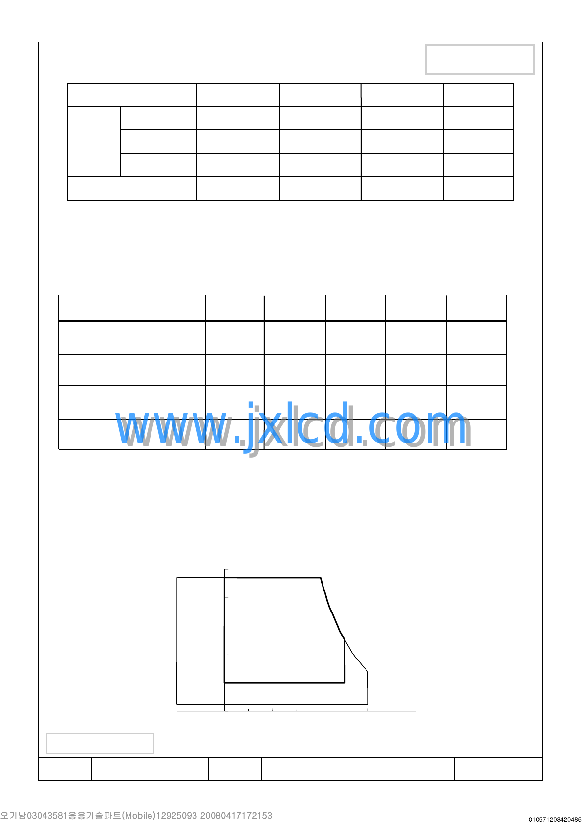
Note (1) Temperature and relative humidity range are shown in the figure below.
SEC Secret
www.jxlcd.com
www.jxlcd.com
95 % RH Max. ( 40°C ≥ Ta)
Maximum wet - bulb temperature at 39°C or less. (Ta > 40°C) No condensation.
(2) 2ms, half sine wave, one time for ±X, ±Y, ± Z.
(3) 5 - 500 Hz, random vibration, 30min for X, Y, Z.
(4) At testing Vibration and Shock, the fixture in holding the Module to be tested has to be
hard and rigid enough, so that the Module would not be twisted or bent by the fixture.
-40 -20 0 20 40 60 80
100
80
60
40
20
Snop
Vnop
Relative Humidity ( %RH)
95
Operating Range
Storage Range
5
0
Temperature (
-
-
O
C)
240 G
2.41
( 40,95 )
( 50,50.4 )
G
( 60,27.7 )
(2), (4)
(3), (4)
Doc.No. Rev.No Page / 30LTN150PF-L04 5
05-A00-S-080417
1.2 ELECTRICAL ABSOLUTE RATINGS
Approval
(1) TFT LCD MODULE
Power Supply Voltage
Logic Input Voltage
NOTE (1) Within Ta ( 25 ± 2 OC )
(2) BACK-LIGHT UNIT
Lamp Current
Lamp frequency
NOTE (1) Permanent damage to the device may occur if maximum values are exceeded.
Functional operation should be restricted to the conditions described under Normal Operating
Conditions.
L
L
DD
IN
VDD=3.3V, V
Ta = 25 ± 2 OC
SS
= GND = 0V
NoteUnitMax.Min.SymbolItem
NoteUnitMax.Min.SymbolItem
(1)VVDD+ 0.3VDD- 0.3V
(1)VVDD+ 0.3VDD- 0.3V
(1)mArms7.02.0I
(1)kHz8040F
1.3 Others
www.jxlcd.com
www.jxlcd.com
- MTBF : 50000Hr(except for back-light lamp)
SEC Secret
Doc.No. Rev.No Page / 30LTN150PF-L04 6
05-A00-S-080417
Approval
2. OPTICAL CHARACTERISTICS
The following items are measured under stable conditions. The optical characteristics
should be measured in a dark room or equivalent state with the methods shown in Note (5).
Measuring equipment : TOPCON BM-5A and PR-650
Contrast Ratio
(5 Points)
Response
Time at Ta
Average Luminance
of White (5 Points)
www.jxlcd.com
Green
www.jxlcd.com
Color
Chromaticity
( CIE )
Rising
Falling
Red
Blue
* Ta = 25 ± 2°C , VDD=3.3V, fv= 60Hz, f
R
T
T
AVE
X
Y
X
Y
X
Y
Normal
Viewing
Angle
φ = 0
θ = 0
DCLK
=54MHz, IL= 6.0 mA
Unit
--300CR
2010-T
5030-
-200175YL,
0.6060.5760.546R
0.3710.3410.311R
0.3530.3230.293G
0.5620.5320.502G
0.1830.1530.123B
0.1620.1320.102B
-
cd/m
-
2
NoteMaxTyp.Min.ConditionSymbolItem
(1), (2),
(5)
(1), (3)msec
IL=6.0mA
(1), (4)
(1), (5)
PR-650
X
White
Y
θ
L
Hor.
Viewing
Angle
Ver.
13 Points
White Variation
SEC Secret
Doc.No. Rev.No Page / 30LTN150PF-L04 7
H
CR ≥ 10
H
L
L
--δ
05-A00-S-080417
0.3430.3130.283W
0.3590.3290.299W
-60-
-60-θ
-45-φ
-45-φ
2.2
(45%)
Degrees
%
(1), (5)
BM-5A
(6)
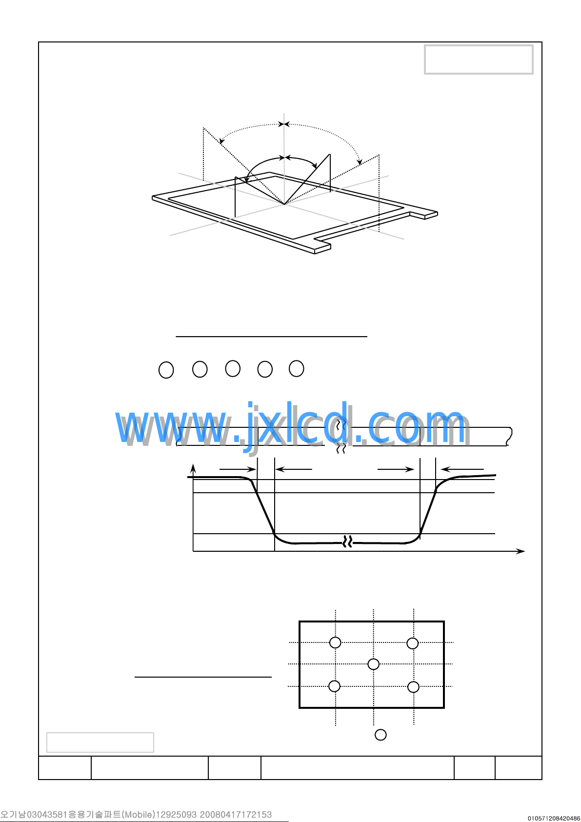
Note 1) Definition of Viewing Angle : Viewing angle range(10
Normal Line
o
φ = 0
,
θ = 0
θ
L
φ
H
θL =90
φ
o
x
L
≤≤≤≤
o
C/R)
θ
R
Approval
12 O’clock
y
direction
φH= 90
o
6 O’clock
direction
φL= 90
Note 2) Definition of Contrast Ratio (CR) : Ratio of gray max (Gmax) ,gray min (Gmin)
at 5 points(4, 5, 7, 9, 10)
Note 3) Definition of Response time :
Display data
Optical
Response
o
CR(4) + CR(5) + CR(7) + CR(9) + CR(10)
CR =
Points : , , , , at the figure of Note (6).
www.jxlcd.com
www.jxlcd.com
4 9
100%
90%
10%
0%
5
White(TFT OFF) White(TFT OFF)
7
5
10
Black(TFT ON)
T
R
x'y'
θR=90
T
F
o
Time
Note 4) Definition of Average Luminance of White : measure the luminance of white at 5 points.
(256) ( 512) (768)
VIEW AREA
Average Luminance of White ( Y
YL4+ YL5+ YL7+ YL9+ Y
Y
L,AVE
=
SEC Secret
Doc.No. Rev.No Page / 30LTN150PF-L04 8
5
L,AVE
)
L10
10
9
7
5
4
: test point
(192)
(384)
(576)
(lines)
05-A00-S-080417
Approval
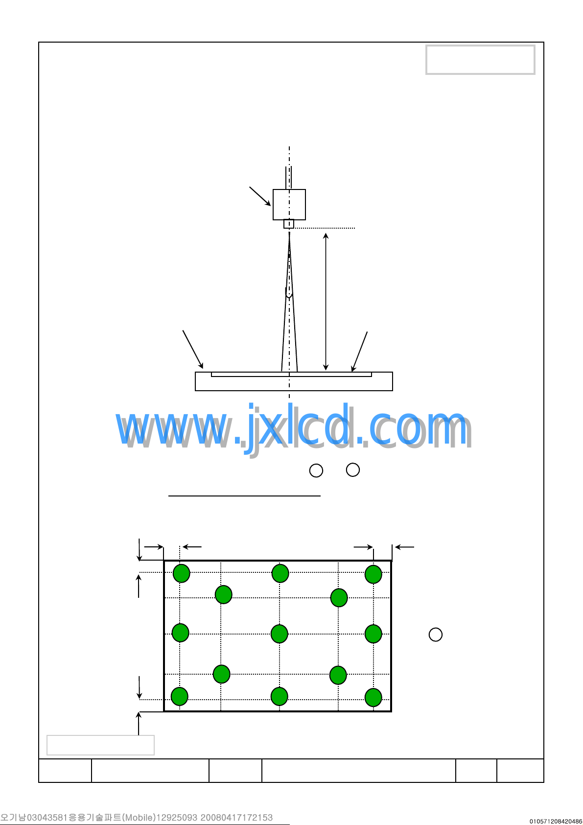
Note 5) After stabilizing and leaving the panel alone at a given temperature for 30 min , the measurement
should be executed. Measurement should be executed in a stable, windless,and dark room.
30 min after lighting the backlight. This should be measured in the center of screen.
Lamp current : 6.0mA ( Inverter : SIC-130T )
Environment condition : Ta = 25 ± 2 °C
Photo-detector
( TOPCON BM-5A
PR-650 )
Field
= 1°
50 cm
TFT-LCD module
Center of the screen
[ Optical characteristics measurement setup ]
www.jxlcd.com
www.jxlcd.com
Note 6) Definition of 13 points white variation (
Maximum luminance of 13 points
δL=
Minimum luminance of 13 points
10mm
10mm
13 12
256 512
10
δ
L
1 13
), [ ~ ]
768
LCD panel
10mm
11
9
192
8
5
3
10mm
SEC Secret
Doc.No. Rev.No Page / 30LTN150PF-L04 9
7
4
2
05-A00-S-080417
6
384
576
(lines)
1
: test point
3. ELECTRICAL CHARACTERISTICS
Approval
3.1 TFT LCD MODULE
Voltage of Power Supply
Differential Input
Voltage for LVDS
Receiver Threshold
Hsync Frequency
Main Frequency
Rush Current
Current of Power
Supply
High
White
Max
Pattern
Low
DD
IH
IL
H
DCLK
RUSH
I
DD
Ta = 25 ± 2֠°C
NoteUnitMax.Typ.Min.SymbolItem
V3.63.33.0V
V
CM
= +1.2VmV+100--V
mV---100V
Hz-60-fvVsync Frequency
KHz-63.98-f
MHz-54-f
(4)A1.5--I
(2),(3)*amA-430(2),(3)*bmA-450-Mosaic
(2),(3)*cmA600550-
Note (1) Display data pins and timing signal pins should be connected.(GND=0V)
(2) fV=60Hz, f
(3) Power dissipation pattern
www.jxlcd.com
*a) White Pattern *b) Mosaic Pattern
VIEW AREA
www.jxlcd.com
DCLK
=54MHZ, Vdd = 3.3V , DC Current.
Display Brightest Gray Level
Display Darkest Gray Level
SEC Secret
Doc.No. Rev.No Page / 30LTN150PF-L04 10
05-A00-S-080417
 Loading...