

Samsung LTN-141W1-L09 Datasheet
Approval
Approval
TO
DATE
SAMSUNG TFT-LCD
SAMSUNG TFT-LCD
MODEL NO. : LTN141W1-L09
MODEL NO. : LTN141W1-L09
NOTE :
www.jxlcd.com
: Dell /Compal
: July, 9, 2007
- Extension code [ -1 ] ; LTN141W1-L09-1
www.jxlcd.com
- Surface type [ Anti-Glare ]
Any Modification of Specification is not allowed without SEC's Permission.
APPROVED BY :
PREPARED BY : LCD Product Planning Group 1, Marketing Team
SAMSUNG ELECTRONICS CO., LTD.
Samsung Secret
Doc.No. Rev.No
W. B . Youn
04-A02-S-070709
Page
/ 32LTN141W1-L09
1
CONTENTS
Approval
Approval
Revision History
General Description
1. Absolute Maximum Ratings
1.1 Absolute Ratings of environment
1.2 Electrical Absolute Ratings
2. Optical Characteristics
3. Electrical Characteristics
3.1 TFT LCD Module
3.2 Backlight Unit
3.3 Inverter
4. Block Diagram
4.1 TFT LCD Module
4.2 Backlight Unit
4.3 Inverter Unit
5. Input Terminal Pin Assignment
5.1 Input Signal & Power
5.2 LVDS Interface
5.3 Backlight Unit
www.jxlcd.com
5.4 Timing Diagrams of LVDS For Transmitting
5.5 Input Signals, Basic Display Colors and Gray Scale of Each Color.
5.6 Pixel format
5.7 Inverter Signals & Power
www.jxlcd.com
-------------------( 3 )
-------------------( 4 )
-------------------( 5 )
-------------------( 7 )
-------------------( 10 )
-------------------( 14 )
-------------------( 16 )
6. Interface Timing
6.1 Timing Parameters
6.2 Timing Diagrams of interface Signal
6.3 Power ON/OFF Sequence
7. Outline Dimension
8. Packing
9. Markings & Others
10. General Precaution
11. EDID
Samsung Secret
Doc.No. Rev.No
-------------------( 22 )
-------------------( 24 )
------------------- ( 25 )
------------------- ( 26 )
-------------------( 28)
-------------------( 30)
04-A02-S-070709
Page
/ 32LTN141W1-L09
2
REVISION HISTORY
REVISION HISTORY
. The preliminary specification of LTN141W1-L09 was first issued.AllP00June 16, 2006
Approval
Approval
SummaryPageRev. No.Date
1P01April 13, 2007
. The extension code was changed from 0 to 1.
change : new PCB version for WWAN
. The approval specification was issued.AllA00May. 31. 2007
. SMBUS Value of EDID was modified.32A01June.18.2007
. SMBUS Value of EDID was modified.32A02July . 9. 2007
www.jxlcd.com
www.jxlcd.com
Samsung Secret
Doc.No. Rev.No
04-A02-S-070709
Page
/ 32LTN141W1-L09
3
Approval
Approval
GENERAL DESCRIPTION
DESCRIPTION
LTN141W1-L09 is a color active matrix TFT (Thin Film Transistor) liquid crystal display
(LCD) that uses amorphous silicon TFT as a switching devices. This model is composed of
a TFT LCD panel, a driver circuit and a backlight unit. The resolution of a 14.1" contains
1,280 x 800 pixels and can display up to 262,144 colors. 6 O'clock direction is the Optimum
viewing angle.
FEATURES
• High contrast ratio, high aperture structure
• 1280 x 800 pixels resolution
• Low power consumption
• Fast Response
• Single CCFL
• DE(Data enable) only mode
• 3.3V LVDS Interface
• Onboard EEDID chip
• Attached Burst mode Inverter with Ambient Light Sensor
APPLICATIONS
• Notebook PC
• If the usage of this product is not for PC application, but for others, please contact SEC.
www.jxlcd.com
www.jxlcd.com
GENERAL INFORMATION
Display area
Driver element
Display colors
Number of pixel
Pixel arrangement
Pixel pitch
a-Si TFT active matrix
262,144
RGB vertical stripe
mm303.36(H) x 189.6(V) (14.1” diagonal )
mm0.2370(H) x 0.2370(V) (TYP.)
NoteUnitSpecificationItem
16 : 10pixel1280 x RGB(3) x 800
Display Mode
Surface treatment
Samsung Secret
Doc.No. Rev.No
Normally white
Haze 25, Hard-Coating 3H
04-A02-S-070709
Page
/ 32LTN141W1-L09
4
Mechanical Information
Approval
Approval
Module
size
Weight
1. ABSOLUTE MAXIMUM RATINGS
1.1 ENVIRONMENTAL ABSOLUTE RATINGS
Operating temperate
(Temperature of glass surface)
Max.
320.0
206.0
5.5
440
455
NoteUnitTyp.Min.Item
mm319.5319.0Horizontal (H)
w/o inverter ass’y
mm205.5205.0Vertical (V)
mm--Depth (D)
w/o Inverterg390-
w/ Inverter assemblyg405-
NoteUnitMax.Min.SymbolItem
(1)°C60-20 TSTGStorage temperate
(1)°C500TOPR
(2),(4)G240-SnopShock ( non-operating )
Note (1) Temperature and relative humidity range are shown in the figure below.
95 % RH Max. (40 °C ≥ Ta)
Maximum wet - bulb temperature at 39
www.jxlcd.com
www.jxlcd.com
100
-40 -20 0 20 40 60 80
Relative Humidity ( %RH)
90
80
60
40
20
Operating Range
Storage Range
5
0
Temperature (
(2) 2ms, half sine wave, one time for ±X, ±Y, ± Z.
(3) 5 - 500 Hz, random vibration, 30min for X, Y, Z.
(4) At testing Vibration and Shock, the fixture in holding the Module to be tested have to be
hard and rigid enough so that the Module would not be twisted or bent by the fixture.
O
C or less. (Ta > 40 °C ) No condensation
( 40,90 )
( 50,50.4 )
( 60,27.7 )
O
C)
(3),(4)G2.41-VnopVibration (non-operating)
Samsung Secret
Doc.No. Rev.No
04-A02-S-070709
Page
/ 32LTN141W1-L09
5
1.2 ELECTRICAL ABSOLUTE RATINGS
(1) TFT LCD MODULE
Approval
Approval
DD =3.3V, VSS = GND = 0V
V
NoteUnitMax.Min.SymbolItem
DDPower Supply Voltage
Note (1) Within Ta (25 ± 2 °C)
(2) BACK-LIGHT UNIT
LLamp Current
Note 1) Permanent damage to the device may occur if maximum values are exceeded
Functional operation should be restricted to the conditions described under normal operating conditions.
www.jxlcd.com
www.jxlcd.com
(1)V3.6VSS - 0.3V
Ta = 25 ± 2 °C
NoteUnitMax.Min.SymbolItem
(1)mArms7.02.0I
(1)kHz8040FLLamp frequency
Samsung Secret
Doc.No. Rev.No
04-A02-S-070709
Page
/ 32LTN141W1-L09
6
Approval
Approval
2. OPTICAL CHARACTERISTICS
The following items are measured under stable conditions. The optical characteristics
should be measured in a dark room or equivalent state with the methods shown in Note (5).
Measuring equipment : TOPCON BM-5A and PR-650
* Ta = 25 ± 2 °C, VDD=3.3V, fv= 60Hz, fDCLK = 68.9MHz, IL = 6.0 mArms
Contrast Ratio
(5 Points)
Response Time at Ta
( Rising + Falling )
Average Luminance
of White (5 Points)
Red
Color
Chromaticity
( CIE )
Green
Blue
www.jxlcd.com
www.jxlcd.com
White
CR
RT_B/W
L,AVE
Y
Y
X
W
Y
Normal
Viewing
Angle
φ = 0
θ = 0
Unit
-
msec
-220200Y
(0.610)(0.590)(0.570)RX
(0.360)(0.340)(0.320)R
(0.340)(0.320)(0.300)GX
(0.560)(0.540)(0.520)G
(0.175)(0.155)(0.135)BX
(0.160)(0.140)(0.120)BY
(0.335)(0.315)(0.295)W
(0.350)(0.330)(0.310)
cd/m
-
2
NoteMaxTyp.Min.ConditionSymbolItem
(1), (2), (5)--300
(1), (3)3525-T
I
L=6.0mA
(1), (4)
(1), (5)
PR-650
Color Gamut
L
θ
Hor.
R
CR ≥ 10
Ver.
θL
L
R
L
L
CR ≥ 100
Viewing
Angle
Hor.
Ver.
13 Points
White Variation
Samsung Secret
Doc.No. Rev.No
2520
2520θ
105φH
2015φ
04-A02-S-070709
-4542
-5040
-5040θ
-2515φH
-4030φ
%
Degrees
Degrees
-
Page
(1), (5)
BM-5A
(6)2.2--δ
7
/ 32LTN141W1-L09
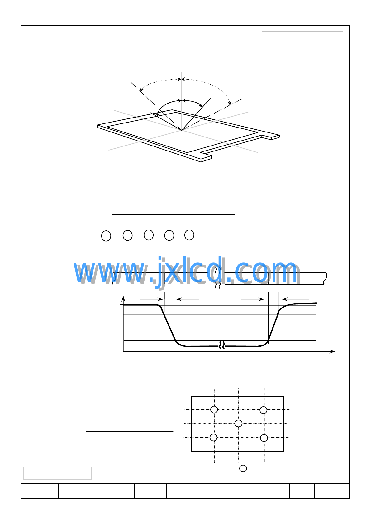
Note 1) Definition of Viewing Angle : Viewing angle range( 10
Normal Line
o
φ = 0
,
θ = 0
θ L
φ L
L
=90
o
x
θ
φ H
≤ C/R, 100 ≤ C/R )
o
θ R
y
Approval
Approval
12 O’clock
direction
φ
H
= 90
o
6 O’clock
direction
φ
Note 2) Definition of Contrast Ratio (CR) : Ratio of gray max (Gmax) ,gray min (Gmin)
at 5 points(4, 5, 7, 9, 10)
Points : , , , , at the figure of Note (6).
Note 3) Definition of Response time :
Display data
Optical
Response
o
= 90
L
CR(4) + CR(5) + CR(7) + CR(9) + CR(10)
CR =
4 9
www.jxlcd.com
www.jxlcd.com
100%
90%
10%
0%
5
White(TFT OFF) White(TFT OFF)
7
5
10
Black(TFT ON)
TR
x'y'
=90
θ
R
TF
o
Note 4) Definition of Average Luminance of White : measure the luminance of white at 5 points.
(320) ( 640) (960)
5
L,AVE )
10
7
5
04-A02-S-070709
9
4
: test point
Average Luminance of White ( Y
Y
L4 + YL5 + YL7 + YL9 + YL10
YL,AVE =
Samsung Secret
Doc.No. Rev.No
Time
VIEW AREA
(200)
(400)
(600)
(lines)
Page
/ 32LTN141W1-L09
8
Approval
Approval
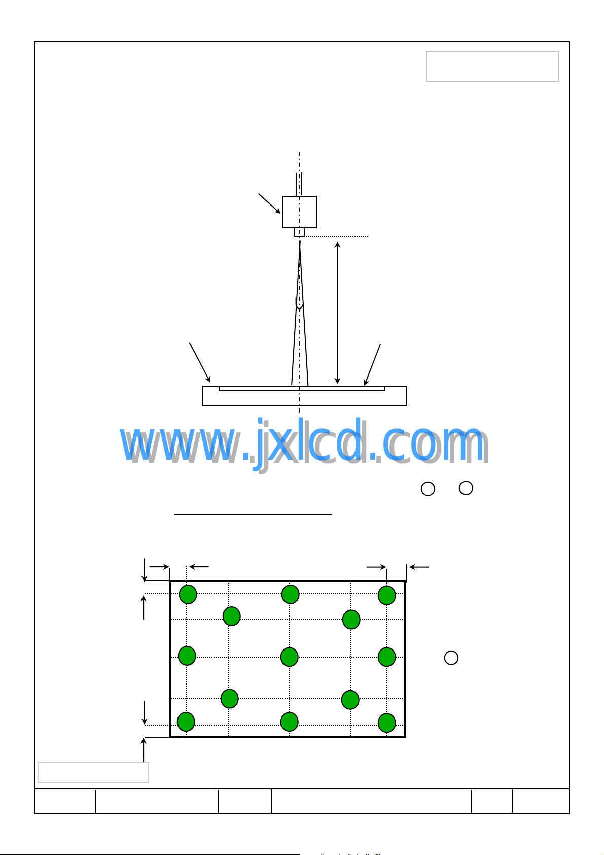
Note 5) After stabilizing and leaving the panel alone at a given te mperature for 30 min , the measurement
should be executed. Measurement should be executed in a stable, windless,and dark room.
30 min after lighting the backlight. This should be measured in the center of screen.
Lamp current : 6.0mA
Environment condition : Ta = 25 ± 2 °C
Photo-detector
( TOPCON BM-5A
PR-650 )
Field
= 2°
50 cm
TFT-LCD module
Center of the screen
[ Optical characteristics measurement setup ]
www.jxlcd.com
www.jxlcd.com
Note 6) Definition of 13 points white variation (δ L ), CR variation( CVER ) [ ~ ]
Maximum luminance of 13 points
δ L =
10mm
Minimum luminance of 13 points
10mm
320 640
13 12
10
960
9
LCD panel
113
10mm
11
200
8
5
3
10mm
Samsung Secret
Doc.No. Rev.No
7
4
2
04-A02-S-070709
6
400
600
(lines)
1
: test point
Page
/ 32LTN141W1-L09
9
3. ELECTRICAL CHARACTERISTICS
3.1 TFT LCD MODULE
Approval
Approval
Ta= 25 ± 2°C
NoteUnitMax.Typ.Min.SymbolItem
DDVoltage of Power Supply
Differential Input
Voltage for LVDS
Receiver Threshold
White
Current of Power
Supply
Note (1) Display data pins and timing signal pins should be connected.( GND = 0V )
V = 60Hz, fDCLK = 68.9MHZ, VDD = 3.3V , DC Current.
(2) f
(3) Power dissipation pattern
www.jxlcd.com
www.jxlcd.com
*a) White Pattern *b) Mosaic Pattern
ILLow
HHsync Frequency
DCLKMain Frequency
RUSHRush Current
DD
I
V3.63.33.0V
V
CM = +1.2VmV+100--VIHHigh
mV---100V
Hz-60-fvVsync Frequency
fv*816KHz-48.96-f
fh*1408MHz-68.93-f
(4)A1.5--I
(2),(3)*amA-290(2),(3)*bmA-300-Mosaic
(2),(3)*cmA485350-V. stripe
VIEW AREA
Samsung Secret
Doc.No. Rev.No
Display Brightest Gray Level
Display Darkest Gray Level
04-A02-S-070709
Page
10
/ 32LTN141W1-L09
 Loading...