

Page 1
Global LCD Panel Exchange Center
www.panelook.com
Approval Specification
Approval Specification
Customer : General
SAMSUNG TFT--
SAMSUNG TFT
SAMSUNG TFT-LCD
MODEL : :
MODEL
MODEL : LTM230TT01
Any Modification of Specification is not allowed without SEC's Permission.
NOTE :
LCD
LCD
LTM230TT01
LTM230TT01
DATE : 10 / Jul / 2008
Customer’’
Customer
SIGNATURE
s Approval
s Approval
DATE
PREPARED BY
APPROVAED BY
DATE
10/Jul/’08
DATE
10/Jul /’08
Application Engineering Part 1(HD) , LCD Business
Samsung Electronics Co . , LTD.
1/40Page05-000-G-080710Doc. NoLTM230TT01MODEL
One step solution for LCD / PDP / OLED panel application: Datasheet, inventory and accessory!
www.panelook.com
Page 2
Global LCD Panel Exchange Center
Contents
Revision History -------------------------------------------------------------------------------------- (3)
General Description --------------------------------------------------------------------------------- (4)
1. Absolute Maximum Ratings ------------------------------------------------------------------- (5)
2. Optical Characteristics -------------------------------------------------------------------------- (7)
3. Electrical Characteristics ------------------------------------------------------------------------(12)
3.1 TFT LCD Module
3.2 Back Light Unit
4. Block Diagram ----------------------------------------------------------------------------------- (17)
4.1 TFT LCD Module
4.2 Back Light Unit
www.panelook.com
Approval Specification
Approval Specification
5. Input Terminal Pin Assignment -------------------------------------------------------------- (18)
5.1 Input Signal & Power
5.2 LVDS Interface
5.3 Input Signals, Basic Display Colors and Gray Scale of Each Color
6. Interface Timing --------------------------------------------------------------------------------- (26)
6.1 Timing Parameters (DE only mode)
6.2 Timing Diagrams of interface Signal (DE only mode)
6.3 Power ON/OFF Sequence
6.4 VDD Power Dip Condition
7. Outline Dimension ------------------------------------------------------------------------------- (31)
8. Reliability Test ------------------------------------------------------------------------------------ (34)
9. Packing -------------------------------------------------------------------------------------------- (35)
10. Marking & Others ------------------------------------------------------------------------------- (36)
11. General Precaution ---------------------------------------------------------------------------- (38)
11.1 Handling
11.2 Storage
11.3 Operation
11.4 Others
One step solution for LCD / PDP / OLED panel application: Datasheet, inventory and accessory!
2/40Page05-000-G-080710Doc. NoLTM230TT01MODEL
www.panelook.com
Page 3
Global LCD Panel Exchange Center
* Revision History
www.panelook.com
Approval Specification
Approval Specification
Date
2008
Rev.
No
SummaryPage
Approval specification of LTM230TT01 model was issued first.all000Jul. 10,
One step solution for LCD / PDP / OLED panel application: Datasheet, inventory and accessory!
3/40Page05-000-G-080710Doc. NoLTM230TT01MODEL
www.panelook.com
Page 4
Global LCD Panel Exchange Center
General Description
www.panelook.com
Approval Specification
Approval Specification
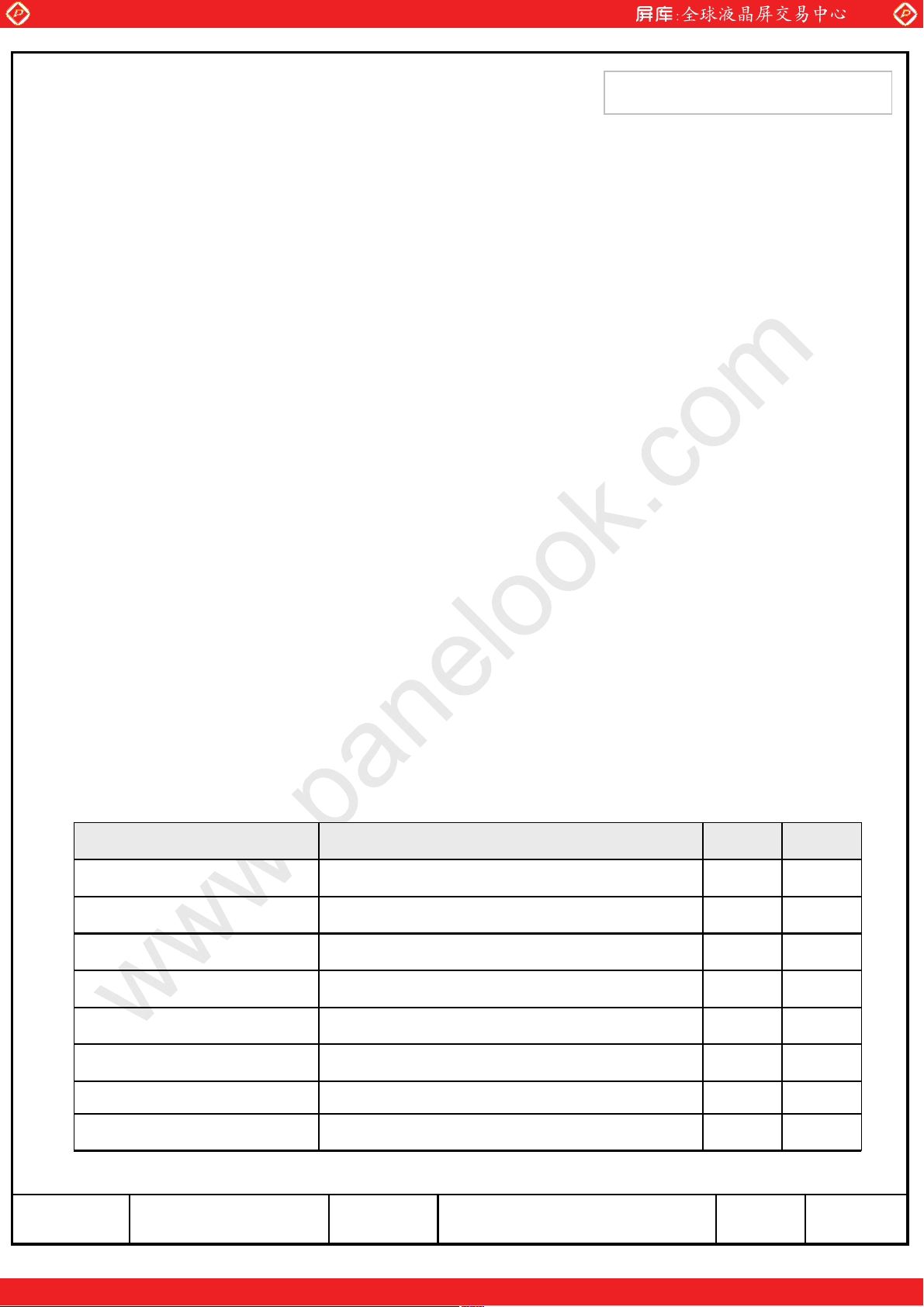
Description
LTM230TT01 is a color active matrix liquid crystal display (LCD) that uses amorphous
silicon TFT (Thin Film Transistor) as switching components. This model is composed of
a TFT LCD panel, a driver circuit and a back light unit. The resolution of a 23” is 2048 x
1152 and this model can display up to 16.7 millions colors.
Features
High contrast ratio, high aperture structure
TN (Twisted Nematic) mode
Wide Viewing Angle
High speed response
WDXGA (2048 x 1152 pixels) resolution
Low power consumption
DE (Data Enable) only mode
LVDS (Low Voltage Differential Signaling) interface (2pixel/clock)
Compact Size Design
RoHS, TCO 03’ compliance
Applications
Workstation & desktop monitors
Display terminals for AV application products
Monitors for industrial machine
* If the module is used to other applications besides the above, please contact SEC
in advance.
General Information
Haze 25% , Hard coating (3H)Surface Treatment
UnitSpecificationItems
mm0.249(H) x 0.249(W)Pixel Pitch
mm509.952(H) x 286.848(V)Active Display Area
colors16.7M (Hi-FRC)Display Colors
pixel2,048 x 1,152Number of Pixels
RGB vertical stripePixel Arrangement
Note
Normally WhiteDisplay Mode
cd/༇300(Typ.)Luminance of White
One step solution for LCD / PDP / OLED panel application: Datasheet, inventory and accessory!
4/40Page05-000-G-080710Doc. NoLTM230TT01MODEL
www.panelook.com
Page 5
Global LCD Panel Exchange Center
Mechanical Information
www.panelook.com
Approval Specification
Approval Specification
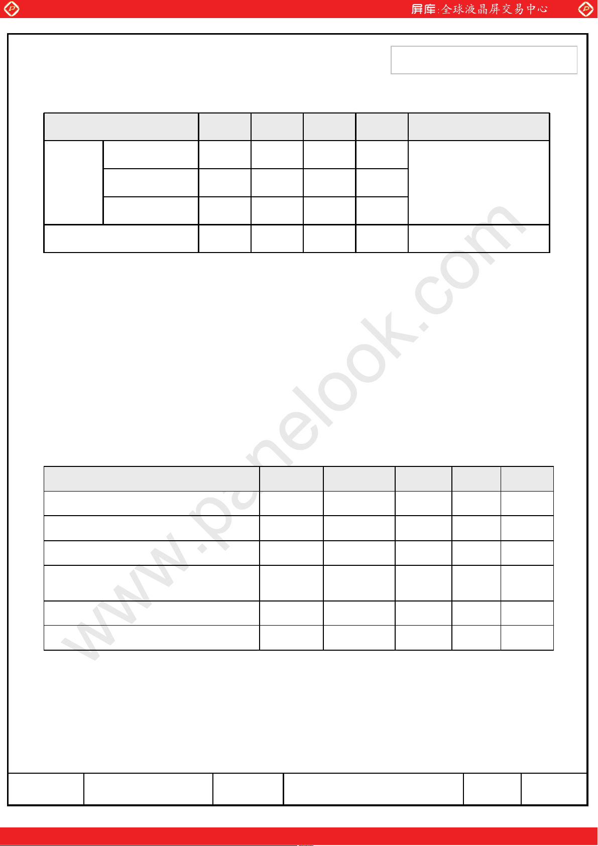
Max.
534.5
mm534.0533.5Horizontal (H)
Module
312.2
mm311.7311.2Vertical (V) w/o inverter ass’y
size
18.9
mm--Depth (D)
3,050
Note (1) Mechanical tolerance is · 0.5mm unless there is a special comment.
1. Absolute Maximum Ratings
NoteUnitTyp.Min.Item
LCD module onlyg--Weight
If the condition exceeds maximum ratings, it can cause malfunction or unrecoverable
damage to the device.
NoteUnitMax.Min.SymbolItem
Power Supply Voltage
Data Signal
Storage temperature
Center of Glass surface temperature
(Operation)
Shock ( non - operating )
Vibration ( non - operating )
Note (1) Ta= 25 · 2 ¶C
DD
sig
STG
OPR
nop
nop
V5-V
60-25T
500T
(1)V6.5GND-0.5V
(2)
(2)
(3)(5)G50-S
(4)(5)G1.5-V
One step solution for LCD / PDP / OLED panel application: Datasheet, inventory and accessory!
5/40Page05-000-G-080710Doc. NoLTM230TT01MODEL
www.panelook.com
Page 6
Global LCD Panel Exchange Center
www.panelook.com
Approval Specification
Approval Specification
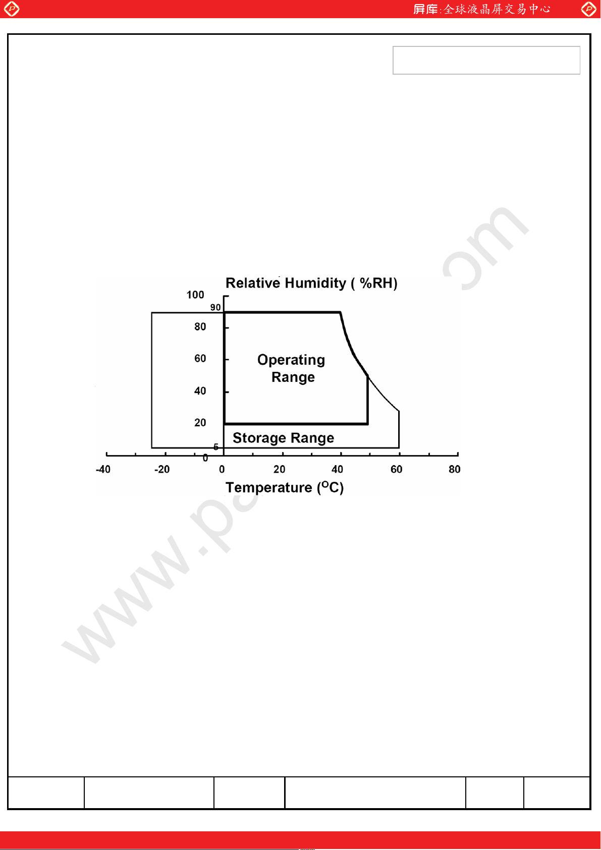
(2) Temperature and relative humidity range are shown in the figure below.
a. 90 % RH Max. (Ta ˺ 39 ¶C)
b. Maximum wet-bulb temperature at 39 ¶C or less. (Ta ˺ 39 ¶C)
c. No condensation
(3) 11ms, sine wave, one time for ·X, ·Y, ·Z axis
(4) 10-300 Hz, Sweep rate 10min, 30min for X,Y,Z axis
(5) At vibration and shock test, the fixture which holds the module to be tested has to be
hard and rigid enough so that the module would not be twisted or bent by the fixture.
(39,90)
(39,90)
(50,50.4)
(50,50.4)
25,5)
((--25,5)
Fig. Temperature and Relative humidity range
(60,27.7)
(60,27.7)
One step solution for LCD / PDP / OLED panel application: Datasheet, inventory and accessory!
6/40Page05-000-G-080710Doc. NoLTM230TT01MODEL
www.panelook.com
Page 7
Global LCD Panel Exchange Center
2. Optical Characteristics
www.panelook.com
Approval Specification
Approval Specification
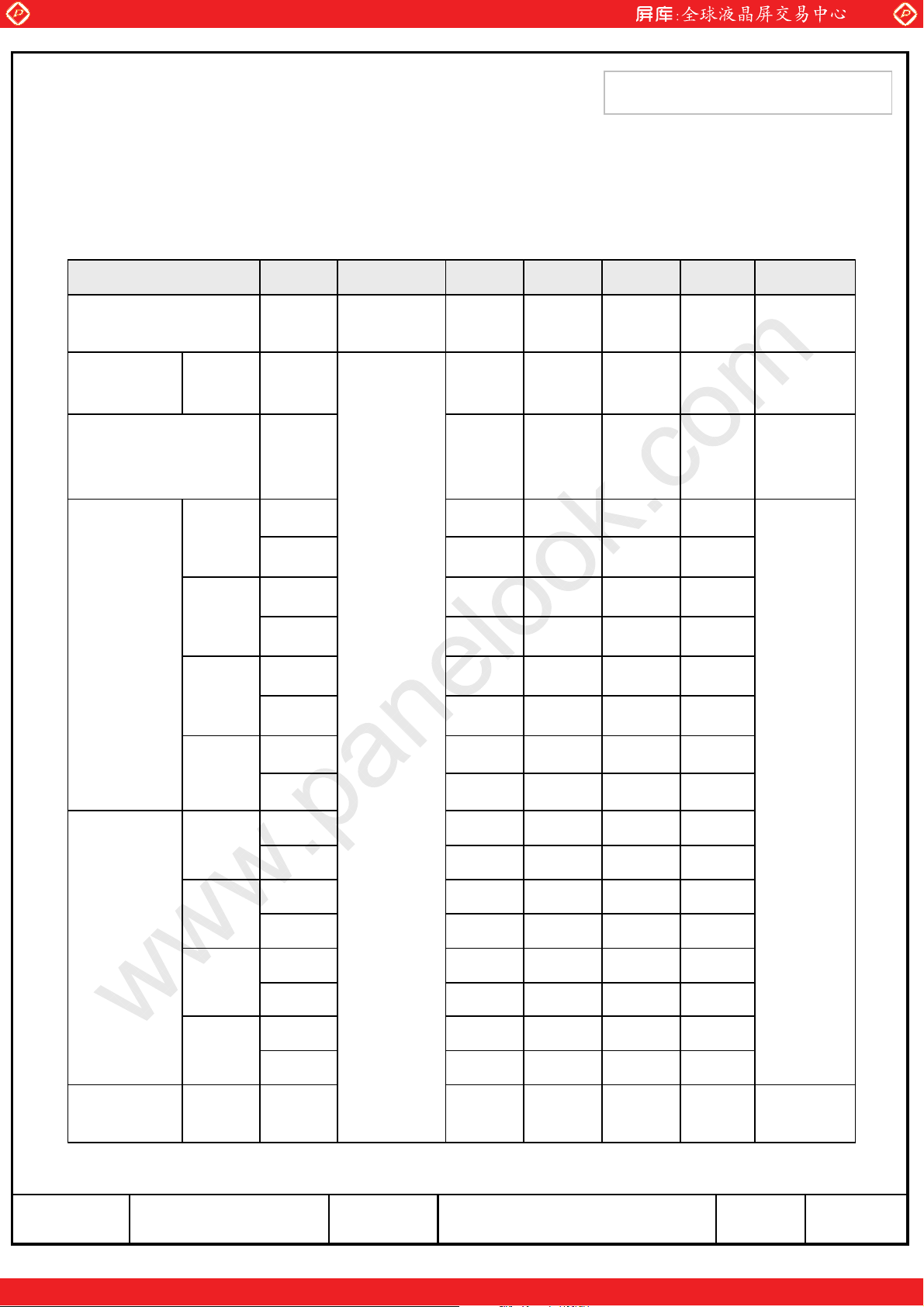
The optical characteristics should be measured in a dark room or equivalent.
Measuring equipment : SR-3, RD-80S (TOPCON), EZ-Contrast (Eldim)
(Ta = 25 · 2¶C, VDD=5V, fv= 60Hz, fDCLK=78.5MHz, IL = 7.5mArms)
NoteUnitMax.Typ.Min.ConditionSymbolItem
Contrast Ratio
(Center of screen)
Response
Time(On/Off)
Luminance of White
(Center of screen)
Green
Color
Chromaticity
(CIE 1931)
Red
Blue
White
Red
-1000600C/R
105-Tr + TfOn/Off
L
Normal
ɂ
ɂ
Viewing
Angle
-300250Y
0.6700.6400.610Rx
0.3600.3300.300Ry
0.3300.3000.270Gx
0.6300.6000.570Gy
0.1800.1500.120Bx
0.0900.0600.030By
0.3430.3130.283Wx
0.3590.3290.299Wy
-0.451-Ru'
-0.523-Rv'
msec
cd/m
2
(3)
SR-3
(5)
RD-80S
(6)
SR-3
(7),(8)
SR-3
-0.125-Gu'
Color
Chromaticity
(CIE 1976)
C.G.L
(ACC ONLY)
* C.G.L : Color Grayscale Linearity
One step solution for LCD / PDP / OLED panel application: Datasheet, inventory and accessory!
Green
-0.564-Gv'
-0.175-Bu'
Blue
-0.158-Bv'
-0.198-Wu'
White
-0.468-Wv'
Ƹu'v'White
(9)0.02--
7/40Page05-000-G-080710Doc. NoLTM230TT01MODEL
www.panelook.com
Page 8
Global LCD Panel Exchange Center
www.panelook.com
Approval Specification
Approval Specification
NoteUnitMax.Typ.Min.ConditionSymbolItem
%-72--Color Gamut
K-6500--Color Temperature
ɂ
Hor.
Viewing
Angle
Ver.
Brightness Uniformity
(9 Points)
L
ɂ
R
ɂ
U
ɂ
D
uni
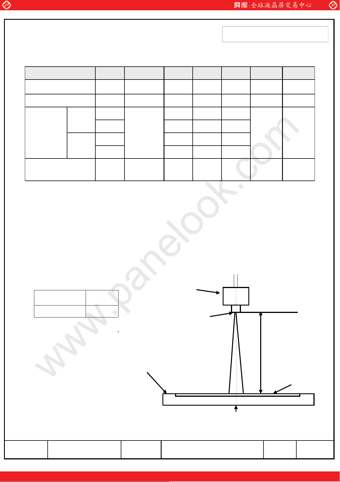
Note (1) Test Equipment Setup
The measurement should be executed in a stable, windless and dark room between
30min after lighting the back light at the given temperature for stabilization
of the back light. This should be measured in the center of screen.
Single lamp current : 7.5mA
Environment condition : Ta = 25 · 2 ¶C
CR˻10
-8070
-8070
Degrees
-8070
-8070
%25--B
(8)
EZ-
Contrast
(4)
SR-3
Field Photo detector
2ദSR-3
TFT - LCD Module
Photo detector
Field
SR-3 : 40
RD-80S : 50
LCD Panel
The center of the screen
8/40Page05-000-G-080710Doc. NoLTM230TT01MODEL
One step solution for LCD / PDP / OLED panel application: Datasheet, inventory and accessory!
www.panelook.com
Page 9
Global LCD Panel Exchange Center
B
G
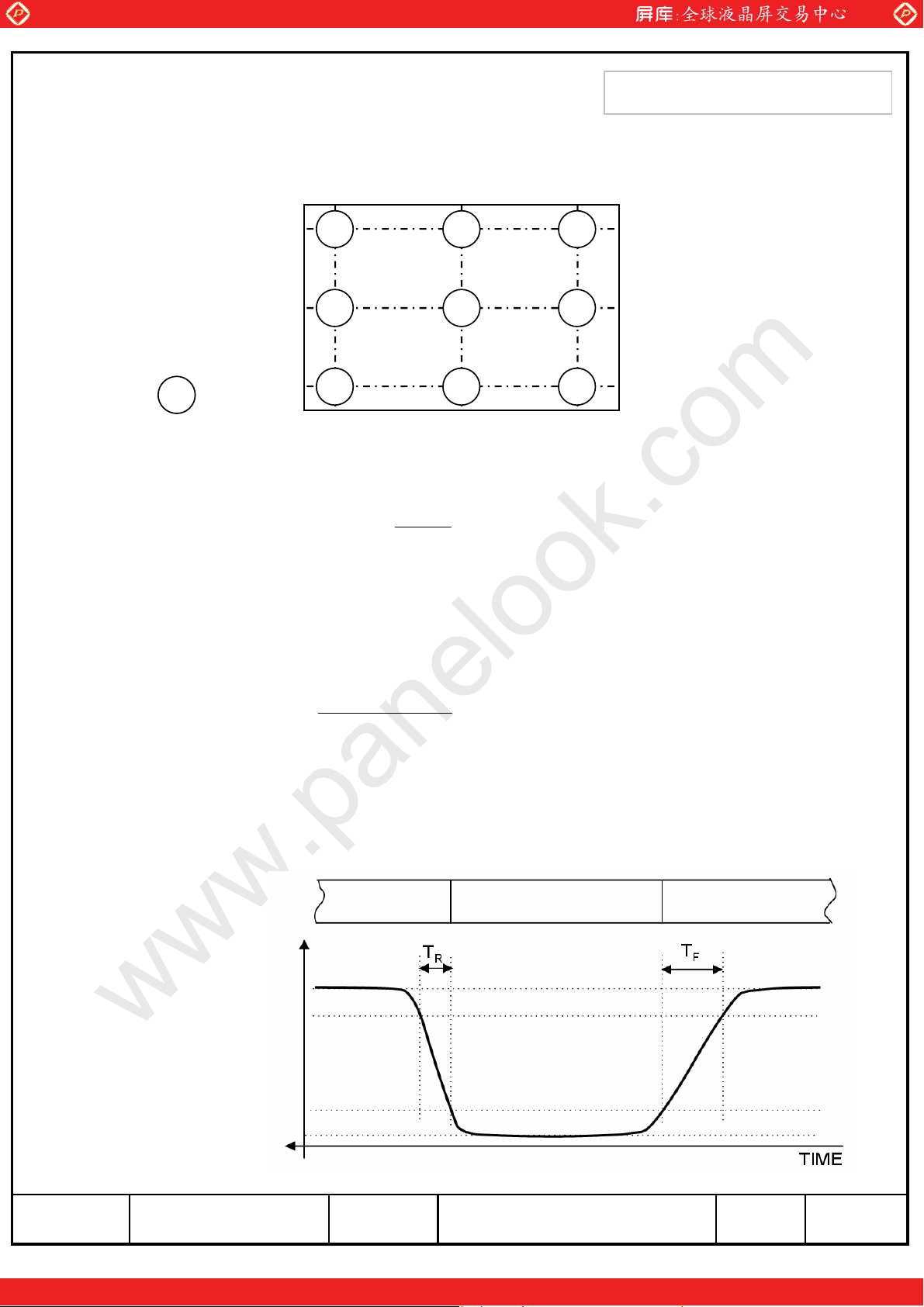
Note (2) Definition of test point
www.panelook.com
512 1024 1536
Approval Specification
Approval Specification
Active Area
6
: Test Point
Note (3) Definition of Contrast Ratio (C/R)
: Ratio of gray max (Gmax) & gray min (Gmin) at the center point㽶 of the panel
3 2 1
G
CR
=
max
8 79
45
288
576
864
min
Gmax : Luminance with all pixels white
Gmin : Luminance with all pixels black
Note (4) Definition of 9 points brightness uniformity
Buni
BB
=×
100
(max min)
−
max
Bmax : Maximum brightness
Bmin : Minimum brightness
Note (5) Definition of Response time : Sum of Tr, Tf
Display Data White(TFT off) Black(TFT on) White(TFT off)
Optical Instruments
Response
100%
90%
10%
0%
One step solution for LCD / PDP / OLED panel application: Datasheet, inventory and accessory!
9/40Page05-000-G-080710Doc. NoLTM230TT01MODEL
www.panelook.com
Page 10
Global LCD Panel Exchange Center
Note (6) Definition of Luminance of White : Luminance of white at center point㽶
Note (7) Definition of Color Chromaticity (CIE 1931, CIE1976)
Color coordinate of Red, Green, Blue & White at center point㽶
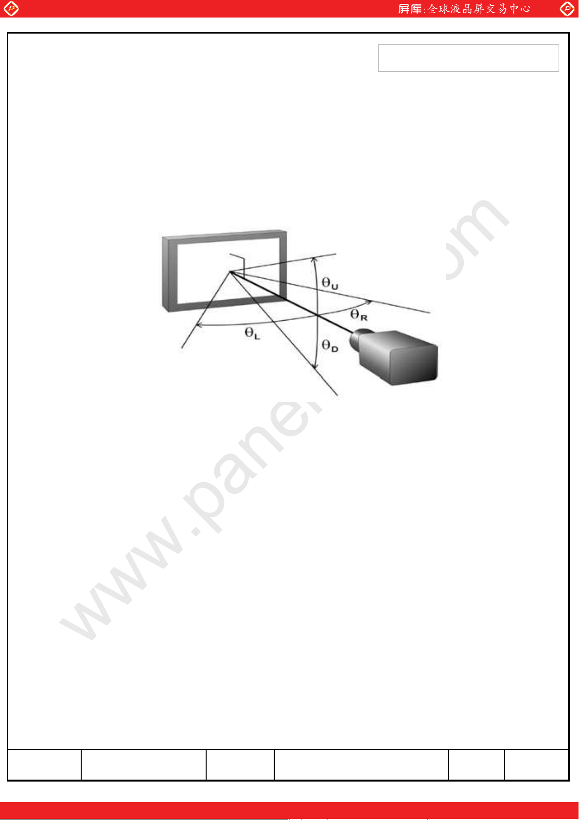
Note (8) Definition of Viewing Angle
: Viewing angle range (CR ˻ 10,5)
www.panelook.com
Approval Specification
Approval Specification
One step solution for LCD / PDP / OLED panel application: Datasheet, inventory and accessory!
10/40Page05-000-G-080710Doc. NoLTM230TT01MODEL
www.panelook.com
Page 11
Global LCD Panel Exchange Center
www.panelook.com
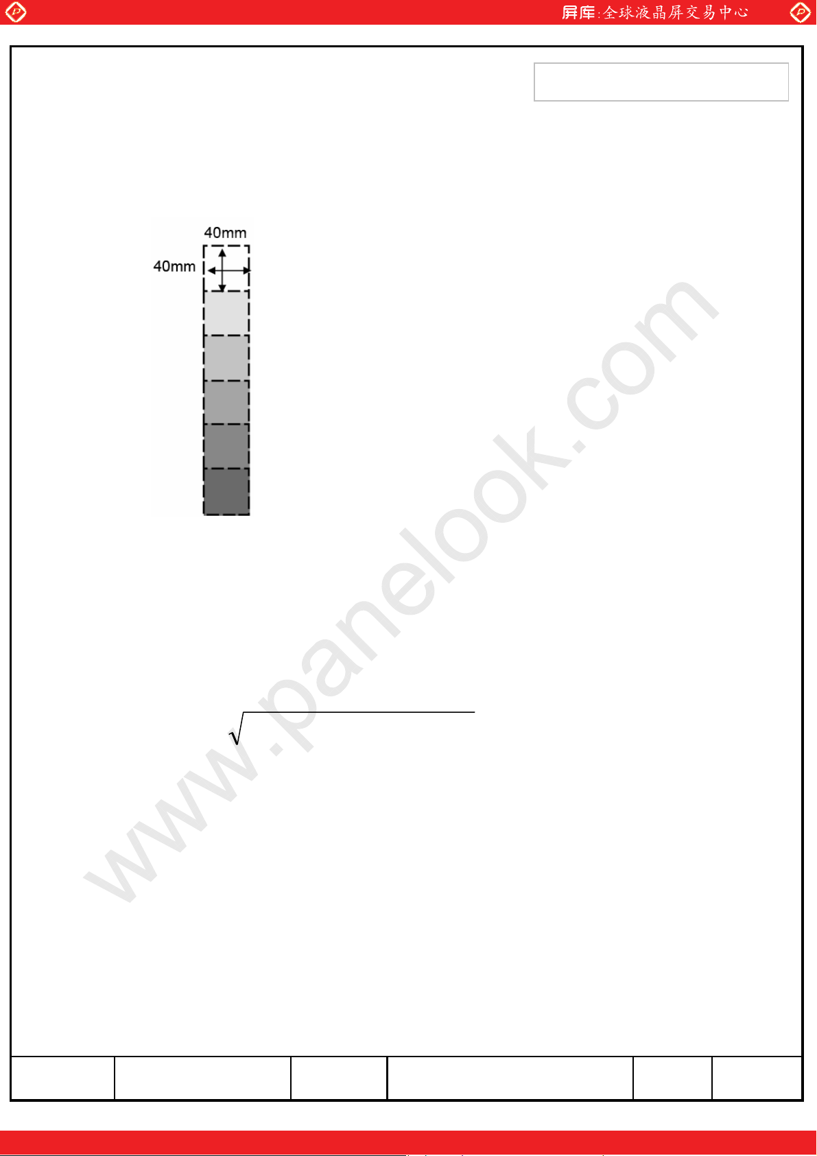
Note (9) Color Grayscale Linearity
a. Test image : 100% full white pattern with a test pattern as below
b. Test pattern : Squares, 40mm by 40mm in size, filled with 255, 225, 195, 165, 135 and
105 grays steps should be arranged at the centerྜྷ of the screen.
Approval Specification
Approval Specification
c. Test method
st
gray step : move a square of 255 gray level should be moved into the center of the
-1
screen and measure luminance and u’ and v’ coordinates.
- Next gray step : Move a 225 gray square into the center and measure both
luminance and coordinates, too.
d. Test evaluation
Δu' v'= (u' - u' ) + (v' - v' )
AB
2
AB
2
Where A, B : 2 gray levels found to have the largest color differences between them
i.e. get the largest ȟu’ and ȟv’ of each 6 pair of u’ and v’ and calculate the ȟu’v’.
One step solution for LCD / PDP / OLED panel application: Datasheet, inventory and accessory!
11/40Page05-000-G-080710Doc. NoLTM230TT01MODEL
www.panelook.com
Page 12
Global LCD Panel Exchange Center
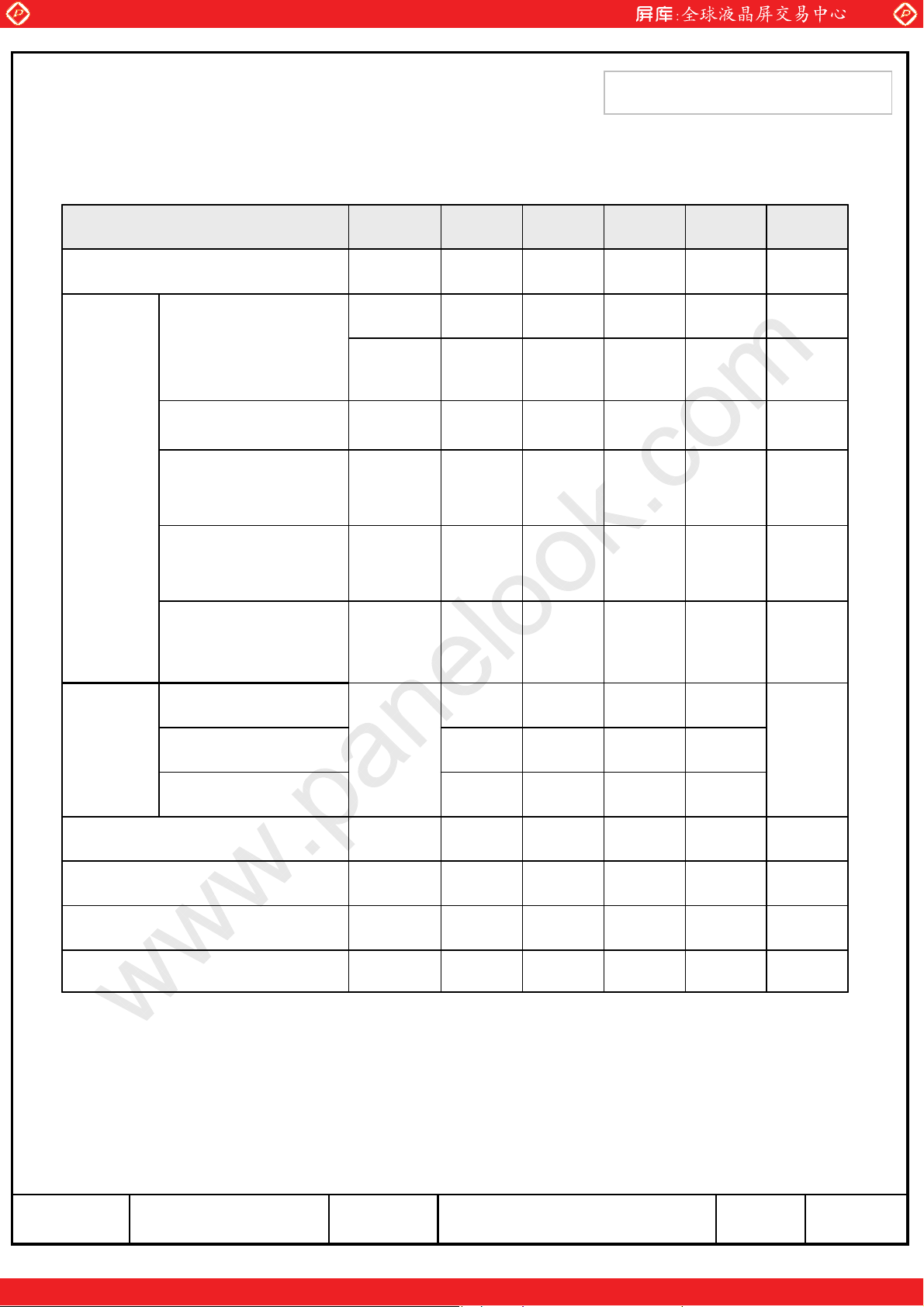
3. Electrical Characteristics
3.1 TFT LCD Module
The connector for display data & timing signal should be connected.
www.panelook.com
Approval Specification
Approval Specification
Ta = 25¶C
NoteUnitMax.Typ.Min.SymbolItem
Voltage of Power Supply
Differential Input
Voltage for LVDS
Receiver Threshold
LVDS skew
LVDS
Input
Characteri
Differential input
voltage
stics
Input voltage range
(single-ended)
Common mode
voltage
(a) Black
Current of
Power
Supply
DD
SKEW
IN
V
CM
I
DD
|V
0+
ID
|/2
1.2
2.4-
|V
(1)V5.55.04.5V
(2)mV+100--High
mV---100Low
(3)ps300-300t
(4)mV600200|VID|
(4)V2.40V
(4)V
|/2
ID
mA-1,600-
mA-1,100-(b) White (5),(6)
mA2,0001,800-(c) Dot
Vsync Frequency
Hsync Frequency
Main Frequency
Rush Current
V
H
DCLK
RUSH
Note (1) The ripple voltage should be controlled under 10% of VDD.
Hz626049f
kHz73.57157.8f
MHz8178.563.8f
(7)A5.0--I
12/40Page05-000-G-080710Doc. NoLTM230TT01MODEL
One step solution for LCD / PDP / OLED panel application: Datasheet, inventory and accessory!
www.panelook.com
Page 13
Global LCD Panel Exchange Center
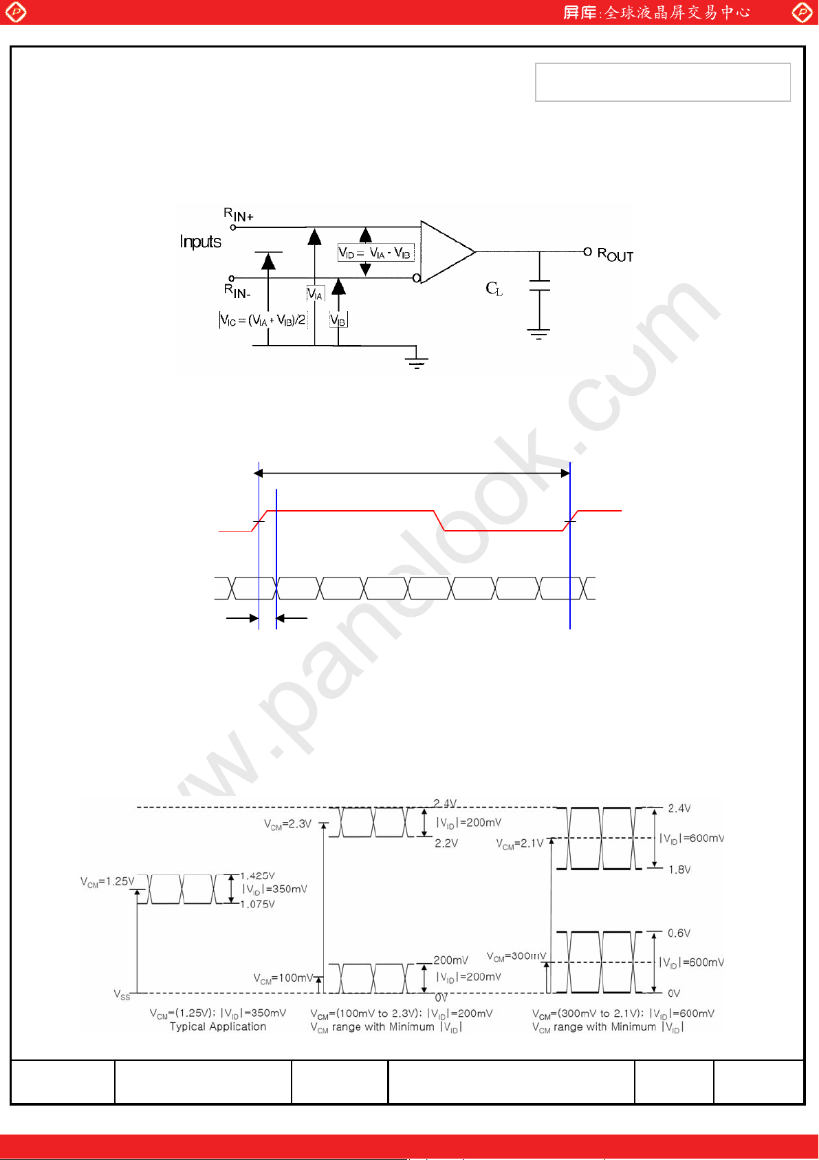
(2)
Differential receiver voltage definitions and propagation delay and transition time test
www.panelook.com
circuit
a. All input pulses have frequency = 10MHz, t
b. C
includes all probe and fixture capacitance
L
or tF=1ns
R
Note a.
Note b.
(3) LVDS Receiver DC parameters are measured under static and steady conditions
which may not be reflective of its performance in the end application.
Approval Specification
Approval Specification
T
LVDS Clk
V
= 0V
DIFF
LVDS Data
RX +/-
t
SKEW
where tskew : skew between LVDS clock & LVDS data,
T : 1 period time of LVDS clock
cf) (-/+) of 300psec means LVDS data goes before or after LVDS clock.
(4) Definition of V
and V
ID
using single-end signals
CM
= 0V
V
DIFF
Differential
Differential
One step solution for LCD / PDP / OLED panel application: Datasheet, inventory and accessory!
13/40Page05-000-G-080710Doc. NoLTM230TT01MODEL
www.panelook.com
Page 14
Global LCD Panel Exchange Center
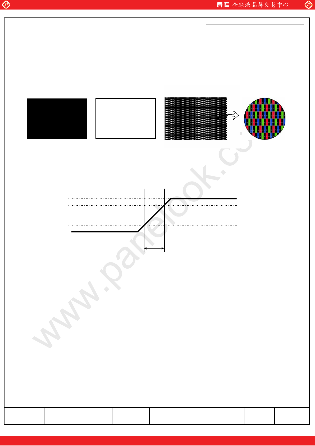
(5) fV=60Hz, fDCLK = 78.5MHz, VDD = 5.0V, DC Current.
(6) Power dissipation check pattern (LCD Module only)
a) Black Pattern b) White Pattern c) Dot Pattern
www.panelook.com
Approval Specification
Approval Specification
(7) Measurement Condition
100%
90%
10%
GND
Rush Current I
RUSH
T
=470༕
RUSH
can be measured when T
. is 470༕.
RUSH
V
DD
One step solution for LCD / PDP / OLED panel application: Datasheet, inventory and accessory!
14/40Page05-000-G-080710Doc. NoLTM230TT01MODEL
www.panelook.com
Page 15
Global LCD Panel Exchange Center
www.panelook.com
Approval Specification
Approval Specification
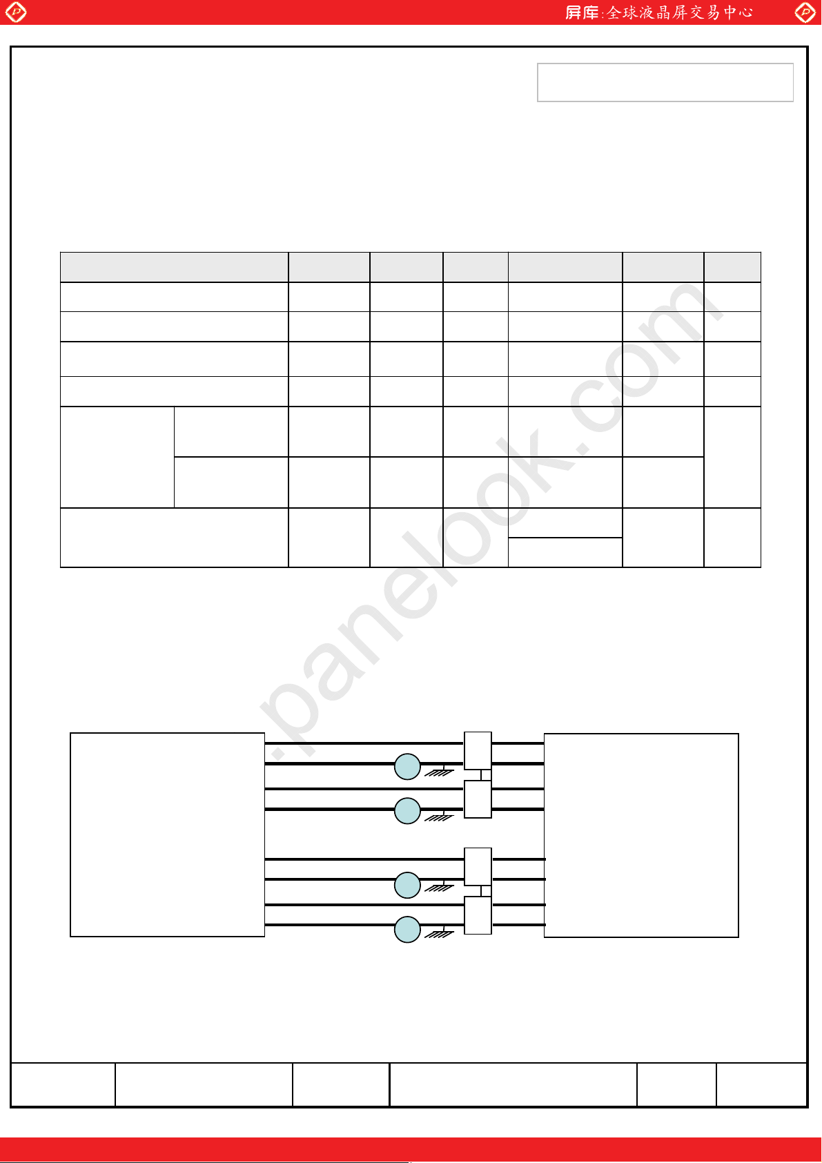
3.2 Back Light Unit
The back light unit is an edge - lighting type with 2 dual CCFTs ( Cold Cathode
Fluorescent Tube ) The characteristics of two dual lamps are shown in the following tables.
Ta=25 · 2¶C
NoteUnitMax.Typ.Min.SymbolItem
Lamp Current
Lamp Voltage
Lamp Frequency
Asymmetry
Inverter
waveform
Note (1) Specified values are for a single lamp.
Lamp current is measured with current meter for high frequency as shown below.
Refer to the following block diagram of the back light unit for more information.
rate
Distortion
rate
L
L
L
(1)mArms8.07.54.0I
Vrms-850-V
(2)kHz80-40f
(3)Hour--50,000HrOperating Life Time
%10--Wasy
(4)
1.55541.4141.2726Wdis
0 : 1,800
--VsStartup Voltage
25: 1,450
(5)Vrms
LCD Module
HOT(RED)
COLD(WHITE)
HOT(BLUE)
COLD(GRAY)
HOT(RED)
COLD(WHITE)
HOT(BLUE)
COLD(GRAY)
I
1
A
I
2
A
I
3
INVERTER
A
I
4
A
Fig. Measurement point of Lamp Current
(SI1700)
15/40Page05-000-G-080710Doc. NoLTM230TT01MODEL
One step solution for LCD / PDP / OLED panel application: Datasheet, inventory and accessory!
www.panelook.com
Page 16
Global LCD Panel Exchange Center
I
I
I
(2) Lamp frequency which may produce interference with horizontal synchronous
frequency may cause line flow on the display. Therefore lamp frequency should be
detached from the horizontal synchronous frequency and its harmonics as far as
possible in order to avoid interference.
(3) Life time (Hr) is defined as the time when brightness of a lamp unit itself becomes
50% or less than its original value at the condition of Ta = 25·2¶C and I
(4) Designing a system inverter intended to have better display performance, power
efficiency and lamp reliability.
They would help increase the lamp lifetime and reduce leakage current.
a. The measurement should be done at typical lamp current.
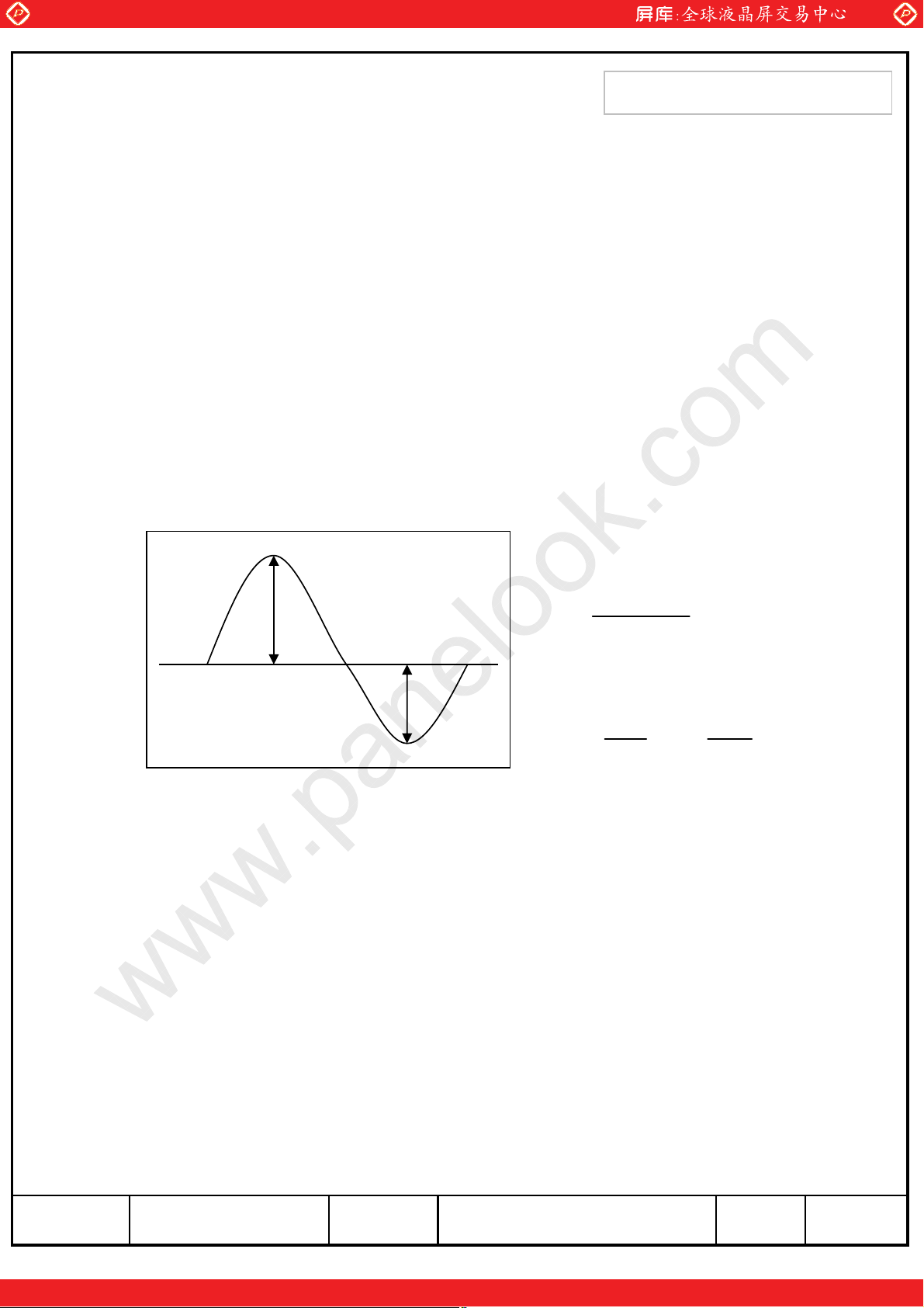
b. The asymmetry rate of the inverter waveform should be less than 10%.
c. The distortion rate of the waveform should be ˲2 with ·10% tolerance.
- Inverter output waveform had better be more similar to ideal sine wave.
www.panelook.com
Approval Specification
Approval Specification
= 7.5mArms
L
Asymmetry rate
p-p
||II
I
p
I
-p
Fig. Wave form of the inverter
(5) If an inverter has shutdown function, it should keep its output for over 1 second
even if the lamp connector is open. Otherwise the lamps may not be turned on.
Distortion rate
−
rms
p
I
||
rms
or
× 100
-p
I
||
rms
One step solution for LCD / PDP / OLED panel application: Datasheet, inventory and accessory!
16/40Page05-000-G-080710Doc. NoLTM230TT01MODEL
www.panelook.com
Page 17
Global LCD Panel Exchange Center
www.panelook.com
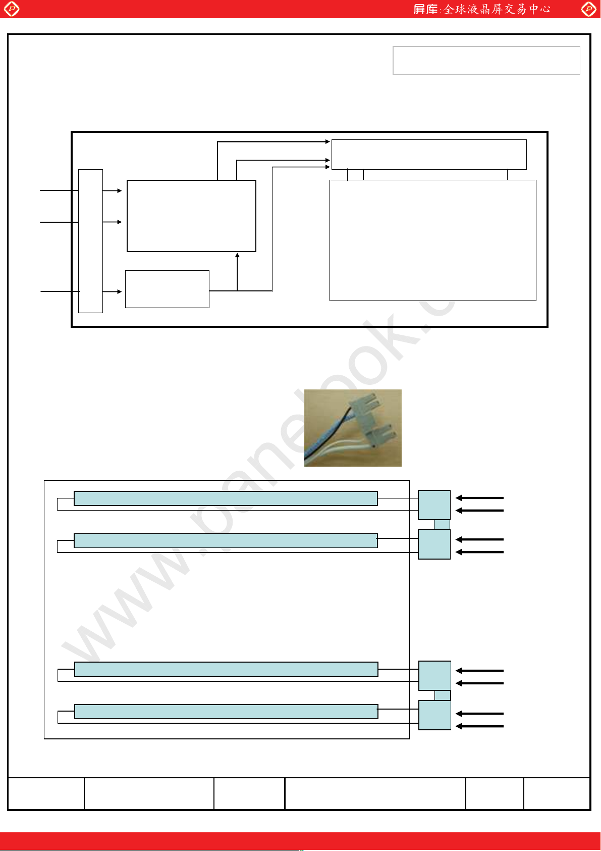
4. BLOCK DIAGRAM
4.1 TFT LCD Module
RSDS
Approval Specification
Approval Specification
LVDS
pair #1
LVDS
pair #2
+5.0V
V
DD
CN1
(30pin)
LVDS (Rx)
Timing Controller
Power
Circuit
4.2 Back Light Unit
LVDS(Tx)
RSDS(Tx)
Control signal
Source Driver ICs
S1 S2048
Control signal
Column Driver Circuit
TFT-LCD
(2048 x RGB x 1152 pixels)
Connector : YEON-HO 35001HS-04L
LAMP(CCFL)
LAMP(CCFL)
LAMP(CCFL)
LAMP(CCFL)
LAMP(CCFL)
LAMP(CCFL)
LAMP(CCFL)
LAMP(CCFL)
1
2
3
4
1
2
3
4
HOT(RED)
COLD(WHITE)
HOT(BLUE)
COLD(GRAY)
HOT(RED)
COLD(WHITE)
HOT(BLUE)
COLD(GRAY)
One step solution for LCD / PDP / OLED panel application: Datasheet, inventory and accessory!
17/40Page05-000-G-080710Doc. NoLTM230TT01MODEL
www.panelook.com
Page 18
Global LCD Panel Exchange Center
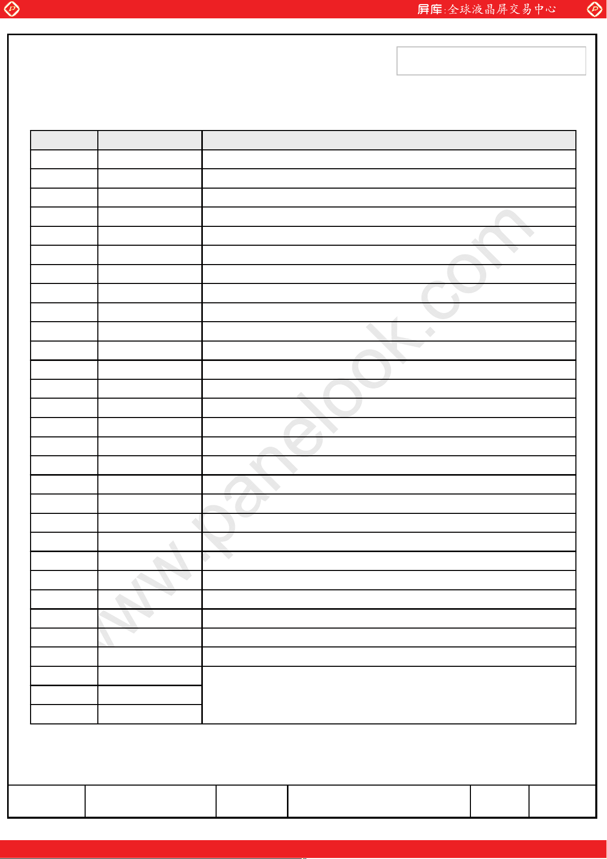
5. Input Terminal Pin Assignment
www.panelook.com
Approval Specification
Approval Specification
5.1. Input Signal & Power ( Connector : UJU IS100-L30O-C23 or Compatible )
FUNCTIONSYMBOLPIN NO
1
2
3
4
5
6
7
8
9
10
11
12
13
14
15
16
RXO0P
RXO1N
Negative LVDS differential data outputRXO0N
Positive LVDS differential data output
Negative LVDS differential data output
Positive LVDS differential data outputRXO1P
Negative LVDS differential data outputRXO2N
Positive LVDS differential data outputRXO2P
GroundGND
Negative Sampling Clock (ODD data)RXOC-
Positive Sampling Clock (ODD data)RXOC+
Negative LVDS differential data outputRXO3N
Positive LVDS differential data outputRXO3P
Negative LVDS differential data outputRXE0N
Positive LVDS differential data outputRXE0P
GroundGND
Negative LVDS differential data outputRXE1N
Positive LVDS differential data outputRXE1P
17
18
19
20
21
22
23
24
25
26
28
29
30
VDD
VDD
VDD
GroundGND
Negative LVDS differential data outputRXE2N
Positive LVDS differential data outputRXE2P
Negative Sampling Clock (EVEN data)RXEC-
Positive Sampling Clock (EVEN data)RXEC+
Negative LVDS differential data outputRXE3N
Positive LVDS differential data outputRXE3P
GroundGND
* CE (For LCD internal use only. Do not connect)NC
* CTL (For LCD internal use only. Do not connect)NC
No ConnectionNC27
Power Supply : +5V
* If the system already uses the 25, 26pins, it should keep under GND level
The voltage applied to those pins should not exceed -200mV.
One step solution for LCD / PDP / OLED panel application: Datasheet, inventory and accessory!
18/40Page05-000-G-080710Doc. NoLTM230TT01MODEL
www.panelook.com
Page 19
Global LCD Panel Exchange Center
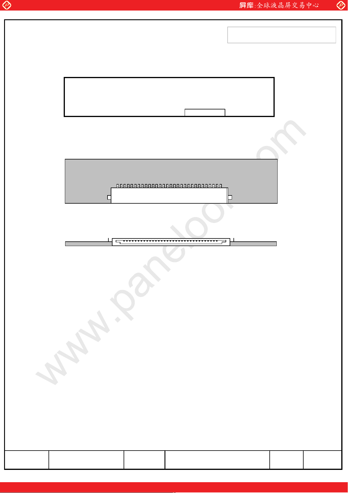
Note) Pin number starts from Left side
www.panelook.com
PCB
Pin No. 1 Pin No. 30
#30#1
Approval Specification
Approval Specification
UJU IS100-L30O-C23 or Compatible
#30#1
Fig. Connector diagram
a. All GND pins should be connected together and also be connected to the
LCD’s metal chassis.
b. All power input pins should be connected together.
c. All NC pins should be separated from other signal or power.
One step solution for LCD / PDP / OLED panel application: Datasheet, inventory and accessory!
19/40Page05-000-G-080710Doc. NoLTM230TT01MODEL
www.panelook.com
Page 20
Global LCD Panel Exchange Center
www.panelook.com
Approval Specification
Approval Specification
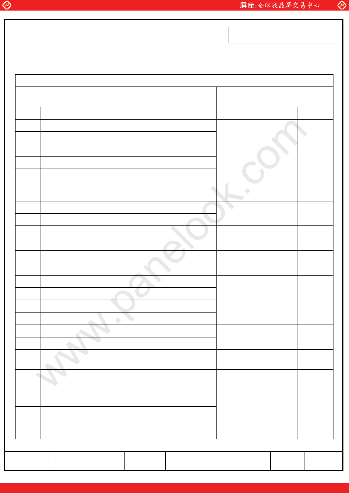
5.2 LVDS Interface
(1)
5.2.1 Odd Pixel Data (1st pixel data)
LVDS Transmitter ( DS90C383, DS90C385 ) Signal Interface
Device Input SignalDevice Input Pin
Red Odd Pixel Data (LSB) RO0TXIN0 51
Red Odd Pixel Data RO1TXIN1 52
Red Odd Pixel Data RO2TXIN2 54
Red Odd Pixel Data RO3TXIN3 55
Red Odd Pixel Data RO4TXIN4 56
Red Odd Pixel Data (MSB) RO7TXIN5 2
Red Odd Pixel Data RO5TXIN6 3
Green Odd Pixel Data (LSB)GO0TXIN7 4
Output
Signal
TXOUT0-
TXOUT0+
TXOUT3-
TXOUT3+
TXOUT0-
TXOUT0+
To LTM230TT01
Interface ( CN101 )
SymbolTerminalFunctionSymbolSymbolNo
No. 1
No. 2
No. 10
No. 11
No. 1
No. 2
RXO0-
RXO0+
RXO3-
RXO3+
RXO0-
RXO0+
Green Odd Pixel Data GO1TXIN8 6
Green Odd Pixel Data GO2TXIN9 7
Green Odd Pixel Data GO6TXIN108
Green Odd Pixel Data (MSB)GO7TXIN1110
Green Odd Pixel Data GO3TXIN1211
Green Odd Pixel Data GO4TXIN1312
Green Odd Pixel Data GO5TXIN1414
Blue Odd Pixel Data (LSB) BO0TXIN1515
Blue Odd Pixel Data BO6TXIN1616
Blue Odd Pixel Data (MSB) BO7TXIN1718
Blue Odd Pixel Data BO1TXIN1819
Blue Odd Pixel Data BO2TXIN1920
Blue Odd Pixel Data BO3TXIN2022
Blue Odd Pixel Data BO4TXIN2123
TXOUT1-
TXOUT1+
TXOUT3-
TXOUT3+
TXOUT1-
TXOUT1+
TXOUT3-
TXOUT3+
TXOUT1-
TXOUT1+
TXOUT2-
TXOUT2+
No. 3
No. 4
No. 10
No. 11
No. 3
No. 4
No. 10
No. 11
No. 3
No. 4
No. 5
No. 6
RXO1-
RXO1+
RXO3-
RXO3+
RXO1-
RXO1+
RXO3-
RXO3+
RXO1-
RXO1+
RXO2-
RXO2+
Blue Odd Pixel Data BO5TXIN2224
Red Odd Pixel Data RO6TXIN2750
One step solution for LCD / PDP / OLED panel application: Datasheet, inventory and accessory!
TXOUT3-
TXOUT3+
No. 10
No. 11
RXO3-
RXO3+
20/40Page05-000-G-080710Doc. NoLTM230TT01MODEL
www.panelook.com
Page 21
Global LCD Panel Exchange Center
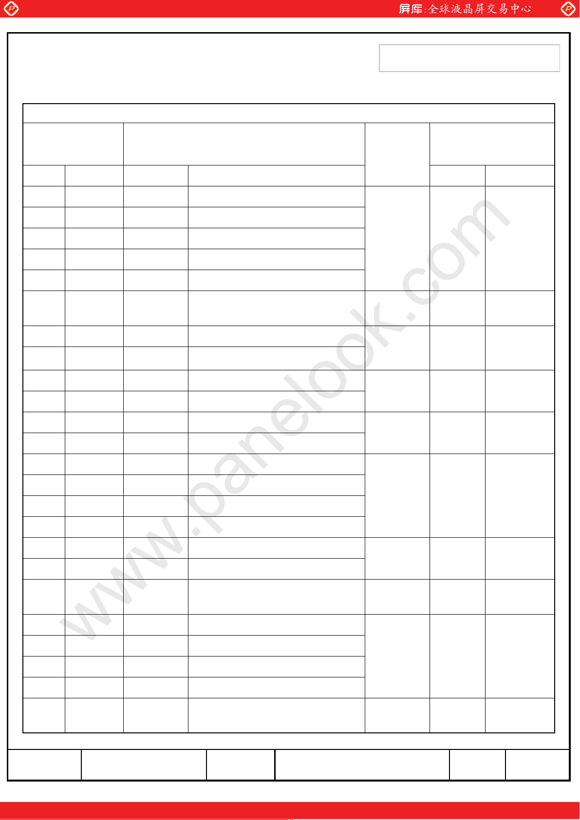
5.2.2 Even Pixel Data (2nd pixel data)
LVDS Transmitter ( DS90C383, DS90C385 ) Signal Interface
www.panelook.com
Approval Specification
Approval Specification
Device Input SignalDevice Input Pin
Red Even Pixel Data (LSB) RE0TXIN0 51
Red Even Pixel Data RE1TXIN1 52
Red Even Pixel Data RE2TXIN2 54
Red Even Pixel Data RE3TXIN3 55
Red Even Pixel Data RE4TXIN4 56
Red Even Pixel Data (MSB) RE7TXIN5 2
Red Even Pixel Data RE5TXIN6 3
Green Even Pixel Data (LSB)GE0TXIN7 4
Green Even Pixel Data GE1TXIN8 6
Green Even Pixel Data GE2TXIN9 7
Output
Signal
TXOUT0-
TXOUT0+
TXOUT3-
TXOUT3+
TXOUT0-
TXOUT0+
TXOUT1-
TXOUT1+
To LTM230TT01
Interface ( CN101 )
SymbolTerminalFunctionSymbolSymbolNo
No. 12
No. 13
No. 22
No. 23
No. 12
No. 13
No. 15
No. 16
RXE0-
RXE0+
RXE3-
RXE3+
RXE0-
RXE0+
RXE1-
RXE1+
Green Even Pixel Data GE6TXIN108
Green Even Pixel Data (MSB)GE7TXIN1110
Green Even Pixel Data GE3TXIN1211
Green Even Pixel Data GE4TXIN1312
Green Even Pixel Data GE5TXIN1414
Blue Even Pixel Data (LSB) BE0TXIN1515
Blue Even Pixel Data BE6TXIN1616
Blue Even Pixel Data (MSB) BE7TXIN1718
Blue Even Pixel Data BE1TXIN1819
Blue Even Pixel Data BE2TXIN1920
Blue Even Pixel Data BE3TXIN2022
Blue Even Pixel Data BE4TXIN2123
Blue Even Pixel Data BE5TXIN2224
TXOUT3-
TXOUT3+
TXOUT1-
TXOUT1+
TXOUT3-
TXOUT3+
TXOUT1-
TXOUT1+
TXOUT2-
TXOUT2+
No. 22
No. 23
No. 15
No. 16
No. 22
No. 23
No. 15
No. 16
No. 18
No. 19
RXE3-
RXE3+
RXE1-
RXE1+
RXE3-
RXE3+
RXE1-
RXE1+
RXE2-
RXE2+
Red Even Pixel Data RE6TXIN2750
One step solution for LCD / PDP / OLED panel application: Datasheet, inventory and accessory!
TXOUT3-
TXOUT3+
No. 22
No. 23
RXE3-
RXE3+
21/40Page05-000-G-080710Doc. NoLTM230TT01MODEL
www.panelook.com
Page 22
Global LCD Panel Exchange Center
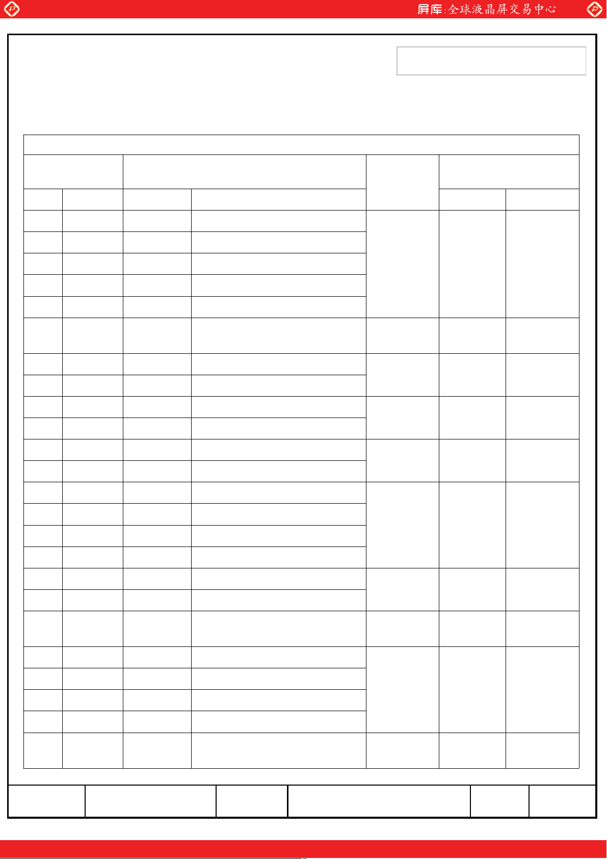
5.2 LVDS Interface (2)
5.2.3 Odd Pixel Data (1st pixel data)
LVDS Transmitter ( DS90C387 ) Signal Interface
www.panelook.com
Approval Specification
Approval Specification
Device Input SignalDevice Input Pin
Red Odd Pixel Data (LSB) RO0R1010
Red Odd Pixel Data RO1R119
Red Odd Pixel Data RO2R12 8
Red Odd Pixel Data RO3R13 7
Red Odd Pixel Data RO4R14 6
Red Odd Pixel Data (MSB) RO7R17 3
Red Odd Pixel Data RO5R15 5
Green Odd Pixel Data (LSB)GO0G10 2
Green Odd Pixel Data GO1G11 1
Green Odd Pixel Data GO2G12 100
Green Odd Pixel Data GO6G1694
Green Odd Pixel Data (MSB)GO7G1793
Output
Signal
A0M
A0P
A3M
A3P
A0M
A0P
A1M
A1P
A3M
A3P
To LTM230TT01
Interface ( CN101 )
SymbolTerminalFunctionSymbolSymbolNo
No. 1
No. 2
No. 10
No. 11
No. 1
No. 2
No. 3
No. 4
No. 10
No. 11
RXO0-
RXO0+
RXO3-
RXO3+
RXO0-
RXO0+
RXO1-
RXO1+
RXO3-
RXO3+
Green Odd Pixel Data GO3G1399
Green Odd Pixel Data GO4G1496
Green Odd Pixel Data GO5G1595
Blue Odd Pixel Data (LSB) BO0B1092
Blue Odd Pixel Data BO6B1686
Blue Odd Pixel Data (MSB) BO7B1785
Blue Odd Pixel Data BO1B1191
Blue Odd Pixel Data BO2B1290
Blue Odd Pixel Data BO3B1389
Blue Odd Pixel Data BO4B1488
Blue Odd Pixel Data BO5B1587
Red Odd Pixel Data RO6R164
A1M
A1P
A3M
A3P
A1M
A1P
A2M
A2P
A3M
A3P
No. 3
No. 4
No. 10
No. 11
No. 3
No. 4
No. 5
No. 6
No. 10
No. 11
RXO1-
RXO1+
RXO3-
RXO3+
RXO1-
RXO1+
RXO2-
RXO2+
RXO3-
RXO3+
One step solution for LCD / PDP / OLED panel application: Datasheet, inventory and accessory!
22/40Page05-000-G-080710Doc. NoLTM230TT01MODEL
www.panelook.com
Page 23
Global LCD Panel Exchange Center
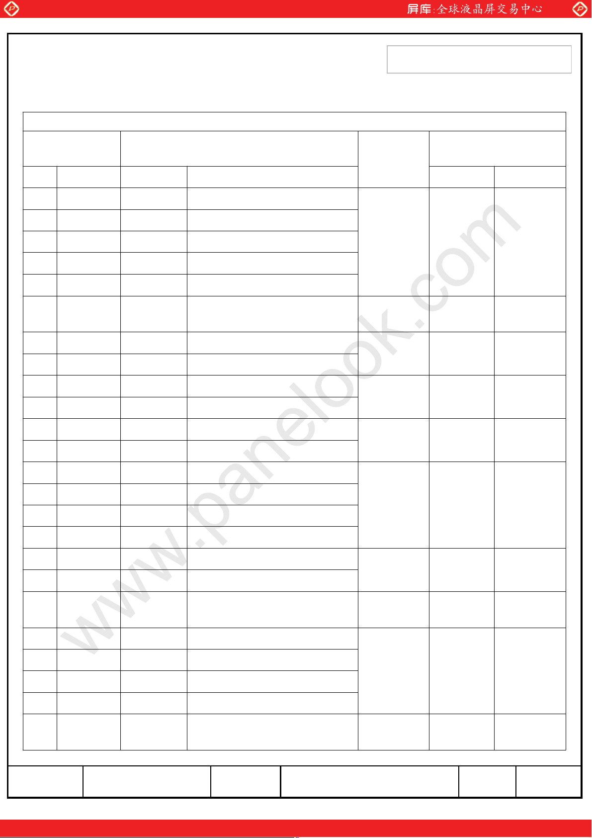
5.2.4 Even Pixel Data (2nd pixel data)
LVDS Transmitter ( DS90C387 ) Signal Interface
www.panelook.com
Approval Specification
Approval Specification
Device Input SignalDevice Input Pin
Red Even Pixel Data (LSB) RE0R2084
Red Even Pixel Data RE1R2181
Red Even Pixel Data RE2R22 80
Red Even Pixel Data RE3R23 79
Red Even Pixel Data RE4R24 78
Red Even Pixel Data (MSB) RE7R27 75
Red Even Pixel Data RE5R25 77
Green Even Pixel Data (LSB)GE0G20 74
Green Even Pixel Data GE1G21 73
Green Even Pixel Data GE2G22 72
Green Even Pixel Data GE6G2666
Green Even Pixel Data (MSB)GE7G2765
Output
Signal
A4M
A4P
A7M
A7P
A4M
A4P
A5M
A5P
A7M
A7P
To LTM230TT01
Interface ( CN101 )
SymbolTerminalFunctionSymbolSymbolNo
No. 12
No. 13
No. 22
No. 23
No. 12
No. 13
No. 15
No. 16
No. 22
No. 23
RXE0-
RXE0+
RXE3-
RXE3+
RXE0-
RXE0+
RXE1-
RXE1+
RXE3-
RXE3+
Green Even Pixel Data GE3G2371
Green Even Pixel Data GE4G2470
Green Even Pixel Data GE5G2569
Blue Even Pixel Data (LSB) BE0B2064
Blue Even Pixel Data BE6B2658
Blue Even Pixel Data (MSB) BE7B2757
Blue Even Pixel Data BE1B2163
Blue Even Pixel Data BE2B2262
Blue Even Pixel Data BE3B2361
Blue Even Pixel Data BE4B2460
Blue Even Pixel Data BE5B2559
Red Even Pixel Data RE6R2676
A5M
A5P
A7M
A7P
A5M
A5P
A6M
A6P
A7M
A7P
No. 15
No. 16
No. 22
No. 23
No. 15
No. 16
No. 18
No. 19
No. 22
No. 23
RXE1-
RXE1+
RXE3-
RXE3+
RXE1-
RXE1+
RXE2-
RXE2+
RXE3-
RXE3+
One step solution for LCD / PDP / OLED panel application: Datasheet, inventory and accessory!
23/40Page05-000-G-080710Doc. NoLTM230TT01MODEL
www.panelook.com
Page 24
Global LCD Panel Exchange Center
www.panelook.com
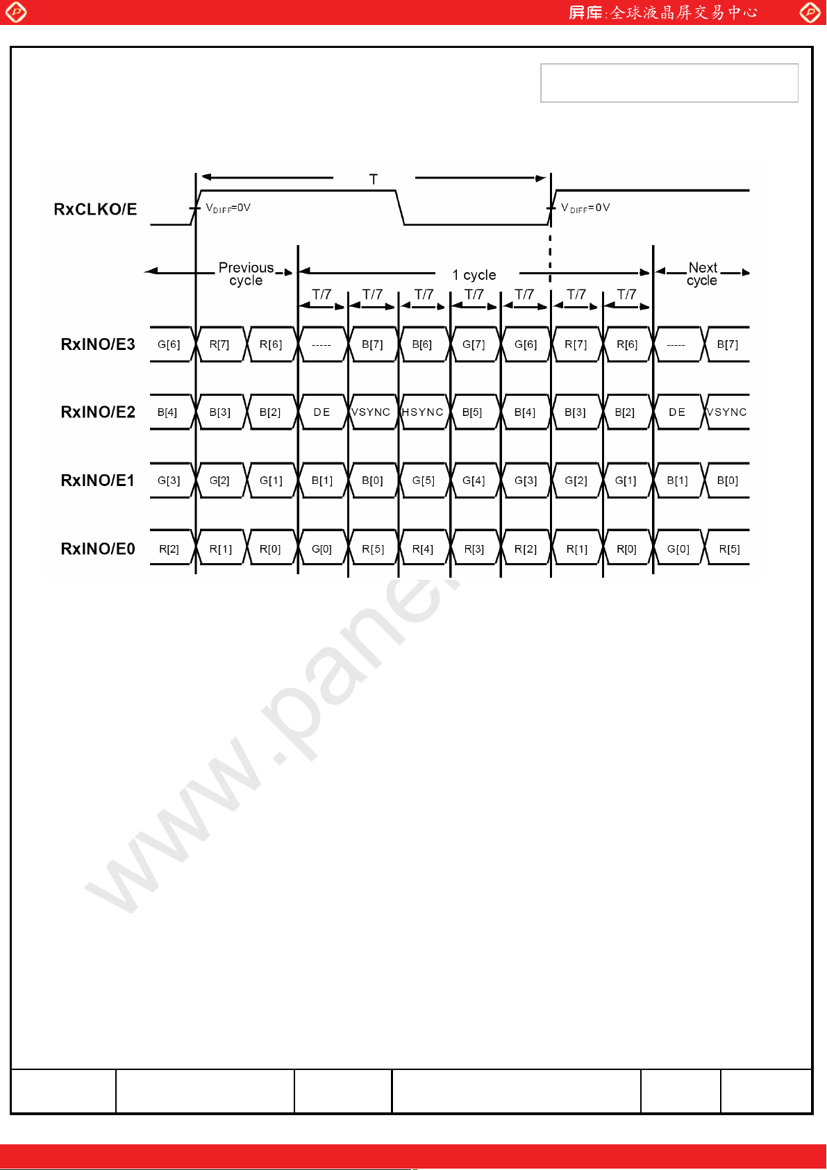
5.2.5 Timing Diagrams of LVDS For Transmitting
LVDS Receiver : Integrated T-CON
Approval Specification
Approval Specification
One step solution for LCD / PDP / OLED panel application: Datasheet, inventory and accessory!
24/40Page05-000-G-080710Doc. NoLTM230TT01MODEL
www.panelook.com
Page 25
Global LCD Panel Exchange Center
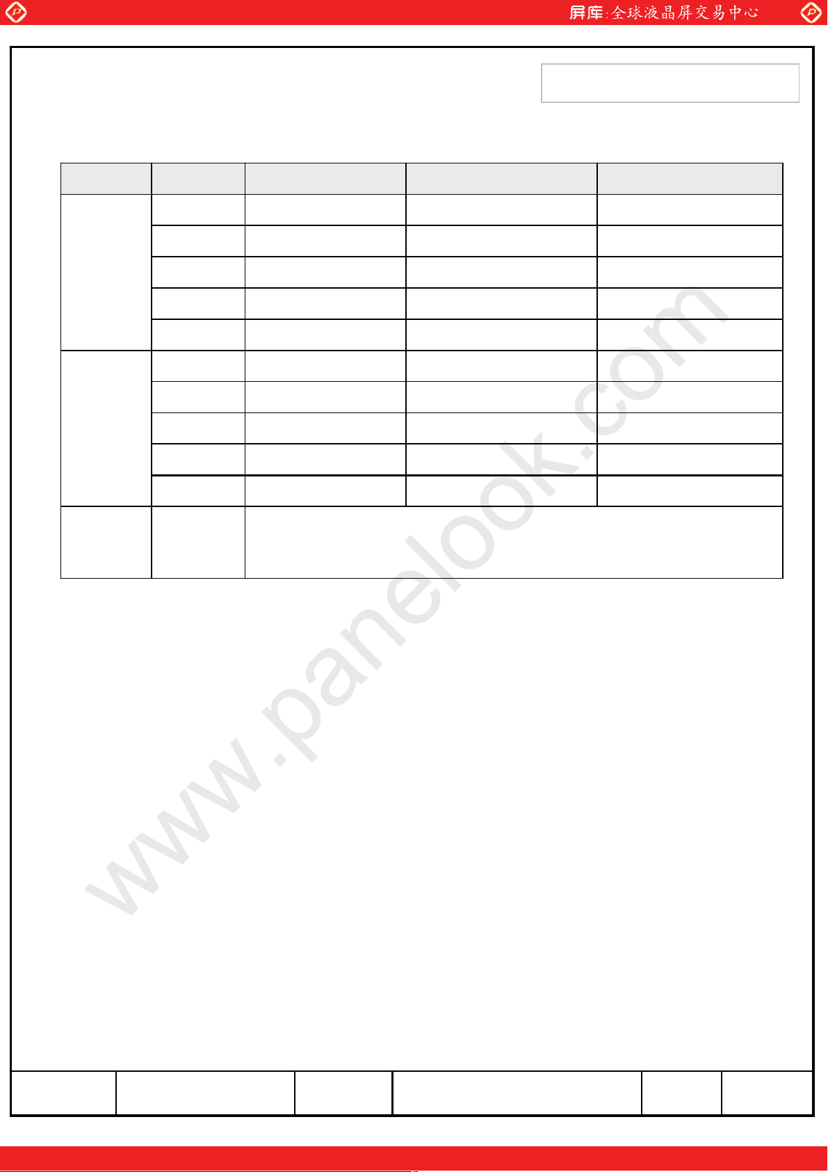
5.3 Back Light Unit
www.panelook.com
Approval Specification
Approval Specification
FunctionColorInputPin No.
High VoltageREDHot11
GroundWhiteCold12
Upper
Lower
-
-
Connect
or
Part No.
High VoltageBlueHot23
GroundGrayCold24
High VoltageREDHot11
GroundWhiteCold12
High VoltageBlueHot23
GroundGrayCold24
YEON-HO 35001HS-04L
One step solution for LCD / PDP / OLED panel application: Datasheet, inventory and accessory!
25/40Page05-000-G-080710Doc. NoLTM230TT01MODEL
www.panelook.com
Page 26
Global LCD Panel Exchange Center
www.panelook.com
Approval Specification
Approval Specification
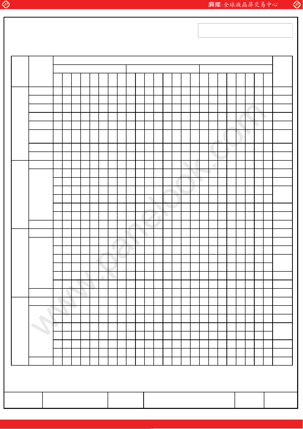
5.3 Input Signals, Basic Display Colors and Gray Scale of Each Color
DATA SIGNAL
COLOR
BASIC
COLOR
GRAY
SCALE
OF
RED
GRAY
SCALE
OF
GREEN
GRAY
SCALE
OF
BLUE
DISPLAY
(8bit)
DARK
˦
˨
LIGHT
DARK
˦
˨
LIGHT
DARK
˦
˨
LIGHT
B3B2B1B0G7G6G5G4G3G2G1G0R7R6R5R4R3R2R1R0
1111111100000000CYAN
1111111111111WHITE
:::::
00000000011111111RED
:::::::::
:::::::::::::
BLUEGREENRED
:::::::::::::
::::::::::::::::::
:::::::::
::::::::::::::::::
000001111111100000000GREEN
:::::
::::::::::::::::::
GRAY
SCALE
LEVEL
B7B6B5B4
-000000000000000000000000BLACK
-111111110000000000000000BLUE
-000000001111111100000000GREEN
-11111111
-000000000000000011111111RED
-111111110000000011111111MAGENTA
-000000001111111111111111YELLOW
-11111111111
R0000000000000000000000000BLACK
R1000000000000000000000001
R2000000000000000000000010
R3~
R252
R253000000000000000011111101
R254000000000000000011111110
R2550000000
G0000000000000000000000000BLACK
G1000000000000000100000000
G2000000000000001000000000
G3~
G252
G253000000001111110100000000
G254000000001111111000000000
G255000
B0000000000000000000000000BLACK
B1000000010000000000000000
B2000000100000000000000000
B3~
B252
B253111111010000000000000000
B254111111100000000000000000
B255111111110000000000000000BLUE
Note (1) Definition of Gray :
Rn : Red Gray, Gn : Green Gray, Bn : Blue Gray (n = Gray level)
Input Signal : 0 = Low level voltage, 1 = High level voltage
One step solution for LCD / PDP / OLED panel application: Datasheet, inventory and accessory!
26/40Page05-000-G-080710Doc. NoLTM230TT01MODEL
www.panelook.com
Page 27
Global LCD Panel Exchange Center
www.panelook.com
6. Interface Timing
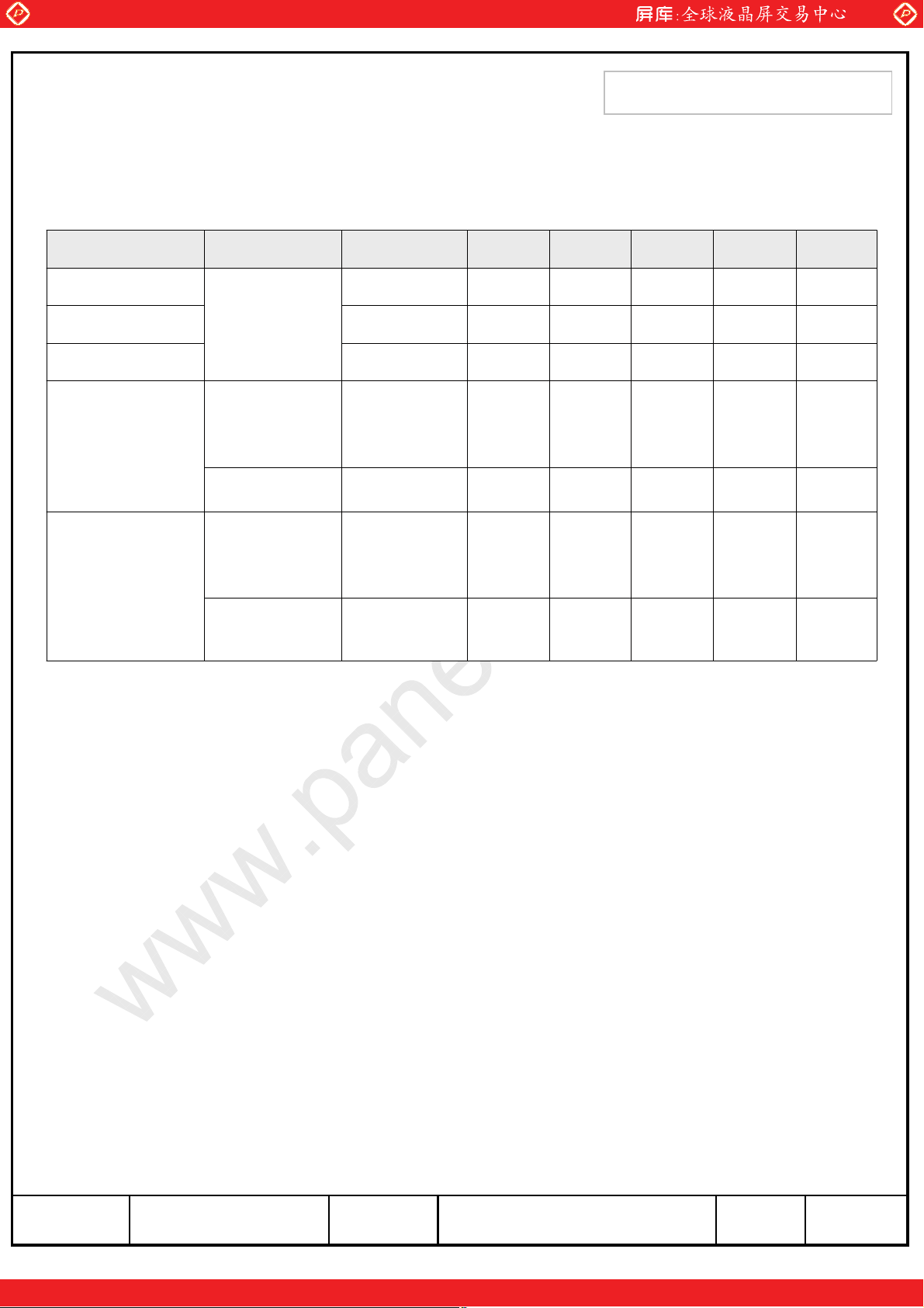
6.1 Timing Parameters ( DE only mode )
Approval Specification
Approval Specification
NOTEUnitMAX.TYP.MIN.SYMBOLITEMSIGNAL
Clock
Hsync
Vsync
Frequency
C
H
V
Active
Vertical
Display Term
Display
Period
Vertical Total
VD
V
Active
Horizontal
Display
Period
HD
clocks102410241024T
Display Term
Horizontal
Total
H
clocks-1104-T
Note (1) This product is DE only mode. The input of Hsync & Vsync signal does
not have an effect on normal operation.
-MHz8278.563.81/T
-KHz73.57157.8F
-Hz626049F
-lines115211521152T
-lines118611851181T
YV
YV
(2) Test Point : TTL control signal and CLK at LVDS Tx input terminal in system
(3) Internal Vcc = 3.3V
(4) Best operation clock frequency is 78.5MHz (60Hz)
(5) Clock frequency = Frame frequency x
(Typ) x
V
T
H
(Typ)
T
(6) Max, Min variation range is at main clock Typ value (78.5MHz).
One step solution for LCD / PDP / OLED panel application: Datasheet, inventory and accessory!
27/40Page05-000-G-080710Doc. NoLTM230TT01MODEL
www.panelook.com
Page 28
Global LCD Panel Exchange Center
www.panelook.com
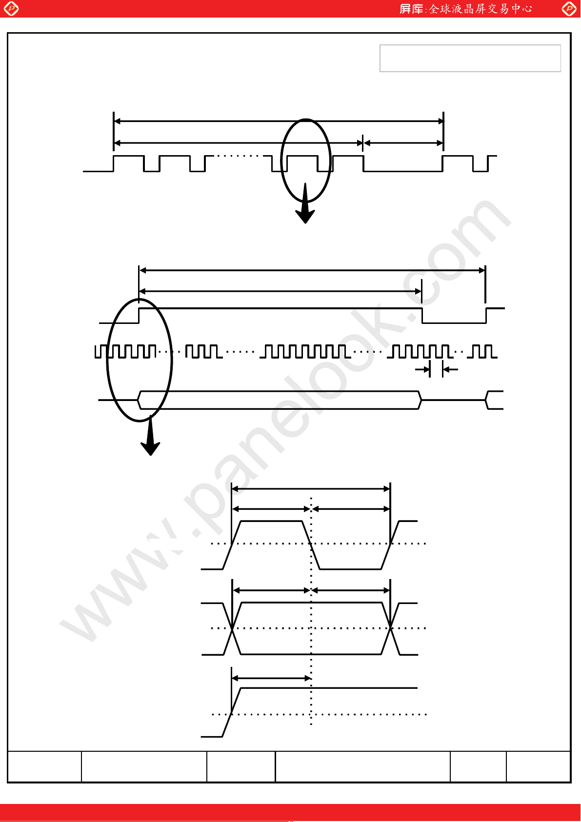
6.2 Timing diagrams of interface signal ( DE only mode )
T
V
T
VD
DE
T
H
T
HD
Approval Specification
Approval Specification
T
VB
DE
D
CLK
DATA
SIGNALS
D
CLK
T
C
T
C
T
CH
T
CL
0.5
V
CC
T
DS
T
DH
DISPLAY
DATA
DE
T
ES
0.5
V
CC
0.5
V
CC
One step solution for LCD / PDP / OLED panel application: Datasheet, inventory and accessory!
28/40Page05-000-G-080710Doc. NoLTM230TT01MODEL
www.panelook.com
Page 29
Global LCD Panel Exchange Center
www.panelook.com
Approval Specification
Approval Specification
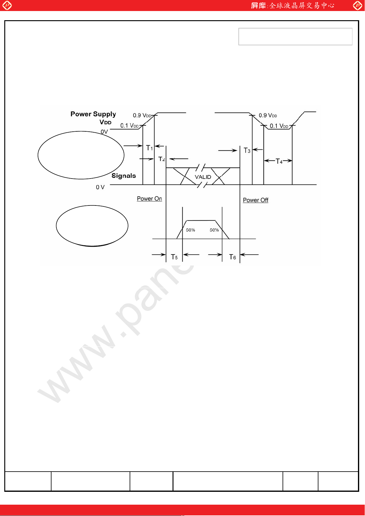
6.3 Power ON/OFF Sequence
To prevent a latch-up or DC operation of the LCD Module, the power on/off
sequence should be as the diagram below.
300༕༕༕༕˺˺˺˺T1˺˺˺˺10msec
0˺˺˺˺T2˺˺˺˺50msec
0˺˺˺˺T3˺˺˺˺50msec
1sec˺˺˺˺T4
Back-Light
(Recommended)
500msec˺˺˺˺T5
100msec˺˺˺˺T6
T1 : VDDrising time from 10% to 90%
T2 : The time from V
T3 : The time from valid data off to V
T4 : V
off time for Windows restart
DD
to valid data at power ON.
DD
off at power Off.
DD
T5 : The time from valid data to B/L enable at power ON.
T6 : The time from valid data off to B/L disable at power Off.
The supply voltage of the external system for the Module input should be the same
as the definition of V
DD
.
Apply the lamp voltage within the LCD operation range. When the back light turns on
before the LCD operation or the LCD turns off before the back light turns off,
the display may momentarily show abnormal screen.
In case of V
= off level,
DD
please keep the level of input signals low or keep a high impedance.
T4 should be measured after the Module has been fully discharged between power off
and on period.
Interface signal should not be kept at high impedance when the power is on.
One step solution for LCD / PDP / OLED panel application: Datasheet, inventory and accessory!
29/40Page05-000-G-080710Doc. NoLTM230TT01MODEL
www.panelook.com
Page 30
Global LCD Panel Exchange Center
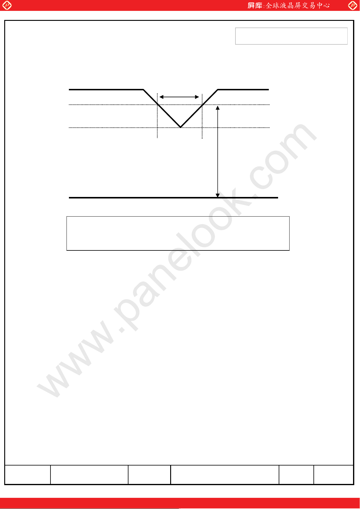
6.4 VDD Power Dip Condition
V
DD
90%
www.panelook.com
T
d
Approval Specification
Approval Specification
80%
V
CC
GND
4.5V ˺ VDD˺ 5.5V
If V
(typ.) x 80% ˺ VCC˺ VDD(typ) x 90%
DD
Then, 0<Td ˺20msec
Note (1) The above conditions are for the glitch of the input voltage.
(2) For stable operation of an LCD Module power, please follow them.
i.e., if typ VDD x 80% ᆙ Vcc ᆙ typ VDD x 90%, then T
should be less than 20ms.
d
One step solution for LCD / PDP / OLED panel application: Datasheet, inventory and accessory!
30/40Page05-000-G-080710Doc. NoLTM230TT01MODEL
www.panelook.com
Page 31
Global LCD Panel Exchange Center
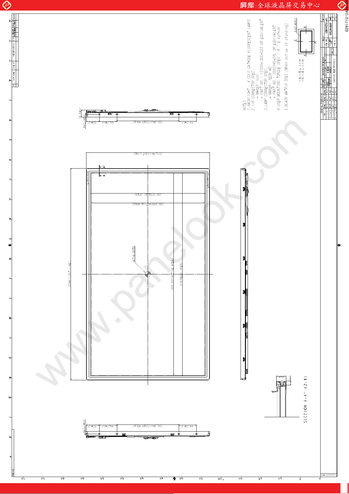
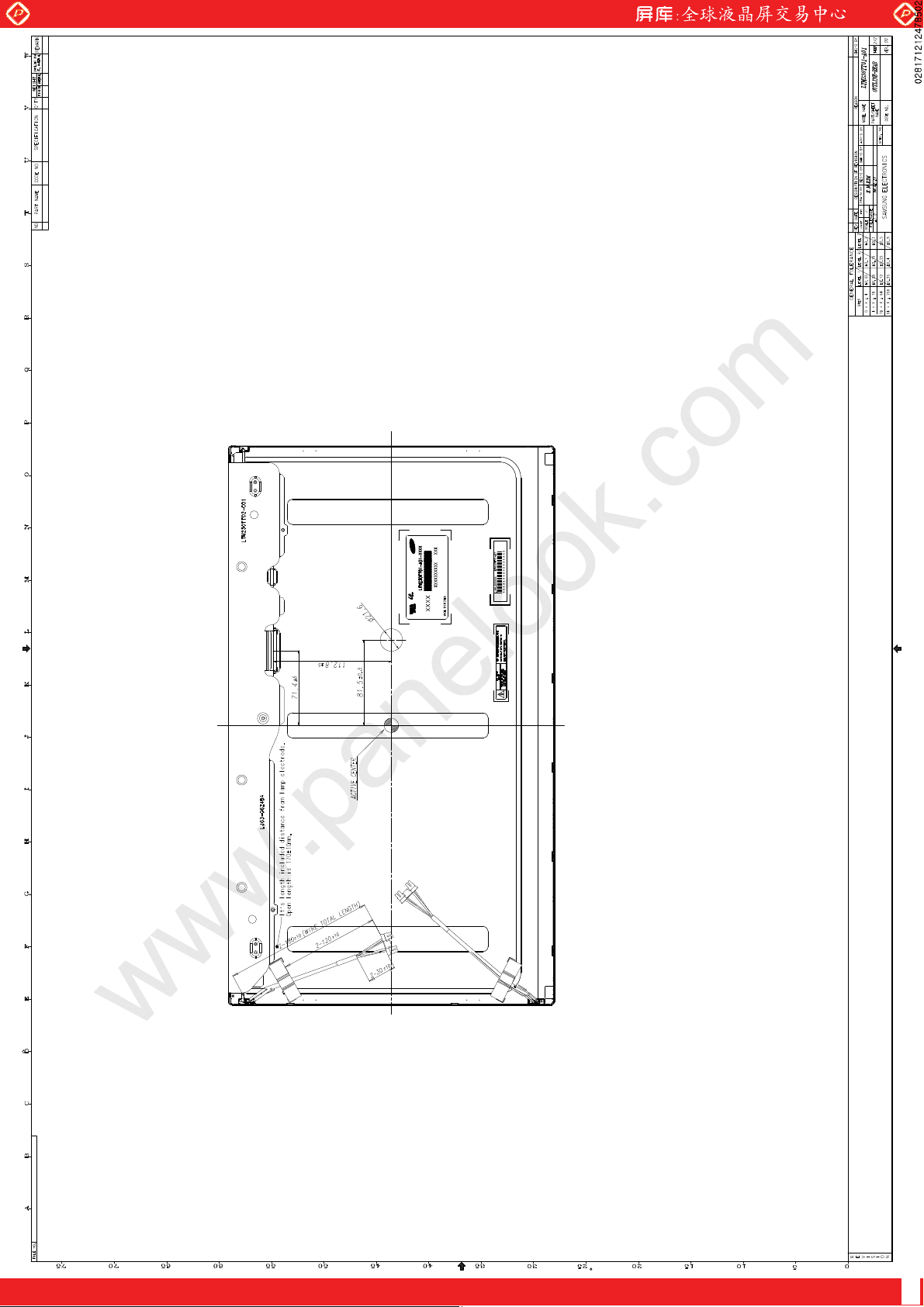
7. Outline Dimension
[ Refer to the next page ]
www.panelook.com
Approval Specification
Approval Specification
One step solution for LCD / PDP / OLED panel application: Datasheet, inventory and accessory!
31/40Page05-000-G-080710Doc. NoLTM230TT01MODEL
www.panelook.com
Page 32
Global LCD Panel Exchange Center
www.panelook.com
One step solution for LCD / PDP / OLED panel application: Datasheet, inventory and accessory!
www.panelook.com
Page 33
Global LCD Panel Exchange Center
www.panelook.com
One step solution for LCD / PDP / OLED panel application: Datasheet, inventory and accessory!
www.panelook.com
Page 34
Global LCD Panel Exchange Center
8. Reliability Test
www.panelook.com
Approval Specification
Approval Specification
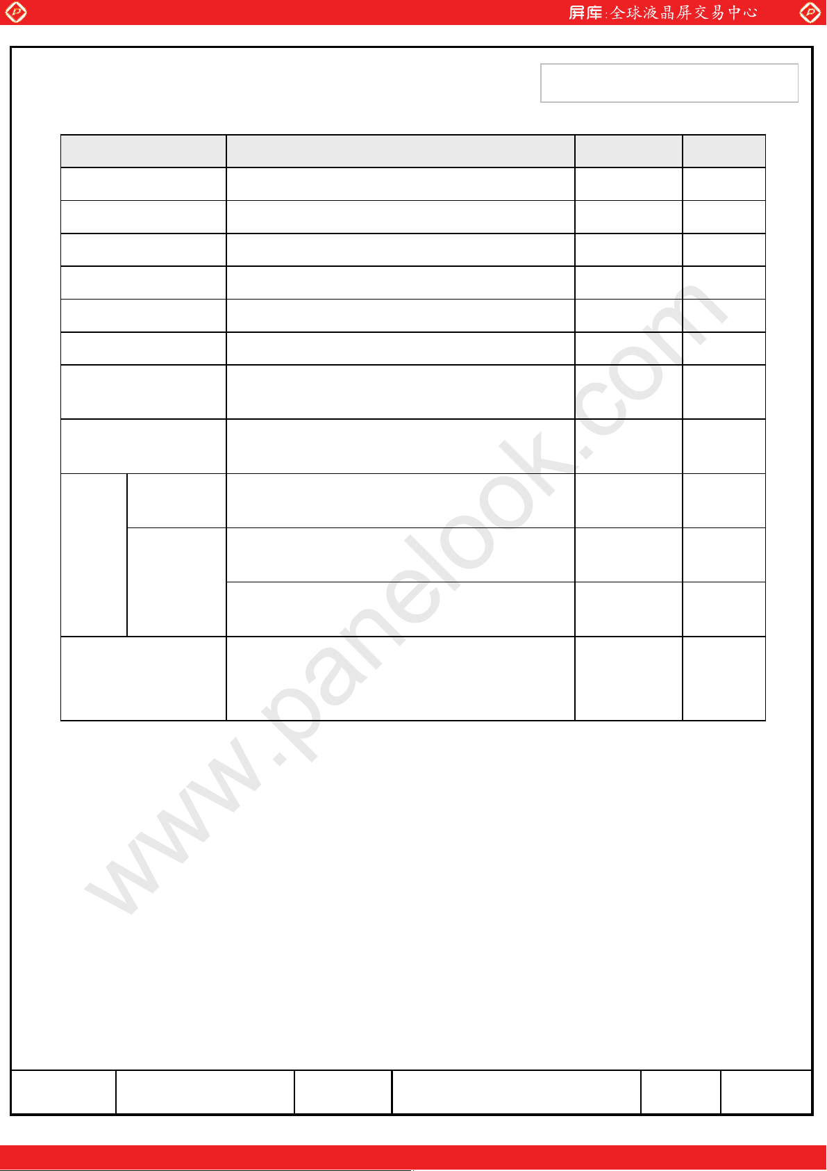
SampleTime/CycleConditionsTest Items
12500 hrs50¶C , BiasHTOL*
8250 hrs0¶C , BiasLTOL*
4500 hrs40¶C / 95% , BiasTHB**
4500 hrs70¶C , No BiasHTS***
4500 hrs-20¶C , No BiasLTS***
8200 cycle-20¶C/30min ~ +60¶C/30min , No biasThermal Cycle
Shock
(Non-operating)
Vibration
(Non-operating)
Non-
Operating
ESD 3· 8kV
Operating
Altitude
50G , 11msec
Sine wave , · x/y/z axis
1.5G , 5~200 Hz
x/y/z axis , sweep rate : 10 min
Contact : 150pF, 330˟˟˟˟, 100point,
once/point
Air(non-contact) : 150pF, 330˟˟˟˟, 100point,
once/point
Thermal :-10~50ଇ, 15000ft(Operating),
40000ft(Non-operating)
Normal :45ଇ, 15000ft
8Hr
10Hr
[ Result Evaluation Criteria]
Under the display quality test conditions with normal operation state, these should
be no change which may affect practical display functions.
31 time/axis
330min/axis
3· 10kVCDM : 150pF, 330˟˟˟˟, 9point, 3 times/point
3· 15kV
3
3
* HTOL/ LTOL : High/Low Temperature Operating Life
** THB : Temperature Humidity Bias
*** HTS/LTS : High/Low Temperature Storage
One step solution for LCD / PDP / OLED panel application: Datasheet, inventory and accessory!
34/40Page05-000-G-080710Doc. NoLTM230TT01MODEL
www.panelook.com
Page 35
Global LCD Panel Exchange Center
9. PACKING
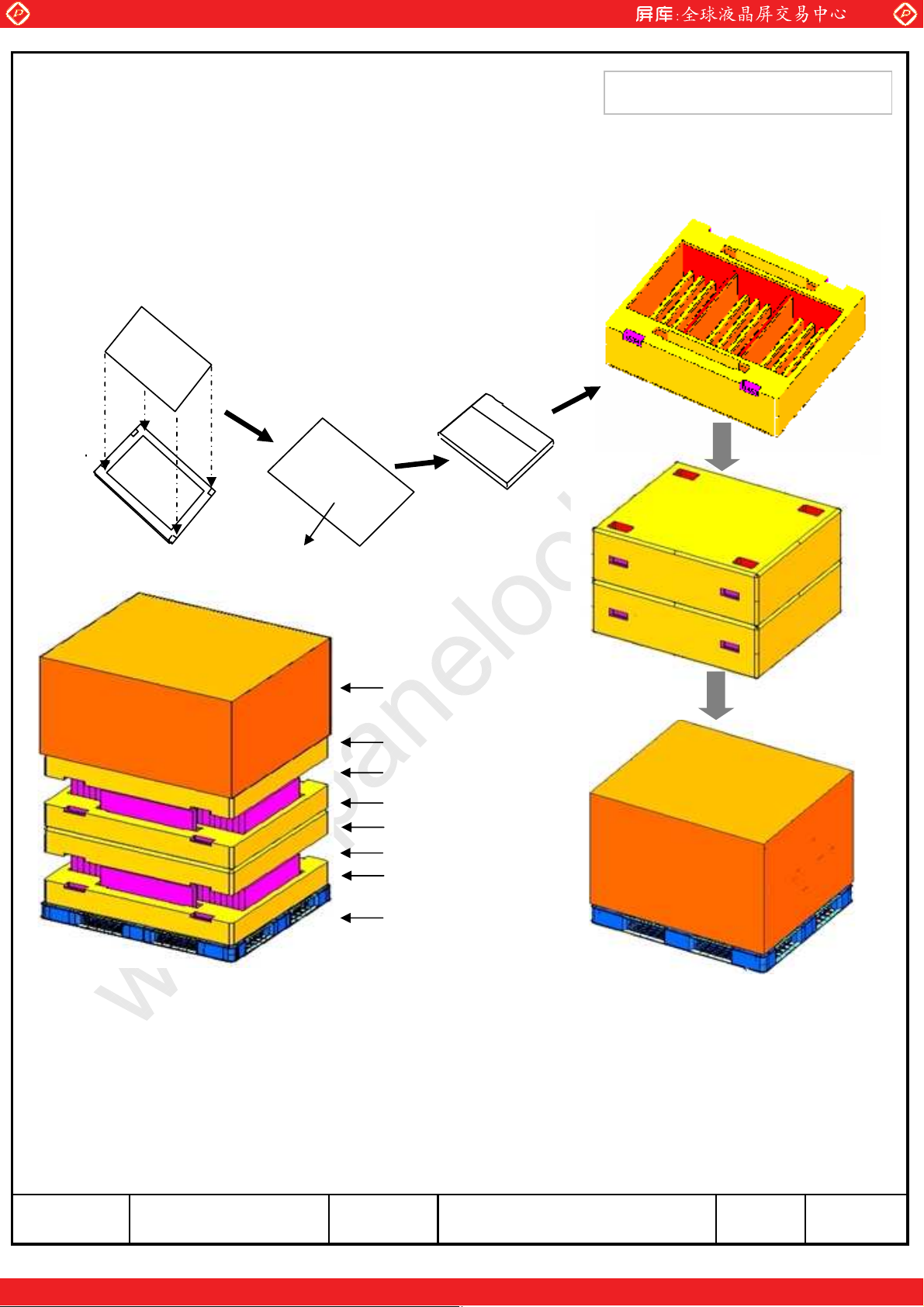
9.1 CARTON
(1) Packing Form
www.panelook.com
Approval Specification
Approval Specification
EPS-Cushion Pad
(2) Packing Method
a. Without Inverter
Panel Protector
Panel
EPS Cushion
Shielding-Bag
NOTE 1)
2) Cushion Material : EPS
3) Cushion Size : 1,120(W) x 955(D) x 216(H)
4) Packing Pallet Box Material : DW4
Packing Pallet Box
Cushion Cover
Module (17PCS)
Cushion Cover
Cushion Cover
Module (17PCS)
Cushion Cover
Pallet Plastic
TOTAL : Approx. 102.0Kg · 5%
5) Packing Pallet Box Size : 1,145(W) x 980(D) x 875(H)
One step solution for LCD / PDP / OLED panel application: Datasheet, inventory and accessory!
35/40Page05-000-G-080710Doc. NoLTM230TT01MODEL
www.panelook.com
Page 36
Global LCD Panel Exchange Center
(2) Packing Specification
LCD
Packing
Packing-Pallet Box
www.panelook.com
Approval Specification
Approval Specification
RemarkSpecificationITEM
1. Panel : 34 PCS
( 17 PCS x 2 Stair = 34 PCS )
2. Cushion Cover : 4 EA
3. Packing Pallet Box : 1 EA
1Box/PalletPallet
Packing
Direction
1. Pallet Plastic : 1ea
2. Pallet Plastic Size : W1150 x L985 x H125
-Vertical
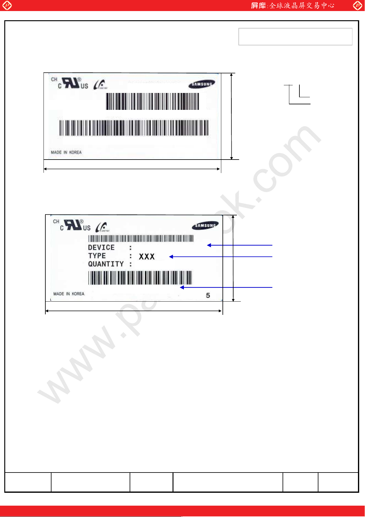
10. MARKING & OTHERS
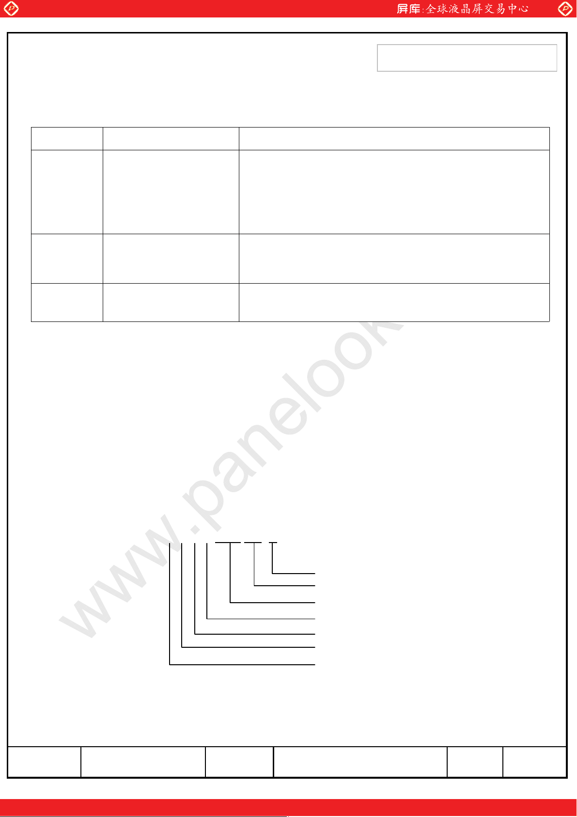
A nameplate bearing followed by is affixed to a shipped product at the specified
location on each product.
(1) Parts number : LTM230TT01
(2) Revision: Three letters
(3) Lot number : X X X X XXX
XX X
Cell Position No. (In the Glass)
Glass No. (In the one Lot)
Lot No. (Glass)
Month
Year
Product code
Line
One step solution for LCD / PDP / OLED panel application: Datasheet, inventory and accessory!
36/40Page05-000-G-080710Doc. NoLTM230TT01MODEL
www.panelook.com
Page 37
Global LCD Panel Exchange Center
(4) Nameplate Indication
[Week Code]
80mm
www.panelook.com
LTM230TT01
[Lot Number] [Revision]
PPID
Approval Specification
Approval Specification
Week code : 08 12
40mm
week
year
(5) Packing box attach
40mm
LTM230TT01
XXXPCS
XXXXXXXXXX
80mm
(6) Others
a. After service part
Lamps cannot be replaced because of the narrow bezel structure.
Part number
Revision code
Box serial number
One step solution for LCD / PDP / OLED panel application: Datasheet, inventory and accessory!
37/40Page05-000-G-080710Doc. NoLTM230TT01MODEL
www.panelook.com
Page 38
Global LCD Panel Exchange Center
11. General Precautions
www.panelook.com
Approval Specification
Approval Specification
11.1 Handling
(a) When the module is assembled, it should be attached to the system firmly
using all mounting holes. Be careful not to twist and bend the module.
(b) Because the inverter uses high voltages, it should be disconnected from power
source before it is assembled or disassembled.
(c) Refrain from strong mechanical shock and / or any force to the module.
In addition to damage, it may cause improper operation or damage to the module
and CCFT back light.
(d) Note that polarizer films are very fragile and could be damaged easily.
Do not press or scratch the surface harder than a HB pencil lead.
(e) Wipe off water droplets or oil immediately. If you leave the droplets for a long
time, staining or discoloration may occur.
(f) If the surface of the polarizer is dirty, clean it using absorbent cotton or soft cloth.
(g) Desirable cleaners are water, IPA (Isopropyl Alcohol) or Hexane.
Do not use Ketone type materials (ex. Acetone), Ethyl alcohol, Toluene, Ethyl acid
or Methyl chloride. It might cause permanent damage to the polarizer due to chemical
reaction.
(h) If the liquid crystal material leaks from the panel, it should be kept away
from the eyes or mouth . In case of contact with hands, legs or clothes, it must
be washed away with soap thoroughly.
(i) Protect the Module from static, or the CMOS Gate Array IC would be damaged.
(j) Use finger-stalls with soft gloves in order to keep display clean during the
incoming inspection and assembly process.
(k) Do not disassemble the Module.
(l) Do not pull or fold the lamp wire.
(m) Do not adjust the variable resistor located on the Module.
(n) Protection film for polarizer on the Module should be slowly peeled off just before use
so that the electrostatic charge can be minimized.
(o) Pins of I/F connector should not be touched directly with bare hands.
One step solution for LCD / PDP / OLED panel application: Datasheet, inventory and accessory!
38/40Page05-000-G-080710Doc. NoLTM230TT01MODEL
www.panelook.com
Page 39
Global LCD Panel Exchange Center
www.panelook.com
Approval Specification
Approval Specification
11.2 Storage
(a) Do not leave the Module in high temperature, and high humidity for a long time.
It is highly recommended to store the Module with temperature from 0 to 35
and relative humidity of less than 70%.
(b) Do not store the TFT-LCD Module in direct sunlight.
(c) The Module should be stored in a dark place. It is prohibited to apply sunlight or
fluorescent light in storing.
11.3 Operation
(a) Do not connect or disconnect the Module in the "Power On" condition.
(b) Power supply should always be turned on/off by the item 6.3
"Power on/off sequence"
(c) Module has high frequency circuits. Sufficient suppression to the electromagnetic
interference should be done by system manufacturers. Grounding and shielding
methods may be important to minimize the interference.
(d) The cable between the back light connector and its inverter power supply should
be connected directly with a minimized length. A longer cable between
the back light and the inverter may cause lower luminance of lamp(CCFT) and
may require higher startup voltage(Vs).
11.4 Operation Condition Guide
(a) The LCD product should be operated under normal conditions.
Normal condition is defined as below;
- Temperature : 20·15
- Humidity : 65·20%
- Display pattern : continually changing pattern (Not stationary)
(b) If the product will be used in extreme conditions such as high temperature,
humidity, display patterns or operation time etc.., It is strongly recommended
to contact SEC for Application engineering advice. Otherwise, its reliability and
function may not be guaranteed. Extreme conditions are commonly found at
Airports, Transit Stations, Banks, Stock market, and Controlling systems.
One step solution for LCD / PDP / OLED panel application: Datasheet, inventory and accessory!
39/40Page05-000-G-080710Doc. NoLTM230TT01MODEL
www.panelook.com
Page 40
Global LCD Panel Exchange Center
www.panelook.com
Approval Specification
Approval Specification
11.5 Others
(a) Ultra-violet ray filter is necessary for outdoor operation.
(b) Avoid condensation of water. It may result in improper operation or disconnection
of electrode.
(c) Do not exceed the absolute maximum rating value. ( supply voltage variation,
input voltage variation, variation in part contents and environmental temperature,
and so on)
Otherwise the Module may be damaged.
(d) If the Module keeps displaying the same pattern for a long period of time,
the image may be "sticked" to the screen.
To avoid image sticking, it is recommended to use a screen saver.
(e) This Module has its circuitry PCB's on the rear side and should be handled
carefully in order not to be stressed.
(f) Please contact SEC in advance when you display the same pattern for a long time.
One step solution for LCD / PDP / OLED panel application: Datasheet, inventory and accessory!
40/40Page05-000-G-080710Doc. NoLTM230TT01MODEL
www.panelook.com
 Loading...