

Page 1
Global LCD Panel Exchange Center
ISSUED DATE : 2011-05-31
SAMSUNG TFT-LCD PRODUCT INFORMATION
MODEL : LTM215HT04-V
www.panelook.com
PRODUCT INFORMATION
Note : This is Product Information is subject to change after 3 months of issuing date.
Application Engineering Group
LCD Business, Samsung Electronics Co . , LTD.
MODEL LTM215HT04 Page
One step solution for LCD / PDP / OLED panel application: Datasheet, inventory and accessory!
1/33
www.panelook.com
Page 2
Global LCD Panel Exchange Center
Contents
General Description --------------------------------------------------------------------------------- (3)
1. Absolute Maximum Ratings ------------------------------------------------------------------- (4)
2. Optical Characteristics -------------------------------------------------------------------------- (6)
3. Electrical Characteristics ------------------------------------------------------------------------(11)
3.1 TFT LCD Module
3.2 Back Light Unit
4. Block Diagram ----------------------------------------------------------------------------------- (15)
4.1 TFT LCD Module
4.2 Back Light Unit
www.panelook.com
PRODUCT INFORMATION
5. Input Terminal Pin Assignment -------------------------------------------------------------- (16)
5.1 Input Signal & Power
5.2 LVDS Interface
5.3 Back Light Unit
5.4 Input Signals, Basic Display Colors and Gray Scale of Each Color
6. Interface Timing --------------------------------------------------------------------------------- (25)
6.1 Timing Parameters (DE only mode)
6.2 Timing Diagrams of interface Signal (DE only mode)
6.3 Power ON/OFF Sequence
6.4 VDD Power Dip Condition
7. Outline Dimension ------------------------------------------------------------------------------- (29)
8. General Precaution ------------------------------------------------------------------------------ (31)
8.1 Handling
8.2 Storage
8.3 Operation
8.4 Operation Condition Guide
8.5 Others
MODEL LTM215HT04 Page
One step solution for LCD / PDP / OLED panel application: Datasheet, inventory and accessory!
2/33
www.panelook.com
Page 3
Global LCD Panel Exchange Center
www.panelook.com
General Description
PRODUCT INFORMATION
Description
LTM215HT04 is a color active matrix liquid crystal display (LCD) that uses amorphous
silicon TFT (Thin Film Transistor) as switching components. This model is composed of
a TFT LCD panel, a driver circuit and a back light unit. The resolution of a 21.5” is 1920
x 1080 and this model can display up to 16.7 millions colors.
Features
High contrast ratio, high aperture structure
High speed response
FHD (1920 x 1080 pixels) resolution
Low power consumption
LVDS interface (2pixel/clock), DE(Data Enable) Mode
White LED Edge slim Backlight (1-side bar)
RoHS compliance, Halogen Free
TCO5.2 compliance
( Except for 2.2 response time; this product does not have over driving function.
It is recommended to support in system level )
Applications
Workstation & desktop monitors
Display terminals for AV application products
Monitor for HDTV
* If the module is used to other applications besides the above, please contact SEC
in advance.
General Information
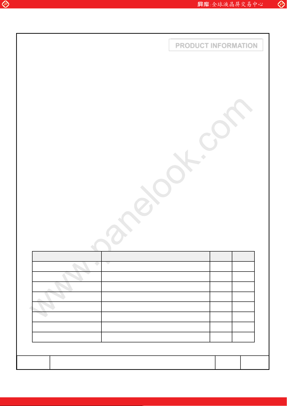
Items Specification Unit Note
Pixel Pitch 248.25(H) x 248.25(W) um
Active Display Area 476.64(H) x 268.11(V) mm
Surface Treatment Haze 25%, Hard –coating(3H)
Display Colors 16.7M ( 6bit + Hi-FRC ) colors
Number of Pixels 1920 X 1080 pixel
Pixel Arrangement RGB vertical stripe
Display Mode Normally White
Luminance of White 250(Typ.)
cd/༇
MODEL LTM215HT04 Page
One step solution for LCD / PDP / OLED panel application: Datasheet, inventory and accessory!
3/33
www.panelook.com
Page 4
Global LCD Panel Exchange Center
Mechanical Information
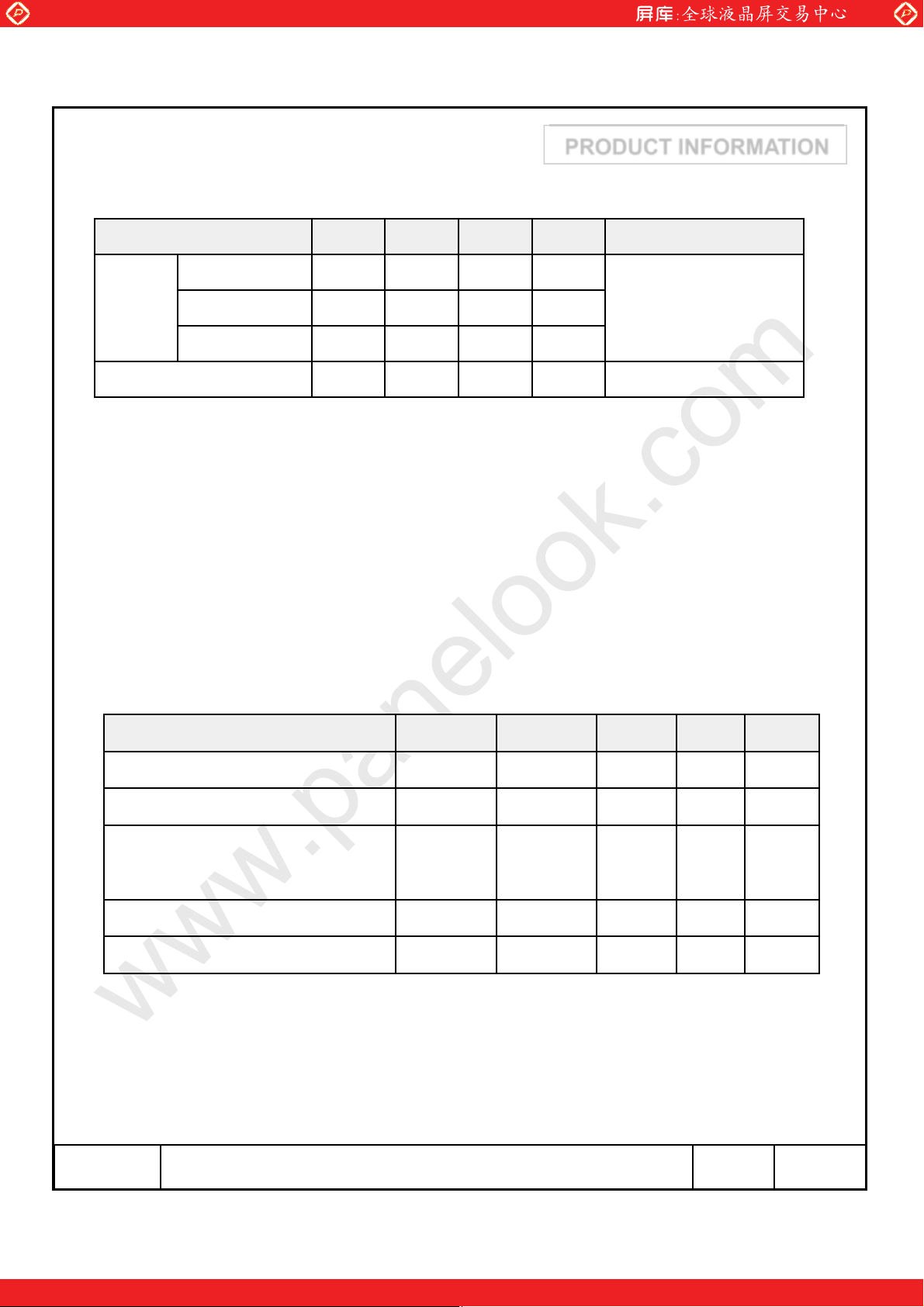
Item Min. Typ. Max. Unit Note
Horizontal (H) 495.1 495.6 496.1 mm
Module
size
Depth (D) 10.7 mm
Weight - - 1,980 g LCD module only
www.panelook.com
PRODUCT INFORMATION
-Vertical (V) 291.7 292.2 292.7 mm
Note (1) Mechanical tolerance is · 0.5mm unless there is a special comment.
1. Absolute Maximum Ratings
If the condition exceeds maximum ratings, it can cause malfunction or unrecoverable
damage to the device.
Item Symbol Min. Max. Unit Note
Power Supply Voltage V
Storage temperature T
Glass surface temperature
(Operation condition)
T
DD
STG
OPR
GND-0.5 5.5 V
-20 60
050
(1)
Shock ( non - operating ) S
Vibration ( non - operating ) V
nop
nop
-50G(2)
- 1.5 G (3)
Note (1) Ta= 25 · 2 ¶C
MODEL LTM215HT04 Page
One step solution for LCD / PDP / OLED panel application: Datasheet, inventory and accessory!
4/33
www.panelook.com
Page 5
Global LCD Panel Exchange Center
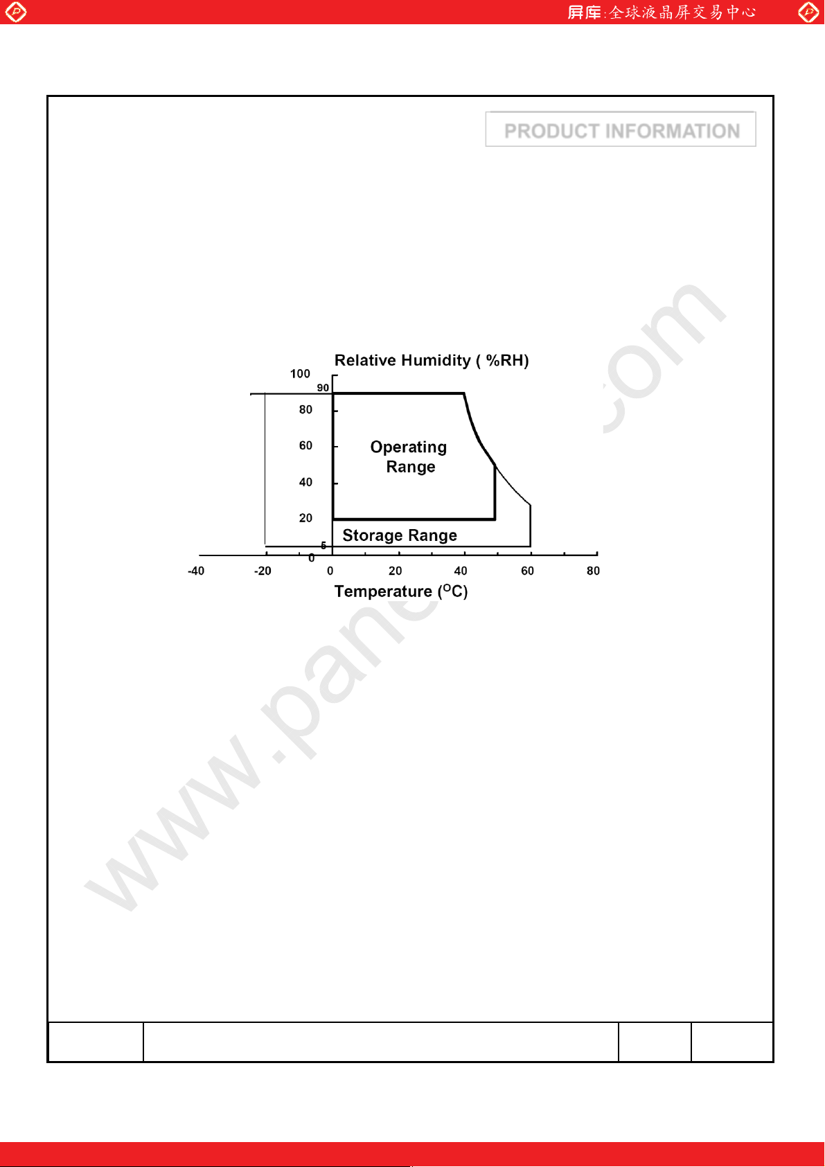
(1) Temperature and relative humidity range are shown in the figure below.
a. 90 % RH Max. (Ta ≤ 39 ¶C)
b. Maximum wet-bulb temperature at 39 ¶C or less. (Ta ≤ 39 ¶C)
c. No condensation
(2) 11ms, sine wave, one time for ·X, ·Y, ·Z axis
(3) 10-300 Hz, Sweep rate 10min, 30min for X,Y,Z axis
www.panelook.com
(39,90)
(39,90)
(39,90)
(39,90)
PRODUCT INFORMATION
25,5)
25,5)
((--25,5)
((--25,5)
Fig. Temperature and Relative humidity range
(50,50.4)
(50,50.4)
(50,50.4)
(50,50.4)
(60,27.7)
(60,27.7)
(60,27.7)
(60,27.7)
MODEL LTM215HT04 Page
One step solution for LCD / PDP / OLED panel application: Datasheet, inventory and accessory!
5/33
www.panelook.com
Page 6
Global LCD Panel Exchange Center
www.panelook.com
2. Optical Characteristics
PRODUCT INFORMATION
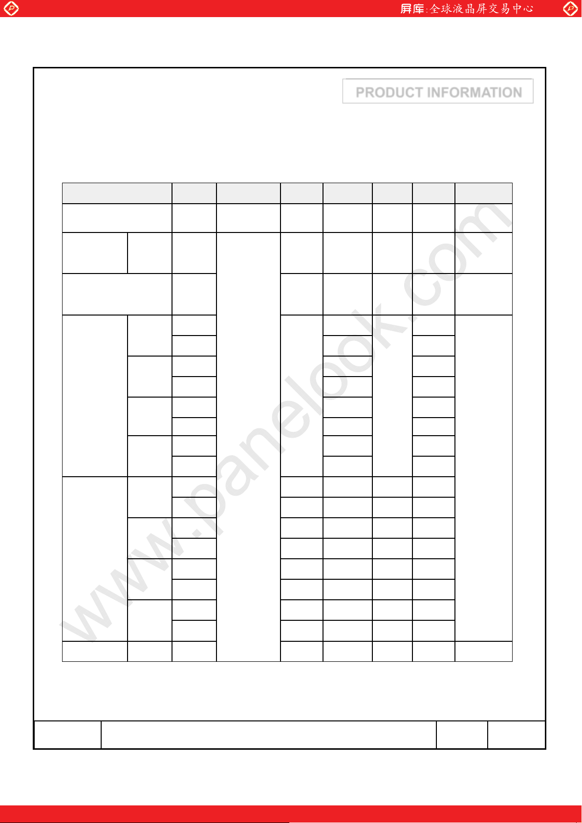
The optical characteristics should be measured in a dark room or equivalent.
Measuring equipment : SR-3, RD-80S (TOPCON), EZ-Contrast (Eldim)
(Ta = 25 · 2¶C, VDD=5V, fv= 60Hz, fDCLK= 67.3MHz, If = 330 mA)
Item Symbol Condition Min. Typ. Max. Unit Note
Contrast Ratio
(Center of screen)
Response
Time
Luminance of White
(Center of screen)
Color
Chromaticity
(CIE 1931)
On/Off Tr+Tf - 5 10 msec
Green
Blue
Red
C/R 600 1,000 -
Y
L
Rx
Ry 0.340
Gx
Gy 0.622
Bx 0.155
By 0.042
Normal
=0
θ
L,R
=0
θ
U,D
Viewing
Angle
200 250 - cd/m2
0.633
0.320
-0.030
+0.030
(3)
SR-3
(5)
RD-80S
(6)
SR-3
Wx 0.313
White
Wy 0.329 (7),(8)
Ru' - 0.436 - SR-3
Red
Rv' - 0.526 -
Gu' - 0.130 -
Color
Chromaticity
(CIE 1976)
C.G.L White
* C.G.L : Color Grayscale Linearity (continue to the next page)
Green
Blue
White
Gv' - 0.570 -
Bu' - 0.194 -
Bv' - 0.118 -
Wu' - 0.198 -
Wv' - 0.468 -
Ƹu'v'
- - 0.02 (9)
MODEL LTM215HT04 Page
One step solution for LCD / PDP / OLED panel application: Datasheet, inventory and accessory!
6/33
www.panelook.com
Page 7
Global LCD Panel Exchange Center
Item Symbol Condition Min. Typ. Max. Unit Note
Color Gamut - - 72 - %
Color Temperature - - 6500 - K
www.panelook.com
PRODUCT INFORMATION
θ
Hor.
Viewing
Angle
Ver.
Brightness Uniformity
(9 Points)
L
θ
R
θ
U
θ
D
B
uni
CR≥10
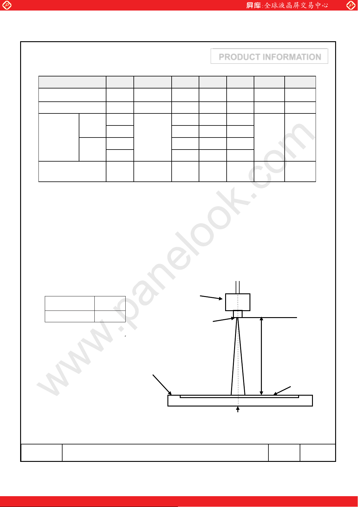
Note (1) Test Equipment Setup
The measurement should be executed in a stable, windless and dark room between
30min after lighting the back light at the given temperature for stabilization
of the back light. This should be measured in the center of screen.
LED current : If = 330mA
Environment condition : Ta = 25 · 2 ¶C
70 80 -
70 80 -
Degrees
70 80 -
70 80 -
--25%
(8)
SR-3
(4)
SR-3
Photo detector
Photo detector Field
SR-3
2ദ
Field
SR-3 : 50
TFT - LCD Module
LCD Panel
The center of the screen
MODEL LTM215HT04 Page
7/33
One step solution for LCD / PDP / OLED panel application: Datasheet, inventory and accessory!
www.panelook.com
Page 8
Global LCD Panel Exchange Center
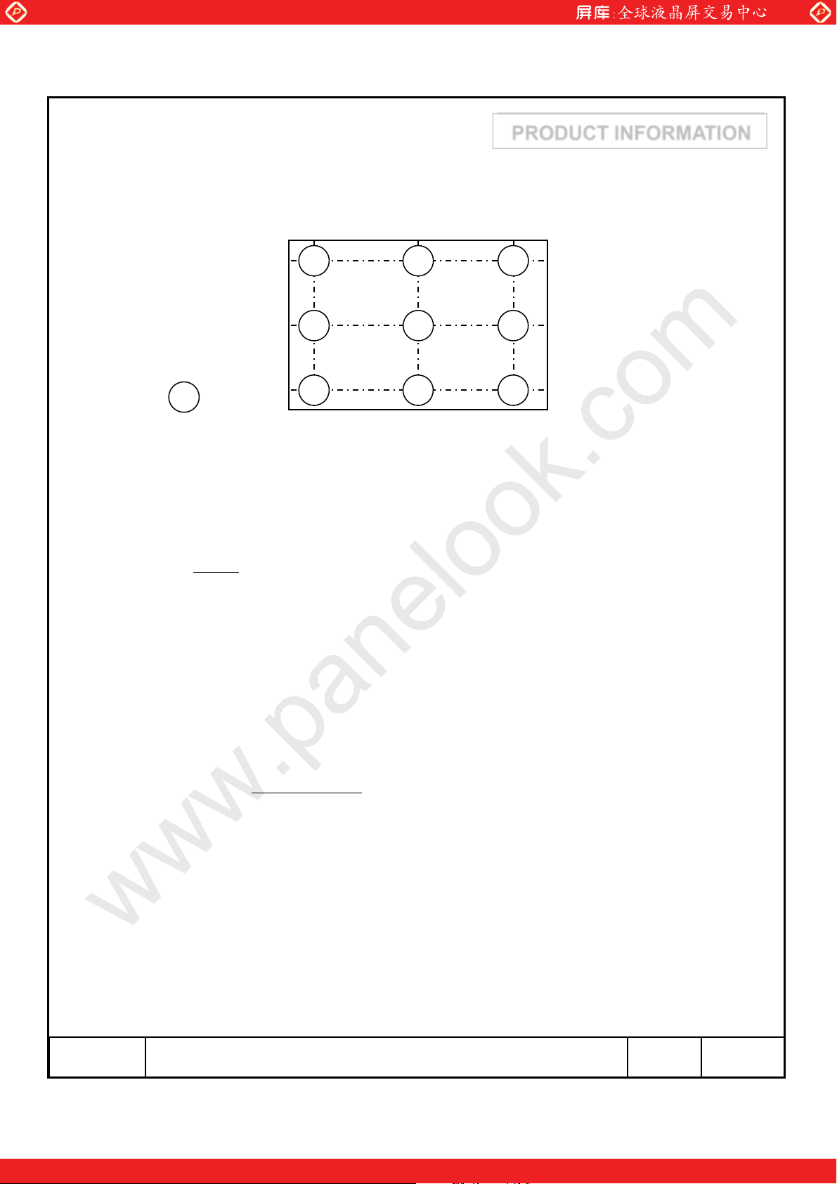
Note (2) Definition of test point
www.panelook.com
PRODUCT INFORMATION
192 960 1728
Active Area
6
: Test Point
Note (3) Definition of Contrast Ratio (C/R)
: Ratio of gray max (Gmax) & gray min (Gmin) at the center point䐣 of the panel
G
CR
max
G
min
Gmax : Luminance with all pixels white
Gmin : Luminance with all pixels black
3 2 1
8 79
45
108
540
972
Note (4) Definition of 9 points brightness uniformity
BB
Buni
Bmax : Maximum brightness with all pixels white
Bmin : Minimum brightness with all pixels white
(max min)
100
B
max
MODEL LTM215HT04 Page
8/33
One step solution for LCD / PDP / OLED panel application: Datasheet, inventory and accessory!
www.panelook.com
Page 9
Global LCD Panel Exchange Center
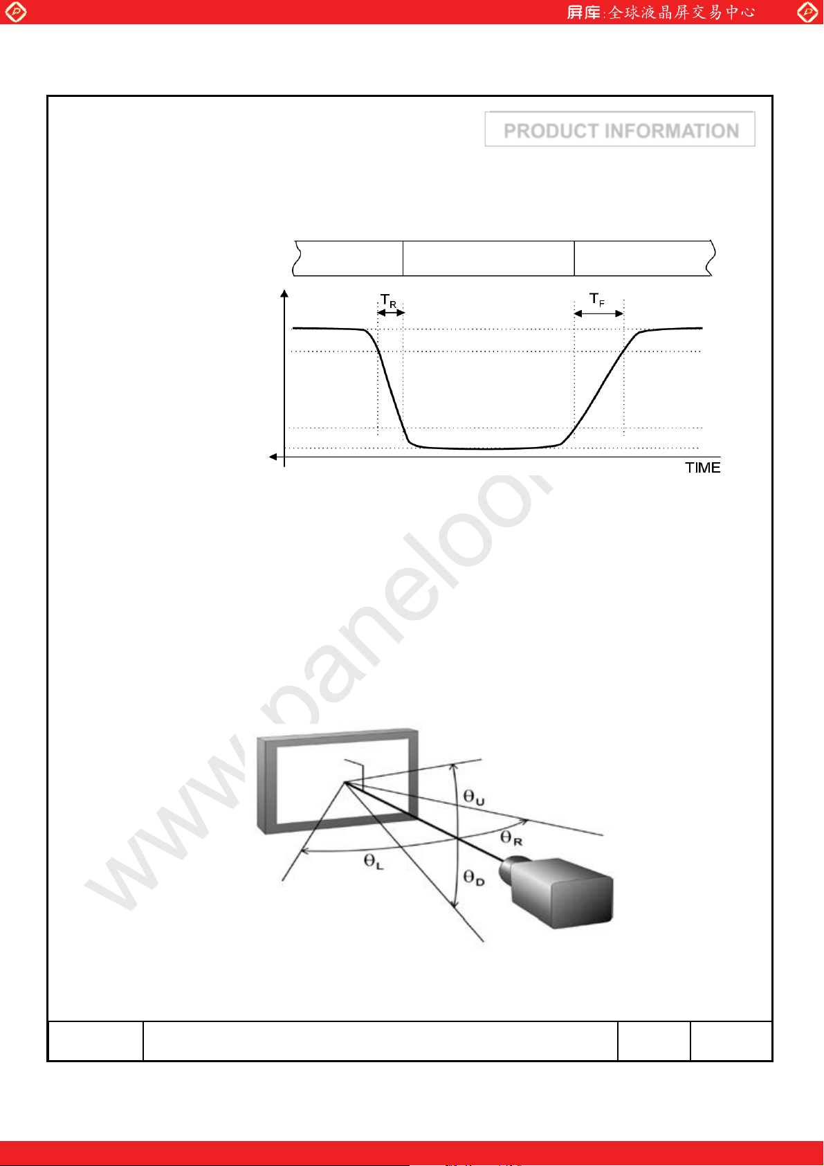
Note (5) Definition of Response time
a. On/Off response time : Sum of Tr, Tf
Display Data White(TFT off) Black(TFT on) White(TFT off)
www.panelook.com
PRODUCT INFORMATION
Optical Instruments
Response
Note (6) Definition of Luminance of White : Luminance of white at center point䐣
Note (7) Definition of Color Chromaticity (CIE 1931, CIE1976)
Color coordinate of Red, Green, Blue & White at center point䐣
Note (8) Definition of Viewing Angle
: Viewing angle range ( CR ≥10 )
100%
90%
10%
0%
MODEL LTM215HT04 Page
One step solution for LCD / PDP / OLED panel application: Datasheet, inventory and accessory!
9/33
www.panelook.com
Page 10
Global LCD Panel Exchange Center
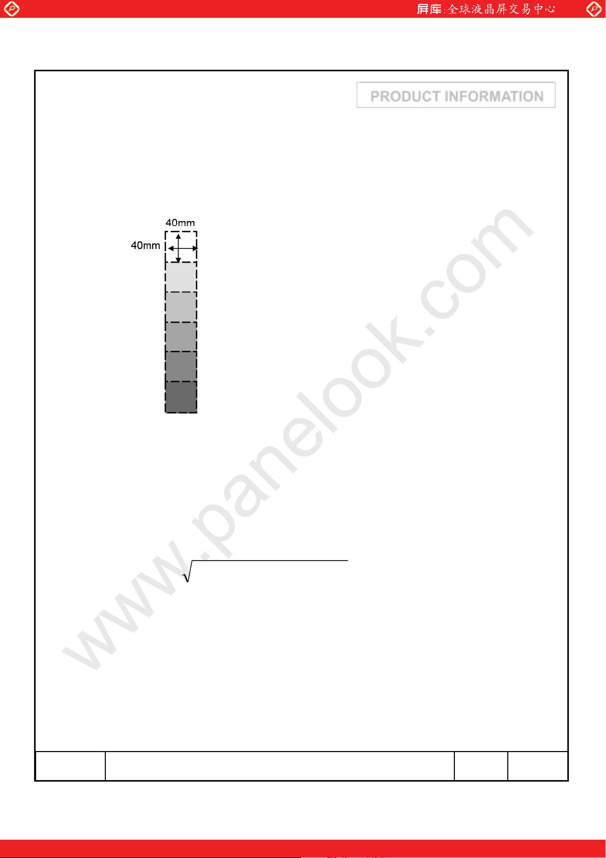
Note (9) Color Grayscale Linearity
a. Test image : 100% full white pattern with a test pattern as below
b. Test pattern : Squares, 40mm by 40mm in size, filled with 255, 225, 195, 165, 135 and
105 grays steps should be arranged at the centerྜྷ of the screen.
www.panelook.com
PRODUCT INFORMATION
c. Test method
st
gray step : move a square of 255 gray level should be moved into the center of the
-1
screen and measure luminance and u’ and v’ coordinates.
- Next gray step : Move a 225 gray square into the center and measure both
luminance and coordinates, too.
d. Test evaluation
u'v'= (u' - u' ) + (v' - v' )
Where A, B : 2 gray levels found to have the largest color differences between them
i.e. get the largest Δu’ and Δv’ of each 6 pair of u’ and v’ and calculate the Δu’v’.
AB
2
AB
2
MODEL LTM215HT04 Page
One step solution for LCD / PDP / OLED panel application: Datasheet, inventory and accessory!
10/33
www.panelook.com
Page 11
Global LCD Panel Exchange Center
www.panelook.com
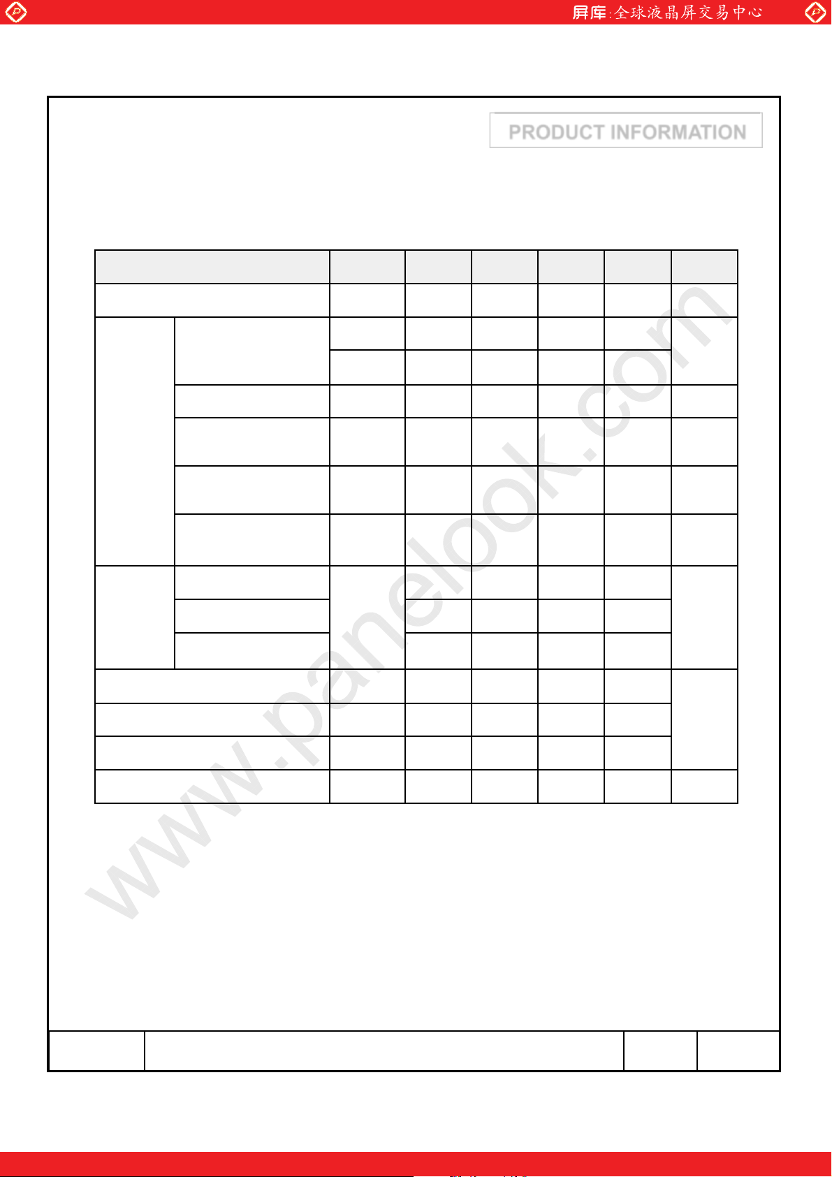
3. Electrical Characteristics
3.1 TFT LCD Module
The connector for display data & timing signal should be connected.
Item Symbol Min. Typ. Max. Unit Note
Voltage of Power Supply V
Differential Input
Voltage for LVDS
Receiver Threshold
LVDS
Input
Characteri
stics
LVDS skew t
Differential input
voltage
Input voltage range
(single-ended)
Common mode
voltage
PRODUCT INFORMATION
DD
High - - +100 mV
Low -100 - - mV
SKEW
| 200 - 600 mV (4)
|V
ID
V
IN
V
CM
4.5 5.0 5.5 V (1)
-300 - 300 ps (3)
0 - 2.4 V (4)
|V
0+
ID
|/2
1.2
2.4-
|V
|/2
ID
V(4)
Ta = 2 5 ¶C
(2)
(a) Black
- 1000 - mA
Current of
Power
(b) White - 800 - mA
I
DD
Supply
(c) Dot - 1300 1600 mA
Vsync Frequency f
Hsync Frequency f
Main Frequency f
Rush Current I
V
H
DCLK
RUSH
49 60 75 Hz
54.2 66 83.8 kHz
56.4 67.3 87.5 MHz
- - 5.0 A (7)
Note (1) The ripple voltage should be controlled under 10% of V
DD
(5),(6)
-
.
MODEL LTM215HT04 Page
One step solution for LCD / PDP / OLED panel application: Datasheet, inventory and accessory!
11/33
www.panelook.com
Page 12
Global LCD Panel Exchange Center
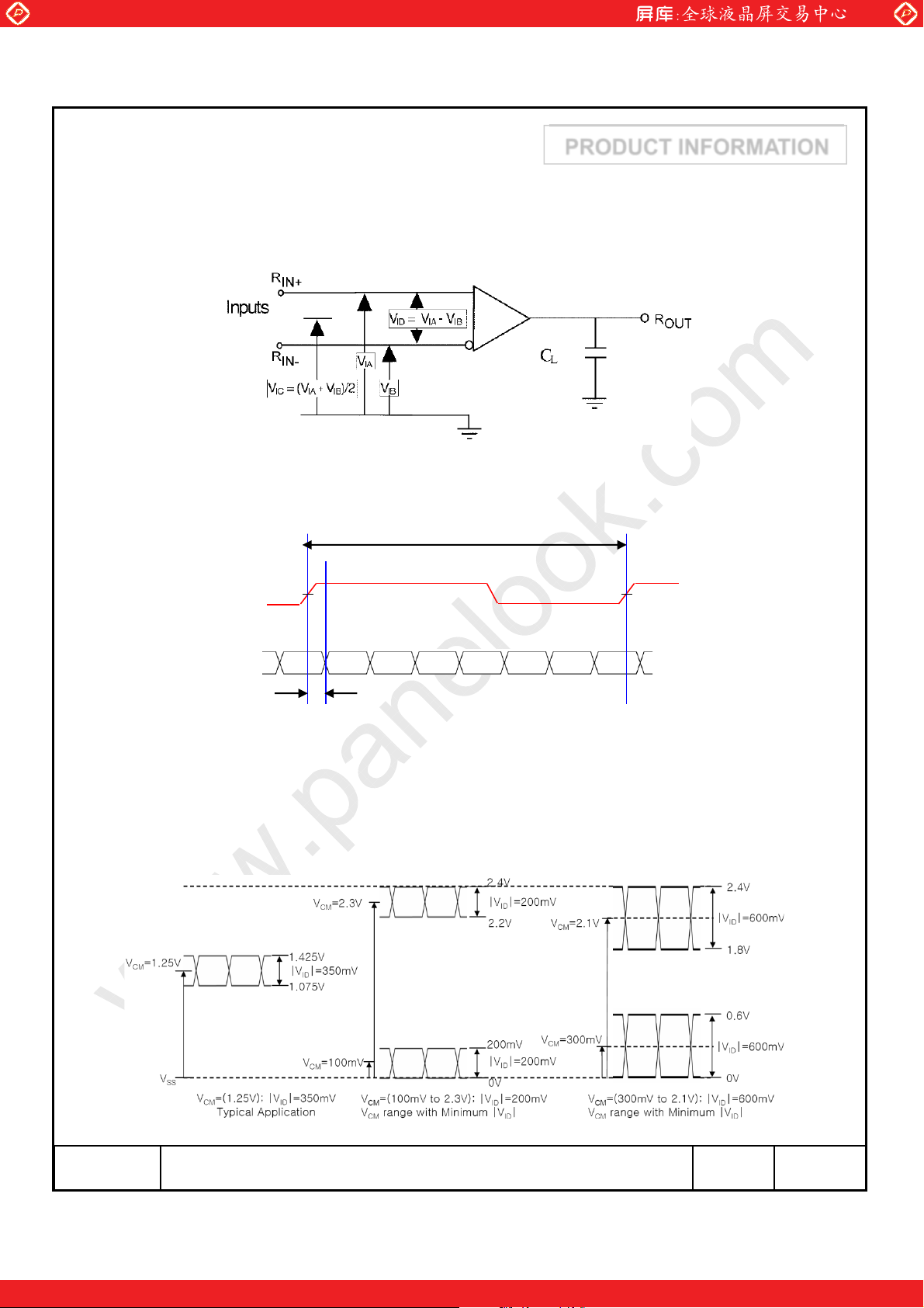
(2) Differential receiver voltage definitions and propagation delay and transition time test circuit
a. All input pulses have frequency = 10MHz, t
includes all probe and fixture capacitance
b. C
L
Note a.
www.panelook.com
or tF=1ns
R
Note b.
PRODUCT INFORMATION
(3) LVDS Receiver DC parameters are measured under static and steady conditions
which may not be reflective of its performance in the end application.
T
LVDS Clk
LVDS Data
RX +/-
V
DIFF
t
SKEW
= 0V
= 0V
V
DIFF
Differential
Differential
where tskew : skew between LVDS clock & LVDS data,
T : 1 period time of LVDS clock
cf) (-/+) of 300psec means LVDS data goes before or after LVDS clock.
(4) Definition of VIDand V
using single-end signals
CM
MODEL LTM215HT04 Page
One step solution for LCD / PDP / OLED panel application: Datasheet, inventory and accessory!
12/33
www.panelook.com
Page 13
Global LCD Panel Exchange Center
(5) fV=60Hz, fDCLK = 67.3MHz, VDD = 5.0V, DC Current.
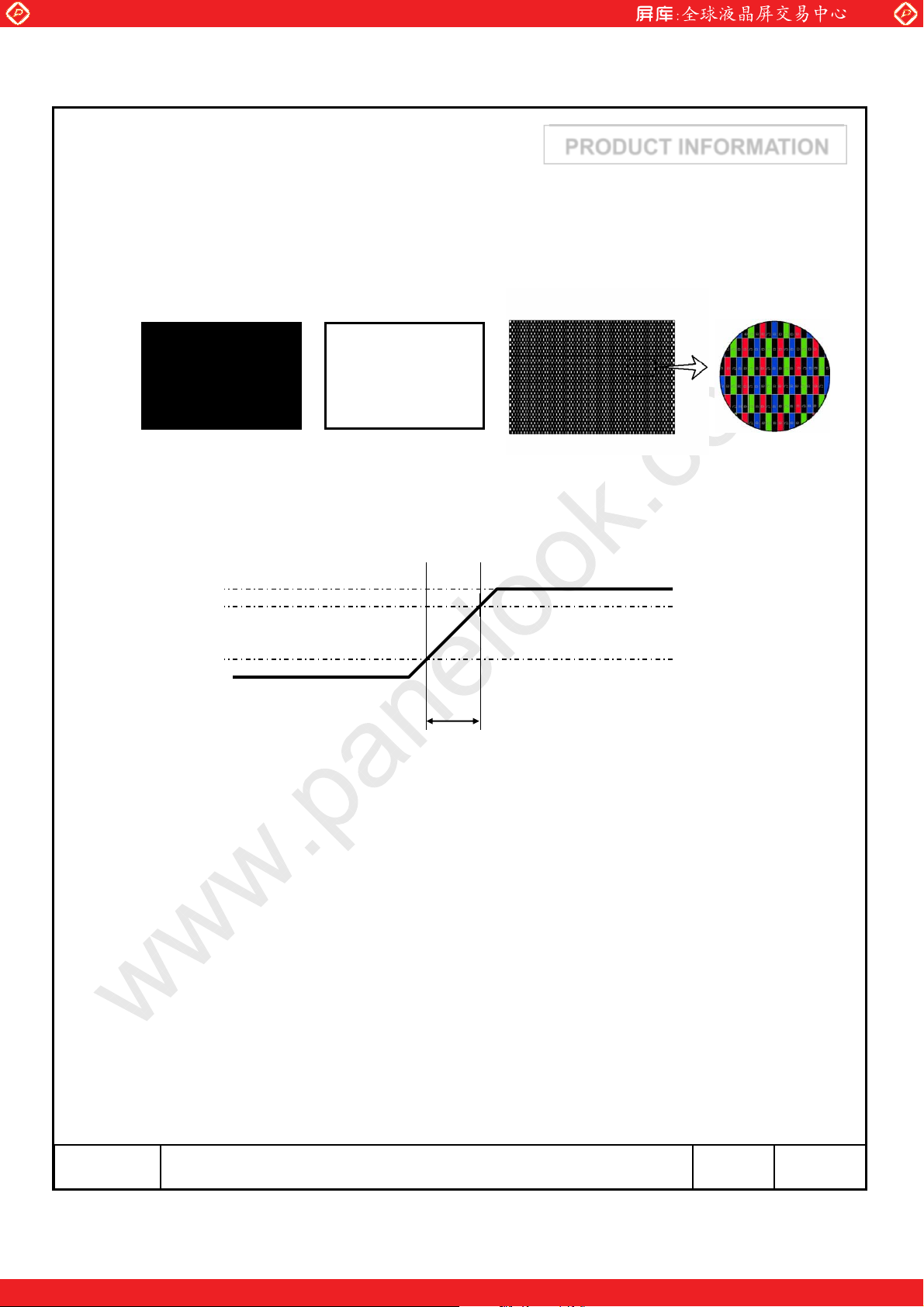
(6) Power dissipation check pattern (LCD Module only)
a) Black Pattern b) White Pattern c) Dot Pattern
www.panelook.com
PRODUCT INFORMATION
(7) Measurement Condition
100%
90%
10%
GND
Rush Current I
T
RUSH
can be measured when T
RUSH
=470༕
RUSH
. is 470༕.
V
DD
MODEL LTM215HT04 Page
One step solution for LCD / PDP / OLED panel application: Datasheet, inventory and accessory!
13/33
www.panelook.com
Page 14
Global LCD Panel Exchange Center
3.2 Back Light Unit
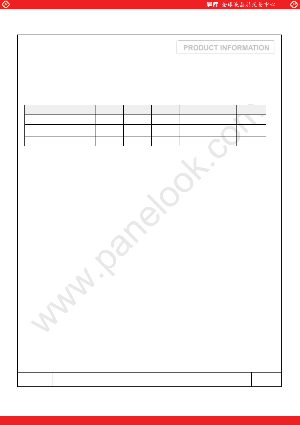
3.2.1 The characteristics of LED bar
The back light unit is composed of WLED.
Item Symbol Min. Typ. Max. Unit Note
www.panelook.com
PRODUCT INFORMATION
Ta=25 · 2¶C
LED Forward Current I
LED Array Voltage V
Operating Life Time Hr 30,000 - - Hour (2)
Note (1) The above specification is not for the converter output, but for the LED bar.
The LED 1-bar consists of 30 LED packages ; 3 parallel X 10 serial
(2) Life time(Hr) is defined as the time when brightness of a LED package itself
becomes 50% or less than its original value at the condition of Ta=25 · 2¶C
and I
=330mA
F
F
P
- 330 - mA /channel
- 33.0 35.0 V -
MODEL LTM215HT04 Page
One step solution for LCD / PDP / OLED panel application: Datasheet, inventory and accessory!
14/33
www.panelook.com
Page 15
Global LCD Panel Exchange Center
www.panelook.com
4. BLOCK DIAGRAM
PRODUCT INFORMATION
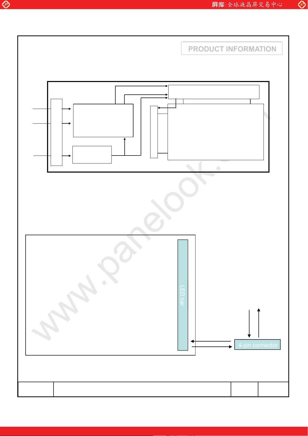
4.1 TFT LCD Module
(USI-2)
Source Driver ICs
Column Driver Circuit
TFT-LCD
LVDS
pair #1
LVDS
pair #2
+5.0V
V
DD
CN1
(30pin)
LVDS (Rx)
(USI -2)(Tx)
Timing Controller
Power
Circuit
Control signal
G1
G1080
S1 S 1920
Control signal
(1920 x RGB x 1080 pixels)
4.2 Back Light Unit
Connector : Molex 104086-0410(4-pin connector) or equivalent
(mating CNT : Molex 104085-0400, 104085-0410 or equivalent)
LED bar
LED Power
LED Return
signal
LED Power
LED Return
4-pin connector
signal
For detail connector information, please refer to page 23.
MODEL LTM215HT04 Page
One step solution for LCD / PDP / OLED panel application: Datasheet, inventory and accessory!
15/33
www.panelook.com
Page 16
Global LCD Panel Exchange Center
www.panelook.com
5. Input Terminal Pin Assignment
PRODUCT INFORMATION
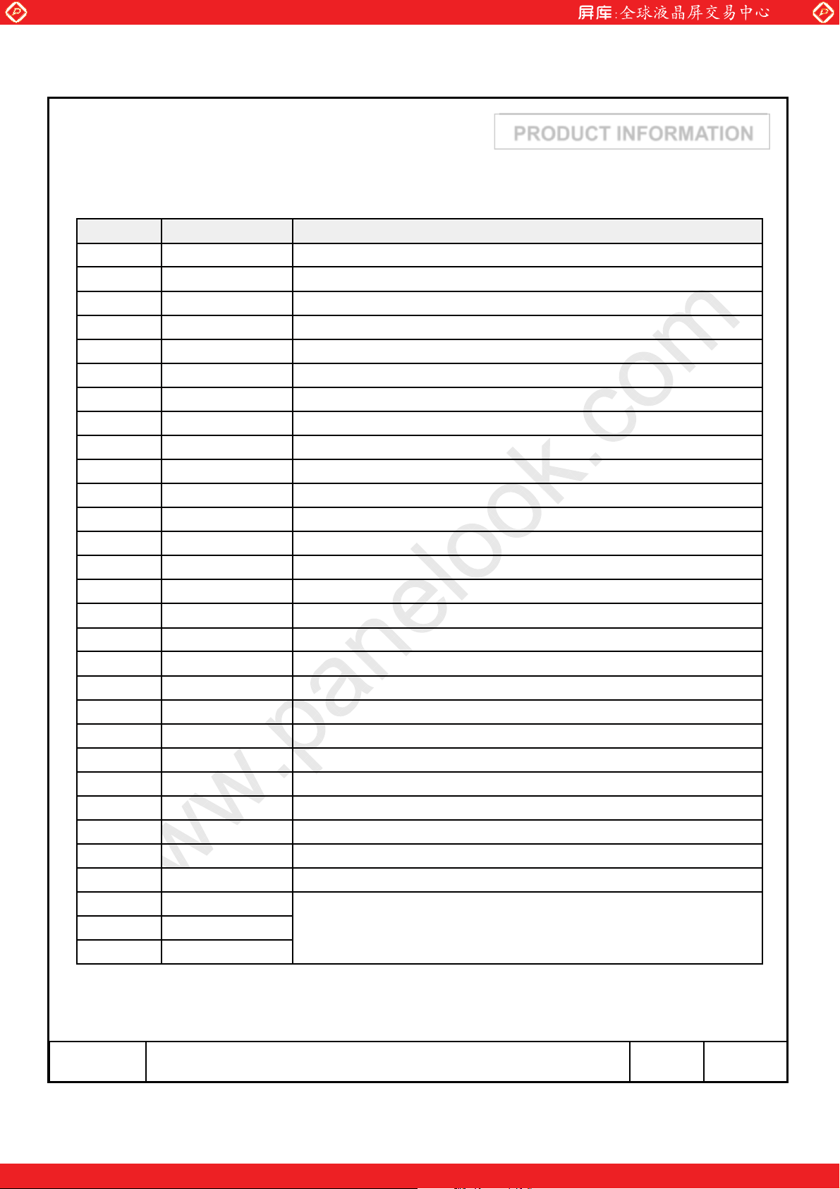
5.1. Input Signal & Power ( Connector : P TWO 196308-30041 or equivalent )
PIN NO SYMBOL FUNCTION
1 RXO0- Negative LVDS differential data output 0 (ODD data)
2 RXO0+ Positive LVDS differential data output 0 (ODD data)
3 RXO1- Negative LVDS differential data output 1(ODD data)
4 RXO1+ Positive LVDS differential data output 1 (ODD data)
5 RXO2- Negative LVDS differential data output 2 (ODD data)
6 RXO2+ Positive LVDS differential data output 2 (ODD data)
7 GND Ground
8 RXOC- Negative Sampling Clock (ODD data)
9 RXOC+ Positive Sampling Clock (ODD data)
10 RXO3- Negative LVDS differential data output 3 (ODD data)
11 RXO3+ Positive LVDS differential data output 3 (ODD data)
12 RXE0- Negative LVDS differential data output 0 (EVEN data)
13 RXE0+ Positive LVDS differential data output 0 (EVEN data)
14 GND Ground
15 RXE1- Negative LVDS differential data output 1 (EVEN data)
16 RXE1+ Positive LVDS differential data output 1 (EVEN data)
17 GND Ground
18 RXE2- Negative LVDS differential data output 2 (EVEN data)
19 RXE2+ Positive LVDS differential data output 2 (EVEN data)
20 RXEC- Negative Sampling Clock (EVEN data)
21 RXEC+ Positive Sampling Clock (EVEN data)
22 RXE3- Negative LVDS differential data output 3 (EVEN data)
23 RXE3+ Positive LVDS differential data output 3 (EVEN data)
24 GND Ground
25 NC * CE (For LCD internal use only. Do not connect)
26 NC * CTL (For LCD internal use only. Do not connect)
27 NC No Connection
28 VDD
Power Supply : +5V29 VDD
30 VDD
MODEL LTM215HT04 Page
One step solution for LCD / PDP / OLED panel application: Datasheet, inventory and accessory!
16/33
www.panelook.com
Page 17
Global LCD Panel Exchange Center
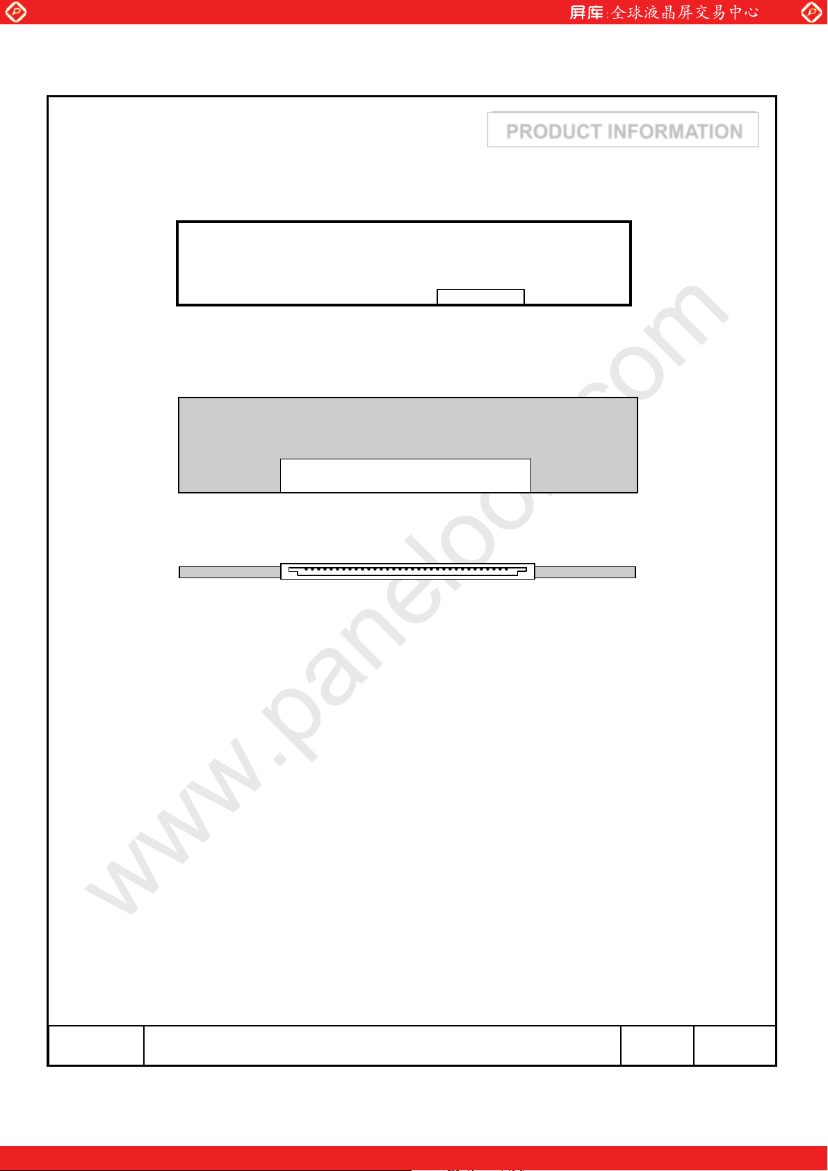
Note) Pin number starts from Left side
www.panelook.com
PRODUCT INFORMATION
PCB
Pin No. 1 Pin No. 30
#30#1
P TWO 196308-30041 or equivalent
Fig. Connector diagram
a. All GND pins should be connected together and also be connected
to the LCD’s metal chassis.
b. All power input pins should be connected together.
c. All NC pins should be separated from other signal or power.
MODEL LTM215HT04 Page
One step solution for LCD / PDP / OLED panel application: Datasheet, inventory and accessory!
17/33
www.panelook.com
Page 18
Global LCD Panel Exchange Center
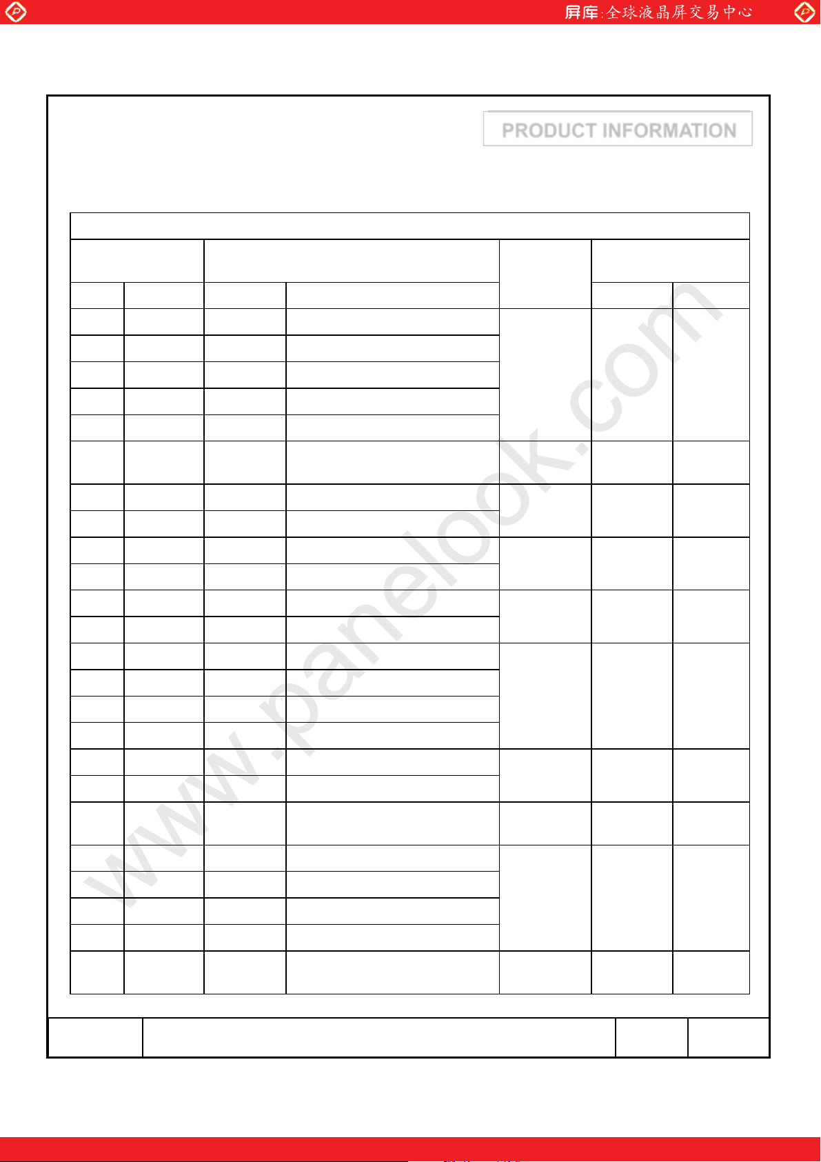
5.2 LVDS Interface (1)
5.2.1 Odd Pixel Data (1st pixel data)
LVDS Transmitter ( DS90C383, DS90C385 ) Signal Interface
www.panelook.com
PRODUCT INFORMATION
Device Input Pin Device Input Signal
No Symbol Symbol Function Terminal Symbol
51 TXIN0 RO0 Red Odd Pixel Data (LSB)
52 TXIN1 RO1 Red Odd Pixel Data
54 TXIN2 RO2 Red Odd Pixel Data
55 TXIN3 RO3 Red Odd Pixel Data
56 TXIN4 RO4 Red Odd Pixel Data
2 TXIN5 RO7 Red Odd Pixel Data (MSB)
3 TXIN6 RO5 Red Odd Pixel Data
4 TXIN7 GO0 Green Odd Pixel Data (LSB)
6 TXIN8 GO1 Green Odd Pixel Data
7 TXIN9 GO2 Green Odd Pixel Data
8 TXIN10 GO6 Green Odd Pixel Data
10 TXIN11 GO7 Green Odd Pixel Data (MSB)
Output
Signal
TXOUT0-
TXOUT0+
TXOUT3-
TXOUT3+
TXOUT0-
TXOUT0+
TXOUT1-
TXOUT1+
TXOUT3-
TXOUT3+
To LTM215HT04
Interface (CN1 )
No. 1
No. 2
No. 10
No. 11
No. 1
No. 2
No. 3
No. 4
No. 10
No. 11
RXO0-
RXO0+
RXO3-
RXO3+
RXO0-
RXO0+
RXO1-
RXO1+
RXO3-
RXO3+
11 TXIN12 GO3 Green Odd Pixel Data
12 TXIN13 GO4 Green Odd Pixel Data
14 TXIN14 GO5 Green Odd Pixel Data
15 TXIN15 BO0 Blue Odd Pixel Data (LSB)
16 TXIN16 BO6 Blue Odd Pixel Data
18 TXIN17 BO7 Blue Odd Pixel Data (MSB)
19 TXIN18 BO1 Blue Odd Pixel Data
20 TXIN19 BO2 Blue Odd Pixel Data
22 TXIN20 BO3 Blue Odd Pixel Data
23 TXIN21 BO4 Blue Odd Pixel Data
24 TXIN22 BO5 Blue Odd Pixel Data
50 TXIN27 RO6 Red Odd Pixel Data
TXOUT1-
TXOUT1+
TXOUT3-
TXOUT3+
TXOUT1-
TXOUT1+
TXOUT2-
TXOUT2+
TXOUT3-
TXOUT3+
No. 3
No. 4
No. 10
No. 11
No. 3
No. 4
No. 5
No. 6
No. 10
No. 11
MODEL LTM215HT04 Page
RXO1-
RXO1+
RXO3-
RXO3+
RXO1-
RXO1+
RXO2-
RXO2+
RXO3-
RXO3+
18/33
One step solution for LCD / PDP / OLED panel application: Datasheet, inventory and accessory!
www.panelook.com
Page 19
Global LCD Panel Exchange Center
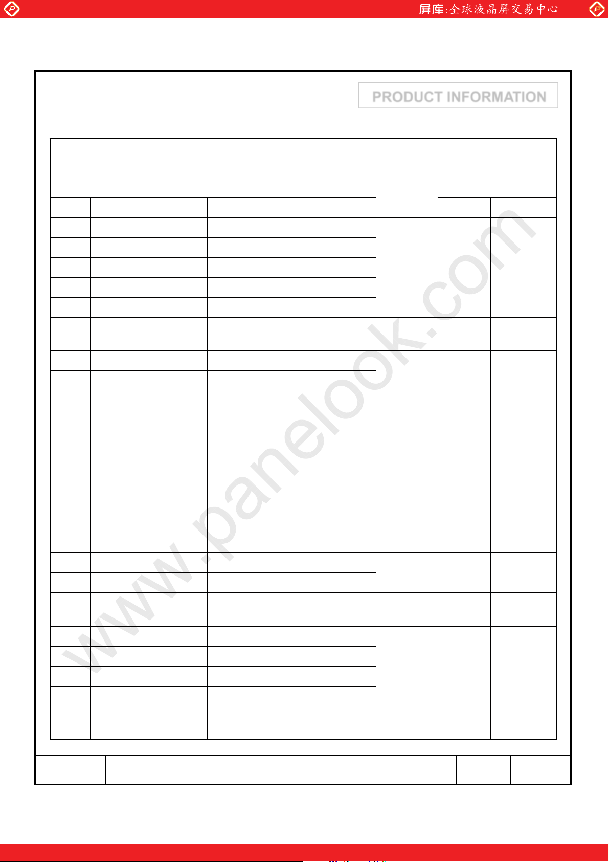
5.2.2 Even Pixel Data (2nd pixel data)
LVDS Transmitter ( DS90C383, DS90C385 ) Signal Interface
www.panelook.com
PRODUCT INFORMATION
Device Input Pin Device Input Signal
No Symbol Symbol Function Terminal Symbol
51 TXIN0 RE0 Red Even Pixel Data (LSB)
52 TXIN1 RE1 Red Even Pixel Data
54 TXIN2 RE2 Red Even Pixel Data
55 TXIN3 RE3 Red Even Pixel Data
56 TXIN4 RE4 Red Even Pixel Data
2 TXIN5 RE7 Red Even Pixel Data (MSB)
3 TXIN6 RE5 Red Even Pixel Data
4 TXIN7 GE0 Green Even Pixel Data (LSB)
6 TXIN8 GE1 Green Even Pixel Data
7 TXIN9 GE2 Green Even Pixel Data
8 TXIN10 GE6 Green Even Pixel Data
10 TXIN11 GE7 Green Even Pixel Data (MSB)
Output
Signal
TXOUT0-
TXOUT0+
TXOUT3-
TXOUT3+
TXOUT0-
TXOUT0+
TXOUT1-
TXOUT1+
TXOUT3-
TXOUT3+
To LTM215HT04
Interface (CN1 )
No. 12
No. 13
No. 22
No. 23
No. 12
No. 13
No. 15
No. 16
No. 22
No. 23
RXE0-
RXE0+
RXE3-
RXE3+
RXE0-
RXE0+
RXE1-
RXE1+
RXE3-
RXE3+
11 TXIN12 GE3 Green Even Pixel Data
12 TXIN13 GE4 Green Even Pixel Data
14 TXIN14 GE5 Green Even Pixel Data
15 TXIN15 BE0 Blue Even Pixel Data (LSB)
16 TXIN16 BE6 Blue Even Pixel Data
18 TXIN17 BE7 Blue Even Pixel Data (MSB)
19 TXIN18 BE1 Blue Even Pixel Data
20 TXIN19 BE2 Blue Even Pixel Data
22 TXIN20 BE3 Blue Even Pixel Data
23 TXIN21 BE4 Blue Even Pixel Data
24 TXIN22 BE5 Blue Even Pixel Data
50 TXIN27 RE6 Red Even Pixel Data
TXOUT1-
TXOUT1+
TXOUT3-
TXOUT3+
TXOUT1-
TXOUT1+
TXOUT2-
TXOUT2+
TXOUT3-
TXOUT3+
No. 15
No. 16
No. 22
No. 23
No. 15
No. 16
No. 18
No. 19
No. 22
No. 23
MODEL LTM215HT04 Page
RXE1-
RXE1+
RXE3-
RXE3+
RXE1-
RXE1+
RXE2-
RXE2+
RXE3-
RXE3+
19/33
One step solution for LCD / PDP / OLED panel application: Datasheet, inventory and accessory!
www.panelook.com
Page 20
Global LCD Panel Exchange Center
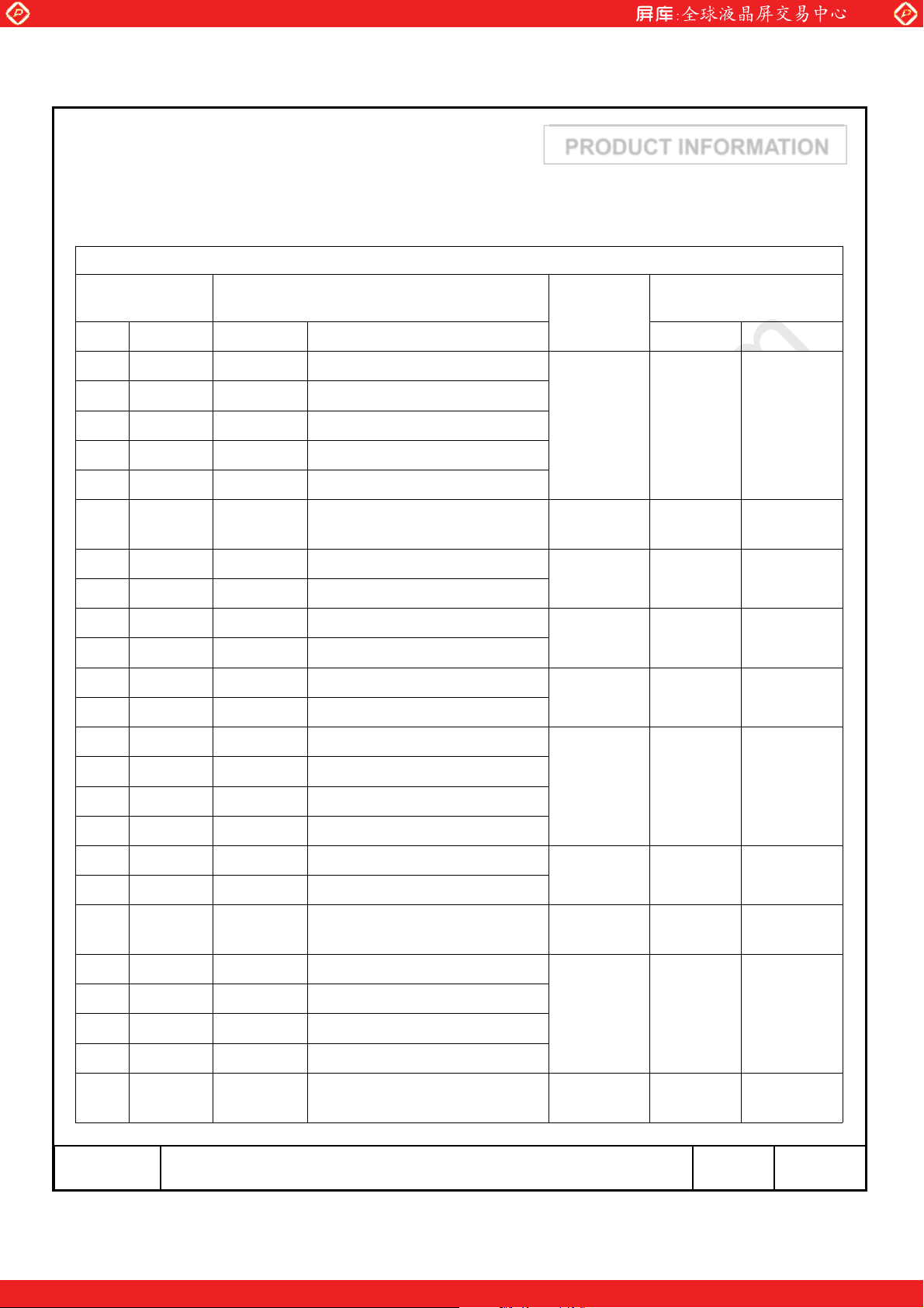
5.2 LVDS Interface (2)
5.2.3 Odd Pixel Data (1st pixel data)
LVDS Transmitter ( DS90C387 ) Signal Interface
www.panelook.com
PRODUCT INFORMATION
Device Input Pin Device Input Signal
No Symbol Symbol Function Terminal Symbol
10 R10 RO0 Red Odd Pixel Data (LSB)
9 R11 RO1 Red Odd Pixel Data
8 R12 RO2 Red Odd Pixel Data
7 R13 RO3 Red Odd Pixel Data
6 R14 RO4 Red Odd Pixel Data
3 R17 RO7 Red Odd Pixel Data (MSB)
5 R15 RO5 Red Odd Pixel Data
2 G10 GO0 Green Odd Pixel Data (LSB)
1 G11 GO1 Green Odd Pixel Data
100 G12 GO2 Green Odd Pixel Data
94 G16 GO6 Green Odd Pixel Data
93 G17 GO7 Green Odd Pixel Data (MSB)
Output
Signal
A0M
A0P
A3M
A3P
A0M
A0P
A1M
A1P
A3M
A3P
To LTM215HT04
Interface (CN1 )
No. 1
No. 2
No. 10
No. 11
No. 1
No. 2
No. 3
No. 4
No. 10
No. 11
RXO0-
RXO0+
RXO3-
RXO3+
RXO0-
RXO0+
RXO1-
RXO1+
RXO3-
RXO3+
99 G13 GO3 Green Odd Pixel Data
96 G14 GO4 Green Odd Pixel Data
95 G15 GO5 Green Odd Pixel Data
92 B10 BO0 Blue Odd Pixel Data (LSB)
86 B16 BO6 Blue Odd Pixel Data
85 B17 BO7 Blue Odd Pixel Data (MSB)
91 B11 BO1 Blue Odd Pixel Data
90 B12 BO2 Blue Odd Pixel Data
89 B13 BO3 Blue Odd Pixel Data
88 B14 BO4 Blue Odd Pixel Data
87 B15 BO5 Blue Odd Pixel Data
4 R16 RO6 Red Odd Pixel Data
A1M
A1P
A3M
A3P
A1M
A1P
A2M
A2P
A3M
A3P
No. 3
No. 4
No. 10
No. 11
No. 3
No. 4
No. 5
No. 6
No. 10
No. 11
MODEL LTM215HT04 Page
RXO1-
RXO1+
RXO3-
RXO3+
RXO1-
RXO1+
RXO2-
RXO2+
RXO3-
RXO3+
20/33
One step solution for LCD / PDP / OLED panel application: Datasheet, inventory and accessory!
www.panelook.com
Page 21
Global LCD Panel Exchange Center
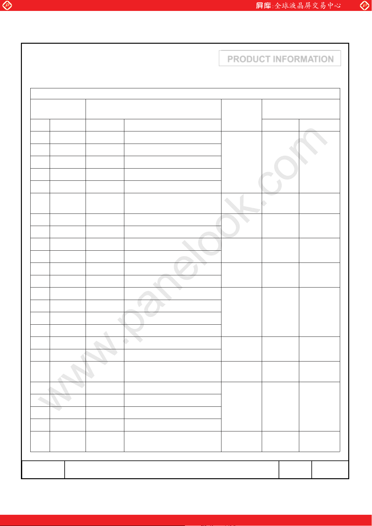
5.2.4 Even Pixel Data (2nd pixel data)
LVDS Transmitter ( DS90C387 ) Signal Interface
www.panelook.com
PRODUCT INFORMATION
Device Input Pin Device Input Signal
No Symbol Symbol Function Terminal Symbol
84 R20 RE0 Red Even Pixel Data (LSB)
81 R21 RE1 Red Even Pixel Data
80 R22 RE2 Red Even Pixel Data
79 R23 RE3 Red Even Pixel Data
78 R24 RE4 Red Even Pixel Data
75 R27 RE7 Red Even Pixel Data (MSB)
77 R25 RE5 Red Even Pixel Data
74 G20 GE0 Green Even Pixel Data (LSB)
73 G21 GE1 Green Even Pixel Data
72 G22 GE2 Green Even Pixel Data
66 G26 GE6 Green Even Pixel Data
65 G27 GE7 Green Even Pixel Data (MSB)
Output
Signal
A4M
A4P
A7M
A7P
A4M
A4P
A5M
A5P
A7M
A7P
To LTM215HT04
Interface (CN1 )
No. 12
No. 13
No. 22
No. 23
No. 12
No. 13
No. 15
No. 16
No. 22
No. 23
RXE0+
RXE3+
RXE0+
RXE1+
RXE3+
RXE0-
RXE3-
RXE0-
RXE1-
RXE3-
71 G23 GE3 Green Even Pixel Data
70 G24 GE4 Green Even Pixel Data
69 G25 GE5 Green Even Pixel Data
64 B20 BE0 Blue Even Pixel Data (LSB)
58 B26 BE6 Blue Even Pixel Data
57 B27 BE7 Blue Even Pixel Data (MSB)
63 B21 BE1 Blue Even Pixel Data
62 B22 BE2 Blue Even Pixel Data
61 B23 BE3 Blue Even Pixel Data
60 B24 BE4 Blue Even Pixel Data
59 B25 BE5 Blue Even Pixel Data
76 R26 RE6 Red Even Pixel Data
A5M
A5P
A7M
A7P
A5M
A5P
A6M
A6P
A7M
A7P
No. 15
No. 16
No. 22
No. 23
No. 15
No. 16
No. 18
No. 19
No. 22
No. 23
MODEL LTM215HT04 Page
RXE1-
RXE1+
RXE3-
RXE3+
RXE1-
RXE1+
RXE2-
RXE2+
RXE3-
RXE3+
21/33
One step solution for LCD / PDP / OLED panel application: Datasheet, inventory and accessory!
www.panelook.com
Page 22
Global LCD Panel Exchange Center
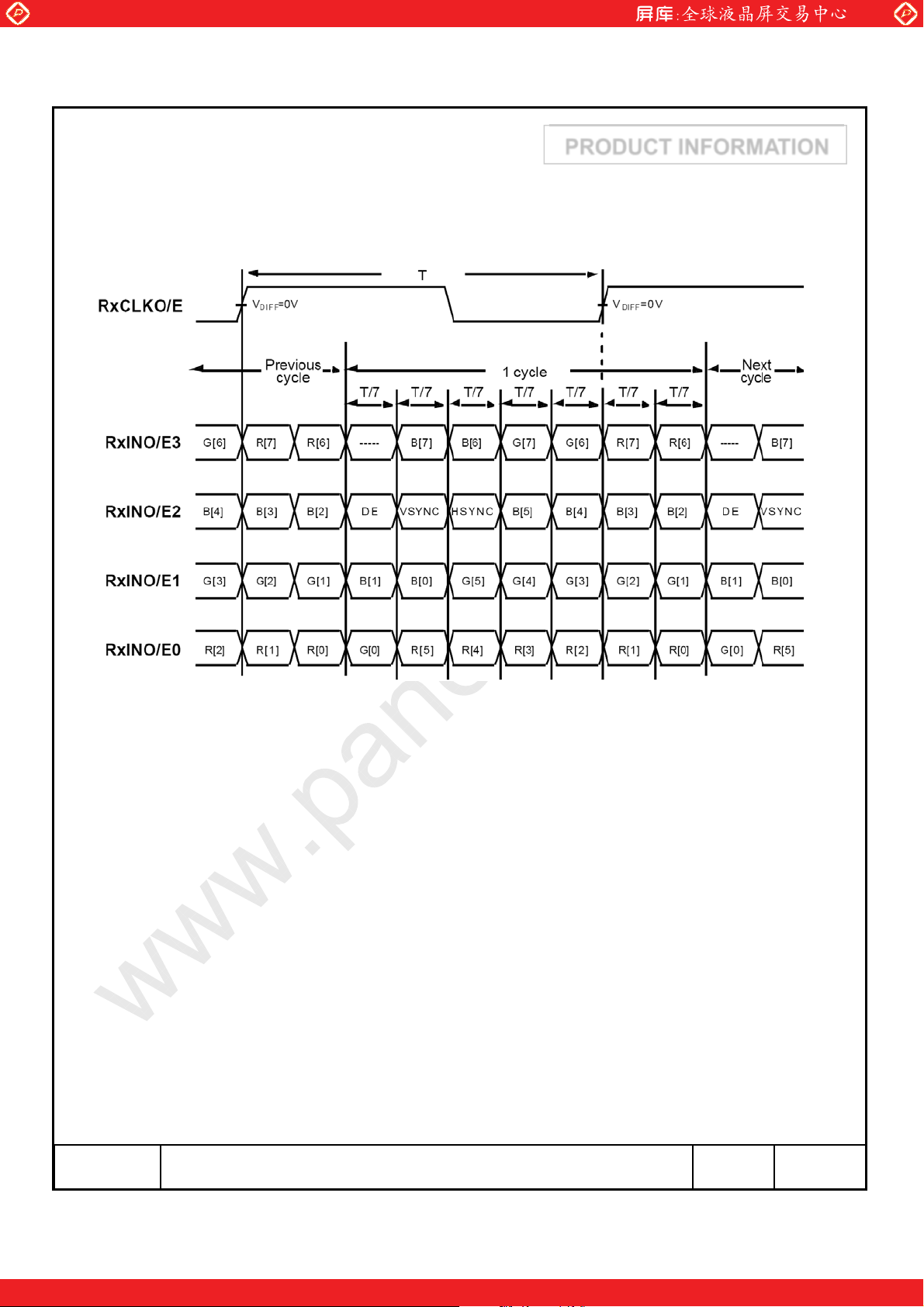
5.2.5 Timing Diagrams of LVDS For Transmitting
LVDS Receiver : Integrated T-CON
www.panelook.com
PRODUCT INFORMATION
MODEL LTM215HT04 Page
One step solution for LCD / PDP / OLED panel application: Datasheet, inventory and accessory!
22/33
www.panelook.com
Page 23
Global LCD Panel Exchange Center
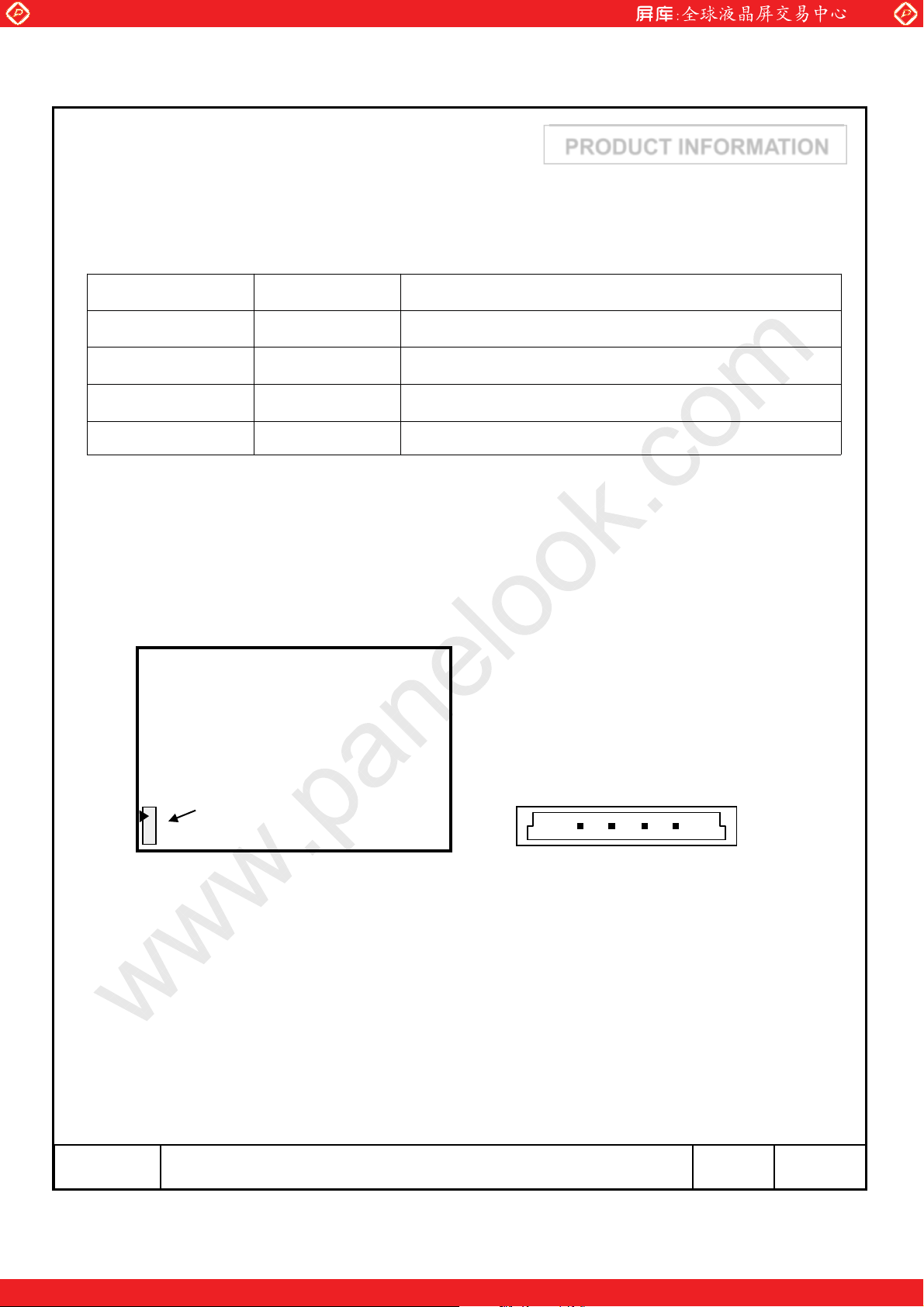
5.3 Back Light Unit
LED Bar input connector : Molex 104086-0410 or equivalent
(mating CNT : Molex 104085-0400, 104085-0410 or equivalent)
Pin No. Pin description Function
1 Vin LED power input
2 RTN 1 LED Bar return channel 1
3 RTN 2 LED Bar return channel 2
4 RTN 3 LED Bar return channel 3
www.panelook.com
PRODUCT INFORMATION
Note ) Pin number starts from Left side
Rear view of panel
Connector
#4
Fig. Connector diagram
#1
MODEL LTM215HT04 Page
One step solution for LCD / PDP / OLED panel application: Datasheet, inventory and accessory!
23/33
www.panelook.com
Page 24
Global LCD Panel Exchange Center
COLOR
DISPLAY
(8bit)
GRAY
SCALE
LEVEL
R0R1R2R3R4R5R6
R7
G0G1G2G3G4G5G6
G7
B0B1B2B3B4B5B6
B7
BASIC
COLOR
BLACK
00000000000000000000000
0
-
BLUE
00000000000000001111111
1
-
GREEN
00000000111111110000000
0
-
CYAN
00000000111111111111111
1
-
RED
11111111000000000000000
0
-
MAGENTA
11111111000000001111111
1
-
YELLOW
11111111111111110000000
0
-
WHITE
11111111111111111111111
1
-
GRAY
SCALE
OF RED
BLACK
00000000000000000000000
0
R0
DARK
LIGHT
10000000000000000000000
0
R1
01000000000000000000000
0
R2
:::::::::::::::::
:
R3~
R252
:::::::::::::::::
:
10111111000000000000000
0
R253
01111111000000000000000
0
R254
RED
11111111000000000000000
0
R255
GRAY
SCALE
OF GRE
EN
BLACK
00000000000000000000000
0
G0
DARK
LIGHT
00000000100000000000000
0
G1
00000000010000000000000
0
G2
:::::::::::::::::
:
G3~
G252
:::::::::::::::::
:
00000000101111110000000
0
G253
00000000011111110000000
0
G254
GREEN
00000000111111110000000
0
G255
GRAY
SCALE
OF BLU
BLACK
00000000000000000000000
0
B0
DARK
LIGHT
00000000000000001000000
0
B1
00000000000000000100000
0
B2
:::::::::::::::::
:
B3~
B242
:::::::::::::::::
:
00000000000000001011111
1
B253
00000000000000000111111
1
B254
BLUE
00000000000000001111111
1
B255
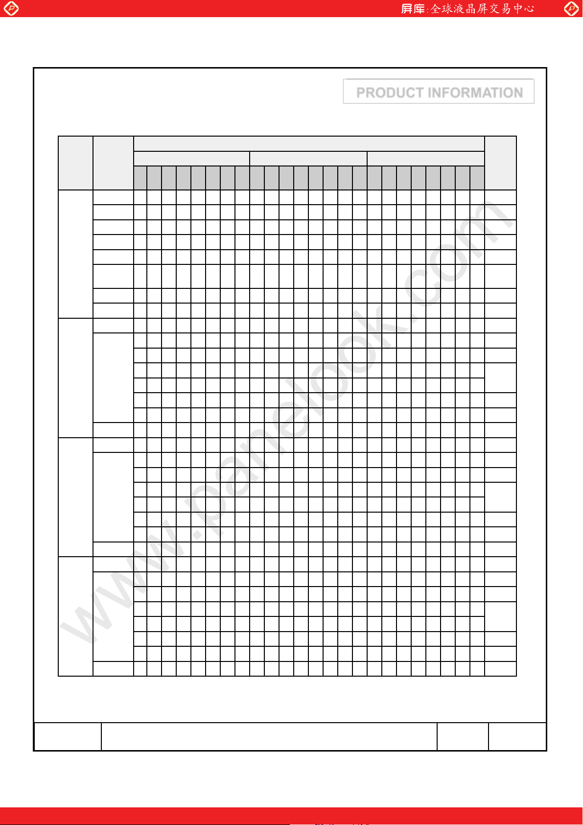
5.4 Input Signals, Basic Display Colors and Gray Scale of Each Color
RED GREEN BLUE
www.panelook.com
PRODUCT INFORMATION
DATA SIGNAL
↑
↓
↑
↓
↑
E
↓
Note (1) Definition of Gray :
Rn : Red Gray, Gn : Green Gray, Bn : Blue Gray (n = Gray level)
Input Signal : 0 = Low level voltage, 1 = High level voltage
One step solution for LCD / PDP / OLED panel application: Datasheet, inventory and accessory!
MODEL LTM215HT04 Page
24/33
www.panelook.com
Page 25
Global LCD Panel Exchange Center
www.panelook.com
6. Interface Timing
PRODUCT INFORMATION
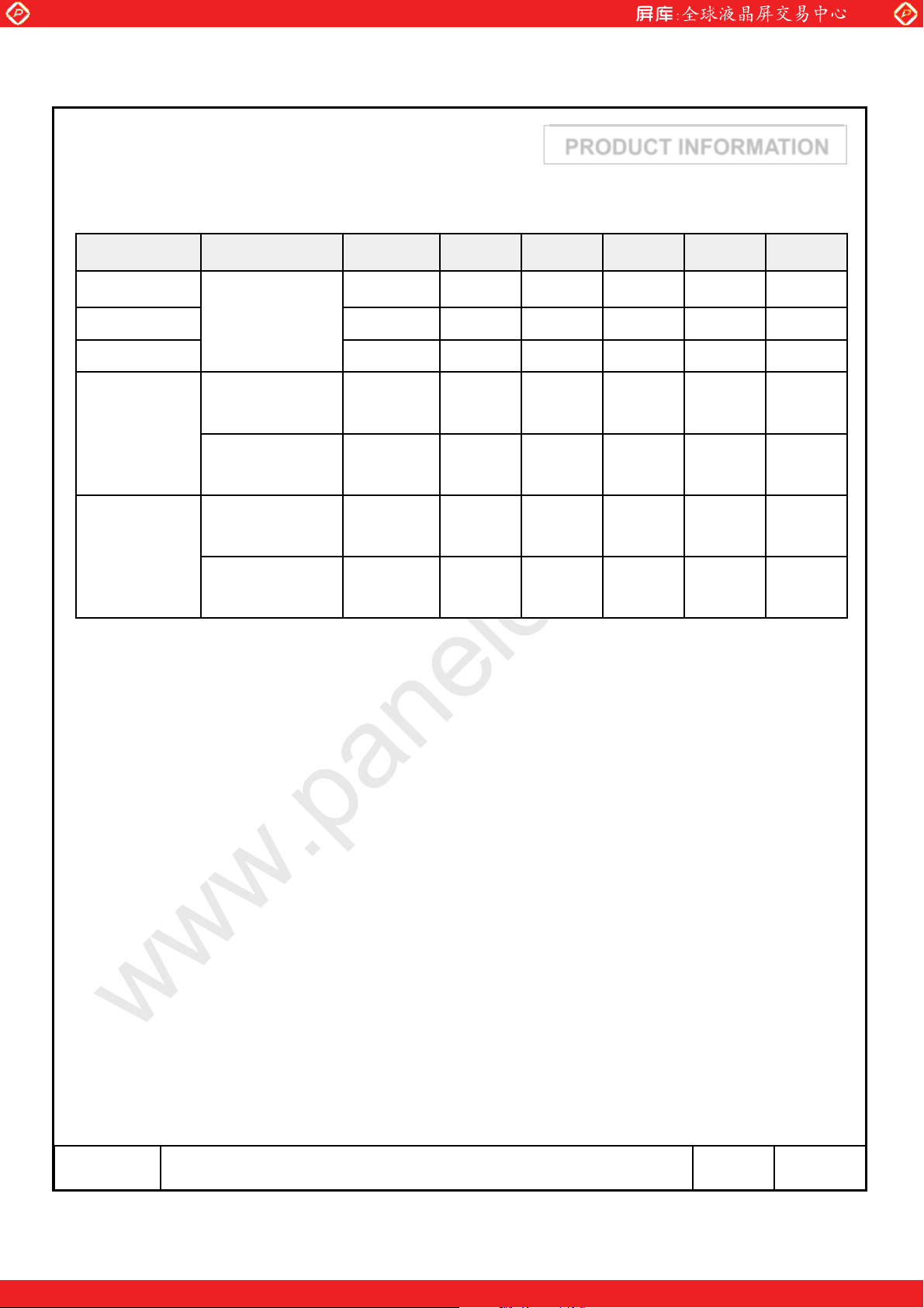
6.1 Timing Parameters( DE mode )
SIGNAL ITEM SYMBOL MIN. TYP. MAX. Unit NOTE
Clock
Hsync F
Frequency
Vsync F
Active
Vertical
Display Period
Display Term
Vertical Total T
Active Display
Horizontal
Period
Display Term
Horizontal Total T
1/T
T
T
H
V
VD
V
HD
H
C
56.4 67.3 87.5 MHz -
54.2 66.0 83.8 KHz -
49 60 75 Hz -
1080 1080 1080 lines -
1105 1111 1118 lines -
960 960 960 clocks
990 1010 1040 clocks
2pixel
/clock
2pixel
/clock
Note (1) This product is DE only mode. The input of Hsync & Vsync signal does
not have an effect on normal operation.
(2) Test Point : TTL control signal and CLK at LVDS Tx input terminal in system
(3) Internal Vcc = 5.0V
MODEL LTM215HT04 Page
One step solution for LCD / PDP / OLED panel application: Datasheet, inventory and accessory!
25/33
www.panelook.com
Page 26
Global LCD Panel Exchange Center
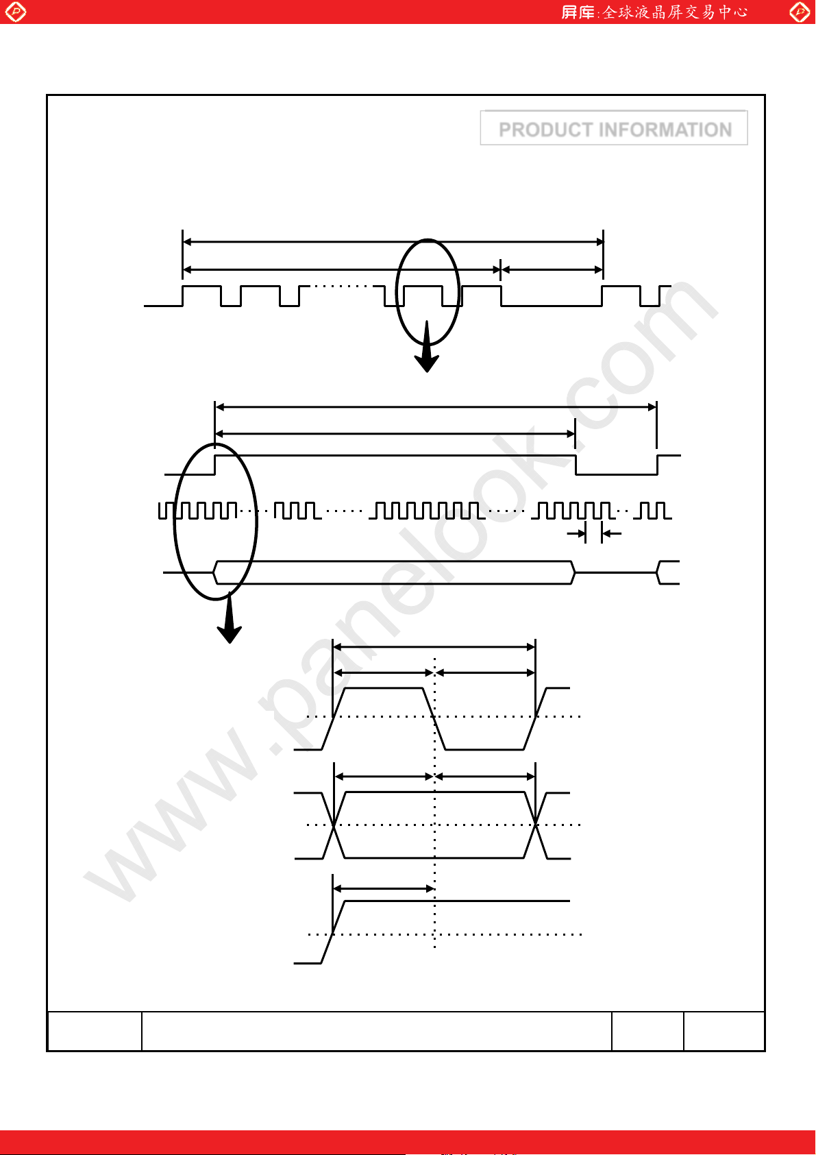
6.2 Timing diagrams of interface signal ( DE only mode )
www.panelook.com
PRODUCT INFORMATION
TV
DE
DE
DCLK
DATA
SIGNALS
TVD
TVB
TH
THD
TC
TC
TCH
DCLK
TDS TDH
DISPLAY
DATA
TES
DE
TCL
0.5
V
0.5
V
0.5
V
CC
CC
CC
MODEL LTM215HT04 Page
26/33
One step solution for LCD / PDP / OLED panel application: Datasheet, inventory and accessory!
www.panelook.com
Page 27
Global LCD Panel Exchange Center
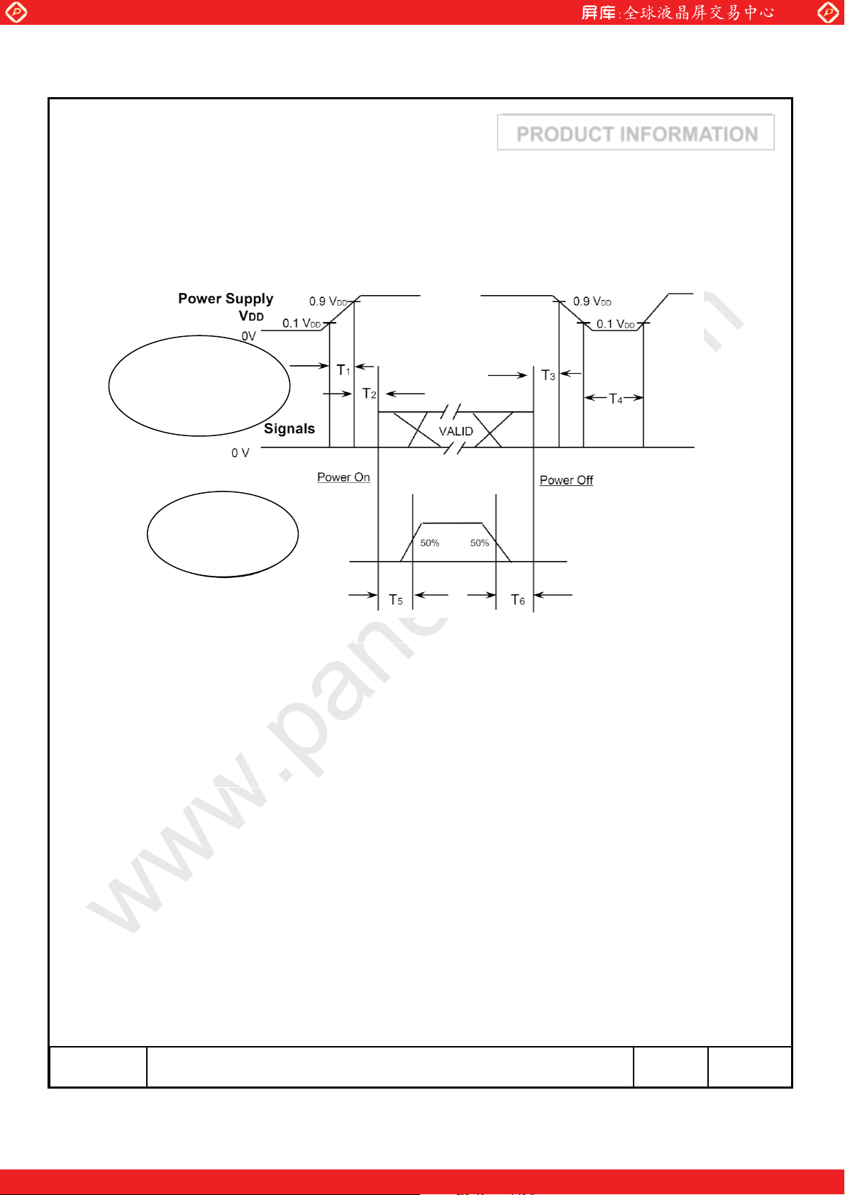
6.3 Power ON/OFF Sequence
To prevent a latch-up or DC operation of the LCD Module, the power on/off
sequence should be as the diagram below.
300༕≤T1≤10msec
0≤T2≤50msec
0≤T3≤50msec
1sec≤T4
www.panelook.com
PRODUCT INFORMATION
Back-Light
(Recommended)
500msec≤T5
100msec≤T6
T1 : VDDrising time from 10% to 90%
T2 : The time from V
T3 : The time from valid data off to V
to valid data at power ON.
DD
off at power Off.
DD
T4 : VDDoff time for Windows restart
T5 : The time from valid data to B/L enable at power ON.
T6 : The time from valid data off to B/L disable at power Off.
The supply voltage of the external system for the Module input should be the same
as the definition of VDD.
Apply the lamp voltage within the LCD operation range. When the back light turns on
before the LCD operation or the LCD turns off before the back light turns off,
the display may momentarily show abnormal screen.
In case of V
= off level,
DD
please keep the level of input signals low or keep a high impedance.
T4 should be measured after the Module has been fully discharged between power off
and on period.
Interface signal should not be kept at high impedance when the power is on.
MODEL LTM215HT04 Page
One step solution for LCD / PDP / OLED panel application: Datasheet, inventory and accessory!
27/33
www.panelook.com
Page 28
Global LCD Panel Exchange Center
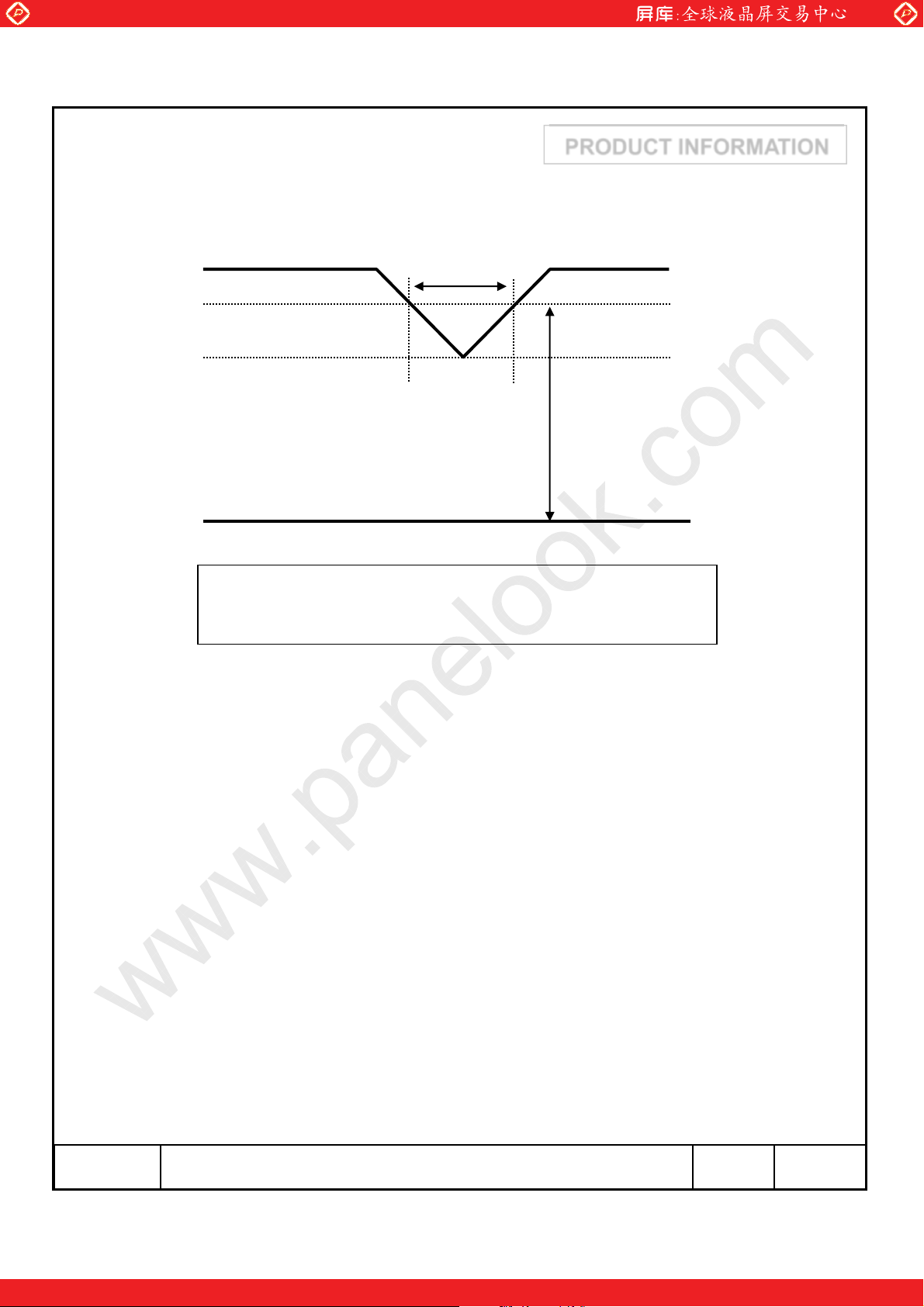
6.4 VDD Power Dip Sequence
V
DD
90%
www.panelook.com
T
d
PRODUCT INFORMATION
80%
V
CC
GND
4.5V ≤ VDD≤ 5.5V
If V
(typ.) x 80% ≤ VCC≤ VDD(typ) x 90%
DD
Then, 0<Td ≤20msec
Note (1) The above conditions are for the glitch of the input voltage.
(2) For stable operation of an LCD Module power, please follow them.
i.e., if typ VDD x 80% ≤ Vcc ≤ typ VDD x 90%, then Tdshould be less than 20ms.
MODEL LTM215HT04 Page
One step solution for LCD / PDP / OLED panel application: Datasheet, inventory and accessory!
28/33
www.panelook.com
Page 29
Global LCD Panel Exchange Center
www.panelook.com
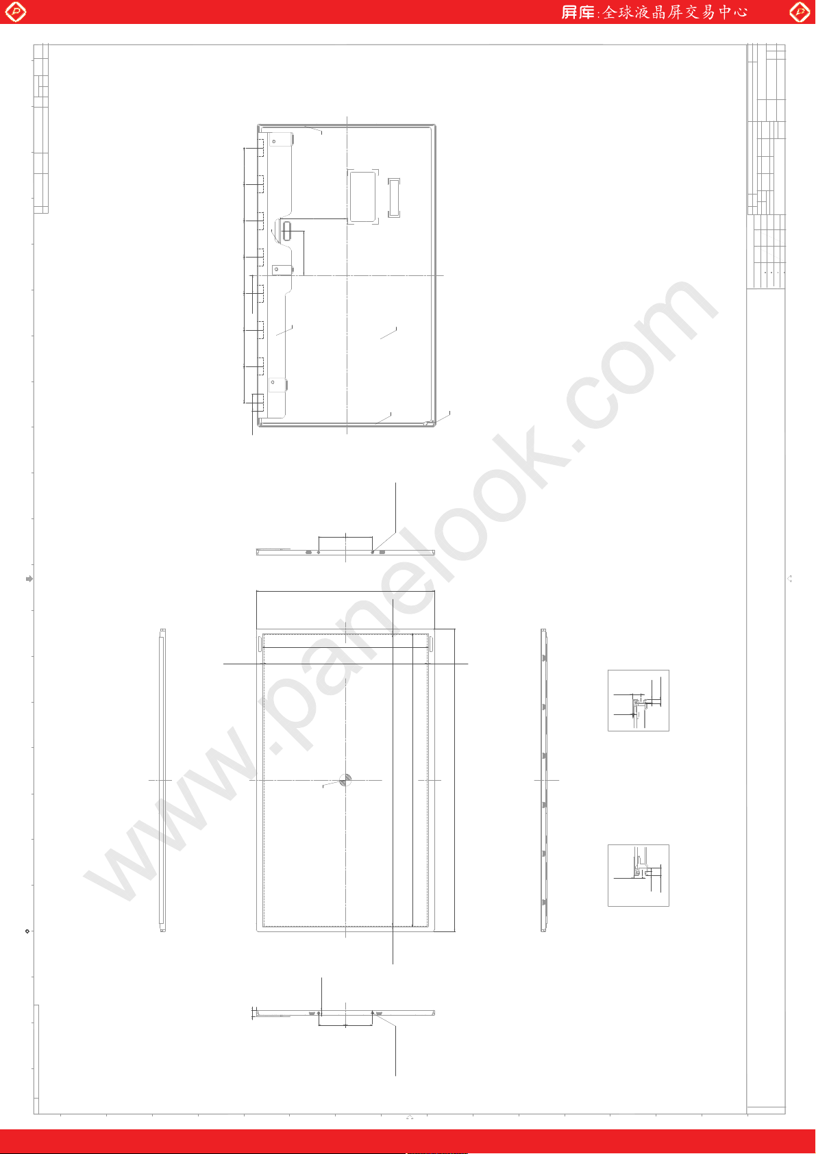
7. Outline Dimension
[ Refer to the next page ]
PRODUCT INFORMATION
MODEL LTM215HT04 Page
One step solution for LCD / PDP / OLED panel application: Datasheet, inventory and accessory!
29/33
www.panelook.com
Page 30
Global LCD Panel Exchange Center
\
ylthyr
|umvs klkG kptU G
vmU Gth{l yphs
th{l yphs
~lpno{
mpupzo
xN{
zwljpmpjh{pvu
jvklGuv
why{Guhtl
uv
x y z { | } ~
\`U ] \`U ] \`U ] \`U ] \`U ] \`U ] \`U ]
Y_U Y Y`U _
www.panelook.com
V
WW
XGX
G
zoll{
s{tYX\o{W[TjWXVWYGs lk
v|{ sp ulTk p tU
jvklGuvU }lyU G
tvkls Guhtl
why{Vzoll{
GGGuhtl
zwljUG uv
T^U ^
X
W
_
puw|{Gjvuulj{vyGmpyz{wpu
^YU \
XUGihjrspno{GaG~op{lGslk
QG uv{lz
YUGslkGjvuulj{vyGzwljpmpjh{pvuU
GGGTGthrlyaGtvsl
GGGTGwhy{GuvUGaGXW[W_]W[XWG
GGGGGGvyG
GGGGG
ZUGpVmGjvuulj{vyV~pylGzwljpmpjh{pvuU
GGGTGthrlyGaG|q|
GGGTGwhy{GuvGaGzXWWTsZWvTjYZG[UG|zlyGtv|u{punG{vyx|lGzwljGaGZG¥G[GT
TXWU Y
T^U W
T^U ^
T_U X
jorN kGi hwwN kGi|up{
klzN kGi
~zUG rpt
XXUW XUXY
kyhN uGi
V
zhtz|unGlslj{yvup jz
·XU W
{vslyhujl
zjhsl
yl}GGGGGkh{lGGGGGGGGGG
GGGGGGGGGGGGGGGGGGGGklzjypw{pvuGvmGyl}pzpvuGGGGGGGGGGGGGGGGGGGGylhzvuGGGGGGGGGGGGGGGGGGGGjonNkGi
nlulyhsG{vslyhujl
z{lwGGGGGGsl}lsGXGGsl}lsGYGGsl}lsGZ
WGcGGcG[GGGG·WUW\GGGG·WUXGGGGGG·WUYGG
[GcGGcGX]GGG·WUW_GGGG·WUX\GGGGG·WUZ
X]GcG GcG][GG G·WUXYG GGG ·WUY\G GGG G·WU\
][GcGGcGY\]GG·WUY\GGGG·WU[GGGGGG·WU_
stuvw
n o p q r
YTtZG z
k G t G Y U X
[
[
·
·
[
[
W
W
U
U
Z
Z
Y
`
Y
U
Y
W
·
U
G
\
v
|
{
z
G
p
l
XU ] ·WU \
^
Y
X
U
Z
i
G
l
l
s
G
v
w
l
u
]
X
·
U
W
]
U
\
l
G
h
y
h
l
Y
_
U
X
X
G
j
h
{
p
}
[^`U _G illsG vwlu
[^]U ][G hj{p }lG hylh
X
U
·
]
W
U
\
YU X
YU Z\
[
[
U
W
\
U
[`\U ]·WU \ G v|{G zp l
hj{p }lG jlu{ly
[
U
[
YU X
ZU ]
XU ] ·WU \
[U [ ·WU Z
·
·
[
[
W
W
[
[
U
U
Z
XWUY·WU\
h i j k l m
mps lGuvU
^
\
One step solution for LCD / PDP / OLED panel application: Datasheet, inventory and accessory!
^
W
]
\
]
W
\
\
Z
YTtZG z
k G t G Z U \
\
[
\
W
[
\
W
Z
W
Z
Y
\
Y
W
\
X
pvu
W
X
yl}pz
W
www.panelook.com
Page 31
Global LCD Panel Exchange Center
www.panelook.com
8. General Precautions
PRODUCT INFORMATION
8.1 Handling
(a) When the module is assembled, it should be attached to the system firmly
using all mounting holes. Be careful not to twist and bend the module.
(b) Because the inverter uses high voltages, it should be disconnected from power
source before it is assembled or disassembled.
(c) Refrain from strong mechanical shock and / or any force to the module.
In addition to damage, it may cause improper operation or damage to the module
and LED back light.
(d) Note that polarizer films are very fragile and could be damaged easily.
Do not press or scratch the surface harder than a HB pencil lead.
(e) Wipe off water droplets or oil immediately. If you leave the droplets for a long
time, staining or discoloration may occur.
(f) If the surface of the polarizer is dirty, clean it using absorbent cotton or soft cloth.
(g) Desirable cleaners are water, IPA (Isopropyl Alcohol) or Hexane.
Do not use Ketone type materials (ex. Acetone), Ethyl alcohol, Toluene, Ethyl acid
or Methyl chloride. It might cause permanent damage to the polarizer due to chemical
reaction.
(h) If the liquid crystal material leaks from the panel, it should be kept away
from the eyes or mouth . In case of contact with hands, legs or clothes, it must
be washed away with soap thoroughly.
(i) Protect the Module from static, or the CMOS Gate Array IC would be damaged.
(j) Use finger-stalls with soft gloves in order to keep display clean during the
incoming inspection and assembly process.
(k) Do not disassemble the Module.
(l) Do not adjust the variable resistor located on the Module.
(m) Protection film for polarizer on the Module should be slowly peeled off just
before use so that the electrostatic charge can be minimized.
(n) Pins of I/F connector should not be touched directly with bare hands.
MODEL LTM215HT04 Page
One step solution for LCD / PDP / OLED panel application: Datasheet, inventory and accessory!
31/33
www.panelook.com
Page 32
Global LCD Panel Exchange Center
8.2 Storage
(a) Do not leave the Module in high temperature, and high humidity for a long time.
It is highly recommended to store the Module with temperature from 5 to 40
and relative humidity of less than 70%.
(b) Do not store the TFT-LCD Module in direct sunlight.
(c) The Module should be stored in a dark place. It is prohibited to apply sunlight or
fluorescent light in storing.
(d) Storage period is recommended not to exceed 1 year.
www.panelook.com
PRODUCT INFORMATION
8.3 Operation
(a) Do not connect or disconnect the Module in the "Power On" condition.
(b) Power supply should always be turned on/off by the item 6.3
"Power on/off sequence"
(c) Module has high frequency circuits. Sufficient suppression to the electromagnetic
interference should be done by system manufacturers. Grounding and shielding
methods may be important to minimize the interference.
8.4 Operation Condition Guide
(a) The LCD product should be operated under normal conditions.
Normal condition is defined as below;
- Temperature : 20·15
- Humidity : 65·20%
- Display pattern : continually changing pattern (Not stationary)
(b) If the product will be used in extreme conditions such as high temperature,
humidity, display patterns or operation time etc.., It is strongly recommended
to contact SEC for Application engineering advice. Otherwise, its reliability and
function may not be guaranteed. Extreme conditions are commonly found at
Airports, Transit Stations, Banks, Stock market, and Controlling systems.
MODEL LTM215HT04 Page
One step solution for LCD / PDP / OLED panel application: Datasheet, inventory and accessory!
32/33
www.panelook.com
Page 33
Global LCD Panel Exchange Center
8.5 Others
(a) Ultra-violet ray filter is necessary for outdoor operation.
(b) Avoid condensation of water. It may result in improper operation or disconnection
of electrode.
(c) Do not exceed the absolute maximum rating value. ( supply voltage variation,
input voltage variation, variation in part contents and environmental temperature,
and so on)
Otherwise the Module may be damaged.
www.panelook.com
PRODUCT INFORMATION
(d) If the Module keeps displaying the same pattern for a long period of time,
the image may be "stuck" to the screen.
To avoid image sticking, it is recommended to use a screen saver.
(e) This Module has its circuitry PCB's on the rear side and should be handled
carefully in order not to be stressed.
(f) Please contact SEC in advance when you display the same pattern for a long time.
MODEL LTM215HT04 Page
One step solution for LCD / PDP / OLED panel application: Datasheet, inventory and accessory!
33/33
www.panelook.com
 Loading...