

Page 1

Toshiba Matsushita Display Technology Co., Ltd
PRODUCT INFORMATION
FEATURES
(1) 15.4WIDE-XGA(1280x800 pixels) display size for notebook PC
(2) LVDS interface system (H-Sync, V-Sync)
MECHANICAL SPECIFICATIONS
Item Specifications
Dimensional Outline (typ.) 344.5max(W) x 222.5max (H) x 6.5max(D) mm
Number of Pixels 1280(W) x 800(H) pixels
Active Area 332.2 (W) x 207.6(H) mm
Pixel Pitch 0.2595(W) x 0.2595(H)
Weight (approximately) 585 g(Max)
Backlight Single CCFL, Sidelight type
ABSOLUTE MAXIMUM RATINGS
Item Symbol Min. Max. Unit Checked Terminal
Supply Voltage VDD -0.3 +4.0 V VDD – GND
Input Voltage of Signals VIN -0.3 VDD+0.3 V LVDS interface
Operating Ambient Temperature TOP 0 50
Operating Ambient Humidity HOP 10 90 %(RH)
Storage Temperature T
Storage Humidity H
Operating Temperature for Panel - 0 +60
ELECTRICAL SPECIFICATION(T.B.D)
Item Symbol Min. Typ. Max. Unit Remarks
Supply Voltage 1)
www.jxlcd.com
FL Start Voltage (Ta=0°C) V
Differential Input Voltage
Common Mode Input Voltage 2) VCM 1.0 - 2.4 –(VID)/2 V
Power Consumption --- (6.6) --- W IFL=6.0 mA(rms)
*1) The module should be always operated within these ranges. The "Typ." shows the recommendable value.
*2) Recommended LVDS transmitter: DS90CF365
OPTICAL SPECIFICATION (Ta=25°C)(T.B.D)
Item Min. Typ. Max. Unit Remarks
Contrast Ratio (CR) (150) (400) --- ---
Response Time (tON+ t
Luminance (L) (150) (190) --- cd/m2 IFL=6.0mA(rms)
www.jxlcd.com
2)
VID 100 - 600 mV
OFF
VDD 3.0 3.3 3.6 V
VFL --- (920) --- V(rms) IFL=6.0mA(rms)
TBD --- TBD V(rms)
SFL
IDD --- (335) --- mA Current Consumption
IFL --- 6.0 6.0 mA(rms)
) --- --- 40 ms @25deg
-20 +60
STG
10 90 %(RH)
STG
39cm COLOUR TFT-LCD MODULE
(15.4 WIDE TYPE)
LTD154EX0S (Z)
(p-Si TFT)
TENTATIVE
°C
°C
°C
Brack <=> White
*The information contained herein is presented only as a guide for the applications of our products. No responsibility is assumed by
Toshiba Matsushita Display Technology or other rights of the third parties which may result from its use. No license is granted by
implication or otherwise under any patent or patent rights of Toshiba Matsushita Display Technology or others.
*The information contained herein may be changed without prior notice. It is therefore advisable to contact Toshiba Matsushita Display
Technology before proceeding with the design of equipment incorporating this product.
(1/11) 2003-06-30 (Ver.0.1)
Page 2
198+/-0
.
2
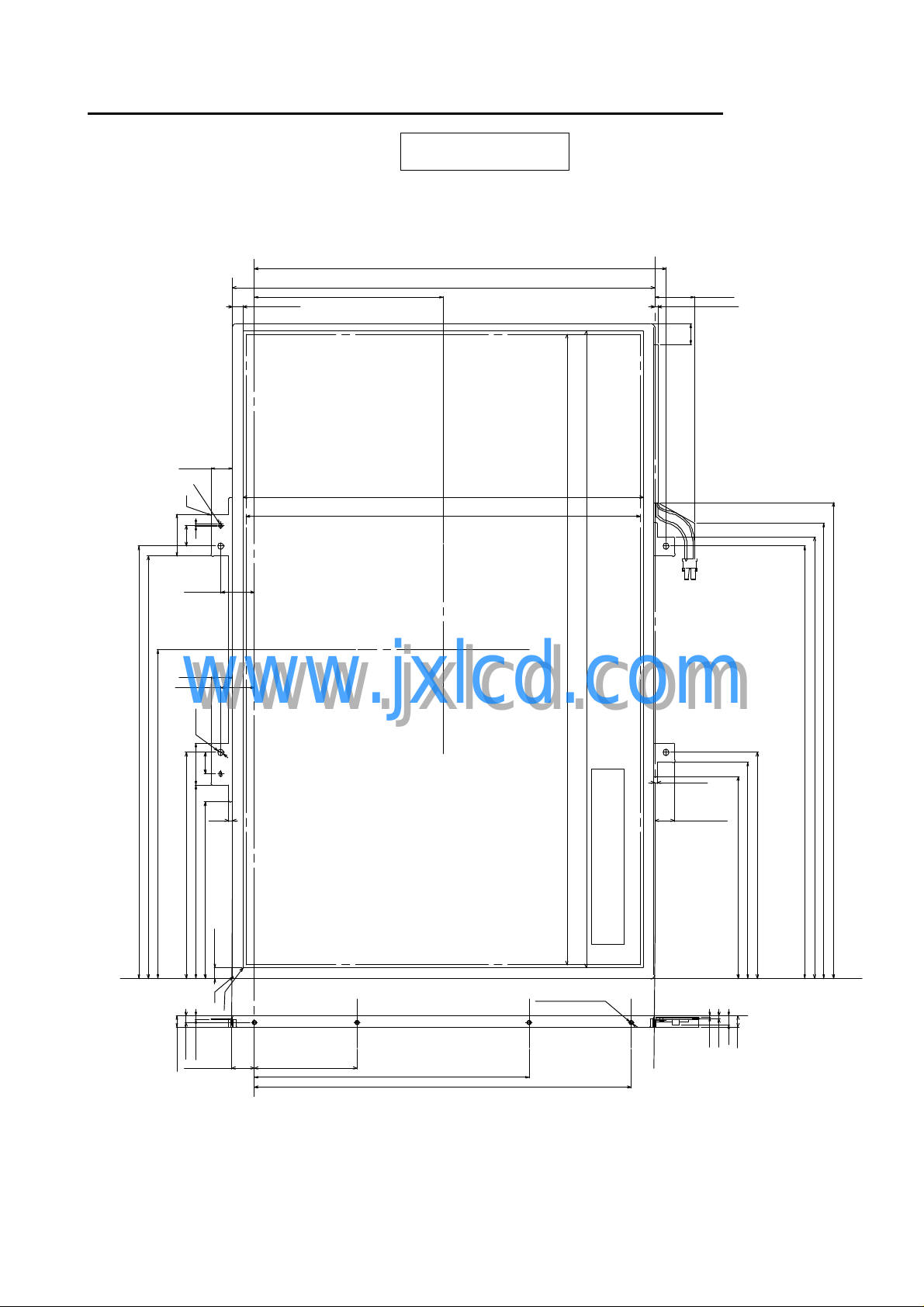
DIMENSIONAL OUTLINE
(Front side)
11+/-0.3
5
7
.
0
R
-
R1
2
22
11
11
LTD154LX0S (Z)
Unit : mm
TENTATIVE
.15
216
2
2
99.15
5.65+/-0.2
.
2
+/-
0
2
210.7
207.6
Standard tolerance : ±0.5
Max
)
22(
)
Max
2.5
(
11+/-1
FL Connector : JST BHSR-02VS-1
I/F Connector : JAE FI-XB30SRL-HF11
INV. Connedtor : HONDA LVC-D20SYG
Note
HJST
12
Standard Tolerance : +/-0.5mm
17.85
332.2
335+/-0.2
11+/-0.3
17.85
www.jxlcd.com
www.jxlcd.com
φ
4- 3.2
227
222
11
22
172.8
1.7
118.6
101.6
92.8
TENTATIVE
5.3+/-0.2
R2
R0.5
M2(Depth 2.5Max)
255(Max)
232
240(Max)
1.7
10.5+/-0.3
118.6
113.6
106
227
4.7
6.1
1.8
3.7+/-0.2
2.1+/-0.2
6.5(Max)
11.85+/-0.2
54+/-0.2
2
/-0
.
.3+
144
0.7
(2/11) 2003-06-30 (Ver.0.1)
Page 3
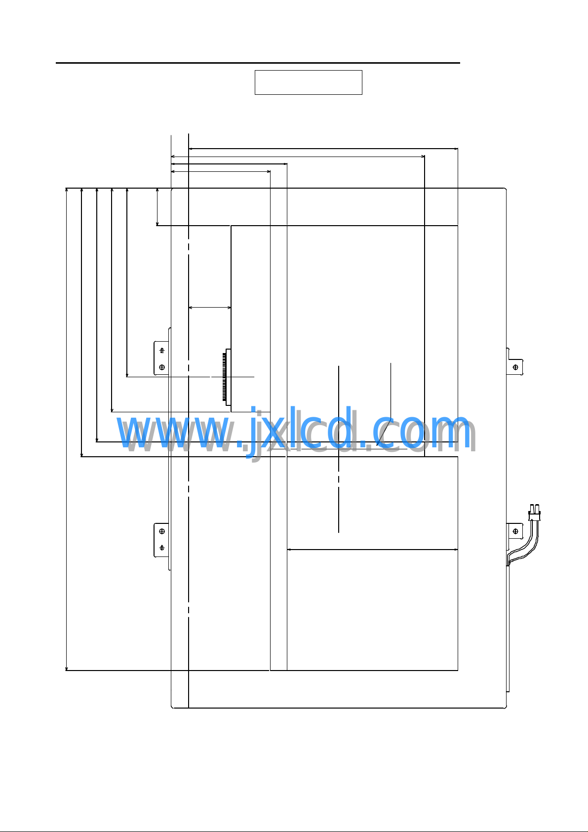
DIMENSIONAL OUTLINE
(Back side)
25(Max)
125.1+/-1
148.1
166.8(Min)
178.8(Max)
LTD154LX0S (Z)
TENTATIVE
Unit : mm
Standard tolerance : ±0.5
n
)
76. 9
65.9
-
1
+
/
2
8
5.7(Max)
167. 8
178(M
i
Light G uide taper surface +0.8
319(Min)
www.jxlcd.com
www.jxlcd.com
1 2
HJST
6.5(Max)
6.5(Max)
5.7(max)
5.9- 4.7( Max)(L ight Gide tape r surfac e)
(3/11) 2003-06-30 (Ver.0.1)
Page 4
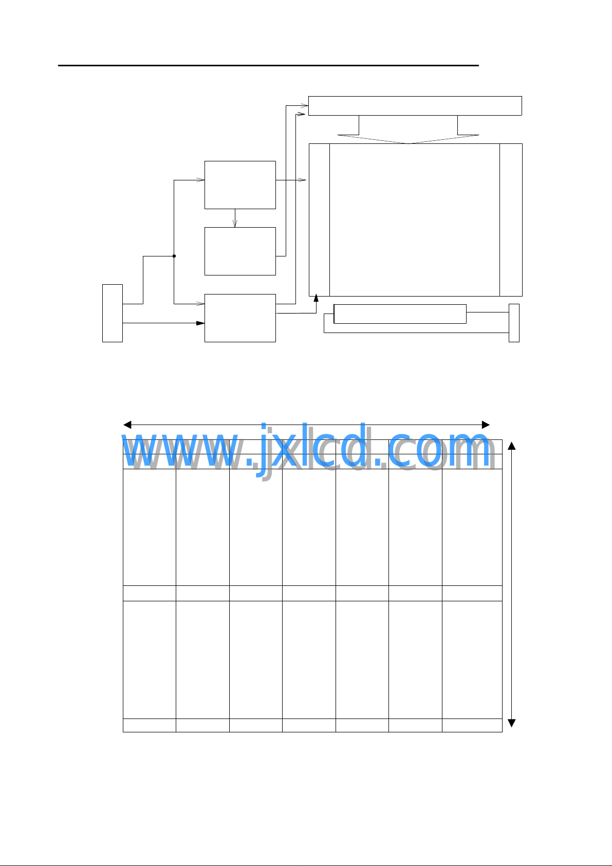
BLOCK DIAGRAM
C N 1
Connector
1, 1 2, 1 X2
1, 2
www.jxlcd.com
www.jxlcd.com
DC/ DC
conv erte r
G ra y s ca l e
Ma ni p u l at io n
Vo l ta ge
Ge n er at i o n
Ci r cu it
Pane l
Controller
LVDS
Gate driver
1280 pixels
, 1 X2n, 1 1280, 1
n-1
LTD154LX0S (Z)
Sour ce driv er
Liqu id Crys tal Pan el
1280 x 800 pixels
Gate driver
Bac kligh t
C N 1
1, Y X
1, 800 1280,800
(4/11) 2003-06-30 (Ver.0.1)
, Y X2n, Y
2n-1
800 pixels
Page 5

TIMING CHART(T.B.D)
tv
tvw
VSYNC
tvsu tvhd th
HSYNC
tv‚†p tvbp tvd
tvds
DE 1023 1024 1 2
LTD154LX0S (Z)
thw
HSYNC thbp
thfp thds thd
thblank
www.jxlcd.com
DE
pixel
CLK
www.jxlcd.com
th
1024
2 3 41
tc
(5/11) 2003-06-30 (Ver.0.1)
Page 6

LTD154LX0S (Z)
TIMING SPECIFICATION
(T.B.D)
Item Symbol min. typ. max. unit
Horizontal Active pixel - - 1280 - Pixels
H Sync Front Porch HSO - 4 - Pixels
H Sync Pulse Width HSPW - 4 - Pixels
H Sync Back Porch HBO - 112 - Pixels
Horizontal Total Pixels - - 1400 - Pixels
Horizontal Blank Pixel - - 120 - Pixels
Horizontal Total Time - - 20 - Us
Horizontal Blank Time - - 1.7 - Us
Vertical Active Line - - 800 - Lines
V Sync Front Porch VSO - 1 - Lines
V Sync Pulse Width VSPW - 2 - Lines
V Sync Back Porch VBO - 30 - Lines
Vertical Total Line - - 833 - Lines
Vertical Blank Line - - 33 - Lines
Vertical Total Time - - 16.7 - Ms
Vertical Blank Time - - 0.7 - Ms
Pixel Clock - - 70 - MHz
Frame Rate - - 60 - Hz
Note 1) Refer to “Timing Chart” and LVDS specifications by chip vendor.
Note 2) If NCLK is fixed to "H" or "L" level for certain period while VDD is supplied, the panel may be damaged.
Note 3) Please adjust LCD operating signal timing and FL driving frequency, to optimize the display quality.
www.jxlcd.com
There is a possibility that flicker is observed by the interference of LCD operating signal timing and FL driving condition
(especially driving frequency), even if the condition satisfies above timing specifications.
Note 4) Do not make tv, tvhd and tvds fluctuate.
If tv, tvhd, and tvds are fluctuate, the panel displays black.
Note 5) In case of using the long frame period, the deterioration of display quality, noise etc. may be occurred.
Note 6) NCLK count of each Horizontal Scanning Time should be always the same.
V-Blanking period should be “n” X “Horizontal Scanning Time”. (n: integer)
Frame period should be always the same.
www.jxlcd.com
1) 2) 3) 4) 5) 6)
(6/11) 2003-06-30 (Ver.0.1)
Page 7

LTD154LX0S (Z)
CONNECTOR PIN ASSIGNMENT FOR INTERFACE
CN1 INPUT SIGNAL
Connector : FI-XB30SR-HF11(Locking Type) / JAPAN AVIATION ELECTRONICS INDUSTRY,LTD.
Mating Connector :
Wire Type:FI-X30H (Housing), FI-XC3-A-15000 (Contact)
FPC Type:FI-X30M or FI-X30M R, Coax Type:FI-X30C or FI-X30C2(Housing), FI-X30CH-7000(Shell)
Terminal No. Symbol Function
1 GND
2
3
4 NC Non-Connection
5 NC Non-Connection
6 NC Non-Connection
7 NC Non-Connection
8 RxOIN0- Odd Negative LVDS differential data input (R0-R5,G0)
9 RxOIN0+ Odd Positive LVDS differential data input (R0-R5,G0)
10 GND
11 RxOIN1- Odd Negative LVDS differential data input (G1-G5, B0-B1)
12 RxOIN1+ Odd Positive LVDS differential data input (G1-G5, B0-B1)
13 GND
14 RxOIN2- Odd Negative LVDS differential data input (B2-B5, HS, VS, DE)
15 RxOIN2+ Odd Positive LVDS differential data input (B2-B5, HS, VS, DE)
16 GND
17 OCLK- Odd Clock Signal(-)
18 OCLK+ Odd Clock Signal(+)
19 GND
20 NC Non-Connection
21 NC Non-Connection
22 NC Non-Connection
23 NC Non-Connection
24 NC Non-Connection
25 NC Non-Connection
26 NC Non-Connection
27 NC Non-Connection
28 NC Non-Connection
www.jxlcd.com
www.jxlcd.com
29 NC Non-Connection
30 NC Non-Connection
Note 1) Please connect GND pin to ground. Don't use it as no-connect nor connection with high impedance.
CN2 CCFL POWER SOURCE
Connector : BHSR-02VS-1 / JAPAN SOLDERLESS TERMINAL MFG CO., LTD.
Mating Connector : SM02B-BHS-1 / JAPAN SOLDERLESS TERMINAL MFG CO., LTD.
Terminal No. Symbol Function
1 VFLH CCFL Power Supply ( high voltage)
2 VFLL CCFL Power Supply (low voltage)
VDD
VDD
Power Supply : +3.3V
Power Supply : +3.3V
(7/11) 2003-06-30 (Ver.0.1)
Page 8

R
RECOMMENDED TRANSMITTER (DS90CF365)
TO LTD154LX0S INTERFACE ASSIGNMENT
Case1: 6bit Transmitter
(DS90CF365)
Input Terminal No. Input Signal
(Graphics controller output signal)
Symbol Terminal Symbol Function
TA0 44 R0 Red Pixels Display Data (LSB)
TA1 45 R1 Red Pixels Display Data
TA2 47 R2 Red Pixels Display Data
TA3 48 R3 Red Pixels Display Data
TA4 1 R4 Red Pixels Display Data
TA5 3 R5 Red Pixels Display Data (MSB)
TA6 4 G0 Green Pixels Display Data (LSB)
TB0 6 G1 Green Pixels Display Data
TB1 7 G2 Green Pixels Display Data
TB2 9 G3 Green Pixels Display Data
TB3 10 G4 Green Pixels Display Data
TB4 12 G5 Green Pixels Display Data (MSB)
TB5 13 B0 Blue Pixels Display Data (LSB)
TB6 15 B1 Blue Pixels Display Data
TC0 16 B2 Blue Pixels Display Data
TC1 18 B3 Blue Pixels Display Data
TC2 19 B4 Blue Pixels Display Data
TC3 20 B5 Blue Pixels Display Data (MSB)
TC4 22 HSYNC Horizontal Synchronization Signal
TC5 23 VSYNC Vertical Synchronization Signal
TC6 25 DE Compound Synchronization Signal
CLK IN 26 CLK Data Sampling Clock TCLK-
www.jxlcd.com
www.jxlcd.com
Output
Symbol
TATA+
TBTB+
TCTC+
TCLK+
Signal
LTD154LX0S (Z)
LTM154LX0S (Z)
Interface
(CN1)
Terminal Symbol
No.5
No.6
No.8
No.9
No.11
No.12
No.14
No.15
RxIN0RxIN0+
RxIN1RxIN1+
RxIN2RxIN2+
CLKCLK+
R x IN0
R x IN1
x I N2
TA6 T A 5 T A 4 TA3 T A 2 T A 1 TA0
G0
TB6 T B 5 T B 4 T B 3 T B 2 T B 1
B1
TC6
DE
R5
B0
TC5 T C4 T C 3 T C 2 T C 1
VSYNC
R4
G5
HSYNC
R3 R2 R1 R0
G4
B5
G3
B4
TB0
G2
TC0
G1
B2B3
(8/11) 2003-06-30 (Ver.0.1)
Page 9

L L L L L L
L L L L L L
L L L L L L
L L L L L L
L L L L L L
H H H H H H
L L L L
H H H H H H
L L L L L L
L L L L L L
H H H H H H
H H H H H H
H H H H H H
L L L L L L
L L L L L L
H H H H H H
L L L L L L
H H H H H H
H H H H H H
H H H H H H
L L L L L L
H H H H H H
H H H H H H
H H H H H H
L L L L L L
L L L L L L
L L L L L L
L L L L L H
L L L L L L
L L L L L L
L L L L H L
L L L L L L
L L L L L L
H H H H L H
L L L L L L
L L L L L L
H H H H H L
L L L L L L
L L L L L L
H H H H H H
L L L L L L
L L L L L L
L L L L
L L L L L L
L L L L L L
L L L L L L
L L L L L H
L L L L L L
L L L L L L
L L L L H L
L L L L L L
L L L L L L
H H H H L H
L L L L L
L L L L L L
H H H H H L
L L L L L L
L L L L L L
H H H H H H
L L L L L L
L L L L L L
L L L L L L
L L L L L L
L
L L L L L L
L L L L L H
L L L L L L
L L L L L L
L L L L H L
L L L L L L
L L L L L L
H H H H L H
L L L L L L
L L L L L L
H H H H H L
L L L L L L
L L L L L L
H H H H H H
L L L L L L
L L L L L L
L L L L L L
L L L L L H
L L L L L H
L L L L L H
L L L L H L
L L L L H L
H H H H L H
H H H H L H
H H H H L H
H H H H H L
H H H H H L
H H H H H L
H H H H H H
H H H H H H
H H H H H H
256k (k=1024) COLORS COMBINATION TABLE
Basic
Color
Gray
Scale of
Red
Gray
Scale of
Green
Gray
Scale of
Blue
Gray
Scale of
White &
Black
Display
Black
Blue
Green
Light Blue
Red
Purple
Yellow
White
Black
Dark
↑
↓
Light
Red
Black
Dark
↑
↓
Light
Green
Black
Dark
www.jxlcd.com
www.jxlcd.com
↑
↓
Light
Blue
Black
Dark
↑
↓
Light
White
R5 R4 R3 R2 R1 R0
L L
:
:
L L
:
:
L L L L L
:
:
:
:
G5 G4 G3 G2 G1 G0
:
:
:
:
:
:
L L L L H L
:
:
B5 B4 B3 B2 B1 B0
:
:
:
:
L
:
:
:
:
LTD154LX0S (Z)
Gray Scale
Level
-
-
-
-
-
-
-
L 0
L 1
L 2
L3…
L60
L61
L62
Red L63
L 0
L 1
L 2
L3…
L60
L61
L62
Green L63
L 0
L 1
L 2
L3…
L60
L61
L62
Blue L63
L 0
L 1
L 2
L3…
L60
L61
L62
White L63
(9/11) 2003-06-30 (Ver.0.1)
Page 10

DISPLAY QUALITY SPECIFICATION
Item Description / Specifications Class
Function No display, Malfunction Major
Display Quality
1)2)3)
Missing line Major
Missing Sub-Pixels
1) Bright defects : 15pcs. maximum
2) Dark defects : 15pcs. maximum
3) Total sub-pixel defects : 20pcs. maximum
Various uniformity (mura) : neglect -
LTD154LX0S (Z)
Minor
Inconspicuous flicker, crosstalk, Newton's ring and other defects :
neglect
Black and White
Spots/line
Backlight Missing (Non-operating) Major
Note 1) Defects of both color filter and black matrix are counted as bright or dark defects.
Inspection area should be within the active area.
Note 2) Bright defect means a bright spot(sub-pixel) on the display pattern of gray scale L0.
Dark defect means a dark spot(sub-pixel) on the display pattern of gray scale L63.
Note 3) Bright spot which can not be found by using 5%ND-Filter shall not be counted as a defect.
www.jxlcd.com
www.jxlcd.com
Inconspicuous defects : neglect -
-
(10/11) 2003-06-30 (Ver.0.1)
Page 11

LTD154LX0S (Z)
!
FOR SAFETY
LCD module is generally designed with precise parts to achieve light weighted thin mechanical dimensions.
In using our Modules, make certain that you fully understand and put into practice the warnings and safety precautions detailed
in Engineering Information No.EE-N001,"CAUTIONS AND INSTRUCTIONS FOR TOSHIBA LCD MODULES".
Refer to individual specifications and TECHNICAL DATA sheets (hereinafter called "TD") for more detailed technical
information.
1) SPECIAL PURPOSES
A) Toshiba Matsushita Display Technology's Standard LCD Modules have not been customized for operation in extreme
environments or for use in applications where performance failures could be life-threatening or otherwise catastrophic.
B) Since Toshiba Matsushita Display Technology's Standard LCD Modules have not been designed for operation in extreme
environments, they must never be used in devices that will be exposed to abnormally high levels of vibration or shock which
exceed Toshiba Matsushita Display Technology's published specification limits.
C) In addition, since Toshiba Matsushita Display Technology’s Standard LCD Modules have not been designed for use in
applications where performance failures could be life-threatening or catastrophic, they must never be installed in aircraft
navigation control systems (such as, but not limited to Traffic Collision Avoidance System and Air Traffic Indicator), in military
defense or weapons systems, in critical industrial process-control systems (e.g., those involved in the production of nuclear
energy), or in critical medical device or patient life-support systems.
2) DISASSEMBLING OR MODIFICATION
DO NOT DISASSEMBLE OR MODIFY the module. It may damage sensitive parts inside LCD module, and may cause
scratches or dust on the display.
Toshiba Matsushita Display Technology doses not warrant the module, if customer disassembled or modified it.
3) BREAKAGE OF LCD PANEL
DO NOT INGEST liquid crystal material, DO NOT INHALE this material, and DO NOT CONTACT the material with skin, if LCD
panel is broken and liquid crystal material spills out.
If liquid crystal material comes into mouth or eyes, rinse mouth or eyes out with water immediately.
If this material contact with skin or cloths, wash it off immediately with alcohol and rinse thoroughly with water.
4) GLASS OF LCD PANEL
BE CAREFUL WITH CHIPS OF GLASS that may cause injuring fingers or skin, when the glass is broken.
5) ELECTRIC SHOCK
DISCONNECT POWER SUPPLY before handling LCD module.
DO NOT TOUCH the parts inside LCD module and the fluorescent lamp's connector or cables in order to prevent electric
shock, because high voltage is supplied to these parts from the inverter unit while power supply is turned on.
6) ABSOLUTE MAXIMUM RATINGS AND POWER PROTECTION CIRCUIT
DO NOT EXCEED the absolute maximum rating values under the worst probable conditions caused by the supply voltage
variation, input voltage variation, variation in parts' constants, environmental temperature, etc., otherwise LCD module may be
damaged.
Employ protection circuit for power supply, whenever the specification or TD specifies it.
Suitable protection circuit should be applied for each system design.
7) DISPOSAL
When dispose LCD module, obey to the applicable environmental regulations.
www.jxlcd.com
www.jxlcd.com
(11/11) 2003-06-30 (Ver.0.1)
 Loading...