

Samsung LTD133KX2S Datasheet
Toshiba Matsushita Display Technology Co., Ltd
PRODUCT INFORMATION
All information is subject to change without notice. Please read bottom notes.
FEATURES
MECHANICAL SPECIFICATIONS
ABSOLUTE MAXIMUM RATINGS
ELECTRICAL SPECIFICATION
OPTICAL SPECIFICATION (Ta=25°C)(T.B.D)
(1) 13.3WIDE-XGA(1280x800 pixels) display size for tablet PC
(2) LVDS interface system (H-Sync, V-Sync)
(3) Wide viewing Angle(U/D/R/L : 50/60/60/60 typ)
(4) Low reflection / Glare
Item Specifications
Dimensional Outline (typ.) 300(W) x 195 (H) x 8.0max(D) mm
Number of Pixels 1280(W) x 800(H) pixels
Active Area 286.08(W) x 178.8(H) mm
Pixel Pitch 0.2235(W) x 0.2235(H)
Weight (approximately) TBD g(typ)
Backlight Single CCFL, Sidelight type
Item Symbol Min. Max. Unit Checked Terminal
Supply Voltage VDD -0.3 +4.0 V VDD – GND
Input Voltage of Signals VIN -0.3 VDD+0.3 V LVDS interface
Operating Ambient Temperature TOP 0 50
Operating Ambient Humidity HOP 10 90 %(RH)
Storage Temperature T
Storage Humidity H
Operating Temperature for Panel - 0 +60
www.jxlcd.com
www.jxlcd.com
Item Min. Typ. Max. Unit Remarks
(VDD) 3.0 3.3 3.6 V Supply Voltage
(V
) --- (620) --- V(rms) IFL=6.0 mA(rms)
FL
FL Start Voltage (Ta=0°C) (VFL) (1550) --- 1800 V(rms)
Common Mode Input Voltage (VCM) 1.15 --- 1.45 V
Differential Input amplitude (VID) 100 --- 600 mV
Differential Input Voltage VCM-(VID)/2 - VCM+(VID)/2 V
*1 (IDD) --- (365) --- mA Current Consumption
*2 (I
) --- 6.0 --- mA(rms)
FL
*2 *3 Power Consumption --- (4.9) --- W IFL=6.0 mA(rms)
*1 : 8 color bars pattern
*2 : Excepting the efficiency FL inverter
Item Min. Typ. Max. Unit Remarks
Contrast Ratio (CR) 250 500 --- ---
Response Time (tON+ t
Luminance (L) (160) (200) --- cd/m2 IFL=6.0mA(rms)
) --- --- 50 ms @25deg
OFF
-20 +60
STG
10 90 %(RH)
STG
33.7cm COLOUR TFT-LCD MODULE
(13.3 WIDE TYPE)
LTD133KX2S
(p-Si TFT)
TENTATIVE
°C
°C
°C
Brack <=> White
*The information contained herein is presented only as a guide for the applications of our products. No responsibility is assumed by
Toshiba Matsushita Display Technology or other rights of the third parties which may result from its use. No license is granted by
implication or otherwise under any patent or patent rights of Toshiba or others.
*The information contained herein may be changed without prior notice. It is therefore advisable to cont act Toshiba before proceeding
with the design of equipment incorporating this product.
(1/9) 2005-07-21 (Ver.0.4)
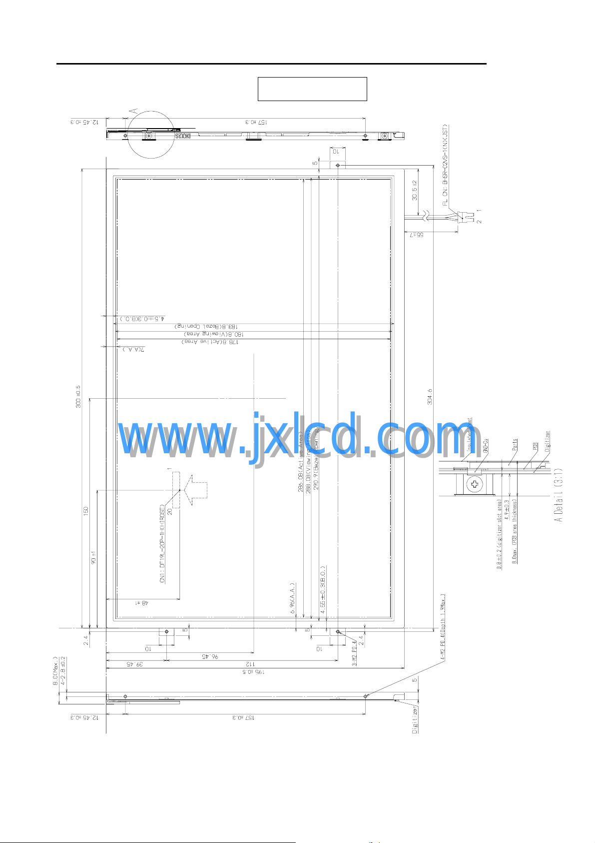
LTD133KX2S
DIMENSIONAL OUTLINE
(Front side)
Note) If customer remove tape for fixing FL cable, Toshiba Matsushita Display Technology can not
guarantee.
www.jxlcd.com
www.jxlcd.com
TENTATIVE
Unit : mm
Standard tolerance : ±0.5
(2/9) 2005-07-21 (Ver.0.4)
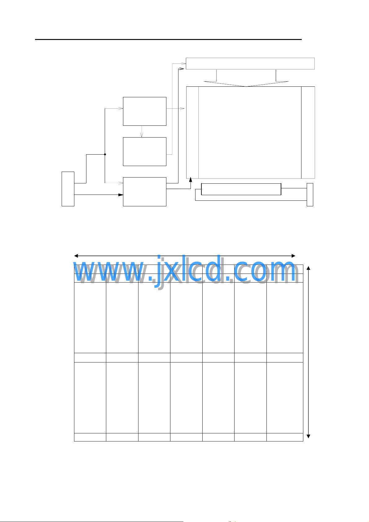
BLOCK DIAGRAM
CN1
Connector
1, 1 2, 1 X, 1 1280, 1
1, 2
www.jxlcd.com
www.jxlcd.com
DC/DC
converter
Gray scale
Manipulation
Voltage
Generation
Circuit
Panel
Controller
LVDS
1280 pixels
Gate driver
LTD133KX2S
Source driver
Liquid Crystal Panel
1280 x 800 pixels
Gate driver
Backlight
CN1
1, Y X, Y
1, 800 1280,800
(3/9) 2005-07-21 (Ver.0.4)
800 pixels
 Loading...