

Page 1
Product Information
Issued Date : July 27, 2005
SAMSUNG TFT-LCD
MODEL NO.:LTA460WS-L03
Note :
Any Modification of Spec is not allowed without SEC's permission.
Senior Engineer :
PREPARED BY :
LCD Application Engineering 3, TCS Team
Samsung Electronics Co . , LTD.
Doc . No LTA460WS-L03 Rev. No. 01-000-G-050727 Page 1 / 28
Page 2
Product Information
Contents
Revision History ----------------------------------------------------------------------- (3)
General Description ------------------------------------------------------------------- (4)
1. Absolute Maximum Ratings ------------------------------------------------------- (5)
1.1 Absolute Ratings Of Environment
1.2 Electrical Absolute Ratings
2. Optical Characteristics -------------------------------------------------------------- (7)
3. Electrical Characteristics ---------------------------------------------------------- (10)
3.1 TFT LCD Module
3.2 Back-light Unit
3.3 Inverter Input Condition & Specification
4. Block Diagram --------------------------------------------------------------------- (14)
4.1 TFT LCD Module
5. Input Terminal Pin Assignment -------------------------------------------------- (15)
5.1 Input Signal & Power
5.2 Inverter Input Pin Configuration
5.3 Inverter Input Power Sequence
5.4 LVDS Interface
5.5 Input Signals, Basic Display Colors and Gray Scale of Each Color
6. Interface Timing ------------------------------------------------------------------ (19)
6.1 Timing Parameters (DE only mode)
6.2 Timing Diagrams of interface Signal (DE only mode)
6.3 Power ON/OFF Sequence
7. Outline Dimension ---------------------------------------------------------------- (22)
8. Packing ---------------------------------------------------------------------------- (24)
9. Marking & Others ----------------------------------------------------------------- (25)
10. General Precautions ------------------------------------------------------------- (26)
Doc . No LTA460WS-L03 Rev. No. 01-000-G-050727 Page 2 / 28
Page 3
Revision History
Product Information
Date
July.27, 2005 000 All LTA460WS-L03 Model spec was issued first.
Revision
No.
Page Summary
Doc . No LTA460WS-L03 Rev. No. 01-000-G-050727 Page 3 / 28
Page 4
Product Information
General Description
*Description
LTA460WS-L03 is a color active matrix TFT (Thin Film Transistor) liquid crystal display
(LCD) that uses amorphous silicon TFTs as a switching devices. This model is composed
of a TFT LCD panel, a driver circuit and a back-light system. The resolution of a 46.0"
contains 1366 x 768 pixels and can display up to 16.7 million colors with wide viewing
angle of 89° or higher in all directions.
*Features
- High contrast ratio, high aperture structure
- SPVA(Super Patterned Vertical Align) mode
- Wide viewing angle(±178°)
- High speed response
- WXGA (1366 x 768 pixels) resolution (16:9)
- Low Power consumption
- Direct Type 24 CCFTs(Cold Cathode Fluorescent Tube)
- LVDS (Low Voltage Differential Signal) interface. (1pixel/clock)
* Applications
Home-alone Multimedia TFT-LCD TV
Display terminals for AV application products
High Definition TV (HDTV)
* General information
Items Specification Unit Note
Display area 1018.353(H) × 572.544(V) mm -
Driver element a-Si TFT active matrix -
Display colors 16.7M(8bits-true) colors -
Number of pixels 1366 x 768 pixel 16:9
Pixel pitch 0.7455(H) × 0.7455(V) mm
Display mode Normally Black -
R,G,B Vertical Strip =
0.2485(H)
Surface
treatment
Haze 41%, Hard Coating(3H) Conductive pol
Doc . No LTA460WS-L03 Rev. No. 01-000-G-050727 Page 4 / 28
Page 5
* Mechanical information
Item Min. Typ. Max. Note
Product Information
Module
Horizontal(H) - 1083.0 1084.0 mm
size
Vertical(V) - 627.0 628.0 mm
Depth(D) - 56.5 57.5 mm
Weight - 17,500 18,500 g
1. Absolute Maximum Ratings
1.1 Absolute ratings of environment
Item Symbol Min. Max. Unit Note
Storage temperature
Operating temperature
T
T
STG
OPR
-20 60
050
Shock ( non - operating ) Snop - 50 G (2),(4)
Vibration ( Non - operating ) Vnop - 1.5 G (3),(4)
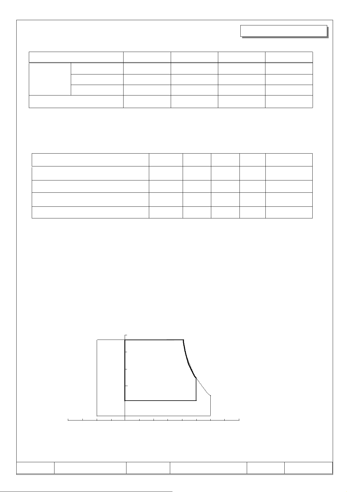
Note (1) Temperature and relative humidity range are shown in the figure below.
93.8 % RH Max. ( 40 °C≥Ta )
Maximum wet-bulb temperature at 39 °C or less.
(Ta > 40 °C) No condensation.
(2) 11ms, sine wave, 1 time for ±X, ±Y, ±Z axis
℃
℃
(1)
(1)
(3) 10∼300Hz/1.5G (10min/cycle, 30min for X,Y,Z axis)
(4) At testing Vibration and Shock, the fixture in holding the Module to be
tested have to be hard and rigid enough so that the Module would not
be twisted or bent by the fixture.
Relative Humidity(%RH)
100
80
60
40
20
90
Operating Range
(40, 90)
(50, 50.4)
(60, 27.7)
Storage Range
5
0
-20-40
0 20 40 60
80
Temperature(℃)
Doc . No LTA460WS-L03 Rev. No. 01-000-G-050727 Page 5 / 28
Page 6
Product Information
1.2 ELECTRICAL ABSOLUTE RATINGS
(1) TFT LCD MODULE (Vss = GND = 0 V)
Item Symbol Min. Max. Unit Note
Power
Supply
Voltage
NOTE (1) Within Ta ( 25 ± 2 °C)
LCD Module VDD Vss-0.5 5.5 V
Inverter V
CC
(1)
TBD TBD V
Doc . No LTA460WS-L03 Rev. No. 01-000-G-050727 Page 6 / 28
Page 7
Product Information
2. Optical Characteristics
The following items are measured under stable conditions. The optical characteristics
should be measured in a dark room or equivalent state with the methods shown in
Note (1).
◆
Measuring equipment : SR-3, BM-7
*Ta=25±2°C,V
Item Symbol Condition Min. Typ. Max. Unit Note
DD = 5V, fv = 60Hz, fDCLK =80MHz,IL=6.0mA
Contrast Ratio
(Center of screen)
Response
Time
Luminance of White
(Center of screen)
Color
Chromaticity
(CIE 1931)
Color Temperature k - 10000 -
Color Gamut - - 72 - %
Rising Tr - 10 13
Falling Tf - 6 7
Red
Green
Blue
White
C/R
YL 400 500 - cd/m
Rx
Ry 0.333
Gx 0.271
Gy 0.592
Bx 0.141
By 0.066
Wx 0.280
Wy 0.290
Normal
L,R=0
θ
U,D=0
θ
Viewing
Angle
800 1000 -
0.648
TYP.
-0.03
+0.03
TYP.
msec
(3)
SR-3
(4),(9)
BM-7
(5)
2
SR-3
(6)
SR-3
L
Hor.
Viewing
Angle
Ver.
Brightness
Uniformity
(9 points)
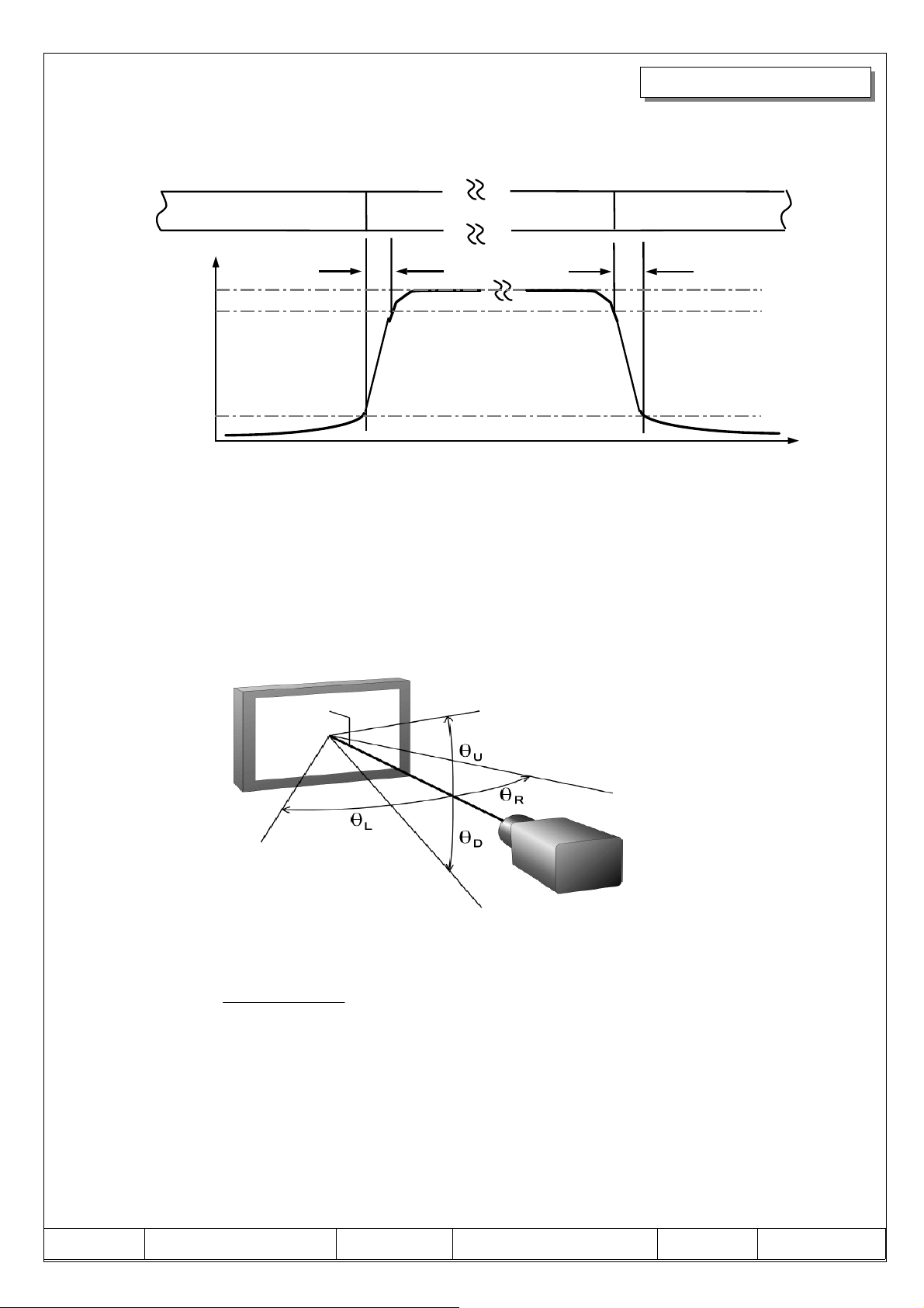
Note 1) Test Equipment Setup
The measurement should be executed in a stable, windless and dark room
between 30min and 40min after lighting the back-light at the given temperature
for stabilization of the back-light. This should be measured in the center of screen.
Asinglelampcurrent:6.0mA
Environment condition : Ta = 25 ± 2 °C
θ
θR
C/R≥10
U
θ
D
θ
Buni - - 25 %
75 89 75 89 75 89 75 89 -
Degrees
(7)
SR-3
(8)
SR-3
Doc . No LTA460WS-L03 Rev. No. 01-000-G-050727 Page 7 / 28
Page 8
Photo detector
Photo
detector Field
Product Information
SR-3 1°
BM-7 2°
TFT - LCD Module
Note 2) Definition of test point
Field
The center of the screen
Optical Measuring Equipment Setup
SR-3 : 50
BM-7 : 50
LCD Panel
㎝
㎝
228 683 1138
⑦
Active Area
Test Point
④
①
G
G
⑨
⑥
③
max
min
128
384
640
Note 3) Definition of Contrast Ratio (C/R) : Ratio of gray max ( Gmax) & gray min
(Gmin) at the center point(5) of the panel
CR
=
⑧
⑤
②
Gmax : Luminance with all pixels white
Gmin : Luminance with all pixels black
Doc . No LTA460WS-L03 Rev. No. 01-000-G-050727 Page 8 / 28
Page 9
Note 4) Definition of Response time : Sum of TR ,TF
−
Product Information
Display
Data
Optical
Response
Note 5) Definition of Luminance of White : Luminance of white at center point(5).
Note 6) Definition of Color Chromaticity (CIE 1931)
Color coordinate of Red , Green , Blue & White at center point(5).
Note 7) Definition of Viewing Angle : Viewing angle range (CR≥10 )
Black(TFT OFF)
100%
90%
10%
0%
R T
T
Black(TFT OFF)White(TFT ON)
F
Note 8) Definition of 9 points brightness uniformity
BB
Buni
=∗
Bmax : Maximum brightness
Bmin : Minimum brightness
(max min)
100
B
max
Doc . No LTA460WS-L03 Rev. No. 01-000-G-050727 Page 9 / 28
Page 10

Product Information
3. Electrical Characteristics
3.1 TFT LCD MODULE Ta = 25
Item Symbol Min. Typ. Max. Unit Note
C
°
Voltage of Power Supply
(a)Black
V
DD
4.5 5.0 5.5 V (1)
-1750- mA
Power
Consumption
I
DD
(2),(3)(b)White - 2000 - mA
(c)N-Pattern - 2300 2600 mA
Vsync Frequency
Hsync Frequency
Main Frequency
Rush Current
f
DCLK
RUSH
I
f
V
H
f
-60- Hz
46.3 50.18 - kHz
65 80 90 MHz
-4.56 A (4)
Note (1) Main pixel clock frequency is the value which is measured at the input of
LVDS transmitter.
(2) f
V=60Hz, fDCLK =80MHz, VDD = 5.0V, DC Current.
(3) Power dissipation check pattern(LCD Module only)
(a) Black Pattern (b) White Pattern
(C) N-pattern
Doc . No LTA460WS-L03 Rev. No. 01-000-G-050727 Page 10 / 28
Page 11

(4) Measurement Conditions
Product Information
CONTROL SIGNAL
(HIGH to LOW)
12V
5V
C3
1uF
R1
47K
R2
1K
R3
47K
M1
2SK1059
M2
2SK1399
C2
10000pF
Note : Control Signal : High(+5V) -->Low(Ground)
All Signal lines to panel except for power 5V : Ground
The rising time of supplied voltage is controlled to 470us by R and C value.
VDD rising time is 470us
DD rising time is 470us
V
FUSE
VDD ( LCD INPUT)
C1
1uF
GND
GND
0.1VDD
0.1VDD
0.9VDD
0.9VDD
470us
470us
3.3V
3.3V
Doc . No LTA460WS-L03 Rev. No. 01-000-G-050727 Page 11 / 28
Page 12
Product Information
3.2 BACK-LIGHT UNIT
The back-light system contains 24 direct-lighting type CCFTs (Cold Cathode Fluorescent
Tube). Life time (Hr) of a lamp, 50,000 hours, is defined as the time in which it
continues to operate under the condition of Ta = 25±2°C and typical luminance for a
lamp until the brightness becomes 50% or lower than it's original value.
Parameter SYMBOL MIN. TYP. MAX. UNIT NOTE
Lamp Current I
Lamp Voltage V
Lamp Frequency f
L 4.0 6.0 7.0
L 1480 1540 1600 Vrms (1)
L 40 - 80
㎃
rms (1)
㎑
(2)
Operating Life Time Hr 50,000 - - Hour (3)
0℃:2500
Start Up Voltage Vs - -
Vrms (4)
25℃:1990
Note) The waveform of the inverter output voltage must be area symmetric
and the design of the inverter must have specifications for the
modularized lamp. Specified values are for a single lamp.
The performance of the back-light, for example life time or brightness, is much
influenced by the characteristics of the DC-AC inverter for the lamp. So all the
parameters of an inverter should be carefully designed so as not to produce too much
leakage current from high-voltage output of the inverter.
When you design or order the inverter, please make sure that a poor lighting caused
by the mismatch of the back-light and the inverter(miss lighting, flicker, etc.) never
occur. When you confirm it, the module should be operated in the same condition as
it is installed in your instrument.
Note (1) lamp current is measured with current meter.
Refer to the following block diagram of the back-light unit for more information.
HOT1
HOT2
Inverter
Inverter
HOT1
HOT2
LCD
Module
HOT23
HOT24
HOT23
HOT24
Doc . No LTA460WS-L03 Rev. No. 01-000-G-050727 Page 12 / 28
Page 13

Product Information
(2) Lamp frequency may produce interference with horizontal synchronous
frequency and this may cause line flow on the display. Therefore We
synchronized the lamp frequency to horizontal frequency.
(3) Life time (Hr) of a lamp is defined as the time in which it continues to operate
under the condition of Ta = 25±2°C and IL = 7.0 mArms(max) for a lamp until
the brightness becomes 50% or lower than it's original value.
(4) If an inverter has shutdown function it should keep its output for more than 1
second even if the lamp connector open. Otherwise the lamps may not to be
turned on.
3.3 Inverter Input Condition & Specification
Specifications
Items Symbol Conditions
Min. Typ. Max.
Unit Note
Input
Voltage
Input
Current
Lamp
Current
Frequency FL
Backlight
On/Off
Dimming
Control
Vin - 23 24 25 V Ta=25
Iin
Io,max Vdim=3.3 V 5.5 6.0 6.5 mArms
Io,min Vdim= 0 V 25 30 35 %
ON Vin=24 2.4 - 5.25
OFF Vin=24 0 - 0.8
Max
Lum
Min.
Lum
Vin=24.0V,
Vdim=3.3 V
Vin=24 V
Adim=3.3V
Vdim - 3.3 -
Vdim - 0 -
8.19 9.1 10.01 Adc
55 60 65 kHz
℃
After 120 min
Warm-up
@Vin=24V
(1)
V
V DC input
Note (1) Power Consumption is measured when 500[cd/m2] of luminance which is
the typ. luminance. Max Value of the Power Consumption is measured at
initial turn on of the backlight.
Doc . No LTA460WS-L03 Rev. No. 01-000-G-050727 Page 13 / 28
Page 14

4. Block Diagram
4.1 TFT LCD MODULE
CONNECTOR
CONNECTOR
LVDS 1ch
LVDS 1ch
MAIN POWER
MAIN POWER
Timing
Timing
Timing
Timing
Controller
Controller
Controller
Controller
( MERGED
( MERGED
( MERGED
( MERGED
LVDS )
LVDS )
LVDS )
LVDS )
MEMORY
MEMORY
RSDS Si g nal
RSDS Si g nal
CPV,OE,STV
CPV,OE,STV
CPV,OE,STV
CPV,OE,STV
Terminat ion Resistor
Terminat ion Resistor
SOU R C E DRIVE IC
SOU R C E DRIVE IC
SOU R C E DRIVE IC
SOU R C E DRIVE IC
(S6C2101,384CH)
(S6C2104,414CH)
(S6C2101,384CH)
(S6C2104,414CH)
Control Signal (TP, POL, STH)
Control Signal (TP, POL, STH)
Control Signal (TP, POL, STH)
Control Signal (TP, POL, STH)
GATE DRIVE IC
GATE DRIVE IC
GATE DRIVE IC
GATE DRIVE IC
(KS0655, 128CH )
(KS0655, 128CH )
( 256CH)
( 256CH)
x 6 EA
x 6 EA
x 3 EA x 2 B ank
x 3 EA x 2 B ank
x 10 EA
x 10 EA
x 10 EA
x 10 EA
Product Information
VON,VOFF,DVDD
VON,VOFF,DVDD
VON,VOFF,DVDD
(5V)
(5V)
DC-DC BLOCK
DC-DC BLOCK
DC-DC BLOCK
DC-DC BLOCK
& Gamma Gene ra t i o n
& Gamma Gene ra t i o n
& Gamma Gene ra t i o n
& Gamma Gene ra t i o n
VON,VOFF,DVDD
Doc . No LTA460WS-L03 Rev. No. 0.0-050727 Page 14 / 28
Page 15

5. Input Terminal Pin Assignment
5.1. Input Signal & Power : Connector FI-E30S (JAE)
No. Signal No. Signal
1 Do not connect* 16 GND
2 Do not connect* 17 Rx33 Do not connect* 18 Rx3+
4GND19GND
5Rx0-20Do not connect*
6Rx0+21LVDS OPTION **
7GND22Do not connect*
8Rx1-23GND
9Rx1+24 GND
10 GND 25 GND
Product Information
11 Rx2- 26 V
12 Rx2+ 27 V
13 GND 28 V
14 RxCLK- 29 V
15 RxCLK+ 30 V
* NOT CONNECTED : THIS PINS ARE ONLY USED FOR SEC INTERNAL OPERATIONS.
** LVDS OPTION : IF THIS PIN : HIGH (3.3 V)
OTHERWISE : LOW (GND) OR OPEN(NC)
*** Sequence : On = Vdd(T1)≥LVDS Option≥Interface Signal(T2)
OFF = Interface Signal(T3)≥LVDS Option≥Vdd
→
NORMAL NS LVDS FORMAT
DD (+5V DC)
DD (+5V DC)
DD (+5V DC)
DD (+5V DC)
DD (+5V DC)
→
JEIDA LVDS FORMAT
Doc . No LTA460WS-L03 Rev. No. 01-000-G-050727 Page 15 / 28
Page 16

5.2. Inverter Input Pin Configuration
Pin No. Pin Configuration(FUNCTION)
124V
224V
324V
424V
524V
6GND
7GND
8GND
9GND
10 GND
11 ERROR DETECTION (NORMAL : GND / ABNORMAL : FLOATING)
12 Backlight On /Off
13 Analog Dimming Control
Product Information
Connector : S14B-PH-SM3-TB(JST)
14 Do not connect*
5.3 Inverter Input Power Sequence
Vin (24V)
Dimming Control
(0 ~ 3.3V)
0.5sec[Min]
Backlight On/Off
1.1sec [Min]
0.5sec [Min]
0.5sec [Min]
0.1sec [Min]
Doc . No LTA460WS-L03 Rev. No. 01-000-G-050727 Page 16 / 28
Page 17

5.4 LVDS Interface
-LVDSReceiver:Tcon(merged)
- JEIDA & Normal Data Format
Product Information
LVDS pin JEIDA -DATA VESA -DATA
TxIN/RxOUT0 R2 R0
TxIN/RxOUT1 R3 R1
TxIN/RxOUT2 R4 R2
TxOUT/RxIN0
TxOUT/RxIN1
TxIN/RxOUT3 R5 R3
TxIN/RxOUT4 R6 R4
TxIN/RxOUT6 R7 R5
TxIN/RxOUT7 G2 G0
TxIN/RxOUT8 G3 G1
TxIN/RxOUT9 G4 G2
TxIN/RxOUT12 G5 G3
TxIN/RxOUT13 G6 G4
TxIN/RxOUT14 G7 G5
TxIN/RxOUT15 B2 B0
TxIN/RxOUT18 B3 B1
TxIN/RxOUT19 B4 B2
TxIN/RxOUT20 B5 B3
TxIN/RxOUT21 B6 B4
TxOUT/RxIN2
TxOUT/RxIN3
TxIN/RxOUT22 B7 B5
TxIN/RxOUT24 HSYNC HSYNC
TxIN/RxOUT25 VSYNC VSYNC
TxIN/RxOUT26 DEN DEN
TxIN/RxOUT27 R0 R6
TxIN/RxOUT5 R1 R7
TxIN/RxOUT10 G0 G6
TxIN/RxOUT11 G1 G7
TxIN/RxOUT16 B0 B6
TxIN/RxOUT17 B1 B7
TxIN/RxOUT23 RESERVED RESERVED
Doc . No LTA460WS-L03 Rev. No. 01-000-G-050727 Page 17 / 28
Page 18

Product Information
5.5 Input Signal, Basic Display Colors and Gray Scale of Each Color
DATA SIGNAL GRAY
COLOR DISPLAY
BLACK 0 0 0 0 0 0 0 0 0 0 0 0 0 0 0 0 0 0 0 0 0 0 0 0 -
BLUE 0 0 0 0 0 0 0 0 0 0 0 0 0 0 0 0 1 1 1 1 1 1 1 1 -
GREEN 0 0 0 0 0 0 0 0 1 1 1 1 1 1 1 1 0 0 0 0 0 0 0 0 BASIC
COLOR
GRAY
SCALE
OF
RED
GRAY
SCALE
OF
GREEN
GRAY
SCALE
OF
BLUE
CYAN 0 0 0 0 0 0 0 0 1 1 1 1 1 1 1 1 1 1 1 1 1 1 1 1 -
RED 1 1 1 1 1 1 1 1 0 0 0 0 0 0 0 0 0 0 0 0 0 0 0 0 -
MAGENTA 1 1 1 1 1 1 1 1 0 0 0 0 0 0 0 0 1 1 1 1 1 1 1 1 -
YELLOW 1 1 1 1 1 1 1 1 1 1 1 1 1 1 1 1 0 0 0 0 0 0 0 0 -
WHITE 1 1 1 1 1 1 1 1 1 1 1 1 1 1 1 1 1 1 1 1 1 1 1 1 -
BLACK 0 0 0 0 0 0 0 0 0 0 0 0 0 0 0 0 0 0 0 0 0 0 0 0 R0
DARK
↑
↓
LIGHT
RED 1 1 1 1 1 1 1 1 0 0 0 0 0 0 0 0 0 0 0 0 0 0 0 0 R255
BLACK 0 0 0 0 0 0 0 0 0 0 0 0 0 0 0 0 0 0 0 0 0 0 0 0 G0
DARK
↑
↓
LIGHT
GREEN 0 0 0 0 0 0 0 0 1 1 1 1 1 1 1 1 0 0 0 0 0 0 0 0 G255
BLACK 0 0 0 0 0 0 0 0 0 0 0 0 0 0 0 0 0 0 0 0 0 0 0 0 B0
DARK
↑
↓
LIGHT
BLUE 0 0 0 0 0 0 0 0 0 0 0 0 0 0 0 0 1 1 1 1 1 1 1 1 B255
R0 R1 R2 R3 R4 R5 R6 R7 G0 G1 G2 G3 G4 G5 G6 G7 B0 B1 B2 B3 B4 B5 B6 B7
1 0 0 0 0 0 0 0 0 0 0 0 0 0 0 0 0 0 0 0 0 0 0 0 R1
0 1 0 0 0 0 0 0 0 0 0 0 0 0 0 0 0 0 0 0 0 0 0 0 R2
: : : : : : : : : : : : : : : : : : : : : : : :
: : : : : : : : : : : : : : : : : : : : : : : :
1 0 1 1 1 1 1 1 0 0 0 0 0 0 0 0 0 0 0 0 0 0 0 0 R253
0 1 1 1 1 1 1 1 0 0 0 0 0 0 0 0 0 0 0 0 0 0 0 0 R254
0 0 0 0 0 0 0 0 1 0 0 0 0 0 0 0 0 0 0 0 0 0 0 0 G1
0 0 0 0 0 0 0 0 0 1 0 0 0 0 0 0 0 0 0 0 0 0 0 0 G2
: : : : : : : : : : : : : : : : : : : : : : : :
: : : : : : : : : : : : : : : : : : : : : : : :
0 0 0 0 0 0 0 0 1 0 1 1 1 1 1 1 0 0 0 0 0 0 0 0 G253
0 0 0 0 0 0 0 0 0 1 1 1 1 1 1 1 0 0 0 0 0 0 0 0 G254
0 0 0 0 0 0 0 0 0 0 0 0 0 0 0 0 1 0 0 0 0 0 0 0 B1
0 0 0 0 0 0 0 0 0 0 0 0 0 0 0 0 0 1 0 0 0 0 0 0 B2
: : : : : : : : : : : : : : : : : : : : : : : :
: : : : : : : : : : : : : : : : : : : : : : : :
0 0 0 0 0 0 0 0 0 0 0 0 0 0 0 0 1 0 1 1 1 1 1 1 B253
0 0 0 0 0 0 0 0 0 0 0 0 0 0 0 0 0 1 1 1 1 1 1 1 B254
RED GREEN BLUE
SCALE
LEVEL
R3~R252
G3~G252
B3~B252
Note) Definition of Gray :
Rn : Red Gray, Gn : Green Gray, Bn : Blue Gray (n = Gray level)
Input Signal : 0 = Low level voltage, 1 = High level voltage
Doc . No LTA460WS-L03 Rev. No. 01-000-G-050727 Page 18 / 28
Page 19

6. Interface Timing
6.1 Timing Parameters ( DE only mode )
SIGNAL ITEM SYMBOL MIN. TYP. MAX. UNIT NOTE
Product Information
Clock
Hsync Fh 46.3 50.18 - KHz Vsync Fv - 60 - Hz -
Vertical
Active
Disply Term
Horizontal
Active
Display Term
Note) This product is DE only mode. The input of Hsync & Vsync signal does
not have an effect on normal operation.
Frequency
Display
Period
Vertical
Total
Display
Period
Horizontal
Total
1/T
C 65 80 90 MHz -
TVD - 768 - lines -
TVB 773 838 - lines -
THD - 1366 - clocks -
TH 1570 1600 1700 clocks -
Doc . No LTA460WS-L03 Rev. No. 01-000-G-050727 Page 19 / 28
Page 20

6.2 Timing diagrams of interface signal ( DE only mode )
T
V
T
VB
T
C
DE
DE
D
CLK
T
VD
T
H
T
HD
Product Information
DATA
SIGNALS
D
CLK
DISPLAY
DATA
T
C
T
CH
T
DS
T
ES
T
CL
0.5 V
CC
T
DH
0.5 V
CC
DE
0.5 V
CC
Doc . No LTA460WS-L03 Rev. No. 01-000-G-050727 Page 20 / 28
Page 21

Product Information
6.3 Power ON/OFF Sequence
: To prevent a latch-up or DC operation of the LCD module, the power on/off
sequence should be as the diagram below.
Power
Supply V
Vss
DD
0.1V
DD
Interface Signal
with Data Enable
Vss
Power Supply
For B/L unit
T
1
0.9V
0.9V
T
DD
2
DD
T
0.1V
DD
T
4
3
VALID
T
6
Power OFF
Power ON
T
5
0.5Vcc 0.5Vcc
0<T1≤10msec
0<T2≤50msec
0<T3≤50msec
1sec≤T4
1000 msec≤T5 ( Recommend Value)
100 msec≤T6 (Recommend Value)
NOTE.
(1) The supply voltage of the external system for the module input should be the
same as the definition of VDD.
(2) Apply the lamp voltage within the LCD operation range. When the back-light
turns on before the LCD operation or the LCD turns off before the back-light
trns off, the display may momentarily become abnormal screen.
(3) In case of VDD = off level, please keep the level of input signals on the low
or keep a high impedance.
(4) T4 should be measured after the module has been fully discharged between
power off and on period.
(5) Interface signal shall not be kept at high impedance when the power is on.
Doc . No LTA460WS-L03 Rev. No. 01-000-G-050727 Page 21 / 28
Page 22

Page 23

Page 24

8. PACKING
8.1 Carton
1) Packing Form
CorrugatedfiberboardboxandEPScushionasshockabsorber
2) Packing Method
Packing
-Pallet box
Cushion-Foam
Product Information
→
Directionbeabletoopenit
LCD Module
Cushion-Foam
Pallet-Plastic
8.2 Packing Specification
ITEM Specification Remark
LCD Packing
(Packing-Pallet Box)
1Box / Pallet
Pallet-Plastic
(PE,W1150,L985,H125,
Packing
Direction
10ea / Box
BLUE)
Vertical -
1. 160 Kg / LCD (10ea)
2. 10 Kg / Cushion-Foam (2ea)
3. 8 Kg / Packing-Pallet Box (1ea)
4. Cushion-Foam Material : EPS
5. Packing-Pallet Box Material : DW4
1. Pallet weight = 8.8kg
2. 8.8 Kg / Pallet
Pallet size H x V x height
Pallet weight 187kg
1270mm(H) x 1150mm(V) x
844mm(height)
Pallet (8.8kg) + Cushion-Foam (10kg)
+Module(160kg)+Packing-PalletBox
(8kg)
Doc . No LTA460WS-L03 Rev. No. 01-000-G-050727 Page 24 / 28
Page 25

MARKING & OTHERS
10.
A nameplate bearing followed by is affixed to a shipped product at the
specified location on each product.
Product Information
(1) Parts number : LTA460WS-L03-00R7
1 2 345 6 78 9
(2) Lot number : 7 I 5 F 020 79 E
12345 6 7
①
7:Line
②
I:Device
③
5:Year
④
F : Month
⑤
020 : LOT No.
⑥
79 : GLASS No.
⑦
E : CELL No.
(3) Nameplate Indication
LTA460WS-L03
①
LTA : AV model
②
460 : Panel Size
③
W:WXGA
④
S : Generation
⑤
L:LVDS
⑥
03 : Derivation No.
⑦
0 : Customer Code
⑧
0R : Revision No.
⑨
7:Line
0504
MADE IN KOREA
(4) Packing Pallet Label
DEVICE : LTA460WS-L03
TYPE :
QUANTITY : 10 PCS
MADEIN KOREA
ZAT5040001
1234 5 6
7I5F02079E
ZAT5040001
①
Z:PALLET
②
A:LINE
③
T : CITE CODE
④
5:YEAR
⑤
04 : WEEK
⑥
0001 : SERIAL N o.
Doc . No LTA460WS-L03 Rev. No. 01-000-G-050727 Page 25 / 28
Page 26

Product Information
10. General Precautions
10.1 Handling
(a) When the module is assembled into a system, it should be attached firmly
using all mounting holes. Be careful not to twist and bend the modules.
(b) Refrain from strong mechanical shock and / or any force to the module. In
addition to damage, this may cause improper operation or damage to the
module and CCFL back-light.
(c) Note that polarizers are very fragile and can be easily damaged. Do not press
or scratch the surface harder than a HB pencil lead.
(d) Wipe off water droplets or oil immediately. If you leave the droplets for a
long time, Staining and discoloration may occur.
(e) If the surface of the polarizer is dirty, clean it using absorbent cotton or soft
cloth.
(f) The desirable cleaners are water, IPA(Isopropyl Alcohol) or Hexane. Do not use
Ketone type materials (ex. Acetone), Ethyl alcohol, Toluene, Ethyl acid or Methyl
chloride. It may cause permanent polarizer damage due to the chemical reaction.
(g) If the liquid crystal material leaks from the panel, it should be kept away
from the eyes and mouth. In case of contact with skin or clothes, thoroughly
wash it away with soap and water.
(h) Protect the module from static electricity. It may cause damage to the C-MOS
Gate Array IC.
(i) Use finger-stalls with soft gloves to keep display clean during the incoming
inspection and the assembly process.
(j) Do not disassemble the module.
(k) Do not pull or fold the lamp wire.
(l) Do not adjust the variable resistor located on the back side.
(m) I/F connector pins should not be touched directly with bare hands.
Doc . No LTA460WS-L03 Rev. No. 01-000-G-050727 Page 26 / 28
Page 27

Product Information
10.2 Storage
(a) Do not expose the module in high temperature, and/or high humidity for a long
time. It is highly recommended to store the module within the temperature
from 0 to 35°C and relative humidity of less than 70%.
(b) Do not store the TFT-LCD module in direct sunlight. The module shall be stored
in a dark place. Prolonged exposure to sunlight or fluorescent light during the
storagewilldamagethemodule.
10.3 Operation
(a) Do not connect or disconnect the module in the “Power On” condition.
(b) Power supply should always be turned on/off by following item 6.3
" Power on/off sequence ".
(c) The Module has high frequency circuits. Sufficient suppression to the
electromagnetic interference shall be done by system manufacturers.
Grounding and shielding methods may be important to minimize the
interference.
(d) The cable between the back-light connector and its inverter power supply
should be at the minimum length possible to be connected directly. The
longer cable between the back-light and the inverter may cause lower
luminance of lamp(CCFT) and may require higher startup voltage(Vs).
10.4 Operation Condition Guide
(a) The LCD product should be operated under normal conditions.
Normal condition is defined as below;
- Temperature : 20±15
- Humidity : 65±20%
- Display pattern : continually changing pattern (Not stationary)
(b) If the product will be used in extreme conditions such as high temperature,
humidity, display patterns or operation time etc.., It is strongly recommended
to contact SEC for Application engineering advice. Otherwise, its reliability and
function may not be guaranteed. Extreme conditions are commonly found at
Airports, Transit Stations, Banks, Stock market, and Controlling systems.
℃
Doc . No LTA460WS-L03 Rev. No. 01-000-G-050727 Page 27 / 28
Page 28

Product Information
10.5 Others
(a) Use Ultra-violet light filters if outdoor operation is necessary.
(b) Avoid water condensation. Moisture may penetrate sensitive electrical
connections resulting in improper operation.
(c) Do not exceed the absolute maximum rating values. (supply voltage
variation, input voltage variation, variation in part contents and environmental
temperature, etc..) Otherwise, the module may be damaged.
(d) If the module displays the same pattern continuously for a long period of
time, it can result in the situation where the image “sticks” (remains) on the
screen. We recommend that you should discuss SEC when you want the
module to be operated in displaying the same pattern for a long time.
(e) The module has sensitive PCB circuitry on the back side and should be
handled carefully in order prevent stress and possible failure.
Doc . No LTA460WS-L03 Rev. No. 01-000-G-050727 Page 28 / 28
 Loading...