

Page 1

製品標準
( LTA460HQ18-C )
1/37
Page 2
1. 목적
제품 정보를 정의하고 개발제품 Target을 설정하며, 이를 부서간에 공유하기 위함.
2. 적용범위
TFT LCD LTA460HQ18-C01
3. 일반개요
3.1 개요
LTA460HQ18-C01는 비정질 실리콘(Amorphous Silicon) 박막 트랜지스터(TFT; Thin Film
Transistor)를 스위칭 소자로 사용한 컬러 능동 행렬(Color active matrix) 방식의 TFT 액정 표
시소자(LCD;Liquid Crystal Display) Module이다.
Module은 Panel, 구동 회로부와 Backlight부로 구성되며, Interface 방법은 Digital 영상정보를
직렬로 고속 전송하는 방식의 일종인 LVDS방식을 채용하였다.
본 제품은 1,920 * 1,080(16:9) 화소를 포함하고, 1.07B (Dithered 10bit)의 색상을 지원한다.
그리고 독자 기술인 SVA Mode 기술을 적용하여 시야각은 상하좌우 89°이상을 제공하는 광시야각
제품이며, 고속 응답 속도를 지원하는 60Hz 지원 제품이다.
3.2 특징
① High Contrast Ratio & High aperture structure
②고속응답특성(DCC적용회로채용)
③ FHD (1,920 * 1080 화소) 지원 (16:9)
④ SVA (Super Vertical Align) Mode 광시야각(±178°)
⑤ Sync Format : DE(Data Enable) Mode 지원, H/V-sync 지원 불가
⑥ E-LED B/L Unit 설계 적용
2CH-LVDS 직렬 인터페이스( 2*1pixel/clock)
⑦
3.3 응용분야
① Public Display
② Home-alone Multimedia TFT-LCD TV
③ High Definition TV Ready (HD TV Ready)
④ AV 제품의 화상 표시 단말기
3.4 일반사양
항목 사양 단위 비고
유효표시면적 1018.08(H) x 572.67(V) ㎜
구동소자 a-Si TFT Active matrix
표현가능색 수 1.07B (Dithered 10bit) color
화소수 1,920 × 1,080 pixel 16 : 9
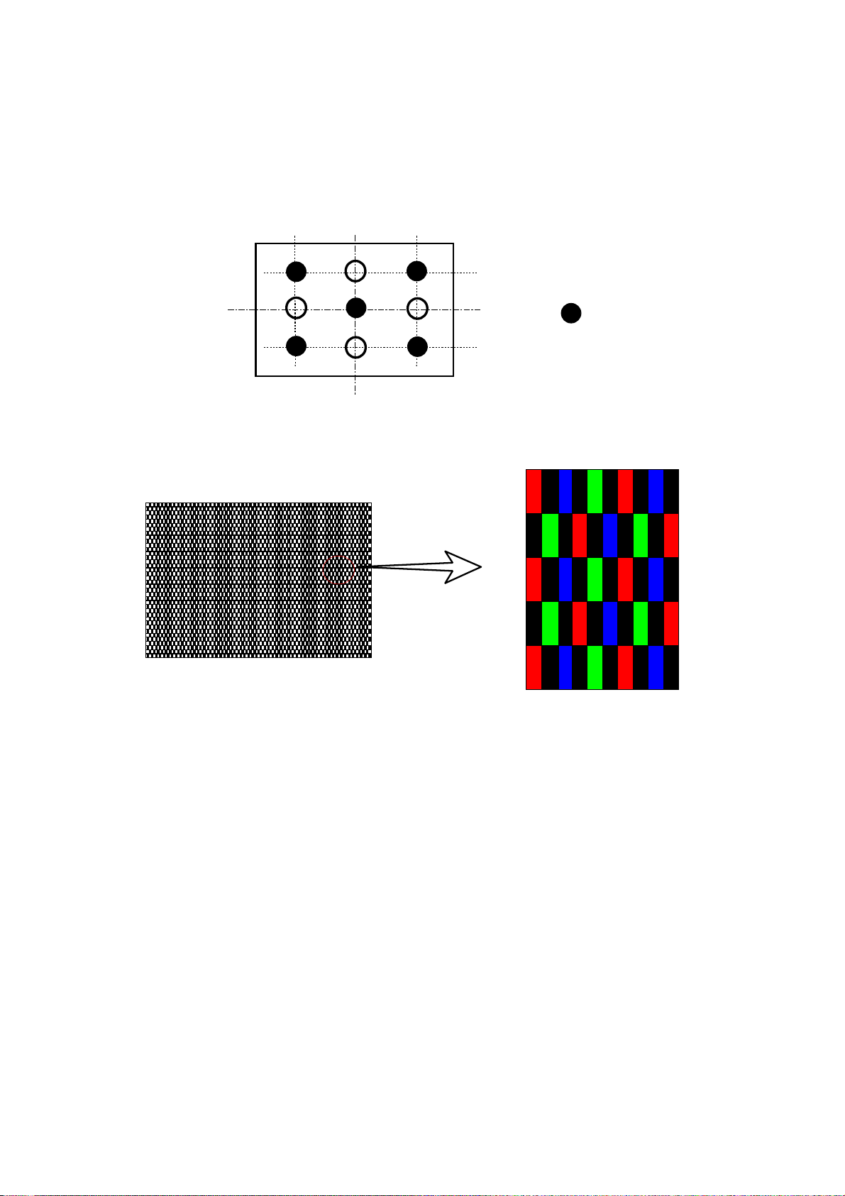
화소배열 RGB Vertical Stripe
화소크기 0.17675 (H) × 0.53025 (V) ㎜
표시모드 Normally Black
표면처리 S-POL, ANTI GLARE
2/38
Page 3
4. 기구사양
Item Min. Typ. Max. Note
Horizontal(H) 1044.9 1045.9 1046.9 mm
Module
size
5. 절대 최대 정격
5.1환경사양절대정격
Storage temperature TSTG -20 65 ℃ (1)
Operating temperature
(Ambient temperature)
Shock ( non - operating ) Snop
Vibration ( Non - operating ) Vnop - 1.5 G (3),(4)
Vertical(V) 601.1 602.1 603.1 mm
mm
Depth(D) 30.2 31.2 34.2
( With Converter )
Weight - 11.3 12.3 Kg
Item Symbol Min. Max. Unit Note
TOPR 0 50 ℃ (1)
x, y 축 - 40
G (2),(4)
z축 - 30
NOTE (1) 온도와 상대습도 관계는 아래 그림에 따른다.
(최대습구 온도는 39℃임 <40℃에서 93.8%RH에 해당>)
NOTE (2) 11ms, sine wave, 1 time for ±X, ±Y, ±Z axis
NOTE (3) 10-300 Hz, Sweep rate 10min, 30min for X,Y,Z axis
NOTE (4) 진동 및 충격 Test시 모듈을 고정하는 치구는 모듈이 치구에 의해 트위스트 되거나
Bent되지 않도록 충분히 견고해야 한다.
Relative Humidity ( %RH)
100
90
80
60
Operating Range
40
20
Storage Range
5
0
-40 -20 0 20 40 60
80
Temperature (
3/38
O
C)
Page 4
5.2 전기적 사양 절대 정격
5.2.1 TFT LCD MODULE 절대 정격 (VSS = 0 V)
ITEM SYMBOL MIN. MAX. UNIT NOTE
Power Supply Voltage / Analog VAVDD 10.8 13.2 V
(1)
Power Supply Voltage / Digital VDD VSS-0.3 13.2 V
NOTE(1) 동작온도 범위안에서.
5.2.2 BACK-LIGHT UNIT 절대정격 (Ta:25±2℃)
항 목 기호 SPEC. 단위 비고
입력 전압 V
IN
입 력 전 류 Iin 7.1 Adc MAX V
22 ~ 26 V 24V Typ.
=24V
IN
출력 전류(Max.) Io 280 mA MAX
사용 온도 범위 Top 0 ~+60 ℃
보존 온도 범위 Tstg -30 ~ +80 ℃
사용 상대 습도 RHop 90%RH % No wet condition
NOTE(1) 최대치를 초과할 경우, 영구적인 결함이 발생할 수 있음. 명시된 정상조건 내에서
구동되어야함.
5.2.3 LED UNIT Absolute Maximum Rating
항 목 기호 최대정격 단위 비고
Operating temperature range Top -20 ~ 70 ℃
Storage temperature range Tstg -30 ~ 85 ℃
Junction Temperature Tj 150 ℃
Forward current
Forward Voltage
Thermal resistance, Junction to PCB
If 260 ㎃ Continuous operation@string
Ifp 310 ㎃ Duty 50% operation@string
Vf 118 V
Vfp 121 V
Continuous operation@string
@260mA
Impulsive operation@string
@310mA
Rth,JS 20 K/W
4/38
Page 5
6. 광학 특성
6.1 측정 환경
-. 환경 조건
온도 : 25℃±2℃ / 습도 : 25%~85% RH / 압력 : 86kPa~106kPa / 암실 : 1Lux이하 /
무풍(직접적인 바람 제거) / 무진동
-. Warm-Up Time : ① 최소 30분 이상
②주기적(약15초간격)으로center휘도를측정하여10분전휘도와
현재 휘도 차이의 비가 0.5%이하가 되는 최초 시점
Twarm-up = (| Lumt-10 - Lumnow | / Lumnow ) × 100 < 0.5 가 되는 시간
where , Lum
는10분전휘도,Lum
t-10
는현재휘도
now
6.2 측정 장비(LMD : Light Measurement Device)
-. 종류 : BM-5A(TOPCON社), BM-7(TOPCON社), SR-3(TOPCON社), RD-80S(TOPCON社),
PR-650(Photo Reserch社), EZ-Contrast(Eldim社)
-.측정거리및방향:
6.3 구동 조건
-. TFT LCD Module:V
LCD
θ=90°± 0.3°
LMD
d= 50Cm
LMD Field
BM-5A / SR-3 2°
BM-7 / RD-80S 2°/ 1°
PR-650 1°
=12.0V,fV=120㎐, fDCLK = 297㎒, Column반전 구동
DD
5/38
Page 6
6.4
광학 특성
Item Symbol Condition Min. Typ. Max. Unit Note
Transmittance T 5.5 6.0 % (1)
Contrast Ratio
(Center of screen)
Response
Time
(Avg)
Luminance of White
(Center of screen)
Color
Green
Chromaticity
(CIE 1931)
White
GtoG
Red
Blue
C/R
3,000 4,000 -
- 6 18 msec
Normal
f=0
YL 350 400 - cd/m
Rx
Ry 0.330
q=0
0.650
Viewing
Angle
Gx 0.310
Gy 0.600
Bx 0.150
TYP.
-0.03
TYP.
+0.03
By 0.060
Wx 0.280
Wy 0.290
※0↔255G는
2
(2)
SR-3
(5)
BM-7
RD-80S
제외
(3)
SR-3
(4)
PR650,
SR-3
Center
Point
Color Reproducibility 70 % SR-3
Color Temperature CCT 7,000 10,000 13,000 K SR-3
Viewing
Angle
Hor.
Ver.
qL
q R 75 89 -
f H 75 89 -
C/R >
10 :1
75 89 -
Degrees
(6)
EZ-
Contrast
f L 75 89 -
Brightness Uniformity
(4)
Buni - - 25 %
(9 points)
SR-3
(8)
Flicker - - 20
BM-7
RD-80S
DSHA 101-255 - - 5.0 %
(7)
Crosstalk
DSHA 20-100 - - 15.0 %
BM-5A
DSHA 0 - 19 X(관리안함) %
Gamma Value 1.9 2.2 2.5
※ 측정 조건 : LCD Assy Module 조건에서 측정함
6/38
PI 기재
불가
Page 7
NOTE (1)
▶ 측정위치 : 판넬상 측정위치는 Active Area내 9개 점으로 한다.(하기의 그림 참조)
① TRANSMITTANCE 평균의 정의 (T
PANEL
-. 측정위치 중앙 Point⑤ 에서 TRANSMITTANCE (TPANEL)
-. 표준광원을 이용하여 PANEL 투과율 측정
NOTE (2) 대비비(C/R : Contrast ratio)
: 측정위치 중앙(Point ⑤)에서 White 상태(GMAX)와 Black 상태(GMIN)의 비로 정의.
판넬상에서
C/R =
판넬상에서
NOTE (3) White 휘도의 정의 (YL) :
측정위치 중앙(Point ⑤)의 white 휘도(YL) 를 측정한 값.
NOTE (4) Brightness Uniformity(Buni) :
측정 화면 : Fully White
측정화면상의 9개의 휘도를 측정, 아래와 같이 정의한다.
)
WHITE
BLACK
상태 휘도
상태 휘도
B B
max min
−
max
B
× 100
where, Bmax = Maximum brightness
Bmin = Minimum brightness
7/38
Page 8
NOTE (5)
▶ 응답시간(Response time)의 정의: 화면이 어두워 질 때와 밝아질 때에 투과율이 10%와 90%
사이로 변화하는 시간의 합
- Normally Black mode일 경우
Start
Tf
Black(TFT Off)
100%
90%
10%
0%
Black(TFT Off)
Tr
White(TFT On)
Time
Gray t o Gray Res ponse Time
Gray
0 31 63 95 127 159 191 223 255
0
31
Tf (31-0) T r (31-63) Tr ( 31-95) Tr ( 31-127) Tr ( 31-159) Tr ( 31-191) Tr (31-223) Tr (31-255)
63
Tf (63-0) T f (63-31) Tr (63-95) T r (63-127) T r (63-159) Tr ( 63-191) Tr (63-223) Tr (63-255)
95
Tf (95-0) T f (95-31) Tf (95-63) T r (95-127) Tr ( 95-159) Tr ( 95-191) Tr ( 95-223) Tr (95-255)
127
Tf (127-0) Tf (127-31) T f ( 127-63) Tf(127-95) Tr (127-159) Tr (127-191) Tr (127-223) Tr ( 127-255)
159
Tf (159-0) Tf (159-31) T f ( 159-63) Tf(159-95) T f ( 159-127) Tr (159-191) Tr (159-223) Tr ( 159-255)
191
Tf (191-0) Tf (191-31) T f ( 191-63) Tf(191-95) T f ( 191-127) T f (191-159) Tr ( 191-223) Tr (191-255)
223
Tf (223-0) Tf (223-31) T f ( 223-63) Tf(223-95) T f ( 223-127) T f (223-159) T f (223-191) Tr (223-255)
255
Tf (255-0) Tf (255-31) T f ( 255-63) Tf(255-95) T f ( 255-127) T f (255-159) T f (255-191) T f ( 255-223)
Tr (0-31) Tr (0-63) Tr (0-95) Tr (0-127) Tr (0-159) Tr (0-191) Tr (0-223) Tr (0-255)
End
Toff
Ton
T*(X-Y):Response time from level of gray(X) to level of gray(Y)
Response time 정의 = Σ [T*(X-Y)] / 72
NOTE (6)
시야각(Viewing angle)의 정의 : C/R이 10이상되는 시각의 범위
8/38
Page 9
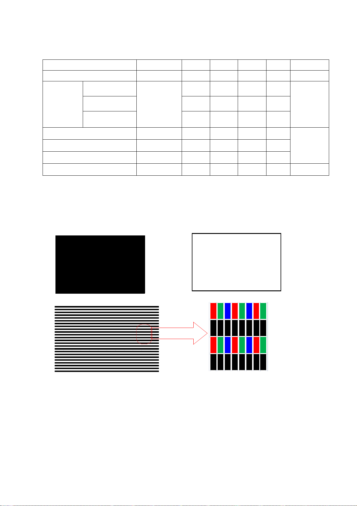
NOTE (7)
−
Y
상호 혼선(Crosstalk;Cross modulation)의 정의(DSHA): 화소간의 신호간섭에 의하여 대비비가
저하되는 현상.
)( ×
=
DRatioModulationCrosstalk
SHA
normal
YY
||
abnormalnormal
(%)100
* White Box 이외의 back ground pattern은 Gray1~ Gray64 까지 4Gray 간격으로 측정
* Horizontal Crosstalk 과 Vertical Crosstalk을 모두 측정
* 측정 결과중 가장 큰값을 Crosstalk라고 정의
참고 : Normally White mode시 Box는 Black(Gmin) /Normally Black mode시 Box는 white(Gmax)
* Crosstalk 측정 Pattern 및 Point
H
3/4H
V/4
V
V/2
Y
abnormal
Y
normal
V
3/4V
H/2
7/8H
H
H/2
Y
abnormal
Horizontal Crosstalk
7/8H
Vertical Crosstalk
Y
normal
9/38
Page 10
Note (8) (측정장비=BM-7, 측정거리=50cm)
화면의 번쩍 거림(Flicker)의 정의 : LCD Panel의 화면이 깜박거리는 현상.
ⓐ 계산식은 Flicker 측정표준에 준함.
ⓑ측정위치
(480) (960) (1440)
ACTIVE AREA
9
6
3
8
5
2
7
4
1
(270)
(540)
(810)
ⓒ 플리커 측정 패턴 (구동 방식은 1 by 1 Dot 반전구동임)
1 by 1 DOT 반전 Pattern (Total Gray 64 중 Gray #22 , #32 , #45)
:
측정
point
10/38
Page 11
7. 전기적 특성
7.1 TFT LCD 모듈
Item Symbol Min. Typ. Max. Unit Note
Voltage of Power Supply Module V
Current of
Power
(a)Black
(b)White - 650 850 mA
Supply @
Vin = 12V
(c)N PTN - 1100 1500 mA
Vsync Frequency f
Hsync Frequency f
Main Frequency f
Rush Current I
DD
I
DD
V
H
DCLK
RUSH
10.8 12.0 13.2 V (1)
- 550 700 mA
48 60.0 62.5 Hz
53 67.5 70 kHz
130 148.5 152.5 MHz
- - 4 A (4)
NOTE (1) 디스플레이 데이터 및 타이밍 신호용 콘넥터는 연결되어 있을 것(VSS= 0V)
전압치는 입력 Connector에서의 측정치임.
(2) f
= 60㎐, f
V
= 148.5㎒, VDD= 12V, DC current
DCLK
(3) 소비전력 체크 패턴
(a) Black 패턴 (b) White 패턴
(2),(3)
(Without
Inverter)
(c) N PTN
11/38
Page 12
(4) 측정조건 (12V구동, rising time =470㎲)
INPUT
POWER(12V)
CONTROL
SIGNAL
(High to
Low)
12V
㏀
47
㏀
1
㏀
47
㎌
1
R
2SK1059
0.01
2SK1339
C
㎌
Note : Control Signal : High(+12V) >Low(Ground)
All Signal lines to panel except for power 5V : Ground
The rising time of supplied voltage is controlled to 470us by R and C value.
0.9 VDD
1
㎌
12V
5V
A
V
DD
Test Point
GND
0.1 VDD
Rising Time
7.1.2 Operation temperature range at specific component
Ambient Operating
Junction Operating
Part Spec
Temperature
Temperature
Timing Controller SQ60PB 0℃ ~ 70℃ 0℃ ~ 125℃
12/38
Page 13

7.2 LED Driver (Electrical Characteristics) (Ta=25±3℃)
ITEM SYMBOL CONDITION MIN TYP MAX UNIT NOTE
Input Voltage V
Inrush Current
Note(*2)(*3)
Output Current
Note(*1)
Converter
On/Off Control
INT_DIM
EXT_DIM
(Duty)
(Duty)
I
I
I
I
ENA
V
D
F
V
D
F
T
IN
INRUSH,N
INRUSH,B
LED,N
LED,B
INT_DIM
INT_DIM
INT_DIM
EXT_DIM
EXT_DIM
EXT_DIM
RISING
22 24 26 V
VIN= 24V, Dim=Max
3D ENA = Off
VIN= 24V
3D ENA = On
- - 4.80 A Normal Mode
- - 5.30 A Blinking Mode
VIN= 24V
Dim=Max
157.0 165.0 173.0 mAmean
3D ENA = Off
VIN= 24V
3D ENA = On
266.0 280.0 294.0
Enable 3 - 5.25
Disable -0.3 - 0.4
VIN= 24V 0 - 3.3 V
VIN= 24V 1 - 100 %
VIN= 24V 140 150 160 Hz
High Level 3 - 5.25
Low Level -0.3 - 0.4
1 - 100 %
V
IN
= 24V
-
150
Note(*7)
- Hz
- - 200 ns
mAdc
Note(*5)
V
V
Normal Mode
@1string
Blinking Mode
Active High level
@1string
Note(*4)(*5)
Pin(#14)
V
EXT_DIM
: floating(N.C)
Note(*4)(*5)(*6)
V
pin(#13)
INT_DIM
= floating(N.C.)
Sync Cable should
be floating(N.C)
T
FALLING
- - 200 ns
High Level 2.4 - 3.6
V
SYNC
V
Low Level -0.3 - 0.4
D
T
T
SYNC
F
SYNC
RISING
FALLING
VIN= 24V
V
INT_DIM
= Max
V
SYNC
-50- %
- 150 - Hz
- - 200 ns
- - 200 ns
Note(*5)(*6)
INT_DIM Only
Enable 2.4 - 3.6
3D ENA
V
Disable -0.3 - 0.4
Blinking Mode
(3D)
3D PWM
D
3D_PWM
F
3D_PWM
High Level 2.4 - 3.6
Low Level -0.3 - 0.4
VIN= 24V
3D ENA = On
56 %
120 Hz
V
Note(*5)(*6)
Note
(*1) All data was approved after running 120 minutes.
(*2) Iinrush is measured within BLU on 10ms after leaving the BLU as it is at least 1hr or
more at room temperature(25℃)
13/38
Page 14

(*3) Additional Appendix for Input current
ITEM SYMBOL CONDITION
Input Current
Iovershoot,N
Vin=24V, Dim=Max
(Normal Mode)
Isaturation,N - 3.22 3.32
Iovershoot,B
Input Current
Isaturation,B - 3.54 3.65
(Blinking Mode)
Iovershoot,B - - 8.00
Vin=24V
3D PWM=56%
SPECIFICATION
MIN TYP MAX
- 3.76 3.87
- 4.15 4.25
UNIT NOTE
Amean
Amean
Amean
Amean
Amax
Overshoot Current After Turn-on
Saturation current after 1hr aging
Overshoot Current After Turn-on
Saturation current after 1hr aging
Overshoot Current After Turn-on
(*4) Internal PWM mode and External PWM mode are not available at the same time. In other word,
if one of the dimming control signal was input(connected),the other dimming control signal must be floating (No Connection)
(*5) duty=ton/ttotal
(*6) Signal rising/falling time
(*7) Use an external frequency which doesn't make a waterfall and a sound noise within this range.
14/38
Page 15

7.3 LED Drive DC-DC Converter 입/출력 Pin 사양
7.3.1 Input Connector : CN001 ( 22022WR-014B1(YEON-HO))
PIN NO SYMBOL REMARK
1,2,3,4,5 Vin Power Supply DC 24V
6,7,8,9,10 GND Ground
11 STATUS No Connection
12 ENA Converter On/Off Control Signal
13 INT_DIM
14 EXT_DIM
7.3.2 Vsync / 3D Connector : CN002 (
196047-04021-3(P-TWO)
PIN NO SYMBOL REMARK
1 Vsync Burst Mode(PWM) Signal Frequency
2 3D_ENA 3D_Mode On/Off Signal
3 3D_PWM 3D_ Mode Pulse Signal
4 GND Backlight Ground
7.3.3 Output Connector : CN003 (20037WR-H07 (YEONHO))
PIN NO SYMBOL REMARK
1 Out1 DC/DC Output
2 RESERVED RESERVED
3 RESERVED RESERVED
4 IS1 LED string1 cathode
5 IS2 LED string2 cathode
6 IS3 LED string3 cathode
7 IS4 LED string4 cathode
Internal Dimming Control Signal
No Connection (In case of using
External Dimming Control Signal
No Connection (In case of using
)
EXT_DIM
INT_DIM
#14)
#13)
15/38
Page 16

7.4 LED Drive DC-DC Converter Power Sequence
16/38
Page 17

7-5. 블럭 다이어그램(Block Diagram)
17/38
Page 18

7-6. 입력단 신호 순서(Input Terminal Pin Assignment)
7-6-1. TFT LCD 모듈(Interface signal & power)
Pin Symbol Description Pin Symbol Description Pin Symbol Description
1 TCON_WP Bus release 19 Rx1CLK- 1st, 5thLVDS Clock - 37 GND Ground
2 SCL_I I2C SCL 20 Rx1CLK+ 1st, 5thLVDS Clock + 38 Rx2[D]N 2nd, 6thLVDS Signal -
3 SDA_I I2C SDA 21 GND Ground 39 Rx2[D]P 2nd, 6thLVDS Signal +
4 3D Format 0 Not Connect (2) 22 Rx1[D]N 1st, 5thLVDS Signal - 40 Rx2[E]N 2nd, 6thLVDS Signal - (1)
5 3D_SYNC_O
6 3D Format 1 Not Connect (2) 24 Rx1[E]N 1st, 5thLVDS Signal - (1) 42 N.C Not Connect
7 N.C Not Connect 25 Rx1[E]P 1st, 5thLVDS Signal + (1) 43 N.C Not Connect
8 N.C Not Connect 26 3D_EN 3D_EN signal 44 GND Ground
9 N.C Not Connect 27 N.C Not Connect 45 GND Ground
10 N.C Not Connect 28 Rx2[A]N 2nd, 6thLVDS Signal - 46 GND Ground
11 GND Ground 29 Rx2[A]P 2nd, 6thLVDS Signal + 47 N.C Not Connect
12 Rx1[A]N 1st, 5thLVDS Signal - 30 Rx2[B]N 2nd, 6thLVDS Signal - 48 12V DC power supply
13 Rx1[A]P 1st, 5thLVDS Signal + 31 Rx2[B]P 2nd, 6thLVDS Signal + 49 12V DC power supply
14 Rx1[B]N 1st, 5thLVDS Signal - 32 Rx2[C]N 2nd, 6thLVDS Signal - 50 12V DC power supply
15 Rx1[B]P 1st, 5thLVDS Signal + 33 Rx2[C]P 2nd, 6thLVDS Signal + 51 12V DC power supply
16 Rx1[C]N 1st, 5thLVDS Signal - 34 GND Ground
17 Rx1[C]P 1st, 5thLVDS Signal + 35 Rx2CLK- 2nd, 6thLVDS Clock -
18 GND Ground 36 Rx2CLK+ 2nd, 6thLVDS Clock +
ShutterGlass sync
output signal
23 Rx1[D]P 1st, 5thLVDS Signal + 41 Rx2[E]P 2nd, 6thLVDS Signal + (1)
<51PIN>
Note(1) :
- Input Mode 8Bit Setting & 8bit input 시, ==> E_Chanel : Floating
- Input Mode 10bit Setting & 8bit input 시, ==> E_Chanel : Keep Level '0'
PIN No.24 / Pin No.40 : Pull Up
PIN No.25 / Pin No.41 : Pull Down
* Level of LVDS signals are base on LVDS CHARACTERISTICS(7-12)
NOTE(2) : 3D input format selection
- FORMATI[1:0] : 2’b0x = Line interleave , 2’b10 = side/side , 2’b11 = top/bottom
18/38
Page 19

NOTE(2) Parameter Symbol
Interface
Input High Voltage FORMAT[1] 2.0 - 3.6 V
Input Low Voltage FORMAT[0] -0.3 - 0.8 V
7-7. 입력신호와 표시색상과의 관계
Value
Min Typ Max
Unit Note
COLOR DISPLAY
BLACK 0 0 0 0 0 0 0 0 0 0 0000000000 0000000000 -
BLUE 0000000000 0000000000 1111111111 -
GREEN 0 0 0 0 0 0 0 0 0 0 1111111111 0000000000 -
BASIC
COLOR
GRAY
SCALE OF
RED
GRAY
SCALE OF
GREEN
GRAY
SCALE OF
BLUE
CYAN 0000000000 1111111111 1111111111 -
MAGENTA 1 1 1 1 1 1 1 1 1 1 0000000000 1111111111 -
YELLOW 1 1 1 1 1 1 1 1 1 1 1111111111 0000000000 -
WHITE 1 1 1 1 1 1 1 1 1 1 1111111111 1111111111 -
BLACK 0 0 0 0 0 0 0 0 0 0 0000000000 0000000000 R0
DARK
LIGHT
BLACK 0 0 0 0 0 0 0 0 0 0 0000000000 0000000000 G0
DARK
LIGHT
GREEN 0 0 0 0 0 0 0 0 0 0 1111111111 0000000000 G1023
BLACK 0 0 0 0 0 0 0 0 0 0 0000000000 0000000000 B0
DARK
LIGHT
BLUE 0000000000 0000000000 1111111111 B1023
DATA SIGNAL
RED GREEN BLUE
R0 R1 R2 R3 R4 R5 R6 R7 R8
RED 1111111111 0000000000 0000000000 -
1000000000 0000000000 0000000000 R1
↑
↓
RED 1111111111 0000000000 0000000000 R1023
↑
↓
↑
↓
0100000000 0000000000 0000000000 R2
:::::::::: :::::::::: ::::::::::
:::::::::: :::::::::: ::::::::::
1011111111 0000000000 0000000000 R1021
0111111111 0000000000 0000000000 R1022
0000000000 1000000000 0000000000 G1
0000000000 0100000000 0000000000 G2
:::::::::: :::::::::: ::::::::::
:::::::::: :::::::::: ::::::::::
0000000000 1011111111 0000000000 G1021
0000000000 0111111111 0000000000 G1022
0000000000 0000000000 1000000000 B1
0000000000 0000000000 0100000000 B2
:::::::::: :::::::::: ::::::::::
:::::::::: :::::::::: ::::::::::
0000000000 0000000000 1011111111 B1021
0000000000 0000000000 0111111111 B1022
R9 G0 G1 G2 G3 G4 G5 G6 G7 G8 G9 B0 B1 B2 B3 B4 B5 B6 B7 B8 B9
GRAY
SCALE
LEVEL
R3~
R1020
G3~
G1020
B3~
B1020
NOTE
(1) Gray 정의 :
Rn : 빨강색 Gray, Gn : 녹색 Gray, Bn : 파란색 Gray (n=Gray level)
(2) 입력신호 : 0=Low level voltage, 1=High level voltage
19/38
Page 20

7-8. Time parameter(DE Mode)
SIGNAL ITEM SYMBOL MIN. TYP. MAX. UNIT NOTE
Clock
Hsync Fh 53 67.5 70 KHz
Frequency
Cycle
1/TC 130 148.5 152.5 MHz
Vsync Fv 48 60 62.5 Hz
Vertical Active
Disply Term
Horizontal
Active
Display Term
Display
Period
Vertical
Total
Display
Period
Horizontal
Total
TVD 1080 lines
TVB 1110 1125 1400 lines
THD 1920 clocks
TH 2092 2200 2348 clocks
→ 본 제품은 H-sync와 V-sync신호도 필히 입력되어야 함
→ 위 조건을 벗어날 때에는 BIST 동작함 (Pattern : Black)
Parameter Symbol
Min Typ Max
Input High
(High) 2.5 - 3.3 V
V
IH
(Low) 0 - 0.5 V
V
IL
CMOS
Interface
Threshold
Voltage
Input Low
Threshold
Voltage
Value
Unit Note
20/38
Page 21

7-9. 인터페이스 신호의 타이밍 다이어그램( DE Only Mode)
T
V
T
VD
DE
T
T
HD
DE
D
CLK
T
VB
H
T
C
DATA
SIGNALS
D
CLK
DISPLAY
DATA
DE
Odd Data
Even Data
T
C
T
CH
T
DS
T
ES
T
CL
0.5 V
CC
T
DH
0.5 V
CC
0.5 V
CC
21/38
Page 22

7-10. LVDS Interface
- LVDS Receiver : Tcon내장형
- JEDIA 10bit 규격 채용
差動信號
TxOUT/RxIN0
TxOUT/RxIN1
LVDS pin JEIDA -DATA
TxIN/RxOUT0 R4
TxIN/RxOUT1 R5
TxIN/RxOUT2 R6
TxIN/RxOUT3 R7
TxIN/RxOUT4 R8
TxIN/RxOUT6 R9
TxIN/RxOUT7 G4
TxIN/RxOUT8 G5
TxIN/RxOUT9 G6
TxIN/RxOUT12 G7
TxIN/RxOUT13 G8
TxIN/RxOUT14 G9
TxIN/RxOUT15 B4
TxIN/RxOUT18 B5
TxIN/RxOUT19 B6
TxOUT/RxIN2
TxOUT/RxIN3
TxOUT/RxIN4
TxIN/RxOUT20 B7
TxIN/RxOUT21 B8
TxIN/RxOUT22 B9
TxIN/RxOUT24 HSYNC
TxIN/RxOUT25 VSYNC
TxIN/RxOUT26 DEN
TxIN/RxOUT27 R2
TxIN/RxOUT5 R3
TxIN/RxOUT10 G2
TxIN/RxOUT11 G3
TxIN/RxOUT16 B2
TxIN/RxOUT17 B3
TxIN/RxOUT23 RESERVED
TxIN/RxOUT28 R0
TxIN/RxOUT29 R1
TxIN/RxOUT30 G0
TxIN/RxOUT31 G1
TxIN/RxOUT32 B0
TxIN/RxOUT33 B1
TxIN/RxOUT34 RESERVED
22/38
Page 23

7-11. 전원 온/오프 순서(Power ON/OFF Sequence)
: Latch-up이나 LCD 모듈의 DC operation을 막기위해 전원 온/오프 순서는 아래와 같아야 함.
T
Power Supply V
0.1V
Vss
DD
DD
1
0.9V
0.9V
T
2
DD
DD
0.1V
D
D
T
T
3
Interface Signal
(Digital data)
Vss
Power ON
VALID
Power OFF
4
T
5
0.5Vcc 0.5Vcc
T
6
Power Supply
For B/L unit
1<T1≤10msec
1<T2≤50msec
0<T3≤50msec
1sec≤T4
≤
1,000msec
100 msec≤T6 (Recommend Value)
NOTE
(1) 모듈에 신호를 인가하는 외부장치의 전원은 V
(2) LCD 동작 범위내에서 램프의 전압을 인가 할 것. LCD가 동작되기 전에 램프를 켜거나
램프를 끄기전에 LCD를 끌 때, 화면에 NOISE가 발생함..
(3) V
가 인가된 후 인터페이스 신호가 들어가지 않는 상태(Interface Signal High
DD
Impedence)로 장시간 두지 말 것.
(4) Power Off후 재 Power On하기 전에 제품이 완전히 방전후 측정.
T5
와 같아야 한다.
DD
23/38
Page 24

7-12. LVDS CHARACTERISTICS (SQ60P 기준)
-. DC Specification.
-. AC Specification.
24/38
Page 25

25/38
Page 26

7-13. SPREAD SPECTRUM SPEC
- Modulation frequency : max 300 kHz
- Modulation rate : max +/- 1.5%
7-14. 3D 구동 GUIDE
1) 3D INPUT SOURCE 정의
LTA460HQ18-C01 모델의 3D 구동을 위해서는
60Hz Frame sequential 방식의 3D 구동 Source가 인가되어야 함.
타 Format의 3D 구동Source 지원 안됨.
2) INPUT PIN 정의
PIN Number PIN 명 정의
3D_EN 신호 High(3.3V)시, 3D 동작함.
26 3D_EN
Normally GND.
SET에서 화면과 Shutter Glass간의 3D_SYNC를 맞추기 위한 입력.
5 3D_SYNC_I
Sequence 하기 참조.
4,6
3D_Format 0
3D_Format 1
3D input format selection
FORMAT I[1:0] : 2'b0x = Line interleave , 2'b10 = side/side
※3D Signal Sequence는 하기와 같이 입력되어야함.
26/38
Page 27

8. 신뢰성 평가 조건
시험
항목
HTOL 50 ℃ 0/8 0/4 0/4 0/4
HTOL 2 60 ℃ 0/4 0/4 0/4 0/4
LTOL -5 ℃ 0/4 0/4 0/4 0/4
LTOL 2 -10℃ 각 5hr 이상 방치후 상온상습 1hr 이상 on 0/4 0/4 0/4 0/4
THB 50 ℃ / 80 %RH 0/4 0/4 0/4 0/4
HTS 70 ℃ 0/4 0/4 0/4 0/4
LTS -25 ℃ 0/4 0/4 0/4 0/4
WHTS 60 ℃ / 75 %RH 0/4 0/4 0/4 0/4
TS -20℃,30분 ~ 60℃,30분, 100cycle 0/4 0/4 0/4 0/4
ALTITUDE
(감압)
ESD
진동 10~300Hz/1.5G/10minSR,XYZ,30min/axis 0/3 0/3 0/3 0/3
.보관/동작복합:-10℃~50℃, 54hrs
17,000ft(5,000m)/동작.40,000ft(12,000m)/비동작)
.구동: 23,000ft 25℃ 10hrs
.구동 접촉:±10 kV, 210 Point, 1회/Point
.구동 비접촉:±20 kV ,210 Point,1회/Point
Inverter input pin:±15kV,150㎊/330, 3회/Pin
Class C 평가조건
1,2 등급 3,4 등급
ES CS ES CS
0/2 0/2 0/2 0/2
0/3 0/3 0/3 0/3
판정 시료수
±XYZ축각각1회
충격
Pallet평가 별도표준참조(DG00477 LCD 포장재 평가 일반표준) 1 1 1 1
단기잔상 50~60 ℃ Mosaic pattern(9*10) 12hrs fix 0/8 0/4 0/4 0/4
고온잔상
소음
분진
TSS
HALT -30~100℃ 15Grms 0/2 0/2 0/2 0/2
수명 평가 25 ~ 50 ℃ Time to Fail(Optional) 0/2 0/2 0/2 0/2
Twist 평가
EOS 평가 본문표 참조 0/2 0/2 0/2 0/2
DC 평가
Ball Drop
평가
(optional)
40" 이하 50G , 11msec (±XYZ)
46" 40G , 11msec (±XY , ±Z:30G)
52" 이상 30G , 11msec (±XYZ)
50~60 ℃ Mosaic pattern(9*10)
TV : 336hrs DID : 504hrs
전자기음 : 밴드별 소음값 만족할 것(Max 23dB)
열팽창 수축음 : Max 50dB (36dB 이상 5회 이하)
상온,상습 5초분사 5분낙하 5hr
10분 간격 전원 On/Off, DID는 Portrait 진행
-20℃~65℃ , TV:440cyc, 52SNB 204cyc
DID:110cyc, 52SNB 51cyc
46"이상 10도 0.7s/회 1000회
40" 20도 0.85s/회 250회
32" 20도 0.7s/회 250회
26" 20도 0.6s/회 250회
+DC: 30V 2hr 상온 상습
+DC -20V 10hr 상온상습
액정량, CS타켓치에서 ±2%로 액정량 Split별 3매
20cm 높이, 24p/panel타격
HTS(70℃) 방치, 168hr 단위로 500hr까지 평가
0/3 0/3 0/3 0/3
0/4 0/4 0/4 0/4
0/2 0/2 0/2 0/2
0/2 0/2 0/2 0/2
0/4 0/4 0/4 0/4
0/4 0/4 0/4 0/4
0/2 0/2 0/2 0/2
0/15 0/15 0/15 0/15
27/38
Page 28

수은뭉침평가
(optional)
Smear 평가
(optional)
Power on/off
평가
ASG 저온마진
평가
ASG 고온마진
평가
-5℃/60℃, 1,000회, On:3s이상/OFF:2s이상 0/4 0/4 0/4 0/4
Max. 주파수, 0℃~-50℃ 노이즈 발생온도확인 Sampling Plan 참조
-5℃ 관전류 min. 500hr 구동
초기치 후기치 X-Ray 촬영 후 비교
Tip:10mm, 6kgf, Hold:2s, 10회 0/3 0/3 0/3 0/3
Min. 주파수, 60℃ 고온구동, 96hr Sampling Plan 참조
0/4 0/4 0/4 0/4
※ 3,4 등급의 경우 시험항목 선정은PDR/BRN 시 계획된 plan 에 의거, 변경 부분 관련된
평가 항목을 선택하여 test 할수 있으며 시료 수는 상기 부속서를 따른다.
※ DVR 평가에 따른 개선검증이 완료된 후에도(E/S 평가) 등급에 상관
없이 C/S 제품에 대해, 추가 검증 필요 항목을 선택하여 실시 토록 한다.
단, 평가 시간은 등급에 따라 96~336시간으로 판정할 수 있다.
※ Pallet 평가 조건 및 기준은 LCD 포장재 평가 일반 표준(DG00477)을 참조 하여
진행한다.
※ 모든 평가의 Sampling은 본문 마지막에 있는 Sampling Plan을 참조하여 test 진행한다.
28/38
Page 29

9. PACKING
9-1. CARTON(Internal Package)
(1) Packing Form
Corrugated fiberboard box and corrugated cardboard as shock absorber
(2) Packing Method
-
Packing
-
Packing
상태 보관 기준
상태 장기 보관 기준
29/38
Page 30

9-2. Packing Specification
Item Specification Remark
LCD Packing
Pallet 1Box / Pallet 1. Pallet weight = 8.8 kg
Packing Direction Vertical
Total Pallet Size H x V x height 1270 mm(H) x 1150 mm(V) x 844 mm(height)
24ea / (Packing-
Pallet Box)
1 10.8 Kg / LCD (1ea)
2. 12 Kg / Cushion-pallet (2ea)
3. 8 Kg / Packing-Pallet Box (1ea)
>. Cushion-pallet Material : paper
>. Packing-Pallet Box Material : DW4
Total Pallet Weight 288 kg
10. MARKING & OTHERS
A nameplate bearing followed by is affixed to a shipped product at the
specified location on each product.
(1) Parts number : LTA460HQ18-C01
(2) Revision : One letter
(3) Control : One letter
(4)Lotnumber:8J5G01014D
(5) Nameplate Indication
Pallet(8.8 kg) + Module(10.8*24=259.2Kg) +
Cushion(up+botton=12kg) + Pallet-BOX(8kg)
① ③④⑤ ⑥⑦
①8:Line
②J:Device
③5:Year
④G:Month
⑤010:LOTNO
⑥14:GLASSNO
⑦D:CELLNO
LTA460HQ18-C01
1050
MADE IN KOREA
(6) Bar code marking for Customer
The bar code marking is attached to module backside.
8J5G01014D
30/38
Page 31

1) MODEL NAME : LTA460HQ18-C01
2) SAMSUNG
3) MADE IN KOREA
4) PRODUCTION NUMBER
5) USER MODEL NAME
Bar code shows a) user model name, b) production number
a) User model name
LTA460HQ18-C01
b) Production Number
SAMSUNG
MADE IN KOREA
SERIAL NO
B
REVISION CODE
*6430008B*
(7) Packing box attach
MADEIN KOREA
DEVICE : LTA460HM06-C01
TYPE :
QUANTTY : 1 PCS
CO6040001
LTA460HQ18-C01
PRODUCTION MONTH
PRODUCTION YEAR
31/38
Page 32

11. General Precautions
14.1 Handling
(a) When the module is assembled, It should be attached to the system firmly
using every mounting holes. Be careful not to twist and bend the modules.
(b) Refrain from strong mechanical shock and / or any force to the module. In
addition to damage, this may cause improper operation or damage to the module
and LED back-light.
(c) Note that polarizers are very fragile and could be easily damaged. Do not press
or scratch the surface harder than a HB pencil lead.
(d) Wipe off water droplets or oil immediately. If you leave the droplets fora
long time, Staining and discoloration may occur.
(e) If the surface of the polarizer is dirty, clean it using some absorbent cotton or soft cloth.
(f) The desirable cleaners are water, IPA(Isopropyl Alcohol) or Hexane.
Do not use Ketone type materials(ex. Acetone), Ethyl alcohol, Toluene, Ethyl
acid or Methyl chloride. It might permanent damage to the polarizer due to
chemical reaction.
(g) If the liquid crystal material leaks from the panel, it should be kept away
from the eyes or mouth . In case of contact with hands, legs or clothes, it must
be washed away thoroughly with soap.
(h) Protect the module from static , it may cause damage to the CMOS Gate ArrayIC.
(i) Use finger-stalls with soft gloves in order to keep display clean during the
incoming inspection and assembly process.
(j) Do not disassemble the module.
(k) Do not pull or fold the lamp wire.
(l) Do not adjust the variable resistor which is located on the module.
(m) Protection film for polarizer on the module shall be slowly peeled off just before
use so that the electrostatic charge can be minimized.
(n) Pins of I/F connector shall not be touched directly with bare hands.
32/38
Page 33

14.2 Storage
ITEM Unit Min. Max.
Storage Temperature (℃) 5 40
Storage Humidity (%rH) 35 75
Storage life 12 months
-The storage room should provide good ventilation and temperature control.
-Products should not be placed on the floor, but on the Pallet away from
a wall.
-Prevent products from direct sunlight, moisture nor water; Be cautious of
Storage Condition
a build up of condensation.
-Avoid other hazardous environment while storing goods.
-If products delivered or kept in conditions of over the storage period of 3
months, the recommended temperature or humidity range,
we recommend you leave them at a temperature of 20℃ and a humidity
of 50% for 24 hours.
14.3 Operation
(a) Do not connect,disconnect the module in the "Power On" condition.
(b) Power supply should always be turned on/off by the item 6.3
"Power on/off sequence"
(c) Module has high frequency circuits. Sufficient suppression to the
electromagnetic interference shall be done by system manufacturers. Grounding
and shielding methods may be important to minimize the interference.
(d) The cable between the back-light connector and its inverter power supply shall
be a minimized length and be connected directly . The longer cable between
the back-light and the inverter may cause lower luminance of lamp(LED) and
may require higher startup voltage(Vs).
14.4 Others
(a) Ultra-violet ray filter is necessary for outdoor operation.
(b) Avoid condensation of water. It may result in improper operation or disconnection
of electrode.
(c) Do not exceed the absolute maximum rating value. ( the supply voltage variation,
input voltage variation, variation in part contents and environmental temperature,
and so on) Otherwise the module may be damaged.
(d) If the module displays the same pattern continuously for a long period of time,it
can be the situation when the image "Sticks" to the screen.
(e) This module has its circuitry PCB's on the rear side and should be handled
carefully in order not to be stressed.
33/38
Page 34

15. 환경 유해물질 관리 기준
15.1 금지물질
아래에제시하는물질에대해서는부품및디바이스등에함유되는일이있어서는안된다.
표 15.1 법률에 의해 사용이 금지되어 있는 물질
물질명
Cadmium and cadmium 화합물
PBB(plybromobiphenyl)군, PBDE (polybrominated biphenyl ethers)군
*1
*2
Polychlorinated biphenyl (PCB) 류
Polychlorinated naphthalene 류
Organic tin 화합물 (Tributhyl tin category/Triphenyl tin category)
Asbestos
Azo화합물 (용해 후 표 8.3에 나와 있는 Amine을 생성하는 화합물. 이 화합물은 인체와 지속적으로
접촉하며 생산되는 제품의 부품으로는 사용 금지되어 있다.)
*1: 포장재료에 대해서는 수은, 카드뮴, 6가 크롬, 납의 중금속 불순물 허용농도가 합계 100ppm
미만이 되도록 한다.
*2: 직접 물질을 금지하는 법은 없으나, 독일의 다이옥신 규제를 따르기 위해 금지 물질로
분류된다.
카드뮴의 경우, 아래에 제시하는 부위에 대한 사용에 대해서는 현재 금지되어 있지 않으나, 향후
규제될것이므로적극적으로전폐를목표로한다.
표 15.2 규제할 카드뮴 및 기타 화합물의 용도와 전폐 목표
용도 전폐 목표
(a) DC 모터, 스위치, 릴레이, 브레이커 등 신뢰성을 요구하는
모든기기의전기접점
(b) 형광표시장치에 함유되는 형광체
2003년 3월말
(c) Ni-Cd 전지 (신규로 출시하는 것, 다망 이미 발매 중인
Ni-Cd 전지는 2007년 3월을 전폐목표로 한다.
(d) 유리 및 유리도료의 안료, 염료 2004년 3월말
34/38
Page 35

아조화합물 중에서 분해에 의해 표16.3에 제시하는 아민이 발생할 용도의 사용을 금지한다.
표15.3 아조화합물의 분해에 의해 발생해서는 안되는 아민 일람
CAS No 아민
92-67-1 4-amonodiphenyl
92-87-5 Benzidine
95-69-2 4-chloro-o-toluidine
91-59-8 2-naphthylamine
97-56-3 o-aminoazotoluene
99-55-8 2-amino-4-nitrotoluene
106-47-8 p-chloroaniline
615-05-4 2,4-diaminoanisole
101-77-9 4,4'-diaminodiphenylmethane
91-94-1 3,3'-dichlorobenzidine
119-90-4 3,3'-dimethoxybenzidine
119-93-7 3,3'-dimethylbenzidine
838-88-0 3,3'dimethyl-4,4'-diaminodiphenylmethane
120-71-8 p-cresidine
101-14-4 4,4'-methylene-bis-(2-chloro aniline)
101-80-4 4,4'-oxideaniline
139-65-1 4,4'-thiodianiline
95-53-4 o-toluidine
95-80-7 2,4-tolluylenediamine
137-7-7 2,4,5-trimenthylaniline
90-04-0 o-anisidine
15.2 완전폐기 물질
다음의 물질은 표 16.5에 표기된 용도를 제외하고 어느 부품이나 장치에 함유되어서는 안 된다.
표 15.4 완전폐기물질
물질명
납및납화합물
수은및수은화합물
6가 크롬 화합물
PVC및PVC혼합물
PBB, PBDE 이외의 유기브롬화합물
염소화 파라핀류 (염소계 난연제/가소제)
아래의 경우에 대해서는 현상황에서 대체기술이 미확립 상태이고, 부품의 기능 및 신뢰성을
확보하는데 있어서 해당부품의 계속사용이 부득이하다고 판단하여 표8.5의 완전폐기 기일까지
완전 폐기하는 것으로 한다.
다만, 대체재료의 기술확립이 가능해진 경우는 기한을 기다리지 않고 사용금지로 한다.
또한 대체기술이 없어 법규제의 규정에 의해 제외 및 예외가 인정된 경우는 기한을 재조정한다.
35/38
Page 36

표 15.5 완전폐기물질에 대한 주요 용도 및 완전폐기 목표
물질명 용도 전폐목표
사용금지 : 아래 (a),(b),(c),(d),(e),(f),(g),(h),(i),(j),(k),(l),(m) 및 (n) 이외의 용도.
예컨데포장재,프린트배선판등에대한안료용도
(a) 액세서리를 포함한 제품의 외장부 (인체에 쉽게 접촉되는 부위)에의
사용 (플라스틱에 사용되는 안정제, 안료 등)
(b) 선재피복에 사용하는 안정제, 안료 등
(c)액세서리를포함한제품의외장부에사용하는각종합금및그도장면
(d) 신규로 출시하는 소형 씰납전지
2003년 3월말
납/
그 화합물
(e) 부품의 외부전극·리드단자 등의 납땜처리
(전기부품/반도체 디바이스/히트싱크 등)
(f) 부품·디바이스의 내부접속용 납땜, 고융점 납땜
(Pb 85wt% 미만의 주석/납땜)
(g) 브라운관 이외의 광학유리에 함유된 납
(h)납을함유하는각종합금
(i) 도료, 잉크, 저항기의 저항체
(j) 불순물로서 납을 함유하는 각종 합금
다만, 아래 합금은 첨가물로서의 납의 함유가 허용된다.
합금 종류 납 함유 허용농도
강재 0.3wt% 미만
알루미늄합금 0.4wt% 미만
동합금 4wt% 미만
(k) 2003년 3월말 이전에 출시한 소형 씰납전지
2004년 3월말
36/38
Page 37

15.3 플라스틱 중의 카드뮴 허용 농도
선재피복등의플라스틱에카드뮴및그화합물을일절참가해서는안된다.
측정기의 검출한계, 오차, 자연계에 존재하는 불순물의 혼입을 고려하여 5ppm 미만으로 한다.
이 때의 전처리방법, 측정방법에 대해서는 BS EN 1122 「Plastics - Determination of
cadmium - Wet decomposition method에 준한다.
측정은 유도결합 플라즈마 발광 분광 분석법(ICP-AES)을 표준으로 한다.
(l) 부품·디바이스의 내부접속용 고융점납땜
(Pb 85wt% 이상 함유하는 주석/납땜)
(m) 세라믹 압전소자에 함유된 납화합물
(n) 브라운관, 전자부품, 형광판에 사용되는 유리
사용금지 : 아래 (a),(b),(c) 및 (d) 이외의 용도. 예컨데 포장재, 수은전지, 시간계 등
수은 /
그 화합물
6가 크롬
화합물
폴리염화
비닐 /
그 혼합물
PBB/PBDE
이외의 유기
취소화합물
(a)소형형광등:1개당수은함유량이5mg이상인것.
(b) 산화은전지, 알칼리·망간 버튼전지, 공기전지
(c) 소형형광등 : 1개당 수은함유량이 5mg 미만인 것.
(d) 소형형광등, 직관형광등 이외의 램프
사용금지 : 아래 이외의 용도
도금, 안료 등의 성분으로 함유되는 것 2004년 3월말
폴리염화비닐을 가지는 모든 부품·디바이스
주요 용도로서 기내배선용 비닐전선, 전원코드, 외부접속코드, 기타 코드
류를 가지는 유니트 등.
다만, 안전규격의 규제를 받는 것에 대해서는 소니측이 확인한 후에 계속
하여 사용하는 경우가 있다.
프린트배선판, 외광 등 대형부품.
(안전성이 확인된 대체 난연제를 적용할 수 없는 경우, 사용을 인정한다)
상기 이외의 부위
(안전성이 확인된 대체 난연제를 적용할 수 없는 경우, 사용을 인정한다)
예외
2004년 3월말
예외
2004년 3월말
2003년 3월말
2004년 3월말
15.4 방출을 규제하는 물질
표15.6 방출을 규제하는 물질
물질명 방출 농도 주요 용도
포름알데히드
대기 중 농도 10㎥ 이상의 기밀시험실에서
0.1ppm 이하
15.5 부품, 디바이스 제조시에 사용해서는 안되는 물질
표15.7 부품, 디바이스 제조시에 사용해서는 안되는 물질
물질명
[오존층을 파괴하는 물질]
CFC(chlorofluorocarbon),HCFC(hydrochlorofluorocarbon),methyl bromide,
1,1,1-trichloroethane, carbon tetrachloride
[Chlorine 유기 용매]
1,1,2-trichloroethane, 1,2-dichloroethane, 1,1-dichloroethlene,
1,2-dichloroethylene,methylene chloride,
chloroform, trichloroethylene, tetrachloroethylene
모든 목제재료 및
목제품
37/38
 Loading...