

Page 1

製品標準
(LTA400HF28-W)
Rev01
1/35
Page 2
1.
목적
제품 정보를 정의하고 개발제품 Target을 설정하며, 이를 부서간에 공유하기 위함.
2. 적용범위
TFT LCD LTA400HF28-W
3. 일반개요
3.1 개요
LTA400HF28 은 비정질 실리콘(Amorphous Silicon) 박막 트랜지스터(TFT; Thin Film
Transistor)를 스위칭 소자로 사용한 컬러 능동 행렬(Color active matrix) 방식의 TFT 액정 표시
소자(LCD;Liquid Crystal Display) Module이다. Module은 Panel, 구동 회로부와 Backlight부로 구
성되며, Interface 방법은 Digital 영상정보를 직렬로 고속 전송하는 방식의 일종인 LVDS방식을 채
용하였다. 본 제품은 1,920 * 1,080(16:9) 화소를 포함하고, 1.07 Billion의 색상을 지원한다.
그리고 독자 기술인 SPVA Mode 기술을 적용하여 시야각은 상하좌우 89°이상을 제공하는 광시야각
제품이며, 고속 응답 속도를 지원하는 120Hz 지원 제품이다.
3.2 특징
① High Contrast Ratio & High Color Saturation
② 고속 응답 특성(120Hz 지원)
③ Wide UXGA (1,920 x 1,080 화소)급 Full HD 지원 (16:9)
④ SPVA(Super Patterned Vertical Align) Mode 광시야각(±178°)
⑤ wLED B/L Unit 설계 적용
⑥ Sync Format : DE(Data Enable) Only Mode 지원, H/V-sync Mode 지원 불가
⑦ 4Ch LVDS 인터페이스
3.3 응용분야
① Public Display
② Home-alone Multimedia TFT-LCD TV
③ High Definition TV Ready (HD TV Ready)
④ AV 제품의 화상 표시 단말기
3.4 일반사양
항목 사양 단위 비고
유효표시면적
구동소자
표현가능색 수 1.07 Billion (10bit Dithering) color
화소수
화소배열
화소크기 0.46125 (H) × 0.15375 (V) ㎜
표시모드
표면처리 반사율 1%, Hard Coating 3H Anti-Glare
885.6(H) X 498.15
(V)
㎜ 대각선 40.0"
a-Si TFT Active matrix
1,920 × 1,080 pixel 16 : 9
RGB Vertical Stripe
Normally Black
2/35
Page 3
4. 기구사양
Item Min. Typ. Max. Note
Horizontal
(H)
Module
Vertical(V) 535.3 536.3 537.3 mm
size
Depth(D)
Weight 9.0 10.0 Kg
Note(1) : wall mount stud 기준
5. 절대 최대 정격
5.1환경사양절대정격
Item Symbol Min. Max. Unit Note
Storage temperature T
Operating temperature
(Ambient temperature)
Shock ( non - operating ) Snop
920.7 921.7 922.7 mm
19.8 20.8 22.8 Note(1)
28.8 29.8 31.8 Converter
-20 65 ℃ (1)
0 50 ℃ (1)
-40
G (2),(4)
T
STG
OPR
x, y
축
z축 - 30
Vibration ( Non -
operating )
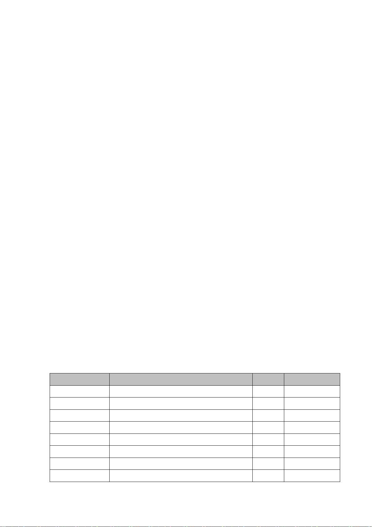
NOTE (1) 온도와 상대습도 관계는 아래 그림에 따른다.
(최대습구 온도는 39℃임 <40℃에서 93.8%RH에 해당>)
NOTE (2)
NOTE (3)
NOTE (4)
11ms, sine wave, 1 time for ±X, ±Y, ±Z axis
10-300 Hz, Sweep rate 10min, 30min for X,Y,Z axis
진동 및 충격 Test시 모듈을 고정하는 치구는 모듈이 치구에 의해 트위스트 되거나
Bent되지 않도록 충분히 견고해야 한다.
100
-40 -20 0 20 40 60
Vnop - 1.5 G (3),(4)
Relative Humidity ( %RH)
90
80
60
Operating Range
40
20
Storage Range
5
0
Temperature (
O
80
C)
3/35
Page 4
5.2 전기적 사양 절대 정격
5.2.1 TFT LCD MODULE 절대 정격
ITEM SYMBOL MIN. MAX. UNIT NOTE
Power Supply Voltage/ Display VDD VSS-0.5 VDD+10% V (1)
(VSS = 0 V)
NOTE(1)
동작온도 범위안에서
.
5.2.2 LED UNIT Absolute Maximum Rating
항 목 기호 최대정격 단위 비고
Operating temperature range Top -20~70 ℃
Storage temperature range Tstg -30~70 ℃
Junction Temperature Tj
If
110
0.14
Forward current
0.28
35
Forward voltage
Thermal resistance, Junction
to PCB
Ifp
Vf 108.5 V
Rth,JS
℃
A
A
K/W
Continuous operation @String
(2 String/PCB)
Duty 40% operation @ String
(2 String/PCB)
Continuous operation @String
(2 String/PCB)
4/35
Page 5
6. 광학 특성
측정 환경
6.1
환경 조건
-.
온도
:25℃±2℃/
습도
무풍(직접적인 바람 제거)/무진동
-. Warm-Up T ime :
①최소30분이상
②주기적(약15초간격)으로
현재 휘도 차이의 비가
:25%~85%RH/
압력
:86kPa~106kPa/
center
0.5%
휘도를 측정하여10분전 휘도와
이하가 되는 최초 시점
암실
:1Lux
이하
/
측정 장비
6.2
-.
종류
BM-5A(TOPCON社), BM-7(TOPCON社), SR-3(TOPCON社), RD-80S(TOPCON社),
:
PR-650(Photo Reserch社),
측정 거리 및 방향
-.
T
warm-up
=(|Lum
t-10
-Lum
now
where , Lum
(LMD : Light Measurement Device)
EZ-Contrast(Eldim社)
:
θ=90°± 0.3°
d= 50Cm
|/Lum
t-10
now
는10분전 휘도
LMD
) × 100 < 0.5
,Lum
가되는시간
는현재휘도
now
LCD
LMD Field
BM-5A / SR-3 2°
BM-7 / RD-80S 2°/ 1°
PR-650 1°
구동 조건
6.3
-. TFT LCD Module:V
= 12.0V, fV=120㎐,fDCLK=297㎒,Column
DD
반전 구동
-. BACK-LIGHT UNIT : Total Lamp Current = 140 mA / Duty 100 %
5/35
Page 6
6.4
광학 특성
ITEM SYMBOL MIN. TYP. MAX. UNIT LMD NOTE
Luminance of White
(center)
Contrast Ratio (center)
Brightness Uniformity
(9point or 13Point)
Red
Color
Green
Chromaticity
(CIE 1931)
Blue
White
Color Gamut
Y
L,AVG
CR
Buni
Rx
Ry
Gx
Gy
Bx
By 0.060
Wx
330 400 - ㏅/㎡
3,000 5,000 -
- -25
0.640
0.330
0.300
typ.
-0.03
0.600
0.150
0.280
0.290Wy
-
69 72 -
typ.
+0.03
-
SR-3
(1)
%
-
SR-3
Center
Point
%
Color Temperature
Viewing Angle
(CR≥10)
Crosstalk
Flicker
GAMMA
Response time
Hor.
Ver.
GtoG
평균
CCT
θ
θ
θ
L
R
H
7,000 10,000 13,000
79 89 -
79 89 -
79 89 -
K
Degrees
(2)
EZ
θ
L
101-255
SHA
20-100
0-19
F
-
D
79 89 -
- - 5.0
- - 15.0
--X(
관리안함
)
-210
1.9 2.2 2.5
-815
%(3)
-
BM-7
PI
(4)*
기재
불가
ms (5)
6/35
Page 7
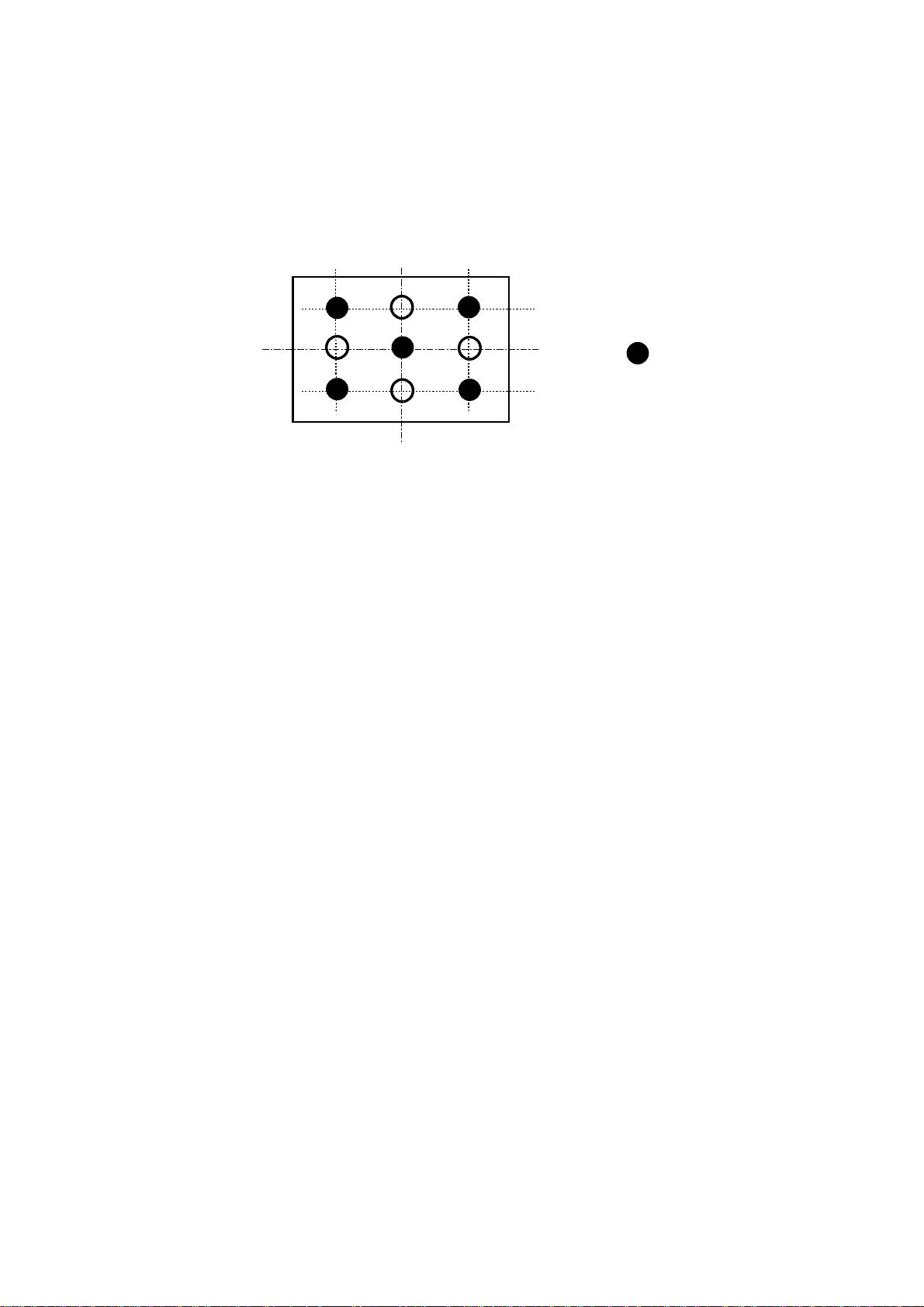
NOTE (1)
측정위치 : 판넬상 측정위치는 9개 점으로 한다.
ACTIVE AREA
(320) (960) (1600)
9
6
3
NOTE (2) 대비비(C/R : Contrast ratio)
: 측정위치 중앙(Point ⑤)에서 White 상태(G
판넬상에서
C/R =
NOTE (3) White 휘도의 정의
판넬상에서
(YL):
측정위치 중앙(Point ⑤)의 white 휘도(YL) 를 측정한 값.
8
5
2
WHITE
BLACK
7
4
1
상태 휘도
상태 휘도
(180)
(540)
(900)
)와 Black 상태(G
MAX
: test point
)의 비로 정의.
MIN
NOTE (4) Brightness Uniformity(Buni) :
측정 화면 : Fully White
측정화면상의 9개의 휘도를 측정, 아래와 같이 정의한다.
B B
max min
−
max
B
× 100
where, Bmax = Maximum brightness
Bmin = Minimum brightness
7/35
Page 8
NOTE (5)
▶응답시간
(Response time)
사이로 변화하는 시간의 합
Black(TFT OFF) Black(TFT OFF)White(TFT ON)
Optical
Response
100%
90%
10%
0%
NOTE (6)
시야각(Viewing angle)의 정의 : C/R이 10이상되는 시각의 범위
의정의:화면이 어두워 질 때와 밝아질 때에 투과율이
T
R
T
F
Time
10%와90%
8/35
Page 9
NOTE (7) 상호 혼선(Crosstalk;Cross modulation)의 정의(D
−
Y
비가 저하되는 현상.
): 화소간의 신호간섭에 의하여 대비
SHA
)( ×
=
DRatioModulationCrosstalk
SHA
normal
YY
||
abnormalnormal
(%)100
* White Box 이외의 back ground pattern은 Gray1~ Gray64 까지 4Gray 간격으로 측정
* Horizontal Crosstalk 과 Vertical Crosstalk을 모두 측정
* 측정 결과중 가장 큰값을 Crosstalk라고 정의
참고 : Normally White mode시 Box는 Black(Gmin) /Normally Black mode시 Box는 white(Gmax)
* Crosstalk 측정 Pattern 및 Point
H
3/4H
V/4
V
V/2
Y
abnormal
Y
normal
V
3/4V
H/2
7/8H
H
H/2
Y
abnormal
Horizontal Crosstalk
7/8H
Vertical Crosstalk
Y
normal
9/35
Page 10
Note (8) (측정장비=BM-7, 측정거리=50cm)
화면의 번쩍 거림(Flicker)의 정의 : LCD Panel의 화면이 깜박거리는 현상.
ⓐ 계산식은 Flicker 측정표준에 준함.
ⓑ측정위치
(480) (960) (1440)
ACTIVE AREA
9
6
3
8
5
2
7
4
1
(270)
(540)
(810)
ⓒ 플리커 측정 패턴 (구동 방식은 1 by 1 Dot 반전구동임)
1 by 1 DOT 반전 Pattern (Total Gray 64 중 Gray #22 , #32 , #45)
:
측정
point
10/35
Page 11

7. 전기적 특성
7.1 TFT LCD 모듈
Item Symbol Min. Typ. Max. Unit Note
Voltage of Power Supply Module V
Current of
Power
Supply
(a) Black
(b) White - 660 750 mA
(c) Sub_V_Stripe - 1000 1100 mA
Vsync Frequency f
Hsync Frequency f
Main Frequency f
Rush Current I
DD
I
DD
V
H
DCLK
RUSH
10.8 12.0 13.2 V (1)
- 660 750 mA
95 120 125 Hz
120 135 140 kHz
260 297 305 MHz
-46A (4)
NOTE (1) 디스프레이 데이터 및 타이밍 신호용 콘넥터는 연결되어 있을 것(V
전압치는 입력 Connector에서의 측정치임.
(2) f
= 120㎐, f
V
=297㎒,VDD=12V,DCcurrent
DCLK
(3) 소비전력 체크 패턴
(a) Black 패턴 (b) White 패턴
(2),(3)
(Without
Inverter)
Column Driving
=0V)
SS
(c) Sub_V_Stripe 패턴
(4) 측정조건 (12V구동, rising time =470㎲)
11/35
Page 12

7.1.1 Operation temperature range at specific component
Ambient Operating
Junction Operating
Part Spec
Temperature
Temperature
Timing Controller S128B 0℃ ~ 70℃ -20℃ ~ 125℃
12/35
Page 13

7.2 LED Converter (Ta=25℃)
7.2.1 Electrical Characteristics
Item Symbol Condition
Spec.
단위 비고
Min Typ Max
Input Voltage V
Input Current I
Output Current I
Operating
Frequency
Backlight
on/off Control
Error Out
Internal PWM
Dimming Mode
in
inrush,N
LED,N
f
op
ENA
Z
Normal
Z
Abnormal
V
dim
f
dim
D
dim
(duty)
22.0 24.0 26.0 V
Vin=24.0V,
dim=max
--4.1A
Vin=22.0~26.0V,
dim=max
133 140 147
Vin=22.0~26.0V,
dim=max
113 123 133
Enable 2.4 - 5.5 V
Disable -0.3 - 0.8 V
Normal - - 1.3k
Abnormal 1 - -
0-3.3V
Vin=22.0~26.0V
140 150 160
=22.0~26.0V,
V
in
V
=3.3V
dim
=22.0~26.0V,
V
in
=0V
V
dim
100 - - %
1
-
note
dc
㎃
mean
note
㎑
Ω
㏁
open Collector
㎐
note
V
→
-%
(*2)(*3)
(*1)
(*4)(*5)
pin(#14)
ex-dim
floating(N.C)
External PWM
Dimming Mode
V
D
f
t
t
ex-dim
ex-dim
ex-dim
rising
falling
High Level 2.4 - 5.5 V
Low Level -0.3 - 0.8 V
95 - 200
1100%
Vin=22.0~26.0V
--200
--200
13/35
㎐
㎱
㎱
(*4)(*5)(*6)
note
V
pin(#13)
dim
→
floating(N.C)
Sync Cable
Should be
floating (N.C)
Page 14

Note
(*1)
All data was approved after running 120 minutes.
(*2)
I
is measured within BLU on 10㎳ after leaving the BLU as it is at least 1hr or moreat
inrush
room temperature(25℃)
(*3)
Additional Appendix for Input current
Item Symbol Condition
Spec.
단위 비고
Min Typ Max
Input Current
(*4)
words, if one of the dimming control signal was input (connected), the other dimming contro
l signal must be floating (No Connection)
In case of External PWM mode, The Vsync Connector (Sync Cable) should be floating (No C
onnection)
(*5)
I
overshoot
I
saturation
Vin=24.0V,
dim=max
- 2.63 2.70 A
- 2.55 2.59 A
Maximum Current during 1hr aging
dc
Saturation Current after 1hr aging
dc
Internal PWM mode and External PWM mode are not available at the same time. Inother
duty=ton/t
total
t
total
t
on
(*6)
signal rising/falling time
90%
10%
t
r
t
f
14/35
Page 15

블럭 다이어그램
8.
(Block Diagram)
8.1 TFT LCD Module
USER CONNECTOR
DC/DC CONVERTER
(AVDD/HAVDD
VSS/VDD/1.2V
VONE/VOFFE/CKV)
COLTROL
DATA
VIN(12V)
AVDD
CKV
VCOM
Υ
Voltage
VCC(3.3V)
VCC(1.8V)
VCC(1.2V)
HAVDD
REGULATOR
CONTROL PCB
T-CON
(AIPI)
GAMMA-GEN.
VCOM-GEN
FFC
SOURCE PCB
FFC
SOURCE PCB
DATA Dr.IC
(966CH)X3
L7400GL1 PANEL
1920 x 1080 x RGB
DATA Dr.IC
(966CH)X3
15/35
Page 16

8.2 Back Light Unit
LED 62 EA
LED 62 EA
16/35
Page 17

9. 입력단 신호 순서(Input Terminal Pin Assignment)
9.1 TFT LCD 모듈(Interface signal & power)
Pin Description Pin Description
1 Vdd (12V) 26
2 Vdd (12V) 27 Rx3[1]N
3 Vdd (12V) 28 Rx3[1]P
4 Vdd (12V) 29 Rx3[2]N
5 Vdd (12V) 30 Rx3[2]P
6 N.C 31 GND
7 GND 32 Rx3CLK-
8 GND 33 Rx3CLK+
9 GND 34 GND
10
11 Rx1[0]P 36 Rx3[3]P
12 Rx1[1]N 37 Rx3[4]N
Rx1[0]N 35 Rx3[3]N
connector :
Odd
LVDS
Signal
CN1 FI-RE41S-HF (JAE, UJU)
Rx3[0]P
13 Rx1[1]P 38 Rx3[4]P
14 Rx1[2]N 39 GND
15 Rx1[2]P 40 No connection
16 GND 41 No connection
17 Rx1CLK-
18 Rx1CLK+
19 GND
20 Rx1[3]N
21 Rx1[3]P
22 Rx1[4]N
23 Rx1[4]P
24 GND
25 Odd LVDS Rx3[0]N
Odd
LVDS
Signal
NOTE1
(NOTE1) NOT CONNECTED : THIS PINS ARE ONLY USED FOR SEC INTERNAL OPERATIONS.
(NOTE2) LVDS SELECTION OPTION : HIGH(3.3V)→Normal , LOW(GND) & Default→Jeida
17/35
Page 18

connector :
CN2 FI-RE51S-HF (JAE, UJU)
Pin Description Pin Description
1 Vdd (12V) 26
Rx4[0]P
2 Vdd (12V) 27 Rx4[1]N
3 Vdd (12V) 28 Rx4[1]P
4 Vdd (12V) 29 Rx4[2]N
5 Vdd (12V) 30 Rx4[2]P
6 N.C 31 GND
7 GND 32 Rx4CLK-
8 GND 33 Rx4CLK+
Even
LVDS
Signal
9 GND 34 GND
10
Rx2[0]N 35 Rx4[3]N
11 Rx2[0]P 36 Rx4[3]P
12 Rx2[1]N 37 Rx4[4]N
13 Rx2[1]P 38 Rx4[4]P
14 Rx2[2]N 39 GND
15 Rx2[2]P 40 No connection
16 GND 41 No connection
Even
LVDS
17 Rx2CLK- 42 No connection
Signal
18 Rx2CLK+ 43 No connection
NOTE1
19 GND 44 No connection
20 Rx2[3]N 45 LVDS_SEL NOTE2
21 Rx2[3]P 46 DCC ON/OFF Option NOTE3
22 Rx2[4]N 47 No connection
23 Rx2[4]P 48 No connection
24 GND 49 No connection
25 Even LVDS Rx4[0]N 50 No connection
51 No connection
NOTE1) NOT CONNECTED : THIS PINS ARE ONLY USED FOR SEC INTERNAL OPERATIONS.
Note 2) LVDS OPTION : IF THIS PIN : HIGH (3.3 V)
OTHERWISE : LOW (GND) OR OPEN(NC)
Note 3) DCC Option : IF THIS PIN : HIGH (3.3 V)→DCC on
OTHERWISE : LOW (GND) OR Open(NC)
Sequence : On = V
OFF = Interface Signal(T3)≥LVDS Option≥V
(T1)≥LVDS Option≥Interface Signal(T2)
DD
→
NORMAL NS LVDS FORMAT
→
JEIDALVDSFORMAT
→
DCC off
DD
18/35
Page 19

9.2 LED Drive DC-DC Converter입/
출력
Pin
사양
9.2.1 CN1 CONNECTOR : 20022WR-14B1(YEONHO)
Pin No. Symbol Remark
1~5 VIN Input Supply Voltage (24V)
6~10 GND Power/Signal Ground
11 Error_Out
12 ENA Converter On/Off Control Signal
13 V
14 V
dim
ex-dim
Operation Status Output
Normal : GND, Abnormal : Open Collector
DC Dimming Control Signal (0~3.3V)
No Connection (In case of using V
External Dimming Control Signal (1~100%)
No Connection (In case of using V
9.2.2 LED Drive DC-DC Converter Power Sequence
90%
Vin(24V)
10%
20ms(min)
V
(0~3.3V)
dim
ex-dim
dim
#14)
#13)
0.5s(min)
V
0s(min)
0.5s(min)
ex-dim
(E xt ernal PW M di mm ing)
0s(min)
ENA
0.2s(min)
19/35
Page 20

입력신호와 표시색상과의 관계
9.3
COLOR DISPLAY
BLACK 000000000000000000000000 -
BLUE 000000000000000011111111 -
GREEN 000000001111111100000000 -
BASIC
COLOR
GRAY
SCALE
OF
RED
GRAY
SCALE
OF
GREEN
GRAY
SCALE
OF
BLUE
CYAN 000000001111111111111111 -
RED 111111110000000000000000 -
MAGENTA111111110000000011111111 -
YELLOW111111111111111100000000 -
WHITE 111111111111111111111111 BLACK 000000000000000000000000 R0
DARK
↑
↓
LIGHT
RED 111111110000000000000000 R255
BLACK 000000000000000000000000 G0
DARK
↑
↓
LIGHT
GREEN 000000001111111100000000 G255
BLACK 000000000000000000000000 B0
DARK
↑
↓
LIGHT
BLUE 000000000000000011111111 B255
DATA SIGNAL
RED GREEN BLUE
R0 R1 R2 R3 R4 R5 R6 R7 G0 G1 G2 G3 G4 G5 G6 G7 B0 B1 B2 B3 B4 B5 B6 B7
100000000000000000000000 R1
010000000000000000000000 R2
::::::::::::::::::::::::
::::::::::::::::::::::::
101111110000000000000000 R253
011111110000000000000000 R254
000000001000000000000000 G1
000000000100000000000000 G2
::::::::::::::::::::::::
::::::::::::::::::::::::
000000001011111100000000 G253
000000000111111100000000 G254
000000000000000010000000 B1
000000000000000001000000 B2
::::::::::::::::::::::::
::::::::::::::::::::::::
000000000000000010111111 B253
000000000000000001111111 B254
GRAY
SCALE
LEVEL
R3~
R252
G3~
G252
B3~
B252
NOTE
Gray
(1)
입력신호
(2)
Rn :
정의
:
빨강색
Gray, Gn :
녹색
Gray, Bn :
: 0=Low level voltage, 1=High level voltage
20/35
파란색
Gray (n=Gray level)
Page 21

10. 인터페이스 타이밍
10.1 Time parameter (DE Mode)
-
SIGNAL ITEM SYMBOL MIN. TYP. MAX. UNIT NOTE
Clock Frequency 1/T
Frame Frequency Cycle T
Vertical Active
Disply Term
Display Period T
Vertical Total T
Display Period T
C
v
VD
VB
HD
260 297 305
95 120 125 Hz
- 1080 - lines
1092 1125 1350 lines
- 1920 - clocks
Horizontal Active
Display Term
Horizontal
Total
T
H
2090 2200 2350 clocks
→ 본 제품은 H-sync와 V-sync신호도 필히 입력되어야 함
㎒
2 Pixels/clk
21/35
Page 22

10.2 인터페이스 신호의 타이밍 다이어그램( DE Mode)
T
V
T
VD
DE
T
HD
DE
D
CLK
T
VB
T
H
T
C
DATA
SIGNALS
D
CLK
DISPLAY
DATA
T
C
T
CH
T
DS
T
ES
T
CL
0.5 V
CC
T
DH
0.5 V
CC
DE
22/35
0.5 V
CC
Page 23

10.3 LVDS Interface
LVDS Receiver : Tcon(merged)내장형
-
- JEIDA & Normal Data Format
LVDS OPTION(
입력
45pin) : IF THIS PIN : HIGH (3.3 V)
OTHERWISE : OPEN or LOW (GND)
差動信號
TxOUT/RxIN0
TxOUT/RxIN1
→
NORMAL NS LVDS FORMAT
→
JEIDALVDSFORMAT
LVDS pin JEIDA -DATA Normal -DATA
TxIN/RxOUT0 R2 R0
TxIN/RxOUT1 R3 R1
TxIN/RxOUT2 R4 R2
TxIN/RxOUT3 R5 R3
TxIN/RxOUT4 R6 R4
TxIN/RxOUT6 R7 R5
TxIN/RxOUT7 G2 G0
TxIN/RxOUT8 G3 G1
TxIN/RxOUT9 G4 G2
TxIN/RxOUT12 G5 G3
TxIN/RxOUT13 G6 G4
TxIN/RxOUT14 G7 G5
TxOUT/RxIN2
TxOUT/RxIN3
TxIN/RxOUT15 B2 B0
TxIN/RxOUT18 B3 B1
TxIN/RxOUT19 B4 B2
TxIN/RxOUT20 B5 B3
TxIN/RxOUT21 B6 B4
TxIN/RxOUT22 B7 B5
TxIN/RxOUT24 HSYNC HSYNC
TxIN/RxOUT25 VSYNC VSYNC
TxIN/RxOUT26 DEN DEN
TxIN/RxOUT27 R0 R6
TxIN/RxOUT5 R1 R7
TxIN/RxOUT10 G0 G6
TxIN/RxOUT11 G1 G7
TxIN/RxOUT16 B0 B6
TxIN/RxOUT17 B1 B7
TxIN/RxOUT23 RESERVED RESERVED
23/35
Page 24

10.4 전원 온/오프 순서(Power ON/OFF Sequence)
10.4.1 TFT-LCD Module
: Latch-up이나 LCD 모듈의 DC operation을 막기 위해 전원 온/오프 순서는 아래와 같아야 함.
0.9 VDD 0.9 VDD
Power Supply
V
DD
0V
0.1 VDD
0.1 VDD
0 ≤T1 ≤ 10msec
2 ≤ 50 msec
0 ≤ T
0 ≤ T
3 ≤ 50 msec
1sec ≤ T
4
Signals
0 V
Back-light(Recommended)
500 msec ≤ T
1000
2500
5
100 msec ≤ T6
T1
T2
Power On
T3
T4
VALID
Power Off
50% 50%
T5 T6
NOTE
(1)
(2) LCD
(3) V
(4) Power Off
모듈에 신호를 인가하는 외부장치의 전원은
동작 범위내에서
거나
DD
Impedence)
를끄기전에
LED
가 인가된 후 인터페이스 신호가 들어가지 않는 상태
로 장시간 두지 말 것
후재
Power On
의 전압을 인가 할 것
LED
를끌때,화면에
LCD
.
하기 전에 제품이 완전히 방전후 측정
24/35
와 같아야 한다
V
DD
NOISE
.
가 동작되기 전에
.LCD
가 발생할 수 있음
(Interface Signal High
를켜
LED
.
.
Page 25

11. PACKING
11.1 Carton
(1) Packing Form
Corrugated fiberboard box and EPS cushion as shock absorber
(2) Packing
11.2. Packing
방법
상태 보관 기준
11.3. Packing
상태 장기 보관 기준
11.4. Packing Specification
Item Specification Remark
21ea / (Packing-Pallet
1.
Kg / LCD (1ea)
9.0
LCD Packing
Box)
2. 14.0 Kg / Packing Pallet Box (1set)
Pallet 1Box / Pallet Pallet weight = 14.5 kg
Packing Direction Vertical
Total Pallet Size H x V x height 1150 mm(L) x 985 mm(W) x 708 mm(H)
Pallet(14.5kg) + Module
kg) + Packing Pallet
(189
Total Pallet Weight 218.34kg
Box(14kg) + Desiccant(0.04kgx=21=0.84kg)
25/35
Page 26

13. General Precautions
13.1 Handling
(a) When the module is assembled, It should be attached to the system firmly
using every mounting holes. Be careful not to twist and bend the modules.
(b) Refrain from strong mechanical shock and / or any force to the module. In
addition to damage, this may cause improper operation or damage to the module
and CCFL back-light.
(c) Note that polarizers are very fragile and could be easily damaged. Do not press
or scratch the surface harder than a HB pencil lead.
(d) Wipe off water droplets or oil immediately. If you leave the droplets for a
long time, Staining and discoloration may occur.
(e) If the surface of the polarizer is dirty, clean it using some absorbent cotton or
soft cloth.
(f) The desirable cleaners are water, IPA(Isopropyl Alcohol) or Hexane.
Do not use Ketone type materials(ex. Acetone), Ethyl alcohol, Toluene, Ethyl
acid or Methyl chloride. It might permanent damage to the polarizer due to
chemical reaction.
(g) If the liquid crystal material leaks from the panel, it should be kept away
from the eyes or mouth . In case of contact with hands, legs or clothes, it must
be washed away thoroughly with soap.
(h) Protect the module from static , it may cause damage to the CMOS Gate Array
IC.
(i) Use finger-stalls with soft gloves in order to keep display clean during the
incoming inspection and assembly process.
(j) Do not disassemble the module.
(k) Do not pull or fold the lamp wire.
(l) Do not adjust the variable resistor which is located on the module.
(m) Protection film for polarizer on the module shall be slowly peeled off just before
use so that the electrostatic charge can be minimized.
(n) Pins of I/F connector shall not be touched directly with bare hands.
26/35
Page 27

13.2 Storage
(a) Do not leave the module in high temperature, and high humidity for a long time.
It is highly recommended to store the module with temperature from 0 to 35C
and relative humidity of less than 70%.
(b) Do not store the TFT-LCD module in direct sunlight.
(c) The module shall be stored in a dark place. It is prohibited to apply sunlight or
fluorescent light during the store.
13.3 Operation
(a) Do not connect,disconnect the module in the "Power On" condition.
(b) Power supply should always be turned on/off by the item 6.3
"Power on/off sequence"
(c) Module has high frequency circuits. Sufficient suppression to the
electromagnetic interference shall be done by system manufacturers. Grounding
and shielding methods may be important to minimize the interference.
(d) The cable between the back-light connector and its inverter power supply shall
be a minimized length and be connected directly . The longer cable between
the back-light and the inverter may cause lower luminance of lamp(CCFL) and
may require higher startup voltage(Vs).
13.4 Others
(a) Ultra-violet ray filter is necessary for outdoor operation.
(b) Avoid condensation of water. It may result in improper operation or disconnection
of electrode.
(c) Do not exceed the absolute maximum rating value. ( the supply voltage variation,
input voltage variation, variation in part contents and environmental temperature,
and so on) Otherwise the module may be damaged.
(d) If the module displays the same pattern continuously for a long period of time,it
can be the situation when the image "Sticks" to the screen.
(e) This module has its circuitry PCB's on t he rear side and should be handled
carefully in order not to be stressed.
27/35
Page 28

14.환경유해물질관리기준
14.1 금지물질
아래에제시하는물질에대해서는부품및디바이스등에함유되는일이있어서는안된다.
표 14.1 법률에 의해 사용이 금지되어 있는 물질
물질명
Cadmium and cadmium 화합물
PBB(plybromobiphenyl)군, PBDE (polybrominated biphenyl ethers)군
*1
*2
Polychlorinated biphenyl (PCB) 류
Polychlorinated naphthalene 류
Organic tin 화합물 (Tributhyl tin category/Triphenyl tin category)
Asbestos
Azo화합물 (용해 후 표 8.3에 나와 있는 Amine을 생성하는 화합물. 이 화합물은 인체와
지속적으로 접촉하며 생산되는 제품의 부품으로는 사용 금지되어 있다.)
*1: 포장재료에 대해서는 수은, 카드뮴, 6가 크롬, 납의 중금속 불순물 허용농도가 합계 100ppm
미만이 되도록 한다.
*2: 직접 물질을 금지하는 법은 없으나, 독일의 다이옥신 규제를 따르기 위해 금지 물질로
분류된다.
카드뮴의 경우, 아래에 제시하는 부위에 대한 사용에 대해서는 현재 금지되어 있지 않으나, 향후
규제될 것이므로 적극적으로 전폐를 목표로 한다.
표14.2 규제할 카드뮴 및 기타 화합물의 용도와 전폐 목표
용도 전폐 목표
(a) DC 모터, 스위치, 릴레이, 브레이커 등 신뢰성을 요구하는
모든기기의전기접점
(b) 형광표시장치에 함유되는 형광체
2003년 3월말
(c) Ni-Cd 전지 (신규로 출시하는 것, 다망 이미 발매 중인
Ni-Cd 전지는 2007년 3월을 전폐목표로 한다.
(d) 유리 및 유리도료의 안료, 염료 2004년 3월말
28/35
Page 29

아조화합물 중에서 분해에 의해 표14.3에 제시하는 아민이 발생할 용도의 사용을 금지한다.
표14.3 아조화합물의 분해에 의해 발생해서는 안되는 아민 일람
CAS No 아민
92-67-1 4-amonodiphenyl
92-87-5 Benzidine
95-69-2 4-chloro-o-toluidine
91-59-8 2-naphthylamine
97-56-3 o-aminoazotoluene
99-55-8 2-amino-4-nitrotoluene
106-47-8 p-chloroaniline
615-05-4 2,4-diaminoanisole
101-77-9 4,4'-diaminodiphenylmethane
91-94-1 3,3'-dichlorobenzidine
119-90-4 3,3'-dimethoxybenzidine
119-93-7 3,3'-dimethylbenzidine
838-88-0 3,3'dimethyl-4,4'-diaminodiphenylmethane
120-71-8 p-cresidine
101-14-4 4,4'-methylene-bis-(2-chloro aniline)
101-80-4 4,4'-oxideaniline
139-65-1 4,4'-thiodianiline
95-53-4 o-toluidine
95-80-7 2,4-tolluylenediamine
137-7-7 2,4,5-trimenthylaniline
90-04-0 o-anisidine
14.2 완전폐기 물질
다음의 물질은 표 14.5에 표기된 용도를 제외하고 어느 부품이나 장치에 함유되어서는 안 된다.
표 14.4 완전폐기물질
물질명
납및납화합물
수은및수은화합물
6가 크롬 화합물
PVC및PVC혼합물
PBB, PBDE 이외의 유기브롬화합물
염소화 파라핀류 (염소계 난연제/가소제)
29/35
Page 30

아래의 경우에 대해서는 현상황에서 대체기술이 미확립 상태이고, 부품의 기능 및 신뢰성을
확보하는데 있어서 해당부품의 계속사용이 부득이하다고 판단하여 표8.5의 완전폐기 기일까지
완전 폐기하는 것으로 한다.
다만, 대체재료의 기술확립이 가능해진 경우는 기한을 기다리지 않고 사용금지로 한다.
또한 대체기술이 없어 법규제의 규정에 의해 제외 및 예외가 인정된 경우는 기한을 재조정한다.
표 14.5 완전폐기물질에 대한 주요 용도 및 완전폐기 목표
물질명 용도 전폐목표
사용금지 : 아래 (a),(b),(c),(d),(e),(f),(g),(h),(i),(j),(k),(l),(m) 및 (n) 이외의
용도. 예컨데 포장재, 프린트배선판 등에 대한 안료 용도
(a) 액세서리를 포함한 제품의 외장부 (인체에 쉽게 접촉되는 부위)에의
사용 (플라스틱에 사용되는 안정제, 안료 등)
(b) 선재피복에 사용하는 안정제, 안료 등
2003년 3월
말
(c)액세서리를포함한제품의외장부에사용하는각종합금및그도장면
(d) 신규로 출시하는 소형 씰납전지
(e) 부품의 외부전극·리드단자 등의 납땜처리
(전기부품/반도체 디바이스/히트싱크 등)
(f) 부품·디바이스의 내부접속용 납땜, 고융점 납땜
납/
그 화합물
(Pb 85wt% 미만의 주석/납땜)
(g) 브라운관 이외의 광학유리에 함유된 납
(h)납을함유하는각종합금
(i) 도료, 잉크, 저항기의 저항체
(j) 불순물로서 납을 함유하는 각종 합금
2004년 3월
말
다만, 아래 합금은 첨가물로서의 납의 함유가 허용된다.
합금 종류 납 함유 허용농도
강재 0.3wt% 미만
알루미늄합금 0.4wt% 미만
동합금 4wt% 미만
(k) 2003년 3월말 이전에 출시한 소형 씰납전지
14.3 플라스틱 중의 카드뮴 허용 농도
선재피복등의플라스틱에카드뮴및그화합물을일절참가해서는안된다.
측정기의 검출한계, 오차, 자연계에 존재하는 불순물의 혼입을 고려하여 5ppm 미만으로 한다.
이 때의 전처리방법, 측정방법에 대해서는 BS EN 1122 「Plastics - Determination of
cadmium - Wet decomposition method에 준한다.
측정은 유도결합 플라즈마 발광 분광 분석법(ICP-AES)을 표준으로 한다.
30/35
Page 31

수은 /
그 화합물
6가 크롬
화합물
폴리염화
비닐 /
그 혼합물
PBB/PBDE
이외의 유기
취소화합물
(l) 부품·디바이스의 내부접속용 고융점납땜
(Pb 85wt% 이상 함유하는 주석/납땜)
예외
(m) 세라믹 압전소자에 함유된 납화합물
(n) 브라운관, 전자부품, 형광판에 사용되는 유리
사용금지 : 아래 (a),(b),(c) 및 (d) 이외의 용도. 예컨데 포장재, 수은전지, 시간계 등
(a)소형형광등:1개당수은함유량이5mg이상인것.
(b) 산화은전지, 알칼리·망간 버튼전지, 공기전지
(c) 소형형광등 : 1개당 수은함유량이 5mg 미만인 것.
2004년 3월말
예외
(d) 소형형광등, 직관형광등 이외의 램프
사용금지 : 아래 이외의 용도
도금, 안료 등의 성분으로 함유되는 것 2004년 3월말
폴리염화비닐을 가지는 모든 부품·디바이스
주요 용도로서 기내배선용 비닐전선, 전원코드, 외부접속코드, 기타 코드
류를 가지는 유니트 등.
2004년 3월말
다만, 안전규격의 규제를 받는 것에 대해서는 소니측이 확인한 후에 계속
하여 사용하는 경우가 있다.
프린트배선판, 외광 등 대형부품.
2003년 3월말
(안전성이 확인된 대체 난연제를 적용할 수 없는 경우, 사용을 인정한다)
상기 이외의 부위
(안전성이 확인된 대체 난연제를 적용할 수 없는 경우, 사용을 인정한다)
2004년 3월말
14.4 방출을 규제하는 물질
표14.6 방출을 규제하는 물질
물질명 방출 농도 주요 용도
대기 중 농도 10㎥ 이상의 기밀시험실에서
포름알데히드
0.1ppm 이하
14.5 부품, 디바이스 제조시에 사용해서는 안되는 물질
표14.7 부품, 디바이스 제조시에 사용해서는 안되는 물질
물질명
[오존층을 파괴하는 물질]
CFC(chlorofluorocarbon),HCFC(hydrochlorofluorocarbon),methyl bromide,
1,1,1-trichloroethane, carbon tetrachloride
[Chlorine 유기 용매]
1,1,2-trichloroethane, 1,2-dichloroethane, 1,1-dichloroethlene,
1,2-dichloroethylene,methylene chloride,
chloroform, trichloroethylene, tetrachloroethylene
모든 목제재료 및
목제품
31/35
 Loading...