

Page 1
SAMSUNG TFT-LCD
Samsung Secret
Product Information
DATE : 26. Mar. 2012
MODEL :
The Information Described in this Specification is Preliminary and can be changed without
prior notice
LTA320HN05 (FHD, 60HZ)
LCD Business
Samsung Electronics Co . , LTD.
MODEL LTA320HN05 Doc. No 05-000-G-20120326 Page
1/25
Page 2
Contents
Revision History -------------------------------------------------------------------------------------------- (3)
General Description --------------------------------------------------------------------------------------- (4)
General Information --------------------------------------------------------------------------------------- (4)
1. Absolute Maximum Ratings -------------------------------------------------------------------------- (5)
2. Optical Characteristics --------------------------------------------------------------------------------- (6)
3. Electrical Characteristics ------------------------------------------------------------------------------- (9)
Samsung Secret
3.1 TFT LCD Module
3.2 Back Light Unit
4. Input Terminal Pin Assignment --------------------------------------------------------------------- (11)
4.1 Input Signal & Power
4.2 . LS Bar Input Pin Configuration
4.3 LVDS Interface
4.4 Input Signals, Basic Display Colors and Gray Scale of Each Color
5. Interface Timing ---------------------------------------------------------------------------------------- (16)
5.1 Timing Parameters (Stand Alone Mode)
5.2 Timing Diagrams of interface Signal (D mode)
5.3 Power ON/OFF Sequence
6. Outline Dimension -------------------------------------------------------------------------------------- (19)
7. Packing -------------------------------------------------------------------------------------------------- (21)
8. Marking & Others --------------------------------------------------------------------------------------- (22)
9. General Precaution ------------------------------------------------------------------------------------ (23)
9.1 Handling
9.2 Storage
9.3 Operation
9.4 Operation Condition Guide
9.5 Others
MODEL LTA320HN05 Doc. No 05-000-G-20120326 Page
2/25
Page 3
* Revision History
Samsung Secret
Date
26.
Mar,
2012
Rev.
No
000 - First Issued
Page Summary
MODEL LTA320HN05 Doc. No 05-000-G-20120326 Page
3/25
Page 4
General Description
Samsung Secret
Description
LTA320XXXX is a color active matrix liquid crystal display (LCD) that uses amorphous
silicon TFT(Thin Film Transistor) as switching components. This model is composed of a
TFT LCD panel, a driver circuit and a back light unit. The resolution of a 32.0“ is 1920 x
1080 and this model can display up to 1.07G colors with wide viewing angle of 89° or
higher in all directions. This panel is intended to support applications to provide a excellent
performance for Flat Panel Display such as Home-alone Multimedia TFT-LCD TV, Display
terminals for AV application products, and High Definition TV (HDTV).
Features
RoHS compliance (Pb-free)
High contrast ratio, high aperture ratio, fast response time
SPVA (Super Patterned Vertical Align) mode
Wide viewing angle (±89°)
Full HD (1920 x 1080 pixels) resolution (16:9)
Low Power consumption
WLED (White Light Emitting Diode) Backlight
LVDS (Low Voltage Differential Signaling) interface
General Information
Items Specification Unit Note
Module Size
Weight 4800(Max) g
Pixel Pitch
Active Display Area 698.4(H) x 392.85(V) mm
Surface Treatment Haze 0.8%, Hard-coating (2H)
Display Colors 8+2 bit- 1.07G colors
Number of Pixels 1920 x 1080 pixel
Pixel Arrangement RGB Vertical stripe
Display Mode Normally Black
Luminance of White 450 cd/m
727.6(H
0.12125(H) × 0.36375(V)* 3
) x 424.0(V
TYP
26.0(D
MAX
)
TYP
)
mm
mm
±1.0mm
2
Typ.
MODEL LTA320HN05 Doc. No 05-000-G-20120326 Page
4/25
Page 5
Samsung Secret
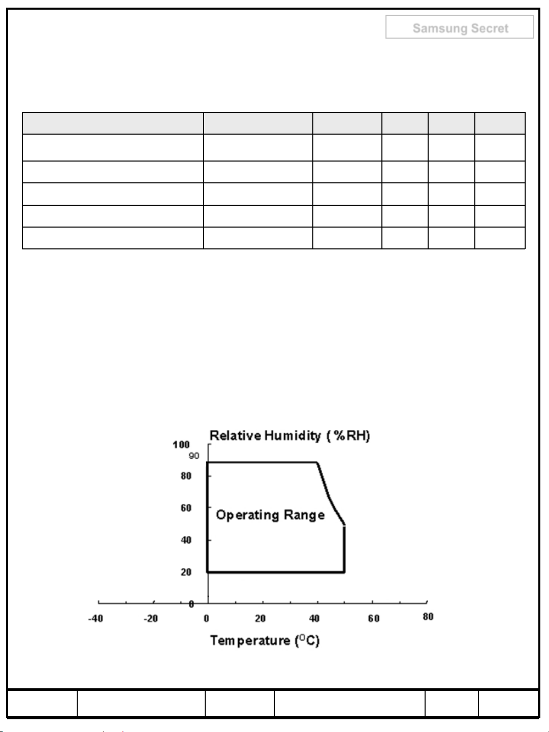
1. Absolute Maximum Ratings
1-1 Operating Condition
If the condition exceeds maximum ratings, it can cause malfunction or unrecoverable
damage to the device.
Item Symbol Min. Max. Unit Note
Power Supply Voltage V
Module Storage Temperature T
Operating Temperature T
Shock ( non – operating ) S
Vibration ( non – operating ) V
Note (1) Ta= 25 ± 2 °C
(2) Temperature and relative humidity range are shown in the figure below.
a. 93.8 % RH Max. (Ta ≤ 40 °C)
b. Maximum wet-bulb temperature at 40 °C or less. (Ta ≤ 40 °C)
c. No condensation
(3) Polarizer will not be damaged in this range, even though abnormal visual problems occur
in T
(4) 11ms, sine wave, one time for ±X, ±Y, ±Z axis
(5) 10-300 Hz, Sweep rate 10min, 30min for X, Y, Z axis
SUR
range.
DD
STG
OPR
NOP
NOP
GND-0.5 13 V (1)
-20 60
0 50
℃
℃
- 50 G (4)
- 1.5 G (5)
(2)
(2)
(40, 93.8)
(50, 50.4)
Fig. Temperature and Relative humidity range
MODEL LTA320HN05 Doc. No 05-000-G-20120326 Page
5/25
Page 6
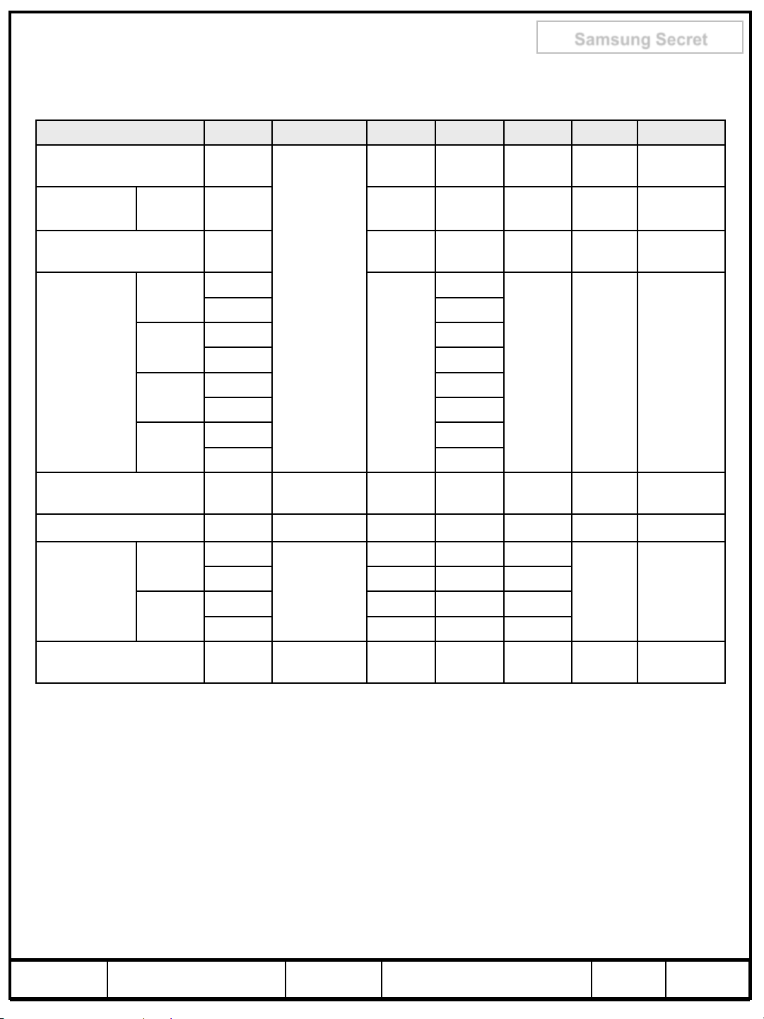
2. Optical Characteristics
The optical characteristics should be measured in a dark room or equivalent.
Measuring equipment : TOPCON BM-7,SPECTRORADIOMETER SR-3
Samsung Secret
(LED Input Current = 110mA, Ta = 25 ± 2°C, VDD=12V, fv= 60Hz, f
Item Symbol Condition Min. Typ. Max. Unit Note
Contrast Ratio
(Center of screen)
Response
Time
G-to-G
[AVE]
Luminance of White
(Center of screen)
Red
Color
Green
Chromaticity
(CIE 1931)
Blue
White
Color Gamut - - 70 - %
C/R
*3000 5000 -
Tg - 8 16 msec
Y
L
380 450 - cd/m
Normal
Rx
Ry 0.332
Gx 0.312
Gy 0.606
Bx 0.155
qL,R=0
qU,D=0
Viewing
Angle
0.640
TYP.
-0.03
By 0.053
Wx 0.280
Wy 0.285
=148.5MHz, Dim = 100%)
DCLK
RD-80S
2
TYP.
+0.03
(3)
SR-3A
(5)
(6)
SR-3A
(7),(8)
SR-3A
(7)
SR-3A
Color Temperature - - 10000 - K (9)
Hor.
Viewing
Angle
Ver.
Brightness Uniformity
(9 Points)
q
L
q
R
q
U
q
D
B
uni
C/R≥10
79 89 79 89 -
Degree
79 89 79 89 -
- - 30 %
* CR = (White at point ⑤ of Note 2) / (Most Dark Point of Black Pattern at area ⓐ of Note 2)
Note (1) Test Equipment Setup
The measurement should be executed in a stable, windless and dark room between
40min and 60min after lighting the back light at the given temperature for stabilization
of the back light. This should be measured in the center of screen.
Single lamp current @ Vdim = 100%
Environment condition : Ta = 25 ± 2 °C
(8)
EZ-Contrast
(4)
SR-3
MODEL LTA320HN05 Doc. No 05-000-G-20120326 Page
6/25
Page 7
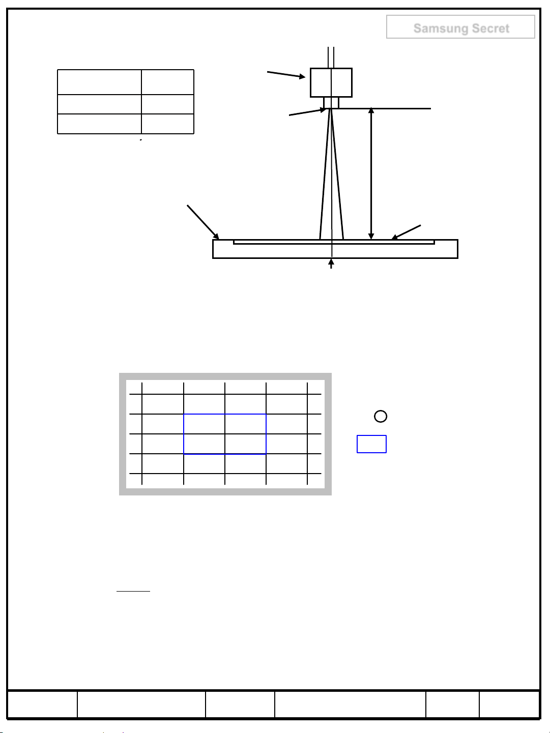
Samsung Secret
C R
G
G
/
max
min
Photo detector Field
SR-3
BM-7
TFT - LCD Module
Note (2) Definition of test point
320 960 1600
1°
2°
Photo detector
Field
SR-3 : 50㎝
BM-7 : 50㎝
LCD Panel
The center of the screen
180
540
900
Note (3) Definition of Contrast Ratio (C/R)
: Ratio of gray max (Gmax) & gray min (Gmin) at the center point ⑤ of the panel
⑨
Area ⓐ
⑥
640 1280
Gmax : Luminance with all pixels white
Gmin : Luminance with all pixels black
⑧
⑤ ④
②③
⑦
①
360
720
Active Area
Test Point
CR Measured Area
MODEL LTA320HN05 Doc. No 05-000-G-20120326 Page
7/25
Page 8
Note (4) Definition of 9 points brightness uniformity
Buni
B B
B
100
( max min)
max
Gamma X Y
X Z B B B
Y Measurement Level Z Measurement Brightness
B Maximum Brightness B Minimum Brightness
lum
lum
log log
: / :
: / :
min max min
max min
100 100
100
Bmax : Maximum brightness
Bmin : Minimum brightness
Note (5) Definition of Response time : Sum of Tr, Tf
Samsung Secret
Display data
Optical Instruments
Response
Note (6) Definition of Luminance of White : Luminance of white at center point ⑤
Note (7) Definition of Color Chromaticity (CIE 1931)
Color coordinate of Red, Green, Blue & White at center point ⑤
Note (8) Definition of Viewing Angle
: Viewing angle range (C/R ≥10)
100%
90%
10%
0%
Black (data off)
T
R
White (data on)
White (data off)
T
F
TIME
Note (9) Definition of 2 point Gamma
MODEL LTA320HN05 Doc. No 05-000-G-20120326 Page
8/25
Page 9

Samsung Secret
3. Electrical Characteristics
3.1 TFT LCD Module
The connector for display data & timing signal should be connected.
Ta = 25°C ± 2 °C
Item Symbol Min. Typ. Max. Unit Note
Voltage of Power Supply V
(a) Black
Current
(b) White - 360 400
of Power
Supply
(c) Mosaic - 350 390
DD
I
DD
11 12 13 V (1)
- 330 380
(4) Max Pattern - 580 650
Vsync Frequency f
Hsync Frequency f
Main Frequency f
Rush Current I
V
H
DCLK
RUSH
47 60 62 Hz
50 67.5 73 kHz
130 148.5 155 MHz
- - 3 A (4)
Note (1) The ripple voltage should be controlled under 10% of VDD.
(2) fV=60Hz, fDCLK = 148.5MHz, VDD= 12.0V, DC Current.
(3) Power dissipation check pattern (LCD Module only)
a) Black Pattern b) White Pattern c) Mosaic d) Max. Pattern
mA (2),(3)
(4) Measurement Conditions
V
100%
DD
90%
10%
GND
T
=470us
RUSH
Rush Current I
can be measured when T
RUSH
RUSH
. is1ms
MODEL LTA320HN05 Doc. No 05-000-G-20120326 Page
9/25
Page 10

Samsung Secret
3.2 Back Light Unit
The back light contains 60 LEDs.
The characteristics of lamps are shown in the following tables.
Item Symbol Min. Typ. Max. Unit Note
Operating Life Time Hr 30,000 - - Hour (1)
Ta=25 ± 2°C
Operating
Current
Operating
Voltage
Range of Voltage
Note (1) It is defined as the time to take until the brightness reduces to 50% of its original value at
each Srting, Iop=.110.0mArms
[Definition of Operating Voltage : At each Strings, Iop= 140.0 mArms (typ.)]
Continuous Iop - 110 200 mA
Continuous Vop 171 - 194 V
⊿Vf
- - 11.5 V
@140mA
/ 30LEDs
@Ta 25℃
@140mA
/ String
3.2.1 Review and Update for Electrical Specification
According to the improvement of efficiency for devices, the electrical specification would be revie
wed and revised after initial values had been established.This revision mentioned above should be
discussed at appropriate time.
MODEL LTA320HN05 Doc. No 05-000-G-20120326 Page
10/25
Page 11

4. Input Terminal Pin Assignment
4.1. Input Signal & Power of Control Board
1. 51Pin Connector : FI-RNE51SZ-HF (JAE)
Samsung Secret
PIN No. Signal Description
1 Vin Power 26 RE[0]P Even LVDS Signal +
2 Vin Power 27 RE[1]N Even LVDS Signal 3 Vin Power 28 RE[1]P Even LVDS Signal +
4 Vin Power 29 RE[2]N Even LVDS Signal 5 Vin Power 30 RE[2]P Even LVDS Signal +
6 N.C. No Connection 31 GND GND
7 GND GND 32 RECLKN Even LVDS CLK 8 GND GND 33 RECLKP Even LVDS CLK +
9 GND GND 34 GND GND
10 RO[0]N Odd LVDS Signal - 35 RE[3]N Even LVDS Signal -
11 RO[0]P Odd LVDS Signal + 36 RE[3]P Even LVDS Signal +
12 RO[1]N Odd LVDS Signal - 37 RE[4]N Even LVDS Signal 13 RO[1]P Odd LVDS Signal + 38 RE[4]P Even LVDS Signal +
PIN
No.
Signal Description
14 RO[2]N Odd LVDS Signal - 39 GND GND
15 RO[2]P Odd LVDS Signal + 40 N.C. No Connection
16 GND GND 41 N.C. No Connection
17 ROCLKN Odd LVDS CLK - 42 N.C. No Connection
18 ROCLKP Odd LVDS CLK + 43 N.C. No Connection
19 GND GND 44 N.C. No Connection
20 RO[3]N Odd LVDS Signal - 45 N.C. No Connection
21 RO[3]P Odd LVDS Signal + 46 N.C. No Connection
22 RO[4]N Odd LVDS Signal - 47 N.C. No Connection
23 RO[4]P Odd LVDS Signal + 48 N.C. No Connection
24 GND GND 49 N.C. No Connection
25 RE[0]N Even LVDS Signal - 50 N.C. No Connection
51 LVDS OPT LVDS Option
MODEL LTA320HN05 Doc. No 05-000-G-20120326 Page
11/25
Page 12

■ Option Pin Description
These pins are CMOS interface.
Please use within the range of the following restriction.
VIH:2.4V(min) / 3.5V(max)
VIL:0.0V(min) / 0.4V(max)
Note(1) Pin number starts from Right side
PCB
▼
Samsung Secret
A. 51 Pin
#1
CON1
#1
#51
#51
Fig. Connector diagram
a. All GND pins should be connected together and also be connected to the LCD’s
metal chassis.
b. All power input pins should be connected together.
c. All NC pins should be separated from other signal or power.
MODEL LTA320HN05 Doc. No 05-000-G-20120326 Page
12/25
Page 13

4.2. LS Bar Input Pin Configuration
1. CONNECTOR : Morex/51103-040
Samsung Secret
Pin
1
2 N.C.
3 N.C.
4 DC Voltage (+)
2. CONNECTOR : Morex/51103-0500
Pin
1
2
3
4
5
Pin Configuration (Function)
DC Voltage (+)
Pin Configuration (Function)
Feedback
N.C.
N.C.
Feedback
N.C.
MODEL LTA320HN05 Doc. No 05-000-G-20120326 Page
13/25
Page 14

4.3 LVDS Interface
TxOUT/RxIN0
TxOUT/RxIN1
TxOUT/RxIN2
TxOUT/RxIN3
TxOUT/RxIN4
Samsung Secret
LVDS pin Odd Data Even Data
TxIN/RxOUT0 R4 R4
TxIN/RxOUT1 R5 R5
TxIN/RxOUT2 R6 R6
TxIN/RxOUT3 R7 R7
TxIN/RxOUT4 R8 R8
TxIN/RxOUT6 R9 R9
TxIN/RxOUT7 G4 G4
TxIN/RxOUT8 G5 G5
TxIN/RxOUT9 G6 G6
TxIN/RxOUT12 G7 G7
TxIN/RxOUT13 G8 G8
TxIN/RxOUT14 G9 G9
TxIN/RxOUT15 B4 B4
TxIN/RxOUT18 B5 B5
TxIN/RxOUT19 B6 B6
TxIN/RxOUT20 B7 B7
TxIN/RxOUT21 B8 B8
TxIN/RxOUT22 B9 B9
TxIN/RxOUT24 HSYNC HSYNC
TxIN/RxOUT25 VSYNC VSYNC
TxIN/RxOUT26 DEN DEN
TxIN/RxOUT27 R2 R2
TxIN/RxOUT5 R3 R3
TxIN/RxOUT10 G2 G2
TxIN/RxOUT11 G3 G3
TxIN/RxOUT16 B2 B2
TxIN/RxOUT17 B3 B3
TxIN/RxOUT23 Reserved Reserved
TxIN/RxOUT28 R0 R0
TxIN/RxOUT29 R1 R1
TxIN/RxOUT30 G0 G0
TxIN/RxOUT31 G1 G1
TxIN/RxOUT32 B0 B0
TxIN/RxOUT33 B1 B1
TxIN/RxOUT34 Reserved Reserved
MODEL LTA320HN05 Doc. No 05-000-G-20120326 Page
14/25
Page 15

4.4 Input Signals, Basic Display Colors and Gray Scale of Each Color
DATA SIGNAL
COLOR
BASIC
COLOR
GRAY
SCALE
OF
RED
DISPLAY
(10bit)
BLACK 0 0 0 0 0 0 0 0 0 0 0 0 0 0 0 0 0 0 0 0 0 0 0 0 0 0 0 0 0 0 -
BLUE 0 0 0 0 0 0 0 0 0 0 0 0 0 0 0 0 0 0 0 0 1 1 1 1 1 1 1 1 1 1 -
GREEN 0 0 0 0 0 0 0 0 0 0 1 1 1 1 1 1 1 1 1 1 0 0 0 0 0 0 0 0 0 0 -
CYAN 0 0 0 0 0 0 0 0 0 0 1 1 1 1 1 1 1 1 1 1 1 1 1 1 1 1 1 1 1 1 -
RED 1 1 1 1 1 1 1 1 1 0 0 0 0 0 0 0 0 0 0 0 0 0 0 0 0 0 0 0 0 0 -
MAGENTA 1 1 1 1 1 1 1 1 1 1 0 0 0 0 0 0 0 0 0 0 1 1 1 1 1 1 1 1 1 1 -
YELLOW 1 1 1 1 1 1 1 1 1 1 1 1 1 1 1 1 1 1 1 1 0 0 0 0 0 0 0 0 0 0 -
WHITE 1 1 1 1 1 1 1 1 1 1 1 1 1 1 1 1 1 1 1 1 1 1 1 1 1 1 1 1 1 1 BLACK 0 0 0 0 0 0 0 0 0 0 0 0 0 0 0 0 0 0 0 0 0 0 0 0 0 0 0 0 0 0 R0
DARK
LIGHT
RED 1 1 1 1 1 1 1 1 1 1 0 0 0 0 0 0 0 0 0 0 0 0 0 0 0 0 0 0 0 0 R1023
R0R1R2R3R4R5R6R7R8R9G0G1G2G3G4G5G6G7G8G9B0B1B2B3B4B5B6B7B8B
1 0 0 0 0 0 0 0 0 0 0 0 0 0 0 0 0 0 0 0 0 0 0 0 0 0 0 0 0 0 R1
0 1 0 0 0 0 0 0 0 0 0 0 0 0 0 0 0 0 0 0 0 0 0 0 0 0 0 0 0 0 R2
↑
: : : : : : : : : : : : : : : : : :
: : : : : : : : : : : : : : : : : :
↓
1 0 1 1 1 1 1 1 1 1 0 0 0 0 0 0 0 0 0 0 0 0 0 0 0 0 0 0 0 0 R1021
0 1 1 1 1 1 1 1 1 1 0 0 0 0 0 0 0 0 0 0 0 0 0 0 0 0 0 0 0 0 R1022
RED GREEN BLUE
Samsung Secret
GRAY
SCALE
LEVEL
9
R3~
R1020
BLACK 0 0 0 0 0 0 0 0 0 0 0 0 0 0 0 0 0 0 0 0 0 0 0 0 0 0 0 0 0 0 G0
0 0 0 0 0 0 0 0 0 0 1 0 0 0 0 0 0 0 0 0 0 0 0 0 0 0 0 0 0 0 G1
GRAY
SCALE
OF
GREEN
GRAY
SCALE
OF
BLUE
DARK
LIGHT
GREEN 0 0 0 0 0 0 0 0 0 0 1 1 1 1 1 1 1 1 1 1 0 0 0 0 0 0 0 0 0 0 G1023
BLACK 0 0 0 0 0 0 0 0 0 0 0 0 0 0 0 0 0 0 0 0 0 0 0 0 0 0 0 0 0 0 B0
DARK
LIGHT
BLUE 0 0 0 0 0 0 0 0 0 0 0 0 0 0 0 0 0 0 0 0 1 1 1 1 1 1 1 1 1 1 B1023
0 0 0 0 0 0 0 0 0 0 0 1 0 0 0 0 0 0 0 0 0 0 0 0 0 0 0 0 0 0 G2
↑
: : : : : : : : : : : : : : : : : :
: : : : : : : : : : : : : : : : : :
↓
0 0 0 0 0 0 0 0 0 0 1 0 1 1 1 1 1 1 1 1 0 0 0 0 0 0 0 0 0 0 G1021
0 0 0 0 0 0 0 0 0 0 0 1 1 1 1 1 1 1 1 1 0 0 0 0 0 0 0 0 0 0 G1022
0 0 0 0 0 0 0 0 0 0 0 0 0 0 0 0 0 0 0 0 1 0 0 0 0 0 0 0 0 0 B1
0 0 0 0 0 0 0 0 0 0 0 0 0 0 0 0 0 0 0 0 0 1 0 0 0 0 0 0 0 0 B2
↑
: : : : : : : : : : : : : : : : : :
: : : : : : : : : : : : : : : : : :
↓
0 0 0 0 0 0 0 0 0 0 0 0 0 0 0 0 0 0 0 0 1 0 1 1 1 1 1 1 1 1 B1021
0 0 0 0 0 0 0 0 0 0 0 0 0 0 0 0 0 0 0 0 0 1 1 1 1 1 1 1 1 1 B1022
Note) Definition of Gray :
Rn : Red Gray, Gn : Green Gray, Bn : Blue Gray (n = Gray level)
Input Signal : 0 = Low level voltage, 1 = High level voltage
G3~
G1020
B3~
B1020
MODEL LTA320HN05 Doc. No 05-000-G-20120326 Page
15/25
Page 16

5. Interface Timing
5.1 Timing Parameters
5.1.1 DE Only Mode
SIGNAL ITEM SYMBOL MIN. TYP. MAX. Unit Note
Samsung Secret
Clock
Hsync FH 50 67.5 73 kHz
Vsync FV 47 60
Vertical
Active
Horizontal
Active
Frequency
Display
Period
Vertical
Total
Display
Period
Hrizontal
Total
1/Tc 130.00 148.50 155.00 MHz
63
TVD 1080 1080 1080 Lines
TV
THD 1920 1920 1920 clocks
TH 2145 2200 2450 clocks
1100 1125 1480
Hz
Lines
Polarity
Negative
Polarity
Negative
:
:
MODEL LTA320HN05 Doc. No 05-000-G-20120326 Page
16/25
Page 17

5.2 Timing diagrams of interface signal ( DE only mode )
TV
Samsung Secret
DE
DE
DCLK
DATA
SIGNALS
TVD
TVB
TH
THD
TC
TC
TCH
DCLK
TDS TDH
DISPLAY
DATA
TES
DE
TCL
0.5
V
0.5
V
CC
0.5
V
CC
CC
MODEL LTA320HN05 Doc. No 05-000-G-20120326 Page
17/25
Page 18

Samsung Secret
5.3 Power ON/OFF Sequence
To prevent a latch-up or DC operation of the LCD Module, the power on/off
sequence should be as the diagram below.
0.9V
DD
Panel 12V
0V
0.1V
DD
T1
0.9V
DD
0.1V
DD
T2
0.47ms<T1≤30ms
10ms<T2≤50ms
0ms<T3≤50ms
1000ms <T4
550ms≤T5
60ms≤T6
1ms ≤T8
0V
Power On
T5
50% 50%
300
ms
0V
0V
T1 : VDD rising time from 10% to 90%
T2 : The time from VDDto valid data at power ON.
T3 : The time from valid data off to VDDoff at power Off.
T4 : VDDoff time for Windows restart
T5 : The time from valid data to B/L enable at power ON.
T6 : The time from valid data off to B/L disable at power Off.
T8 : DCC LUT Selection Enable Period.
T3
T4
VALID
Power Off
T6
T-Con Ready
T8
DCC LUT Selection Enable Period
T8
0.9V
0.1V
DD
DD
[Valid Data Condition]
1. Input LVDS signals must satisfy
“Interface Timing” Specification on p23.
2. LVDS Clock must keep the same frequency.
3. “Temp SEL” signal should be changed
within Tcon Reset and Tcon Ready.
4. Data signal should not input during
“Fail Safe Mode”.
The supply voltage of the external system for the Module input should be the same
as the definition of VDD.
Apply the lamp voltage within the LCD operation range. When the back light turns on
before the LCD operation or the LCD turns off before the back light turns off,
the display may momentarily show abnormal screen.
In case of VDD= off level,
please keep the level of input signals low or keep a high impedance.
T4 should be measured after the Module has been fully discharged between power off
and on period.
Interface signal should not be kept at high impedance when the power is on.
MODEL LTA320HN05 Doc. No 05-000-G-20120326 Page
18/25
Page 19

6.1 Outline Dimension
a. Front View
Samsung Secret
MODEL LTA320HN05 Doc. No 05-000-G-20120326 Page
19/25
Page 20

6.1 Outline Dimension
b. Rear View
Samsung Secret
MODEL LTA320HN05 Doc. No 05-000-G-20120326 Page
20/25
Page 21

7. PACKING
7.1 CARTON (Internal Package)
(1) Packing Form
Corrugated fiberboard box and corrugated cardboard as shock absorber
(2) Packing Method
Packing Box
Module(52EA)
Pallet
Samsung Secret
→ Direction be able to Open
7.2 Packing Specification
Item Specification Remark
LCD Packing
Desiccant (Drier) 4ea / LCD 10g/ea, Cobalt-dichloride-free
Pallet 2Box / Pallet Pallet weight : 5.3kg
Packing Direction Vertical -
Total Pallet Size L x W x Height 1150mm x 850mm x 1081mm
Total Pallet Weight 297kg
Stack Layer
Shielding Bag
26ea / (Packing Box)
3 layer in warehouse.
2 layer in container.
Compound PE /
Sealing / 70㎛
1. 260kg/LCD(52ea)
2. 30kg/Packing Box(2set)
3. Packing Box Material : Paper
Pallet(5.3kg) + Module( 52 x 5kg = 260kg) +
Packing BOX(15 x 2 = 30kg) +
Desiccant(0.03kg x 52 = 1.56kg)
Material / Adhesive tape / Thickness
POL Protection
Film
PET / 0.125mm Material / Thickness
MODEL LTA320HN05 Doc. No 05-000-G-20120326 Page
21/25
Page 22

Samsung Secret
0703
8. MARKING & OTHERS
A nameplate bearing followed by is affixed to a shipped product at the specified
location on each product.
(1) Parts number : LTY[Z]320HN03-XXX
(2) Revision: One letters
(3) Lot number : X X X X XXX XX X
Cell Position No. (In the Glass)
Glass No. (In the one Lot)
Lot No. (Glass)
Month
Year (Note1)
Product code
(4) Nameplate Indication
LTA320HN05
XXXXXX
XXXXXXXXXX xxx
Line
Week code : 05 29
40mm
Revision code
week
year
LTA320HN05
80mm
(5) Packing box attach
100mm
LTA320HN05
XXXX
26
(6) Others
1. After service part
Lamps cannot be replaced because of the narrow bezel structure.
Lot number
Part number
Revision code
Box serial number
MODEL LTA320HN05 Doc. No 05-000-G-20120326 Page
22/25
Page 23

9. General Precautions
Samsung Secret
9.1 Handling
(a) When the Module is assembled, it should be attached to the system firmly
using all mounting holes. Be careful not to twist and bend the Module.
(b) Because the inverter use high voltage, it should be disconnected from power
before it is assembled or disassembled.
(c) Refrain from strong mechanical shock and / or any force to the Module.
In addition to damage, this may cause improper operation or damage to the Module
and back light.
(d) Note that polarizers are very fragile and could be damage easily.
Do not press or scratch the surface harder than a HB pencil lead.
(e) Wipe off water droplets or oil immediately. If you leave the droplets for a long
time, staining or discoloration may occur.
(f) If the surface of the polarizer is dirty, clean it using absorbent cotton or soft cloth.
(g) Desirable cleaners are water, IPA(Isopropyl Alcohol) or Hexane.
Do not use Ketone type materials(ex. Acetone), Ethyl alcohol, Toluene, Ethyl acid
or Methyl chloride. It might permanent damage to the polarizer due to chemical
reaction.
(h) If the liquid crystal material leaks from the panel, it should be kept away
from the eyes or mouth . In case of contact with hands, legs or clothes, it must
be washed away with soap thoroughly.
(i) Protect the Module from static, or the CMOS Gate Array IC would be damaged.
(j) Use finger-stalls with soft gloves in order to keep display clean during the
incoming inspection and assembly process.
(k) Do not disassemble the Module.
(l) Do not pull or fold the LED FFC.
(m) Do not adjust the variable resistor located on the Module.
(n) Protection film for polarizer on the Module should be slowly peeled off just before use
so that the electrostatic charge can be minimized.
(o) Pins of I/F connector should not be touched directly with bare hands.
MODEL LTA320HN05 Doc. No 05-000-G-20120326 Page
23/25
Page 24

9.2 Storage
We highly recommend to comply with the criteria in the table below.
Item Unit Min. Max.
Samsung Secret
Storage
Temperature
Storage Humidity (%rH) 35 75
Storage Life 12 Months
- The storage room should provide good ventilation and temperature
control.
- Products should not be placed on the floor, but on the Pallet away
from
a wall.
- Prevent products from direct sunlight, moisture nor water; Be
cautious of
Storage
Condition
a build up of condensation.
- Avoid other hazardous environment while storing goods.
- If products delivered or kept in conditions of over the storage period
of 3
months, the recommended temperature or humidity range,
we recommend you leave them at a temperature of 20℃ and a
humidity
of 50% for 24 hours.
(℃)
10 40
9.3 Operation
(a) No Connection or disconnect the Module in the "Power On" condition.
(b) Power supply should always be turned on/off by the "Power on/off sequence"
(c) Module has high frequency circuits. Sufficient suppression to the electromagnetic
interference should be done by system manufacturers. Grounding and shielding methods
may be important to minimize the interference.
(d) The cable between the back light connector and its Converter power supply should
be connected directly with a minimized length. A longer cable between
the back light and the inverter may cause lower luminance of LED and
may require higher startup voltage(Vs).
MODEL LTA320HN05 Doc. No 05-000-G-20120326 Page
24/25
Page 25

9.4 Operation Condition Guide
(a) The LCD product should be operated under normal conditions.
Normal condition is defined as below;
- Temperature : 20±15℃
- Humidity : 55±20%
- Display pattern : continually changing pattern (Not stationary)
(b) If the product will be used in extreme conditions such as high temperature,
humidity, display patterns or operation time etc.., It is strongly recommended
to contact SEC for Application engineering advice. Otherwise, its reliability and
function may not be guaranteed. Extreme conditions are commonly found at
Airports, Transit Stations, Banks, Stock market, and Controlling systems.
9.5 Others
(a) Ultra-violet ray filter is necessary for outdoor operation.
(b) Avoid condensation of water. It may result in improper operation or disconnection
of electrode.
Samsung Secret
(c) Do not exceed the absolute maximum rating value. ( supply voltage variation,
input voltage variation, variation in part contents and environmental temperature,
and so on)
Otherwise the Module may be damaged.
(d) If the Module keeps displaying the same pattern for a long period of time,
the image may be "sticked" to the screen.
To avoid image sticking, it is recommended to use a screen saver.
(e) This Module has its circuitry PCB's on the rear side and should be handled
carefully in order not to be stressed.
(f) Please contact SEC in advance when you display the same pattern for a long time.
MODEL LTA320HN05 Doc. No 05-000-G-20120326 Page
25/25
 Loading...