

Page 1
Samsung Secret
Samsung Secret
Product Information
Product Information
Customer :
SAMSUNG TFT--
SAMSUNG TFT
SAMSUNG TFT-LCD
MODEL
MODEL
MODEL : LTA320AP11
The Information Described in this Specification is Preliminary and can be changed without
prior notice
LCD
LCD
: LTA320AP11
: LTA320AP11
DATE : 05. Jan. 2010
LCD Business
Samsung Electronics Co . , LTD.
1/ 25Page06-000-G-100105Doc. NoLTA320AP11MODEL
Page 2
Contents
General Description --------------------------------------------------------------------------------------- (3)
General Information --------------------------------------------------------------------------------------- (3)
1. Absolute Maximum Ratings -------------------------------------------------------------------------- (4)
2. Optical Characteristics --------------------------------------------------------------------------------- (5)
3. Electrical Characteristics ------------------------------------------------------------------------------- (8)
3.1 TFT LCD Module
3.2 Back Light Unit
3.3 Inverter Input & Specification
4. Input Terminal Pin Assignment --------------------------------------------------------------------- (11)
4.1 Input Signal & Power
4.2 Inverter Input Pin Configuration
4.3 Inverter Input Power Sequence
4.4 LVDS Interface
4.5 Input Signals, Basic Display Colors and Gray Scale of Each Color
Samsung Secret
Samsung Secret
5. Interface Timing ---------------------------------------------------------------------------------------- (17)
5.1 Timing Parameters (DE only mode)
5.2 Timing Diagrams of interface Signal (DE only mode)
5.3 Power ON/OFF Sequence
6. Outline Dimension -------------------------------------------------------------------------------------- (20)
7. Packing --------------------------------------------------------------------------------------------------- (22)
8. Marking & Others --------------------------------------------------------------------------------------- (23)
9. General Precaution ------------------------------------------------------------------------------------- (24)
9.1 Handling
9.2 Storage
9.3 Operation
9.4 Operation Condition Guide
9.5 Others
2/ 25Page06-000-G-100105Doc. NoLTA320AP11MODEL
Page 3
Samsung Secret
General Description
Samsung Secret
Description
LTA320AP11 is a color active matrix liquid crystal display (LCD) that uses amorphous silicon
TFT(Thin Film Transistor) as switching components. This model is composed of a TFT LCD panel,
a driver circuit and a back light unit. The resolution of a 32.0“ is 1366 x 768 and this model can
display up to 16.7 million colors with wide viewing angle of 89° or higher in all directions. This
panel is intended to support applications to provide a excellent performance for Flat Panel Display
such as Home-alone Multimedia TFT-LCD TV and High Definition TV
Features
RoHS compliance (Pb-free)
High contrast ratio & aperture ratio with wide color gamut
APVA (Advanced Patterned Vertical Align) mode
Wide viewing angle (±178°)
High speed response
HD resolution (16:9)
Low Power consumption
U-Type 4 CCFLs (Cold Cathode Fluorescent Lamp)
DE (Data Enable) mode
1ch LVDS (Low Voltage Differential Signaling) interface (1pixel/clock)
General Information
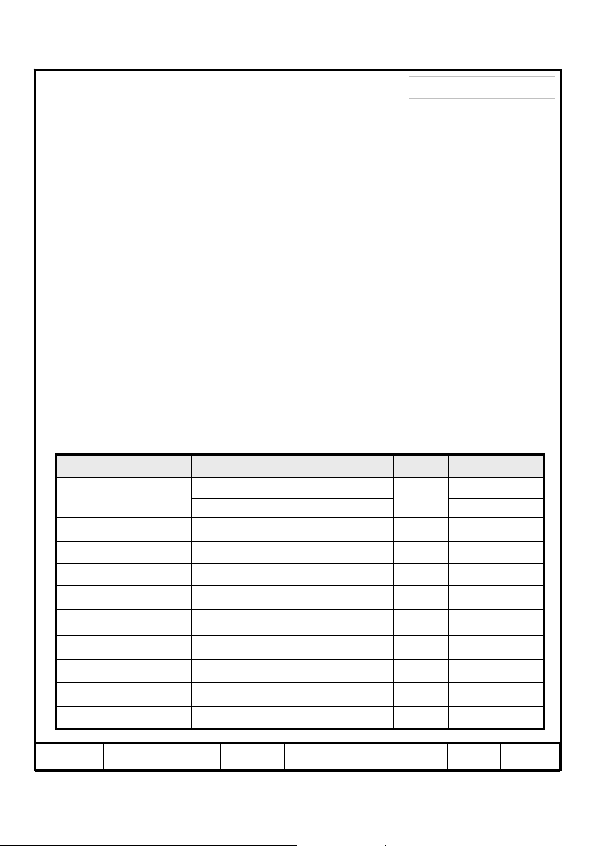
Module Size
729.6 (H) X 424.4 (V)
49.2
Haze 7% , Hard-coating(3H)Surface Treatment
RGB vertical stripePixel Arrangement
Normally BlackDisplay Mode
450 (Typ.)Luminance of White
UnitSpecificationItems
mm
g6,500 (Max)Weight
mm0.51075(H) x 0.51075(V)Pixel Pitch
mm697.6845(H) x 392.256(V)Active Display Area
colors8 bit - 16.7MDisplay Colors
pixel1366 x 768Number of Pixels
cd/m
Note
±1.0mm
2
3/ 25Page06-000-G-100105Doc. NoLTA320AP11MODEL
Page 4
Samsung Secret
Samsung Secret
1. Absolute Maximum Ratings
If the condition exceeds maximum ratings, it can cause malfunction or unrecoverable
damage to the device.
NoteUnitMax.Min.SymbolItem
Power Supply Voltage
Storage temperature
Operating temperature
Surface temperature
DD
STG
OPR
SUR
X,Y,Z 50
Vibration ( non - operating )
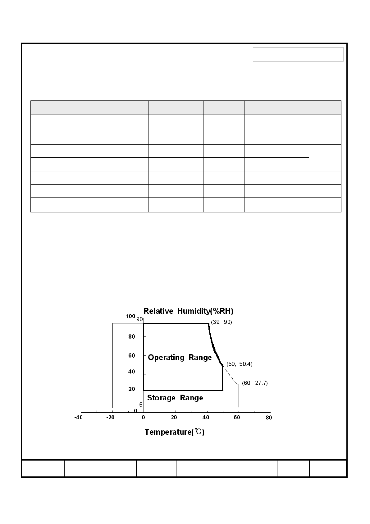
Note (1) Ta= 25 ± 2 °C
(2) Temperature and relative humidity range are shown in the figure below.
a. 90 % RH Max. (Ta ≤ 39 °C)
b. Relative Humidity is 90% or less. (Ta >39 °C)
c. No condensation
(3) Although abnormal visual problems can be occurred in T
is not damaged in this range.
(4) 11ms, sine wave, one time for ±X, ±Y, ±Z axis
(5) 10-300 Hz, Sweep rate 10min, 30min for X,Y,Z axis
NOP
SUR
V13.2GND-0.5V
V5-Max. LumDimming Control
60-20T
500T
600T
range, the polarizer
℃
℃
℃
(1)
(2)
(3)
(4)G-Shock ( non - operating )
(5)G1.5-V
Fig. Temperature and Relative humidity range
4/ 25Page06-000-G-100105Doc. NoLTA320AP11MODEL
Page 5
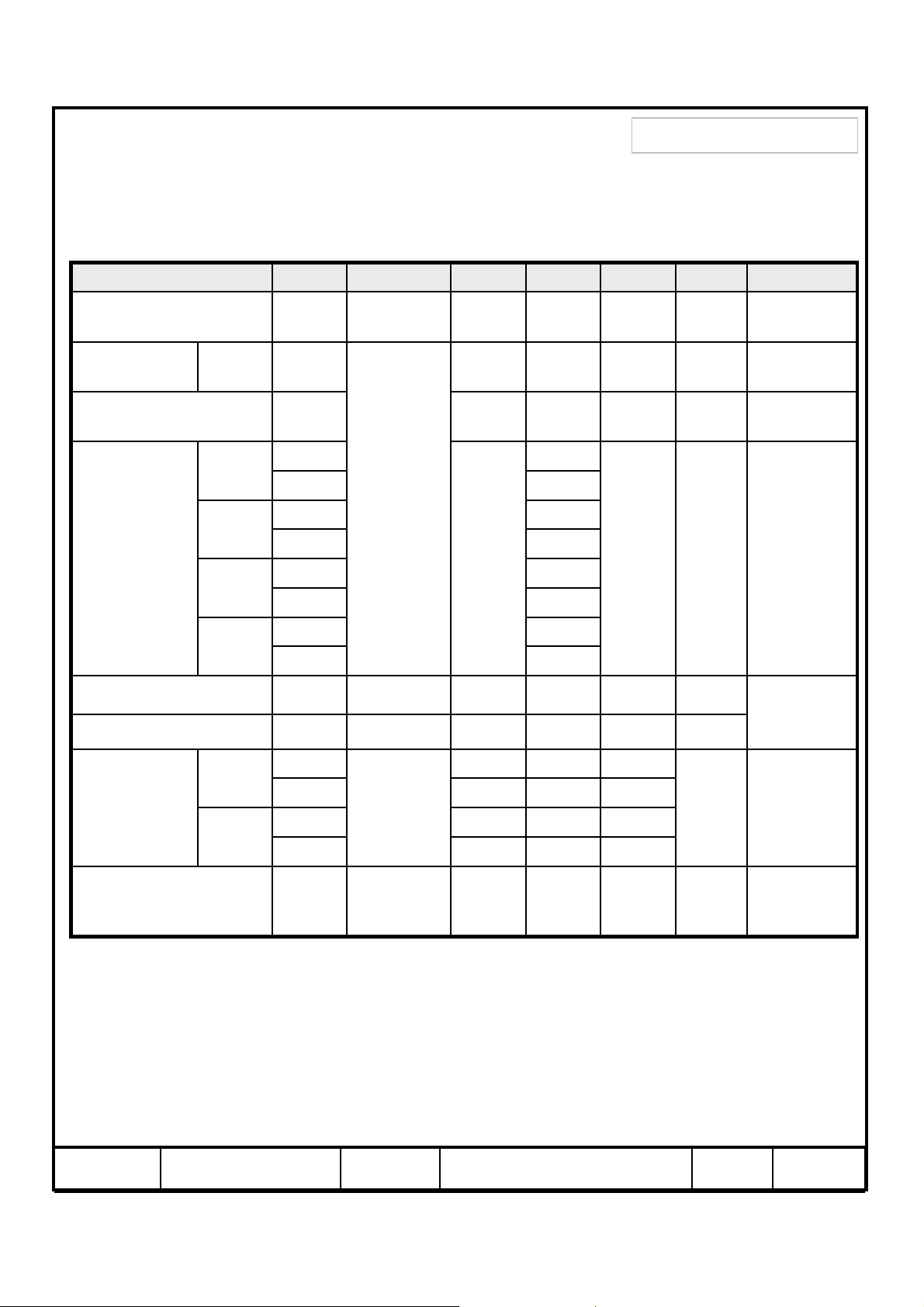
2. Optical Characteristics
The optical characteristics should be measured in a dark room or equivalent.
Measuring equipment : TOPCON RD-80S, TOPCON SR-3, ELDIM EZ-Contrast
Samsung Secret
Samsung Secret
Contrast Ratio
(Center of screen)
Response
Time
Luminance of White
(Center of screen)
Color
Green
Chromaticity
(CIE 1931)
White
(Ta = 25 ± 2°C, VDD=12V, fv= 60Hz, f
L
Red
Rx
Normal
qL,R =0
qU,D =0
Viewing
Angle
TYP.
-0.03
Blue
= 78MHz, Lamp Current = 12.5 mA)
DCLK
-4,0003,000C/R
168-TgG-to-G
-420370Y
msec
cd/m
2
TBD
TBDRy
TBDGx
TBDGy
TBDBx
TYP.
+0.03
TBDBy
0.280Wx
0.290Wy
NoteUnitMax.Typ.Min.ConditionSymbolItem
(1)
SR-3
(3)
RD-80S
(4)
SR-3
(5),(6)
SR-3
Hor.
Viewing
Angle
Ver.
White Brightness
Uniformity
(9 Points)
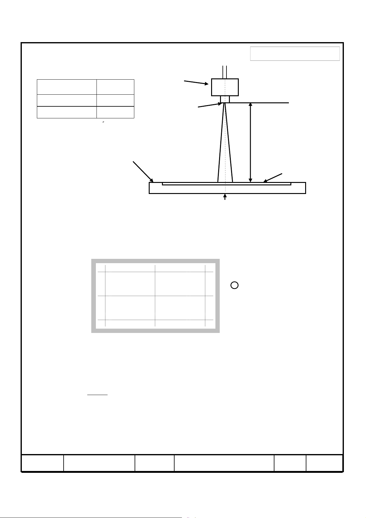
- Test Equipment Setup
The measurement should be executed in a stable, windless and dark room between
40min and 60min after lighting the back light at the given temperature for stabilization
of the back light. This should be measured in the center of screen.
Environment condition : Ta = 25 ± 2 °C
%-72--Color Gamut
K-10,000--Color Temperature
q
L
R
U
D
uni
C/R≥10
-8975
-8975q
Degree
-8975q
-8975q
%25--B
(5)
SR-3
(6)
EZ-Contrast
(2)
SR-3
5/ 25Page06-000-G-100105Doc. NoLTA320AP11MODEL
Page 6
Samsung Secret
Samsung Secret
Field Photo detector
TFT - LCD Module
- Definition of test point
320 960 1600
Photo detector
2°SR-3
1°RD-80S
Field
SR-3 : 50㎝
RD-80S : 50㎝
LCD Panel
The center of the screen
180
540
900
⑨
⑥
⑧
⑤④
Note (1) Definition of Contrast Ratio (C/R)
: Ratio of gray max (Gmax) & gray min (Gmin) at the center point ⑤ of the panel
G
CR
/
max
=
G
min
Gmax : Luminance with all pixels white
Gmin : Luminance with all pixels black
⑦
①②③
Active Area
Test Point
6/ 25Page06-000-G-100105Doc. NoLTA320AP11MODEL
Page 7
Samsung Secret
Samsung Secret
Note (2) Definition of 9 points brightness uniformity (Test pattern : Full White )
Buni
BB
=∗
(max min)
100
B
−
max
Bmax : Maximum brightness
Bmin : Minimum brightness
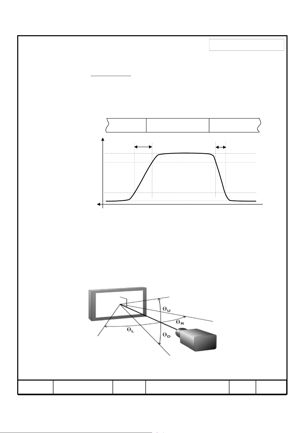
Note (3) Definition of Response time : Sum of Tr, Tf
Display data
Optical Instruments
Response
100%
90%
10%
0%
Black (data off)
T
R
White (data on)
Black (data off)
T
F
TIME
Note (4) Definition of Luminance of White : Luminance of white at center point ⑤
Note (5) Definition of Color Chromaticity (CIE 1931)
Color coordinate of Red, Green, Blue & White at center point ⑤
Note (6) Definition of Viewing Angle
: Viewing angle range (C/R ≥10)
7/ 25Page06-000-G-100105Doc. NoLTA320AP11MODEL
Page 8
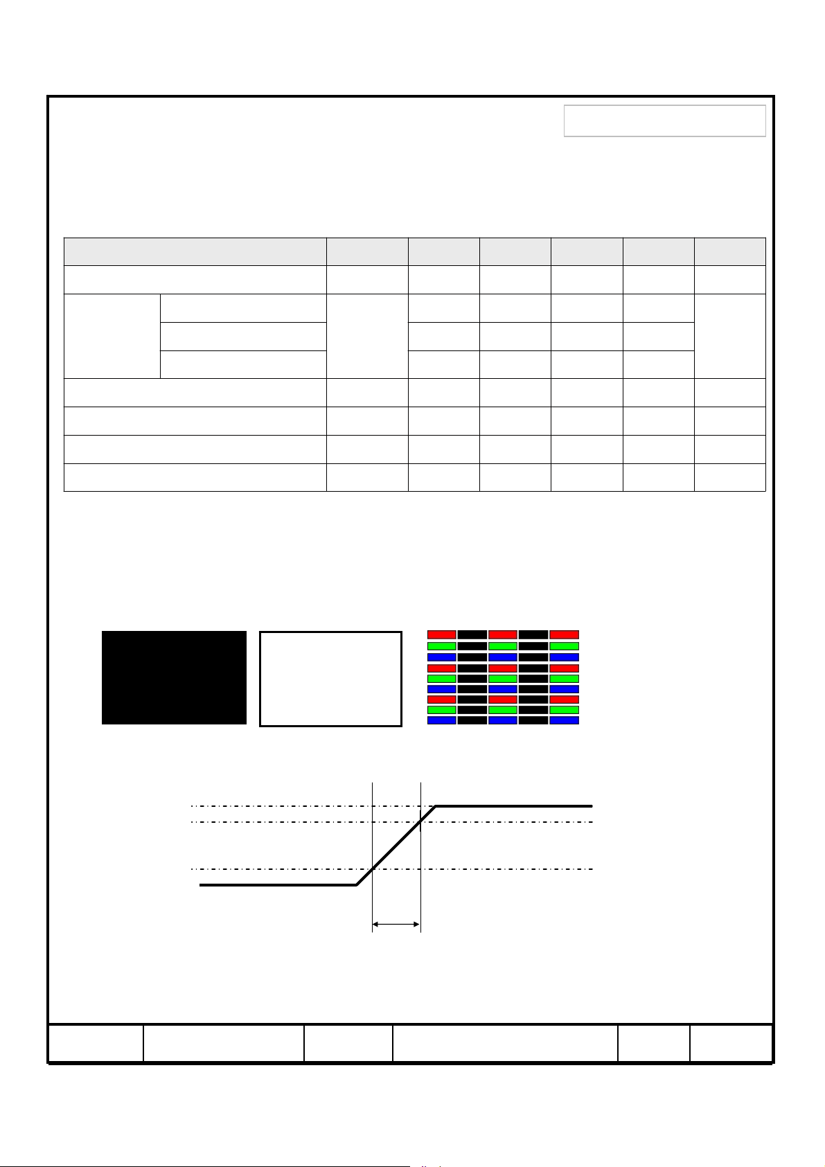
3. Electrical Characteristics
3.1 TFT LCD Module
The connector for display data & timing signal should be connected.
Samsung Secret
Samsung Secret
Ta = 25°C ± 2 °C
NoteUnitMax.Typ.Min.SymbolItem
Voltage of Power Supply
Current of
(a) Black
Power
DD
I
DD
Supply
Vsync Frequency
Hsync Frequency
Main Frequency
Rush Current
V
H
DCLK
RUSH
Note (1) The ripple voltage should be controlled under 10% of VDD.
(2) fV=60Hz, fDCLK = 78MHz, V
= 12.0V, DC Current.
DD
(3) Power dissipation check pattern (LCD Module only)
a) Black Pattern b) White Pattern c) V-STRIPE
(1)V13.212.010.8V
790590950750-(b) White
mA
mA
(2),(3)
mA1000800-(c) V-STRIPE
Hz666050f
kHz534844f
MHz857872f
(4)A4--I
(4) Measurement Conditions
100%
90%
10%
GND
Rush Current I
can be measured when T
RUSH
T
RUSH
=470㎲
. is 470㎲.
RUSH
V
DD
8/ 25Page06-000-G-100105Doc. NoLTA320AP11MODEL
Page 9
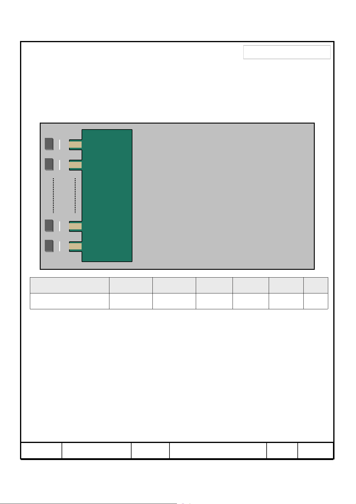
3.2 Back Light Unit
The back light unit contains 4 U-type CCFLs ( Cold Cathode Fluorescent
Lamp ). The characteristics of lamps are shown in the following tables.
Socket
HOT 1
HOT 2
LCD
Inverter
Module
Samsung Secret
Samsung Secret
Ta=25 ± 2°C
HOT 7
HOT 8
NoteUnitMax.Typ.Min.SymbolItem
(1)Hour--50,000HrOperating Life Time
Note (1) It is defined as the time to take until the brightness reduces to 50% of its original
value.
[Operating condition : Ta = 25±2℃, For single lamp only. ]
9/ 25Page06-000-G-100105Doc. NoLTA320AP11MODEL
Page 10
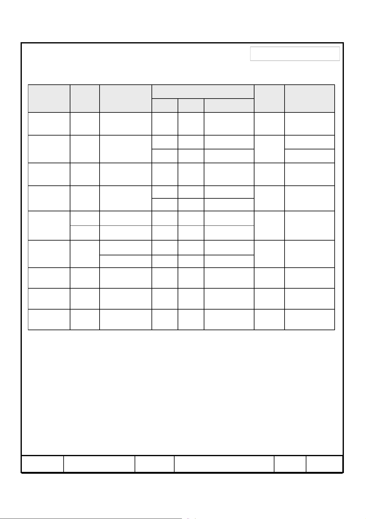
3.3 Inverter Input Condition & Specification
Samsung Secret
Samsung Secret
Items
Input
Voltage
Input
Current
Lamp
Current
Start Up
Voltage
Backlight
On/Off
Dimming
Control
Symb
ol
Conditions
Min. Typ. Max.
Specifications
Unit Note
Vin - 22 24 26 V Ta=25±2 °C
I
RUSH
I
Vin = 24V
Vdim = 3.3V
Vin = 24V
O
Vdim = 3.3V
-- 4.3
A
-TBD - (2)
12.0 12.5 13.0 mArms (2)
(1)
0℃ 2670--
S
-V
25 ℃ 2140--
-Vrms
ON Vin = 24V 2.4 - 5.5
V(3)
OFF Vin = 24V 0 - 0.8
Max Lum 3.3 - -
V
DIM
V(4)
Min. Lum - - 0
PWM Duty
PWM
Frequency
Shut-down
Time
D
F
PWM
PWM
T
SD
Vin = 24V
Dim = 0~3.3V
Vin = 24V
Dim = 0V
Vin = 24V
Dim = 3.3V
-%100-20
-Hz173166159
-Sec2.01.51.0
Note) Power Consumption is measured when 500[cd/m2] of luminance which is the typical luminance.
Lamp Current is measured at the point before Lamp.
(1) Max Value of the Power Consumption is measured during initial turn-on time* of the backlight.
(2) Max Value of the Power Consumption is measured after 120 min warm-up.
(3) Inverter pin NO.12 is for backlight On/Off.
(4) Inverter pin NO.13 is for dimming control.
* Initial turn-on time : From 0sec to 60min after turn-on
10 / 25Page06-000-G-100105Doc. NoLTA320AP11MODEL
Page 11
Samsung Secret
4. Input Terminal Pin Assignment
Samsung Secret
4.1. Input Signal & Power Connector :IS100-L30O-C23
PIN No. Description PIN No. Description
1 No Connection (Note1) 16 GND
2 No Connection (Note1) 17 RxIN33 No Connection (Note1) 18 RxIN3+
4GND19GND
5RxIN0-20No Connection (Note1)
6 RxIN0+ 21 LVDS OPTION (Note 2)
7GND22No Connection (Note1)
8RxIN1-23GND
9RxIN1+24 GND
10 GND 25 GND
11 RxIN2- 26 Vin
12 RxIN2+ 27 Vin
13 GND 28 Vin
14 RxCLK- 29 Vin
15 RxCLK+ 30 Vin
Note1) No Connection: This PINS are only used ONLY for SAMSUNG.
Note2) LVDS OPTION : If this PIN is HIGH (3.3 V) → Normal LVDS format
LOW (GND) → JEIDA LVDS format
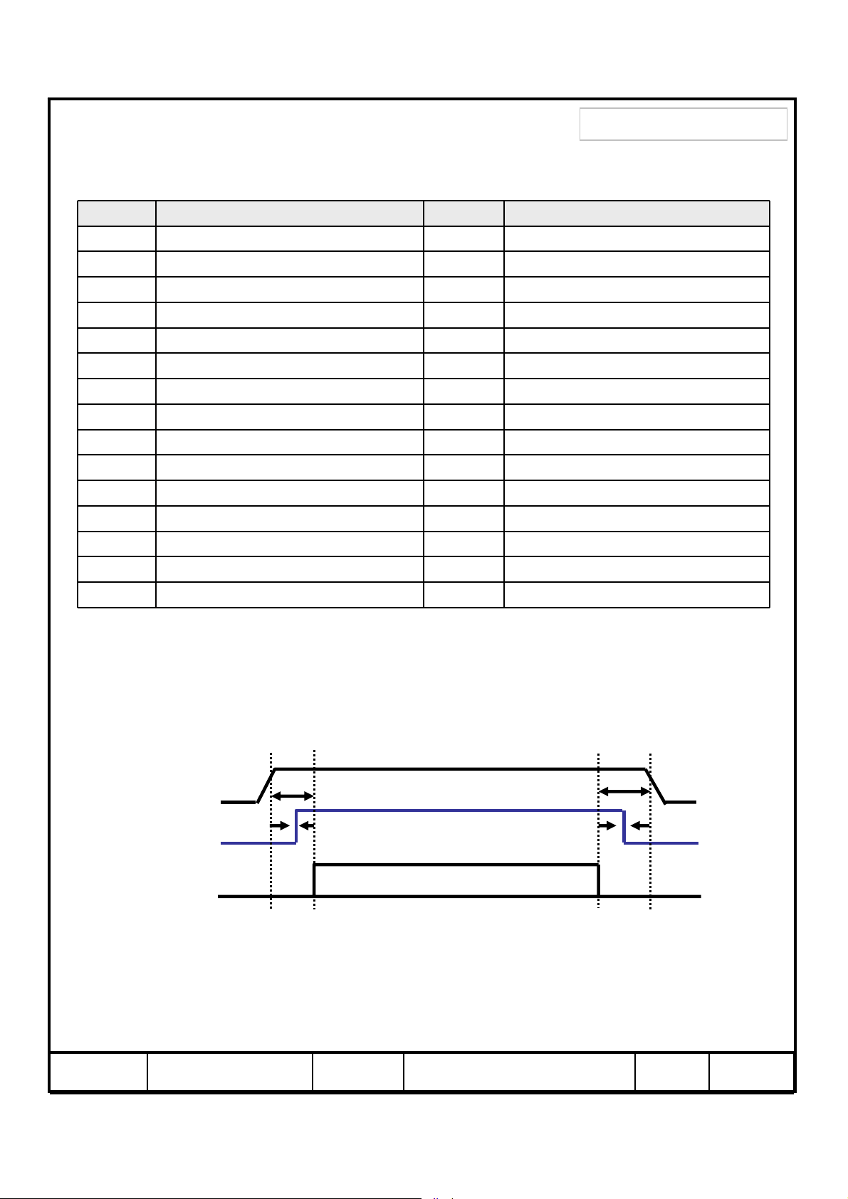
SEQUENCE : On = V
DD(T1) ≥ LVDS Option ≥ Interface Signal(T2)
OFF = Interface Signal(T3) ≥ LVDS Option ≥ V
Vin
LVDS
Option
LVDS
Signal
T2
LVDS Option Sequence
DD
T3
11 / 25Page06-000-G-100105Doc. NoLTA320AP11MODEL
Page 12
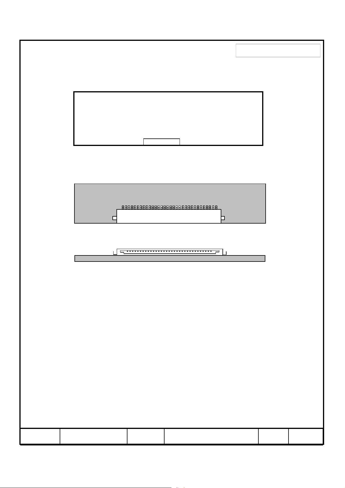
Note(1) Pin number starts from Left side
▼
Pin No. 1 Pin No. 30
#1 #30
PCB
Samsung Secret
Samsung Secret
#1
Fig. Connector diagram
a. Power GND pins should be connected to the LCD’s metal chassis.
b. All power input pins should be connected together.
c. All NC pin should be separated from other signal or power.
#30
12 / 25Page06-000-G-100105Doc. NoLTA320AP11MODEL
Page 13
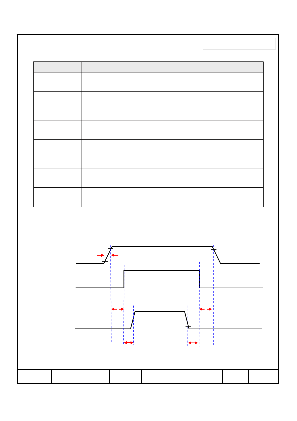
4.2 Inverter Input Pin Configuration
Connector : JST, S14B-PHA-SM-TB(LF)
Pin No. Pin Configuration (FUNCTION)
1Vin (24 V)
2Vin (24 V)
3Vin (24 V)
4Vin (24 V)
5Vin (24 V)
6GND
7GND
8GND
9GND
10 GND
11 No Connection (DO NOT CONNECT)
12 Backlight On /Off [ON: 2.4 ~ 5.5 V, OFF: 0 ~ 0.8 V]
Samsung Secret
Samsung Secret
13 Dimming Control [ 0V : Min, 3.3V: Max ]
14 No Connection (DO NOT CONNECT)
4.3. Inverter Input Power Sequence
0.9 Vin
Vin (24V)
Dimming Control
( 0 ~ 3.3 V )
0.5sec [Min]
Backlight On/Off
0.1 Vin
20msec [Min]
0.9 Vin
0.5sec [Min]
2.4V(On level)
0.8V(Off level)
0.5sec [Min]
0.1sec [Min]
13 / 25Page06-000-G-100105Doc. NoLTA320AP11MODEL
Page 14
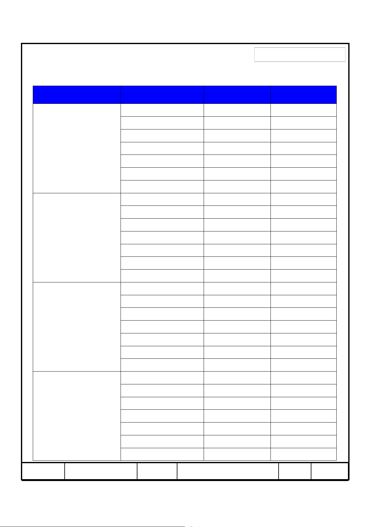
4.4 LVDS Interface
- LVDS Receiver : Tcon (merged)
- Data Format (JEIDA & VESA)
TxIN/RxOUT0 R2 R0
TxIN/RxOUT1 R3 R1
TxIN/RxOUT2 R4 R2
Samsung Secret
Samsung Secret
LVDS pin JEIDA -DATA VESA -DATA
TxOUT/RxIN0
TxOUT/RxIN1
TxOUT/RxIN2
TxIN/RxOUT3 R5 R3
TxIN/RxOUT4 R6 R4
TxIN/RxOUT6 R7 R5
TxIN/RxOUT7 G2 G0
TxIN/RxOUT8 G3 G1
TxIN/RxOUT9 G4 G2
TxIN/RxOUT12 G5 G3
TxIN/RxOUT13 G6 G4
TxIN/RxOUT14 G7 G5
TxIN/RxOUT15 B2 B0
TxIN/RxOUT18 B3 B1
TxIN/RxOUT19 B4 B2
TxIN/RxOUT20 B5 B3
TxIN/RxOUT21 B6 B4
TxIN/RxOUT22 B7 B5
TxOUT/RxIN3
TxIN/RxOUT24 HSYNC HSYNC
TxIN/RxOUT25 VSYNC VSYNC
TxIN/RxOUT26 DEN DEN
TxIN/RxOUT27 R0 R6
TxIN/RxOUT5 R1 R7
TxIN/RxOUT10 G0 G6
TxIN/RxOUT11 G1 G7
TxIN/RxOUT16 B0 B6
TxIN/RxOUT17 B1 B7
TxIN/RxOUT23 RESERVED RESERVED
14 / 25Page06-000-G-100105Doc. NoLTA320AP11MODEL
Page 15
Samsung Secret
Samsung Secret
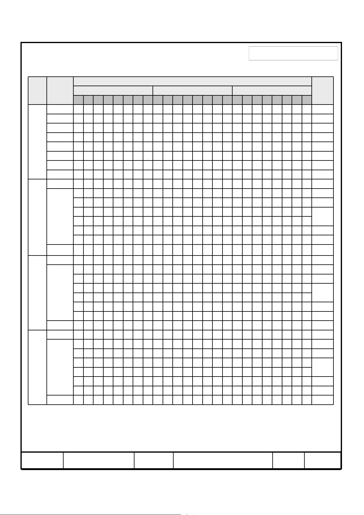
4.5 Input Signals, Basic Display Colors and Gray Scale of Each Color
COLOR
BASIC
COLOR
GRAY
SCALE
OF
RED
GRAY
SCALE
OF
GREEN
GRAY
SCALE
OF
BLUE
DATA SIGNAL
DISPLAY
(8bit)
R0 R1 R2 R3 R4 R5 R6 R7 G0 G1 G2 G3 G4 G5 G6 G7 B0 B1 B2 B3 B4 B5 B6 B7
BLACK 000000000000000000000000 -
BLUE 000000000000000011111111 -
GREEN 000000001111111100000000 -
CYAN 000000001111111111111111 -
RED 111111110000000000000000 -
MAGENTA111111110000000011111111 -
YELLOW111111111111111100000000 -
WHITE 111111111111111111111111 BLACK 000000000000000000000000 R0
100000000000000000000000 R1
DARK
↑
↓
LIGHT
RED 111111110000000000000000 R255
BLACK 000000000000000000000000 G0
DARK
↑
↓
LIGHT
GREEN 000000001111111100000000 G255
BLACK 000000000000000000000000 B0
DARK
↑
↓
LIGHT
BLUE 000000000000000011111111 B255
010000000000000000000000 R2
:::::: :::::: ::::::
:::::: :::::: ::::::
101111110000000000000000 R253
011111110000000000000000 R254
000000001000000000000000 G1
000000000100000000000000 G2
:::::: :::::: ::::::
:::::: :::::: ::::::
000000001011111100000000 G253
000000000111111100000000 G254
000000000000000010000000 B1
000000000000000001000000 B2
:::::: :::::: ::::::
:::::: :::::: ::::::
000000000000000010111111 B253
000000000000000001111111 B254
RED GREEN BLUE
GRAY
SCALE
LEVEL
R3~
R252
G3~
G252
B3~
B252
Note) Definition of Gray :
Rn : Red Gray, Gn : Green Gray, Bn : Blue Gray (n = Gray level)
Input Signal : 0 = Low level voltage, 1 = High level voltage
15 / 25Page06-000-G-100105Doc. NoLTA320AP11MODEL
Page 16
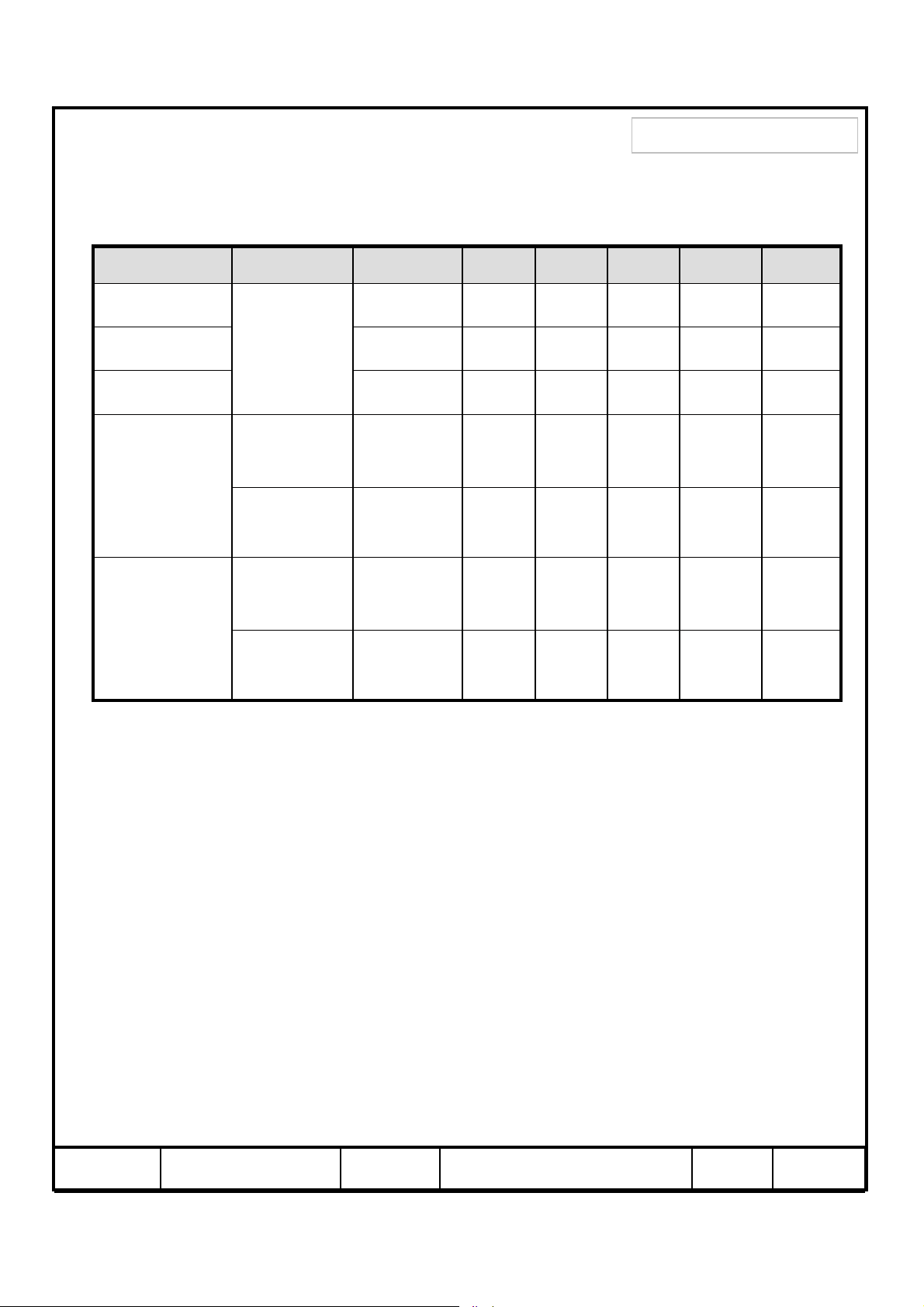
5. Interface Timing
5.1 Timing Parameters ( DE mode )
Samsung Secret
Samsung Secret
NOTEUnitMAX.TYP.MIN.SYMBOLITEMSIGNAL
Clock
Hsync
Vsync
Frequency
C
H
V
Active
Vertical
Display
Period
VD
Display Term
Vertical
Total
V
Active
Horizontal
Display
Period
HD
Display Term
Horizontal
Total
H
Note) This product is DE mode. But the Hsync & Vsync signal must be inputted
-MHz8578721/T
-KHz534844F
-Hz666050F
-Lines-768-T
-Lines1200802773T
-Clocks-1366-T
-clocks200016241460T
(1) Test Point : TTL control signal and CLK at LVDS Tx input terminal in system
(2) Internal VDD = 3.3V
(3) Spread spectrum
- Modulation rate (max) : ± 1.5 %
- Modulation Frequency : under 100KHz
16 / 25Page06-000-G-100105Doc. NoLTA320AP11MODEL
Page 17
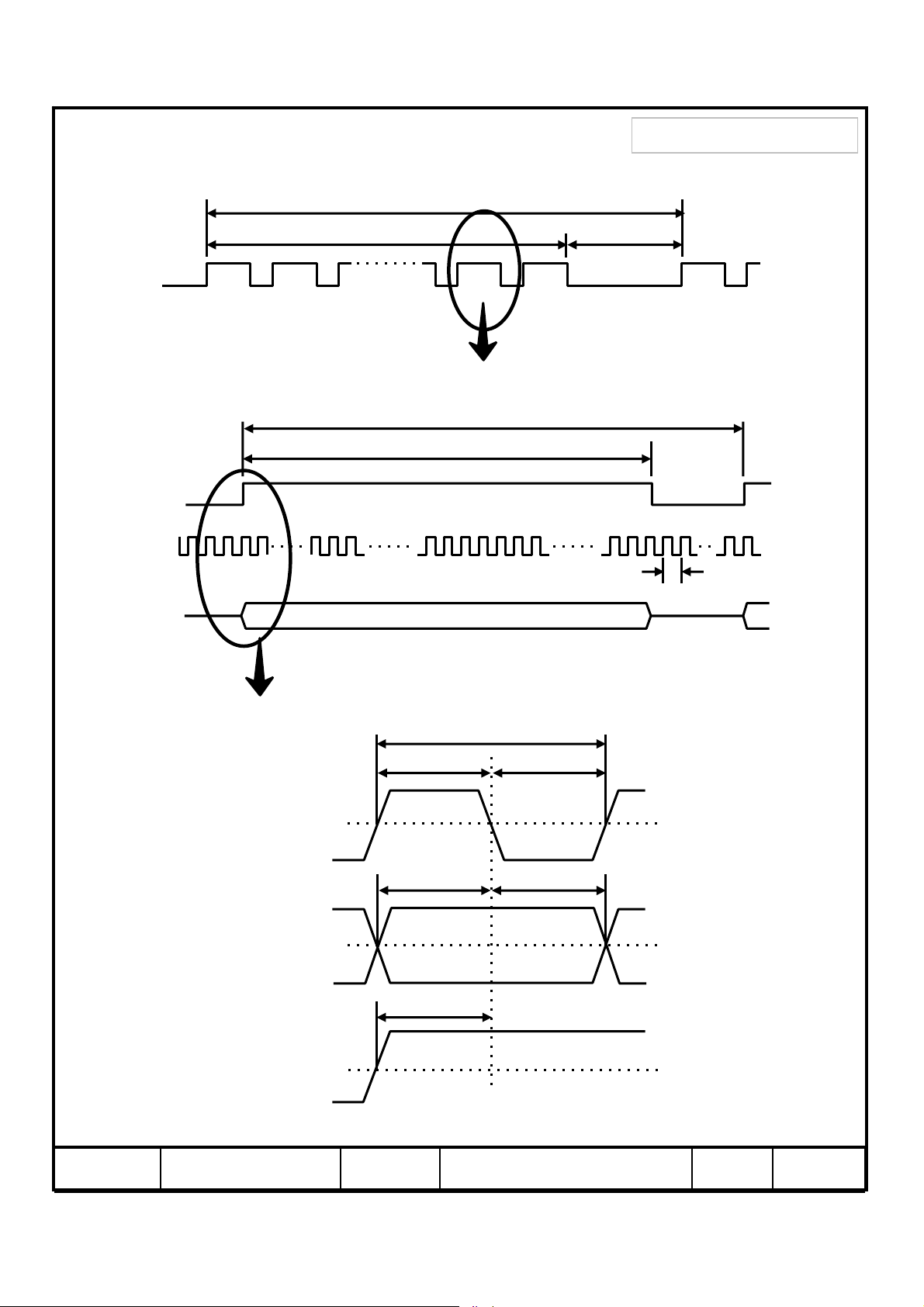
5.2 Timing diagrams of interface signal ( DE mode )
TV
Samsung Secret
Samsung Secret
DE
DE
DCLK
DATA
SIGNALS
TVD
TVB
TH
THD
TC
DCLK
DISPLAY
DATA
DE
TC
TCH
TDS TDH
TES
TCL
0.5
V
0.5
V
CC
0.5
V
CC
CC
17 / 25Page06-000-G-100105Doc. NoLTA320AP11MODEL
Page 18
Samsung Secret
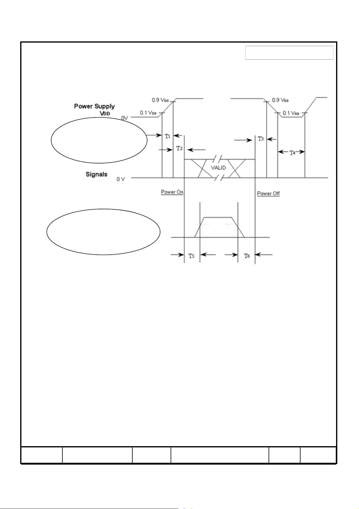
5.3 Power ON/OFF Sequence
Samsung Secret
To prevent a latch-up or DC operation of the LCD Module, the power on/off
sequence should be as the diagram below.
2msec<T1≤10msec
0<T2≤50msec
0<T3≤50msec
1000msec≤T4
1000msec≤T5
(Recommend Value)
100msec≤T6
(Recommend Value)
0.5 Vcc
T1 : VDDrising time from 10% to 90%
T2 : The time from V
T3 : The time from valid data off to V
T4 : V
off time for Windows restart
DD
to valid data at power ON.
DD
off at power Off.
DD
T5 : The time from valid data to B/L enable at power ON.
T6 : The time from valid data off to B/L disable at power Off.
The supply voltage of the external system for the Module input should be the same
as the definition of V
DD
.
Apply the lamp voltage within the LCD operation range. When the back light turns on
before the LCD operation or the LCD turns off before the back light turns off,
the display may momentarily show abnormal screen.
In case of V
= off level,
DD
please keep the level of input signals low or keep a high impedance.
T4 should be measured after the Module has been fully discharged between power off
and on period.
Interface signal should not be kept at high impedance when the power is on.
In Case T5 is less than 1000msec and T6 is less than 100msec,
Garbage Display can be seen. (It is not related to electrical function issue, Just for
recommendation to prevent Garbage Display )
18 / 25Page06-000-G-100105Doc. NoLTA320AP11MODEL
Page 19
6. Outline Dimension- Front
Samsung Secret
Samsung Secret
TBD
19 / 25Page06-000-G-100105Doc. NoLTA320AP11MODEL
Page 20
6. Outline Dimension- Rear
Samsung Secret
Samsung Secret
TBD
20 / 25Page06-000-G-100105Doc. NoLTA320AP11MODEL
Page 21
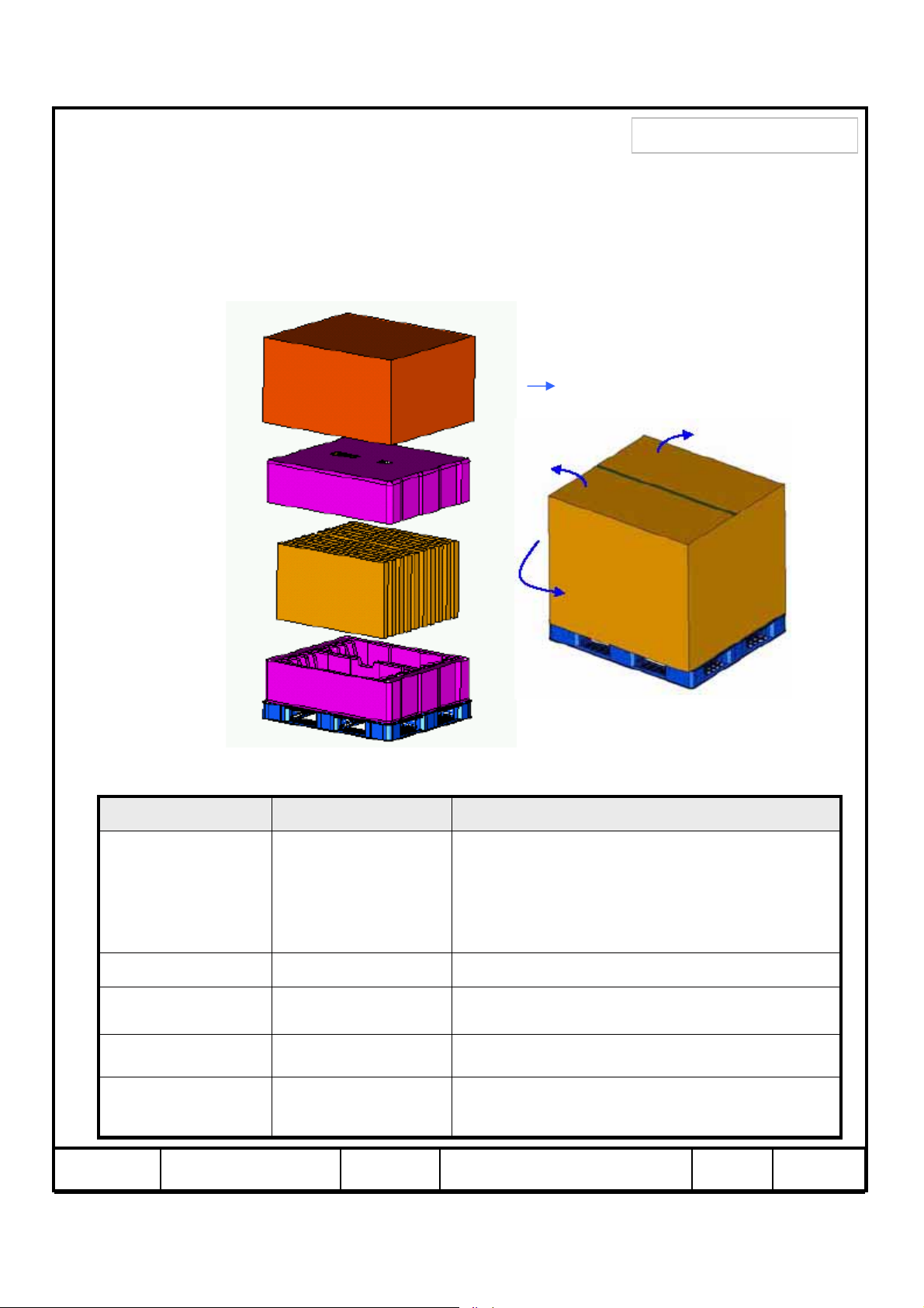
7. PACKING
7.1 CARTON (Internal Package)
(1) Packing Form
Corrugated fiberboard box and corrugated cardboard as shock absorber
(2) Packing Method
Packing
-Pallet Box
Cushion-Foam
LCD Module
Samsung Secret
Samsung Secret
Direction be able to open it
Cushion-Foam
Pallet-Plastic
7.2 Packing Specification
LCD Packing
Total Pallet
Weight
24ea / (Packing-
Pallet Box)
1Box / PalletPallet
H x V x heightTotal Pallet Size
VerticalPac k i ng Direc tion
168 kg
RemarkSpecificationItem
1. 144 Kg / LCD (24ea)
2. 14 Kg / Cushion-cover (4ea)
3.2.0 Kg / Packing-Pallet Box (1ea)
4. Cushion-pallet Material : EPS
5. Packing-Pallet Box Material : DW4
1. Pallet weight = 8kg
1150mm(H) x 985mm(V) x 1161mm(height)
Pallet(2kg) + Module(6kg*24ea=144kg) +
Cushion(3.5kg*4ea=14kg) + Pallet-BOX(8.0kg)
21 / 25Page06-000-G-100105Doc. NoLTA320AP11MODEL
Page 22
Samsung Secret
Samsung Secret
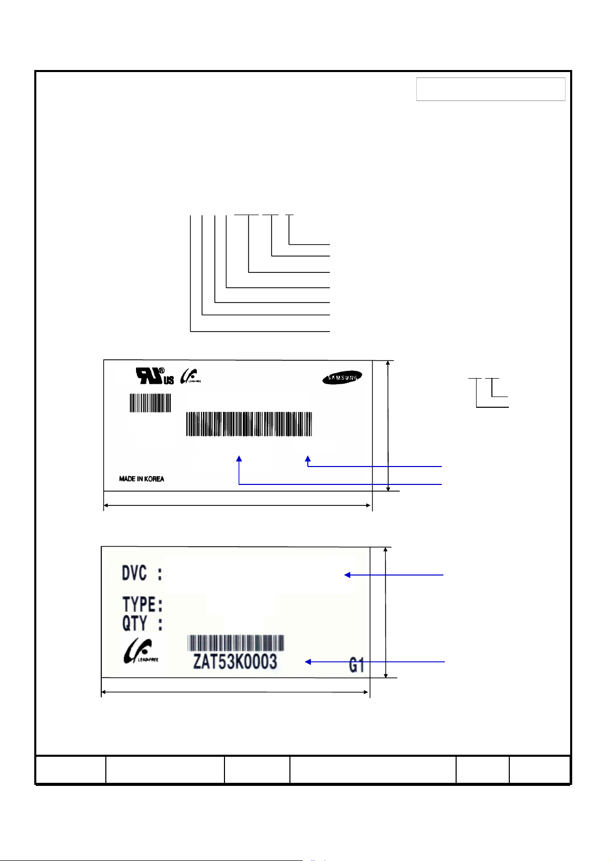
8. MARKING & OTHERS
A nameplate bearing followed by is affixed to a shipped product at the specified
location on each product.
(1) Part number : LTA320AP11
(2) Revision: Three letters
(3) Lot number : X X X X XXX XX X
Cell Position No. (In the Glass)
Glass No. (In the one Lot)
Lot No. (Glass)
Month
Year (Note1)
Product code
Line
(4) Nameplate Indication
T
C
LTA320AP11
0925
XXXX
(5) Packing box attach
XXXXXXXXXX XXX
LTA320AP11
Week code : 09 25
week
year
40mm
Revision code
Lot number
80mm
100mm
Part number
XXX
22
Box serial number
165mm
(6) Others
1. After service part
Lamps cannot be replaced because of the narrow bezel structure.
22 / 25Page06-000-G-100105Doc. NoLTA320AP11MODEL
Page 23
Samsung Secret
9. General Precautions
Samsung Secret
9.1 Handling
(a) When the Module is assembled, it should be attached to the system firmly
using all mounting holes. Be careful not to twist and bend the Module.
(b) Because the inverter use high voltage, it should be disconnected from power
before it is assembled or disassembled.
(c) Refrain from strong mechanical shock and / or any force to the Module.
In addition to damage, this may cause improper operation or damage to the Module
and CCFT back light.
(d) Note that polarizers are very fragile and could be damage easily.
Do not press or scratch the surface harder than a HB pencil lead.
(e) Wipe off water droplets or oil immediately. If you leave the droplets for a long
time, staining or discoloration may occur.
(f) If the surface of the polarizer is dirty, clean it using absorbent cotton or soft cloth.
(g) Desirable cleaners are water, IPA(Isopropyl Alcohol) or Hexane.
Do not use Ketone type materials(ex. Acetone), Ethyl alcohol, Toluene, Ethyl acid
or Methyl chloride. It might permanent damage to the polarizer due to chemical
reaction.
(h) If the liquid crystal material leaks from the panel, it should be kept away
from the eyes or mouth . In case of contact with hands, legs or clothes, it must
be washed away with soap thoroughly.
(i) Protect the module from Electrostatic discharge. Otherwise the ASIC IC or
semiconductor would be damaged.
(j) Use finger-stalls with soft gloves in order to keep display clean during the
incoming inspection and assembly process.
(k) Do not disassemble the Module.
(l) Do not disassemble shield case of inverter & LVDS board
(m) Do not connect N.C pins. (Samsung internal use only)
(n) Protection film for polarizer on the Module should be slowly peeled off just before use
so that the electrostatic charge can be minimized. Must put on antistatic glove while
handling a module
(o) Pins of I/F connector should not be touched directly with bare hands.
23 / 25Page06-000-G-100105Doc. NoLTA320AP11MODEL
Page 24
Samsung Secret
Samsung Secret
9.2 Storage
(a) Do not leave the Module in high temperature, and high humidity for a long time.
It is highly recommended to store the Module with temperature from 0 to 35℃
and relative humidity of less than 70%.
(b) Do not store the TFT- L CD Module in direct sunlight.
(c) The Module should be stored in a dark place. It is prohibited to apply sunlight or
fluorescent light in storing.
9.3 Operation
(a) Do not connect or disconnect the Module in the "Power On" condition.
(b) Power supply should always be turned on/off by the "Power on/off sequence"
(c) Module has high frequency circuits. Sufficient suppression to the electromagnetic
interference should be done by system manufacturers. Grounding and shielding methods
may be important to minimize the interference.
(d) The cable between the back light connector and its inverter power supply should
be connected directly with a minimized length. A longer cable between
the back light and the inverter may cause lower luminance of lamp(CCFT) and
may require higher startup voltage(Vs).
9.4 Operation Condition Guide
(a) The LCD product should be operated under normal conditions.
Normal condition is defined as below;
- Temperature : 20±15℃
- Humidity : 55±20%
- Display pattern : continually changing pattern (Not stationary )
(b) If the product will be used in extreme conditions such as high temperature,
humidity, display patterns or operation time etc.., It is strongly recommended
to contact SEC for Application engineering advice. Other wise, its reliability and
function may not be guaranteed. Extreme conditions are commonly found at
Airports, Transit Stations, Banks, Stock market, and Controlling systems.
24 / 25Page06-000-G-100105Doc. NoLTA320AP11MODEL
Page 25
Samsung Secret
9.5 Others
(a) Ultra-violet ray filter is necessary for outdoor operation.
(b) Avoid condensation of water. It may result in improper operation or disconnection
of electrode.
(c) Do not exceed the absolute maximum rating value. ( supply voltage variation,
input voltage variation, variation in part contents and environmental temperature,
and so on)
Otherwise the Module may be damaged.
(d) If the Module keeps displaying the same pattern for a long period of time,
the image may be "sticked" to the screen.
To avoid image sticking, it is recommended to use a screen saver.
(e) This Module has its circuitry PCB's on the rear side and should be handled
carefully in order not to be stressed.
(f) Please contact SEC in advance when you display the same pattern for a long time.
Samsung Secret
25 / 25Page06-000-G-100105Doc. NoLTA320AP11MODEL
 Loading...