

Page 1
CUSTOMER
CT Frank
MODEL NO.
LSC400HM06
DATE OF ISSUE
2013/4/4
EXTENSION CODE
T
LCD Sales & Marketing Team
Samsung Display Co., Ltd
Product Specification
( √ ) Preliminary Specification
( ) Approval Specification
The information described in this specification is preliminary and can be
changed without prior notice.
Page 2

————————————————————————————————————————————————–
Table of Contents
REVISION HISTORY .......................................................................................................................................................... 3
1. GENERAL DESCRIPTION ............................................................................................................................................. 4
2. ABSOLUTE MAXIMUM RATINGS.............................................................................................................................. 5
3. OPTICAL CHARACTERISTICS ..................................................................................................................................... 6
4. ELECTRICAL CHARACTERISTICS ............................................................................................................................... 9
4.1 TFT LCD MODULE ..................................................................................................................................................... 9
5. INPUT TERMINAL PIN ASSIGNMENT .................................................................................................................... 10
5.1 INPUT SIGNAL & POWER ....................................................................................................................................... 10
5.2 LVDS INTERFACE ..................................................................................................................................................... 13
5.3 INPUT COLOR DATA MAPPING............................................................................................................................. 14
6. INTERFACE TIMING ................................................................................................................................................... 15
6.1 TIMING PARAMETERS OF TIMING (ONLY DE MODE) ............................................................................................ 15
6.2 TIMING DIAGRAMS OF INTERFACE SIGNAL ........................................................................................................ 15
6.3 CHARACTREISTICS OF INPUT DATA OF LVDS ..................................................................................................... 16
6.4 POWER ON/OFF SEQUENCE ................................................................................................................................. 17
7. OUTLINE DIMENSION ............................................................................................................................................... 18
8. PACKING ...................................................................................................................................................................... 19
8.1 CARTON................................................................................................................................................................... 19
8.2 MARKING ................................................................................................................................................................ 20
9. GENERAL PRECAUTIONS .......................................................................................................................................... 22
9.1 HANDLING .............................................................................................................................................................. 22
9.2 STORAGE ................................................................................................................................................................. 24
9.3 OPERATION ............................................................................................................................................................. 24
9.4 OPERATION CONDITION GUIDE................................................................ ................................ ........................... 25
9.5 PROCESS EXECUTING GUIDE................................................................................................................................. 25
9.6 OTHERS .................................................................................................................................................................... 26
10. SPECIAL PRECAUSTIONS........................................................................................................................................ 27
APPENDIX – RECOMMENDATION FOR THE BLU DESIGN .................................................................................... 28
——————————————————————————————————————————————––—
Doc.No. LSC400HM06-T Page 2 of 37 Rev.No. 06-000-G-20130404
Page 3

————————————————————————————————————————————————–
Date.
Rev.No.
Page
Revision Description
2013/4/4
000 Initial Release
For eyes of CT Frank only
REVISION HISTORY
——————————————————————————————————————————————––—
Doc.No. LSC400HM06-T Page 3 of 37 Rev.No. 06-000-G-20130404
Page 4
————————————————————————————————————————————————–
Item
Specification
Unit
Note
Active Display Area
885.60 (H) x 498.15 (V)
mm
Switching Components
a-Si TFT Active matrix
Glass size
TFT :906.40H) x 518.00(V)
CF : 906.40(H) x 515.26(V)
mm
±0.5mm
Panel Size
906.40(H) x 518.00(V)
mm
±0.5mm
1.80(D)
mm
±0.1mm
Weight
2090 (Max)
g Display Colors
1.07B (Dithered 10bit )
Number of Pixels
1920 × 1080
16:9
Pixel Arrangement
RGB Horizontal Stripe
mm
Display Mode
Normally Black
Surface Treatment
Anti Glare
For eyes of CT Frank only
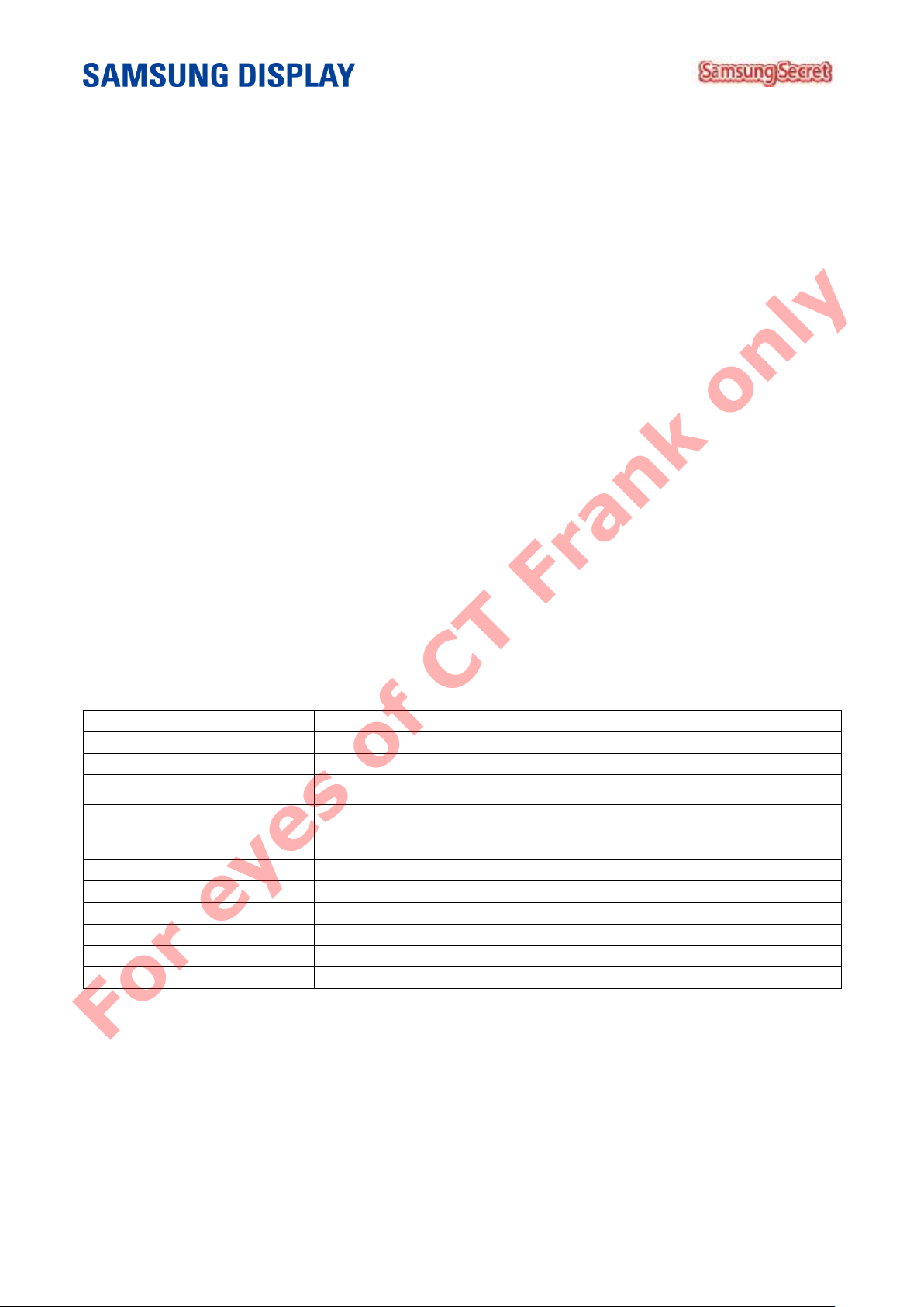
1. GENERAL DESCRIPTION
DESCRIPTION
This model uses a liquid crystal display (LCD) of amorphous silicon TFT as switching components. This model is
composed of a TFT LCD panel, a driver circuit, and an ass’y KIT of source PBA. This 40.0” model has a
resolution of a 1920 x 1080 and can display up to 1.07 Billion colors with the wide viewing angle of 89° or a
higher degree in all directions. This panel is designed to support applications by providing a excellent
performance function of the flat panel display such as home-alone multimedia TFT-LCD TV and a high
definition TV.
FEATURES
RoHS compliance (Pb-free)
High contrast ratio & aperture ratio with the wide color gamut
S-PVA (Super Patterned vertical align) mode
Wide viewing angle (± 89°)
High speed response
FHD resolution (1920 x 1080, 16:9)
DE (Data enable) mode
The interface (2Pixel/clock) of 2ch LVDS (Low voltage differential signaling)
GENERAL INFORMATION
——————————————————————————————————————————————––—
Doc.No. LSC400HM06-T Page 4 of 37 Rev.No. 06-000-G-20130404
Page 5
————————————————————————————————————————————————–
Item
Symbol
Min.
Max.
Unit
Note
Power supply voltage
VDD
10.8
13.2
V
(1)
Temperature for storage
(Temperature of glass surface)
T
STG
-20
60
C
(2), (4)
Humidity for storage
H
STG
5
90
%RH
Operating temperature
T
OPR
0
50
C
(2), (5)
Operating humidity
H
STG
20
90
%RH
Endurance on static electricity
150 V (3)
Fig. Range for temperature and relative humidity (unpacking condition)
For eyes of CT Frank only
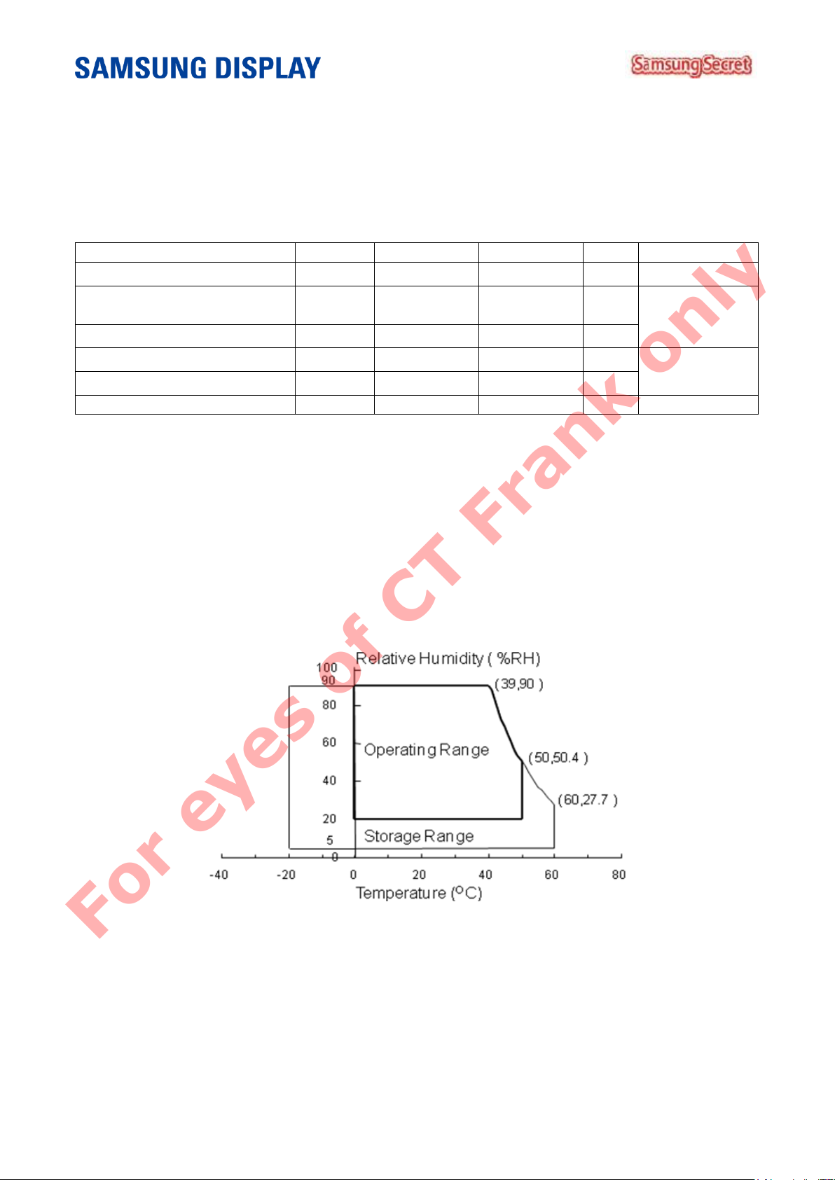
2. ABSOLUTE MAXIMUM RATINGS
If the figures on measuring instruments exceed maximum ratings, it can cause the malfunction or the
unrecoverable damage on the device.
Note (1) The power supply voltage at Ta= 25 ± 2 °C
(2) Temperature and the range of relative humidity are shown in the figure below.
a. 90 % RH Max. (Ta ≤ 39 °C)
b. The relative humidity is 90% or less. (Ta >39 °C)
c. No condensation
(3) Keep the static electricity under 150V in process the polarizer is attached on glass.
(4) Storage condition with glass.
(5) Operating condition with assembly
(6) Condition without packing.(Unpacking condition)
——————————————————————————————————————————————––—
Doc.No. LSC400HM06-T Page 5 of 37 Rev.No. 06-000-G-20130404
Page 6
————————————————————————————————————————————————–
Item
Symbol
Condition
Min.
Typ.
Max.
Unit
Note
Contrast Ratio
CR
3000
5000
-
-
(1)
SR-3
Response time
G-to-G
Tg - 8 16
msec
(2)
RD-80S
Luminance of white
(At the center of screen))
YL
280
340
-
cd/m2
(3)
SR-3
Color
Chromaticity
(CIE)
Red
RX
Normal
qL,R=0
qU,D=0
Viewing
Angle
TYP
-0.03
0.660
TYP
+0.03
(4),(5)
SR-3
RY
0.330
Green
GX
0.265
GY
0.590
Blue
BX
0.135
BY
0.120
White
WX
0.295
WY
0.365
Viewing
Angle
Hor.
q
CR 10
At center
75
89
-
Degrees
(5)
SR-3
EZ-Contrast
q
75
89
-
Ver.
q
75
89
-
q
75
89
-
Color Gamut
67
69 - %
Color
5000
7000
-
K
For eyes of CT Frank only
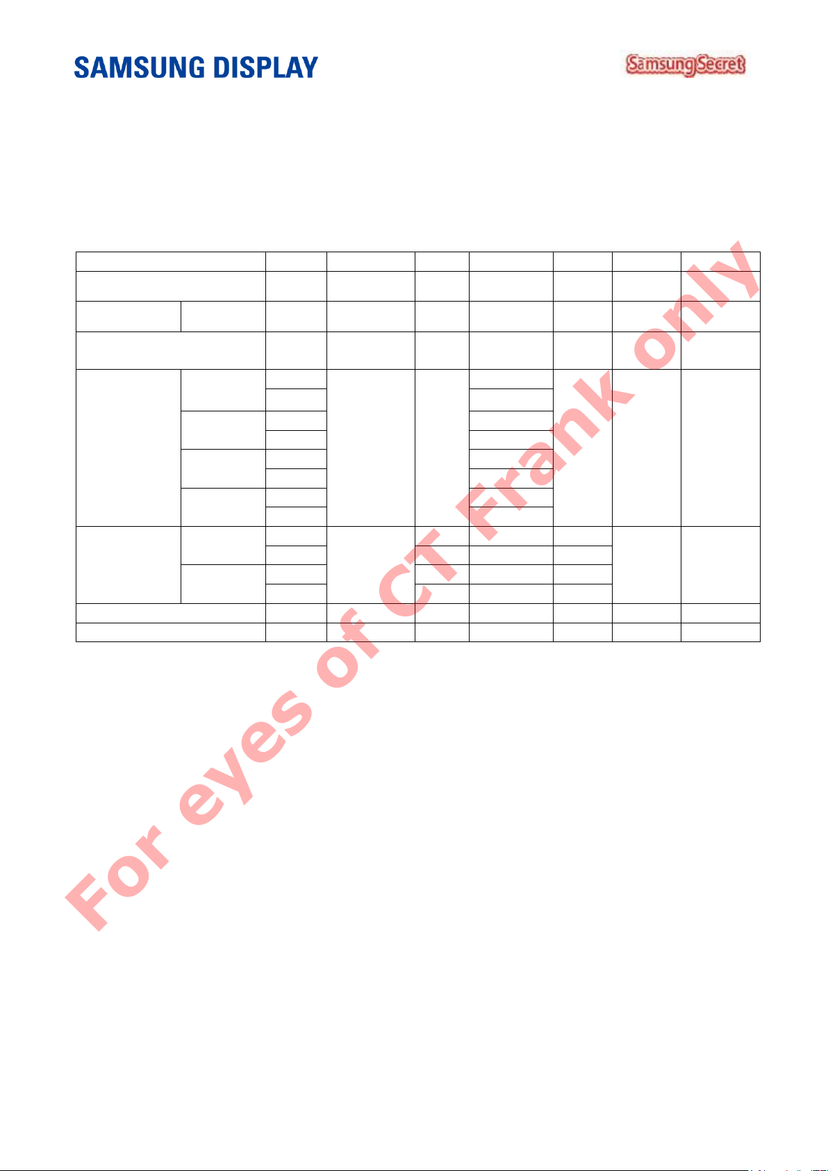
3. OPTICAL CHARACTERISTICS
The optical characteristics should be measured in the dark room or the space surrounded by the similar
setting. Measuring equipment : TOPCON RD-80S, TOPCON SR-3 ,ELDIM EZ-Contrast
Ta = 25 ± 2°C, VDD=12.0V, fv=60Hz, fDCLK=148.5MHz, Light source: D65 Standard Light
Notice
(a) Setup for test equipment
The measurement should be executed in a stable, windless, and dark room for 40min and 60min after
operating the panel at the given temperature for stabilization of the standard light. (SDC uses the standard
luminance of the D65media).
This measurement should be measured at the center of screen.
The environment condition: Ta = 25 ± 2 °C
(b) D65media has the general light source.
The temperature of color is 6487K. The coordinate of color is Wx 0.313, Wy 0.329
The luminance of this product is 7217cd/㎡.
——————————————————————————————————————————————––—
Doc.No. LSC400HM06-T Page 6 of 37 Rev.No. 06-000-G-20130404
Page 7
————————————————————————————————————————————————–
Photo detector
Field
SR-3
2°
RD-80S
1°
C R
G
G
/
max
min
For eyes of CT Frank only
(c) The CIE positions D65 as the standard daylight illuminant:
[D65] is intended to represent average daylight and has a correlated color temperature of approximately 6500
K. CIE standard illuminant D65 should be used in all colorimetric calculations requiring representative daylight,
unless there are specific reasons for using a different illuminant.
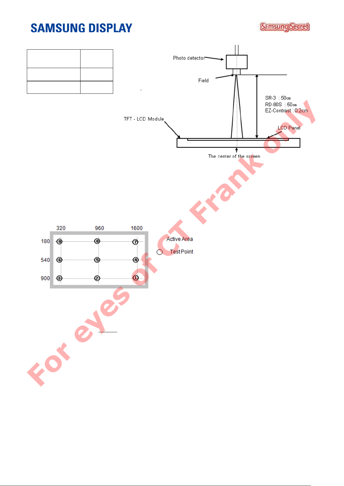
- Definition of the test point
Note (1) Definition of contrast ratio (C/R)
: The ratio of gray max (Gmax) & gray min (Gmin) at the center point ⑤ of the panel
The measurement goes in ELABO-LS Standard light source
Gmax : The luminance with all white pixels
Gmin : The luminance with all black pixels
——————————————————————————————————————————————––—
Doc.No. LSC400HM06-T Page 7 of 37 Rev.No. 06-000-G-20130404
Page 8
————————————————————————————————————————————————–
Display data
The response of
optical instruments
For eyes of CT Frank only
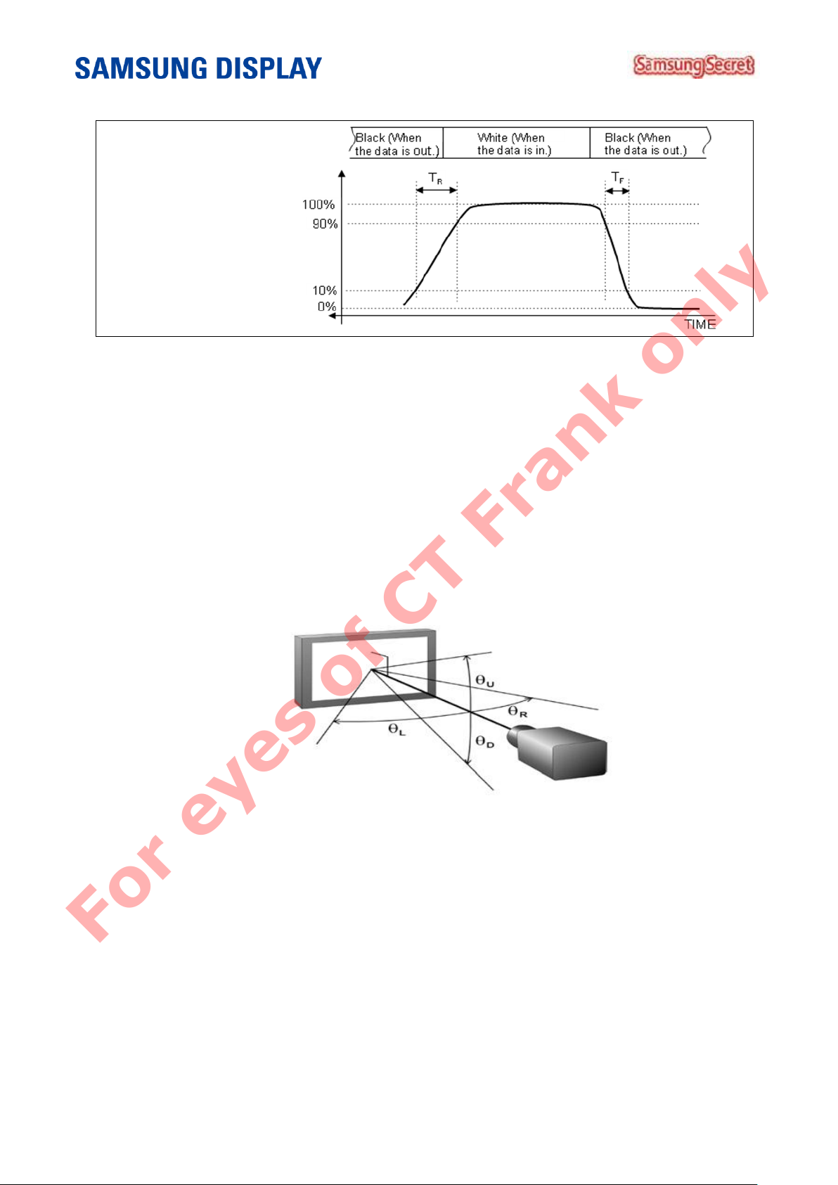
Note (2) Definition of response time
※ G-to-G : Average response time between the whole gray scale to the whole gray scale.
The response time is the value that was measured after it was operated in Samsung's standard BLU for one
hour.( at room temperature)
Note (3) Definition of transmissivity.
The measurement shall be executed with the standard light source of D65.
Note (4) The definition of chromaticity (CIE 1931)
The color coordinate of red, green, blue and white at the center point ⑤
The measurement shall be executed with the standard light source of D65
Note (5) Definition of viewing angle
: The range of viewing angle (C/R ≥10)
The measurement shall be executed with the standard light source of D65
——————————————————————————————————————————————––—
Doc.No. LSC400HM06-T Page 8 of 37 Rev.No. 06-000-G-20130404
Page 9
————————————————————————————————————————————————–
Item
Symbol
Min.
Typ.
Max.
Unit
Note
Voltage of power supply
VDD
10.8
12.0
13.2 V (1)
Currnet of
power
supply
(a) Black
IDD
-
500
600
mA
(2),(3)
(b) White
-
470
550
mA
(c) Sub H-Stripe
-
800
1000
mA
Vsync frequency
fV
48
60
62.5
Hz Hsync frequency
fH
60
67.5
70
kHz Main frequency
Fdclk
130
148.5
152.5
MHz Rush current
IRUSH
-
-
3
A
(4)
For eyes of CT Frank only
4. ELECTRICAL CHARACTERISTICS
4.1 TFT LCD MODULE
* Ta = 25 ± 2 °C
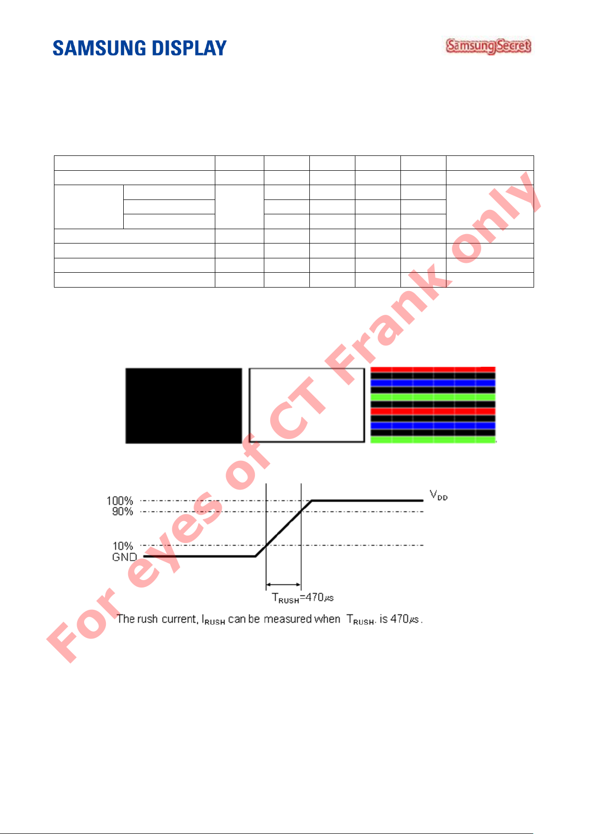
Note (1) The ripple voltage should be controlled fewer than 10% of V
(2) fV=60Hz, fDCLK = 148.5MHz, VDD = 12.0V, DC Current.
(3) Power dissipation check pattern (LCD Module only)
(a) Black (b) White (c) Sub H-Stripe
(Typ.) voltage.
DD
(4) Conditions for measurement
——————————————————————————————————————————————––—
Doc.No. LSC400HM06-T Page 9 of 37 Rev.No. 06-000-G-20130404
Page 10
————————————————————————————————————————————————–
Pin
Symbol
Description
Pin
Symbol
Description
1
NC
NOTE1
26
NC
NOTE1
2
NC
NOTE1
27
NC
NOTE1
3
NC
NOTE1
28
Rx2[A]N
Even LVDS Signal -
4
NC
NOTE1
29
Rx2[A]P
Even LVDS Signal +
5
NC
NOTE1
30
Rx2[B]N
Even LVDS Signal -
6
NC
NOTE1
31
Rx2[B]P
Even LVDS Signal +
7
LVDS selection
NOTE2
32
Rx2[C]N
Even LVDS Signal -
8
NC
NOTE1
33
Rx2[C]P
Even LVDS Signal +
9
NC
NOTE1
34
GND
Ground
10
NC
NOTE1
35
Rx2CLK-
LVDS Clock -
11
GND
Ground
36
Rx2CLK+
LVDS Clock +
12
Rx1[A]N
Odd LVDS Signal -
37
GND
Ground
13
Rx1[A]P
Odd LVDS Signal +
38
Rx2[D]N
Even LVDS Signal -
14
Rx1[B]N
Odd LVDS Signal -
39
Rx2[D]P
Even LVDS Signal +
15
Rx1[B]P
Odd LVDS Signal +
40
Rx2[E]N (Note 2)
Even LVDS Signal -
16
Rx1[C]N
Odd LVDS Signal -
41
Rx2[E]P (Note 2)
Even LVDS Signal +
17
Rx1[C]P
Odd LVDS Signal +
42
NC
NOTE1
18
GND
Ground
43
NC
NOTE1
19
Rx1CLK-
LVDS Clock -
44
GND
Ground
20
Rx1CLK+
LVDS Clock +
45
GND
Ground
21
GND
Ground
46
GND
Ground
22
Rx1[D]N
Odd LVDS Signal -
47
NC
NOTE1
23
Rx1[D]P
Odd LVDS Signal +
48
12V
DC power supply
24
Rx1[E]N (Note 2)
Odd LVDS Signal -
49
12V
DC power supply
25
Rx1[E]P (Note 2)
Odd LVDS Signal +
50
12V
DC power supply
51
12V
DC power supply
For eyes of CT Frank only
5. INPUT TERMINAL PIN ASSIGNMENT
5.1 INPUT SIGNAL & POWER
Connector : FI-RXE51S-HF (JAE)
——————————————————————————————————————————————––—
Doc.No. LSC400HM06-T Page 10 of 37 Rev.No. 06-000-G-20130404
Page 11
————————————————————————————————————————————————–
NOTE(2) Parameter
Symbol
Value
Unit
Note
Min
Typ
Max
Interface
Input High Voltage
High
2.8 - 3.6
V
Input Low Voltage
Low 0 -
0.8
V
For eyes of CT Frank only
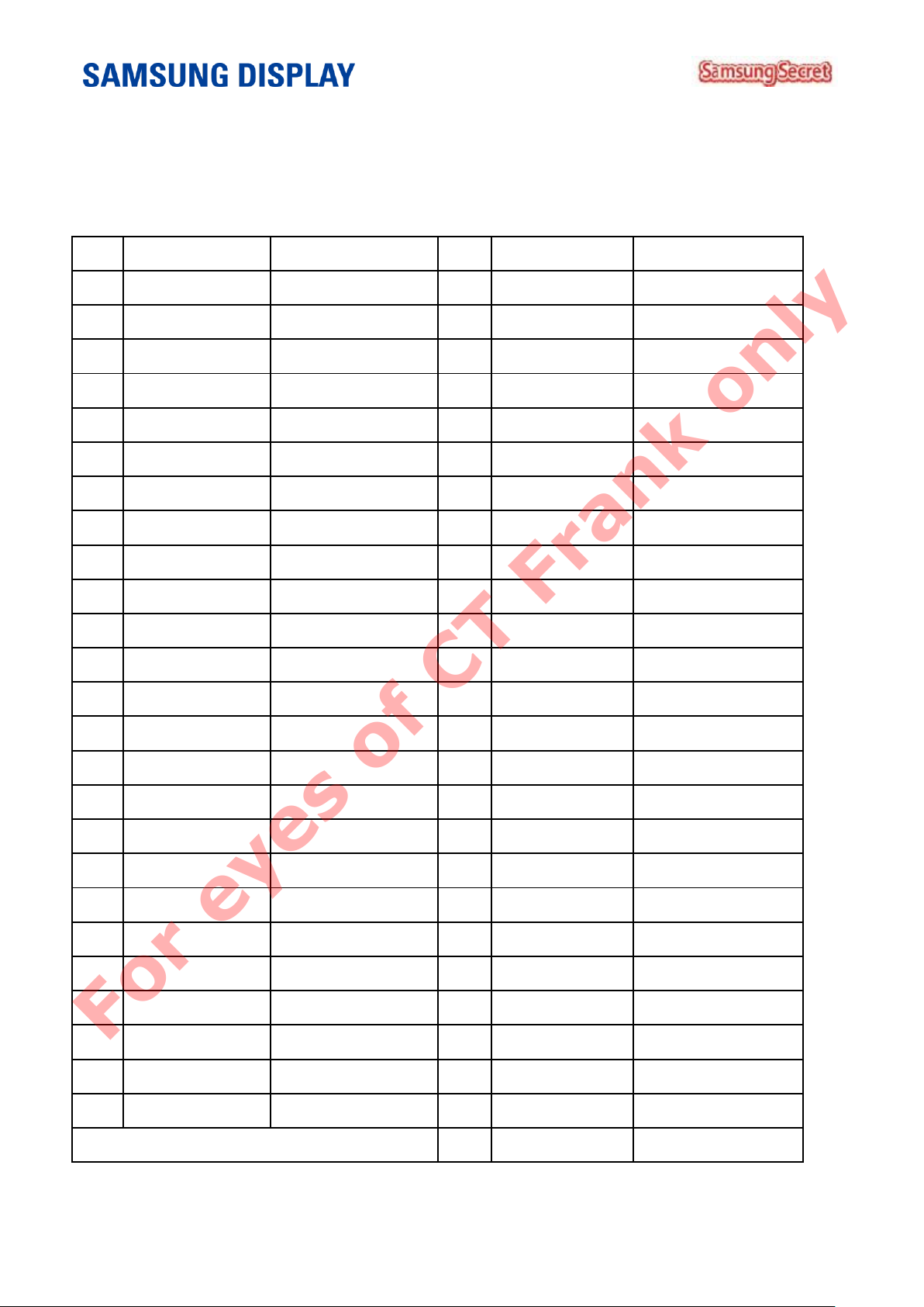
Note (1) No connection: These PINS are used only for the product of SAMSUNG.
(DO NOT CONNECT the input device to these pins.)
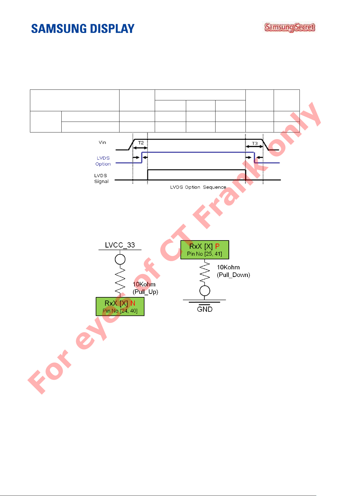
Note (2) LVDS selection : If this pin : Low(GND V) / NC JEIDA LVDS format
Otherwise : High(3.3V) Normal LVDS
Note (3) Input mode 8bit setting @ 8bit input E_Channel : Floating
Input mode 10bit setting @ 8bit input E_Channel : Keep Level’0’
Pin No.24 / Pin No.40 : Pull up(3.3V)
Pin No.25 / Pin No.41 : Pull down(GND)
——————————————————————————————————————————————––—
Doc.No. LSC400HM06-T Page 11 of 37 Rev.No. 06-000-G-20130404
Page 12
————————————————————————————————————————————————–
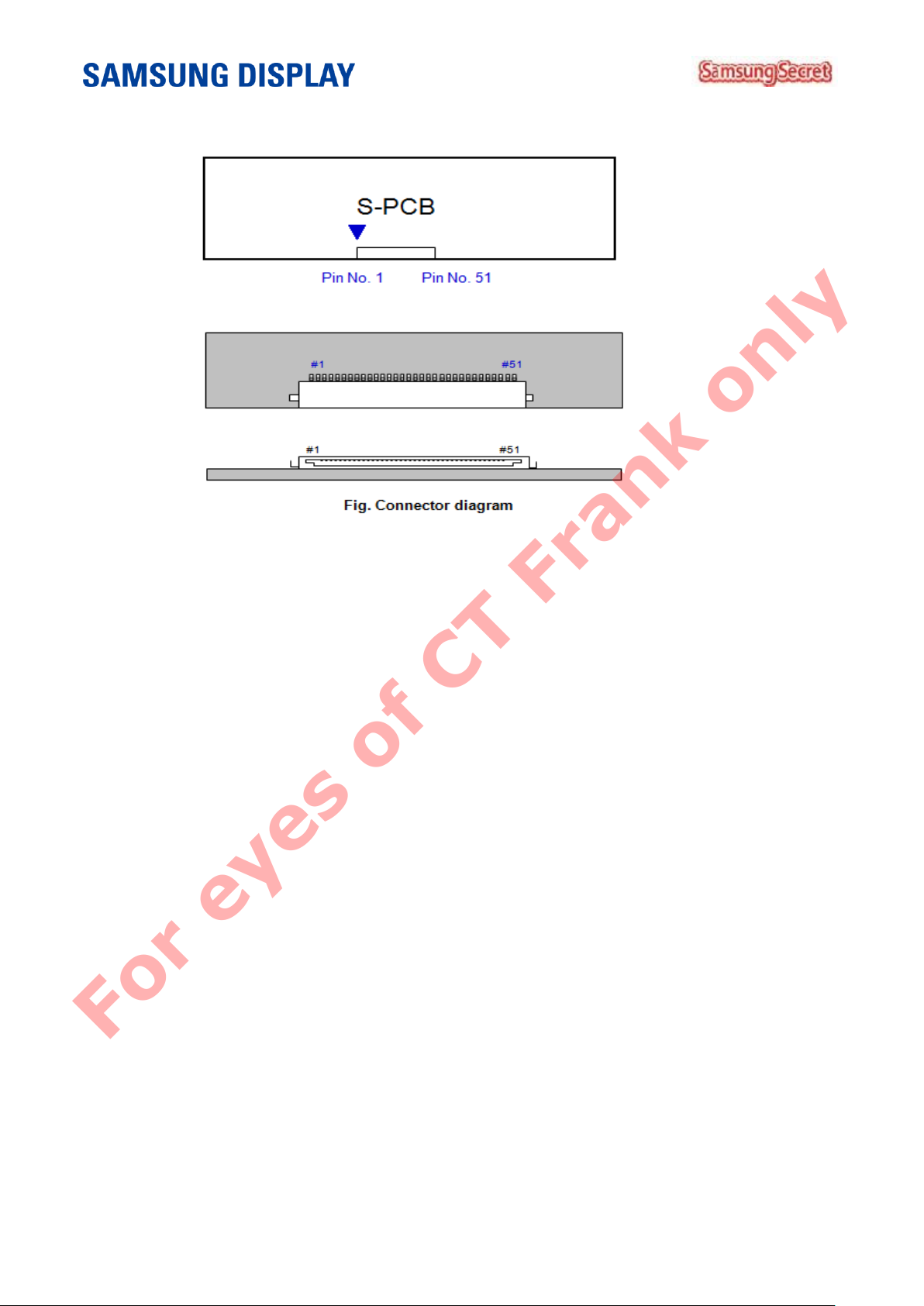
Fig . The diagram of connector
For eyes of CT Frank only
Note (4) Pin number which starts from the left side.
a. Power GND pins should be connected to the LCD’s metal chassis.
b. All power input pins should be connected together.
c. All NC pins should be separated from other signal or power.
——————————————————————————————————————————————––—
Doc.No. LSC400HM06-T Page 12 of 37 Rev.No. 06-000-G-20130404
Page 13
————————————————————————————————————————————————–
LVDS pin
VESA (Normal)
JEIDA
TxOUT/RxINA
TxIN/RxOUT0
R0
R4
TxIN/RxOUT1
R1
R5
TxIN/RxOUT2
R2
R6
TxIN/RxOUT3
R3
R7
TxIN/RxOUT4
R4
R8
TxIN/RxOUT6
R5
R9
TxIN/RxOUT7
G0
G4
TxOUT/RxINB
TxIN/RxOUT8
G1
G5
TxIN/RxOUT9
G2
G6
TxIN/RxOUT12
G3
G7
TxIN/RxOUT13
G4
G8
TxIN/RxOUT14
G5
G9
TxIN/RxOUT15
B0
B4
TxIN/RxOUT18
B1
B5
TxOUT/RxINC
TxIN/RxOUT19
B2
B6
TxIN/RxOUT20
B3
B7
TxIN/RxOUT21
B4
B8
TxIN/RxOUT22
B5
B9
TxIN/RxOUT24
HSYNC
HSYNC
TxIN/RxOUT25
VSYNC
VSYNC
TxIN/RxOUT26
DEN
DEN
TxOUT/RxIND
TxIN/RxOUT27
R6
R2
TxIN/RxOUT5
R7
R3
TxIN/RxOUT10
G6
G2
TxIN/RxOUT11
G7
G3
TxIN/RxOUT16
B6
B2
TxIN/RxOUT17
B7
B3
TxIN/RxOUT23
RESERVED
RESERVED
TxOUT/RxINE
TxIN/RxOUT28
R8
R0
TxIN/RxOUT29
R9
R1
TxIN/RxOUT30
G8
G0
TxIN/RxOUT31
G9
G1
TxIN/RxOUT32
B8
B0
TxIN/RxOUT33
B9
B1
TxIN/RxOUT34
RESERVED
RESERVED
For eyes of CT Frank only
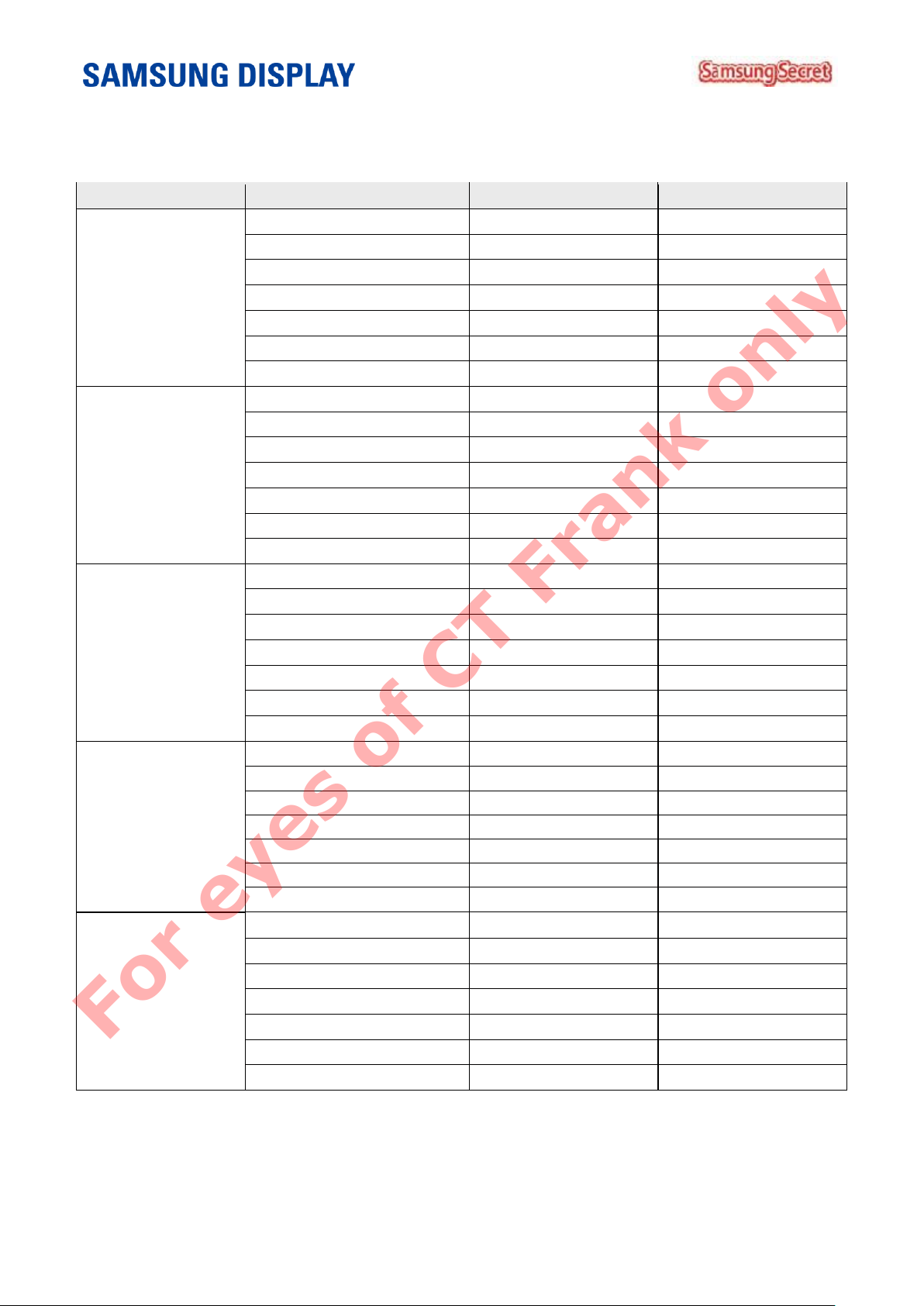
5.2 LVDS INTERFACE
- LVDS receiver : T-con(merged)
- Data format
——————————————————————————————————————————————––—
Doc.No. LSC400HM06-T Page 13 of 37 Rev.No. 06-000-G-20130404
Page 14
————————————————————————————————————————————————–
For eyes of CT Frank only
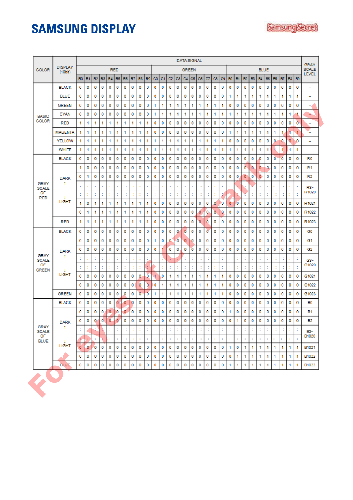
5.3 INPUT COLOR DATA MAPPING
Note (1) Definition of gray : Rn: Red gray, Gn: Green gray, Bn: Blue gray (n=gray level)
Note (2) Input signal: 0 =Low level voltage, 1=High level voltage
——————————————————————————————————————————————––—
Doc.No. LSC400HM06-T Page 14 of 37 Rev.No. 06-000-G-20130404
Page 15
————————————————————————————————————————————————–
Signal
Item
Symbol
Min.
Typ.
Max.
Unit
Note
Clock
Frequency
1/TC
130
148.5
160
MHz - Hsync
FH
60
67.5
70
KHz - Vsync
FV
48
60
62.5
Hz
-
Term for the
Vertical
Display
Active display
period
TVD
1080
Lines
-
Total vertical
TV
1110
1125
1400
Lines
-
Term for the
Horizontal
Display
Active display
Period
THD
1920
Clocks
-
Total
Horizontal
TH
2092
2200
2348
clocks
-
For eyes of CT Frank only
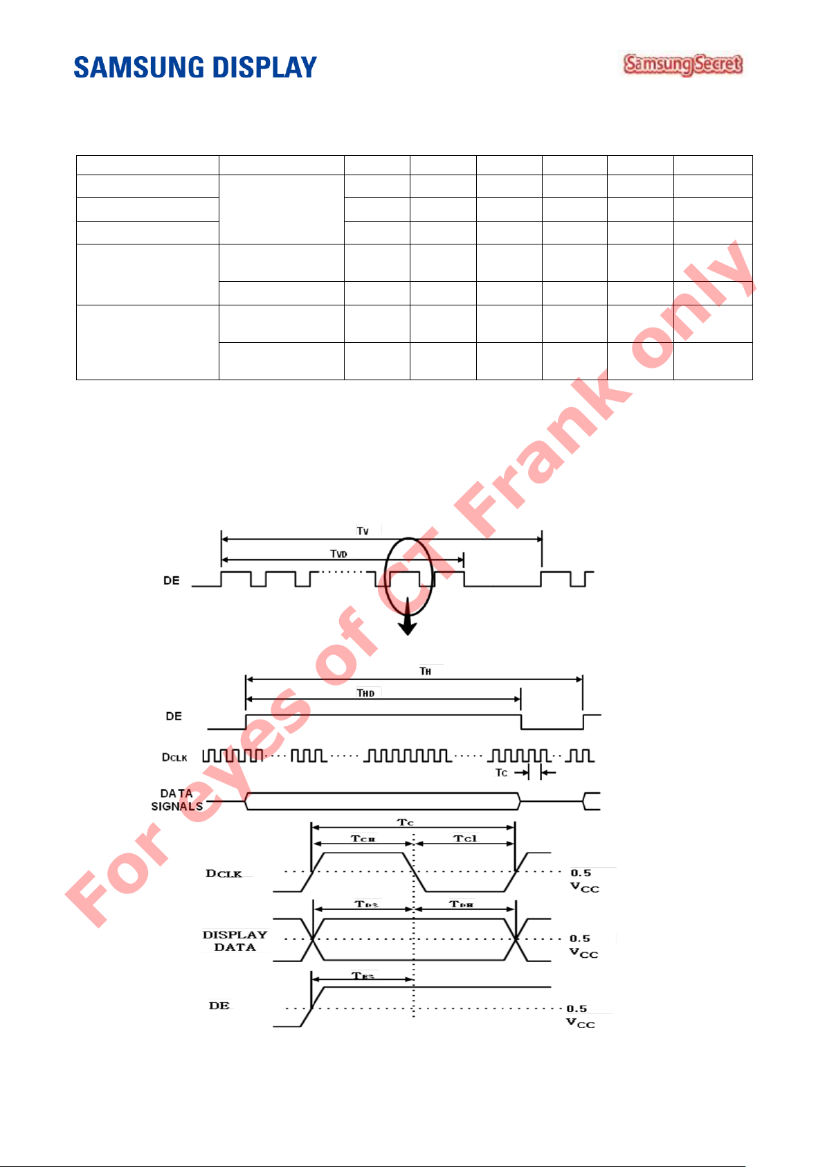
6. INTERFACE TIMING
6.1 TIMING PARAMETERS OF TIMING (Only DE Mode)
Note) These products don’t have to receive the signal of Hsync & Vsync from the input device.
(1)Key points when testing: TTL controls the signal and the CLK at the input terminal of LVDS Tx of the system.
(2) Internal VDD = 3.3V
(3) Spread spectrum
* The limit of spread spectrum's range of SET in which the LCD module is assembled should be within ± 1.5%.
6.2 TIMING DIAGRAMS OF INTERFACE SIGNAL
——————————————————————————————————————————————––—
Doc.No. LSC400HM06-T Page 15 of 37 Rev.No. 06-000-G-20130404
Page 16
————————————————————————————————————————————————–
ITEM
SYMBOL
Min.
Typ.
Max.
UNIT
NOTE
Differential input high
threshold voltage
VTH
- - 100
mV
VCM=1.2V
Differential input low
threshold voltage
VTL
-100 - -
mV
Input common mode voltage
VCM
0.2 - 2.0 V Differential Input Voltage
|VID|
100 - 600
mV
Input data position
FIN=80MHz
t
RSRM
- - 450
ps
t
RSLM
-450 - -
ps
For eyes of CT Frank only
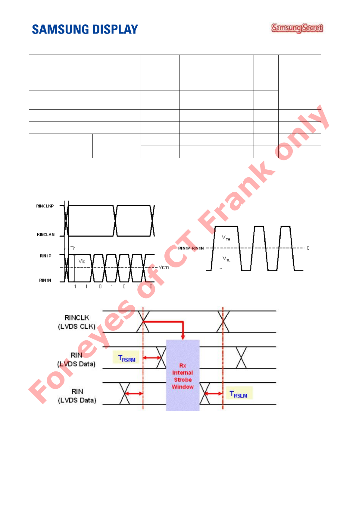
6.3 CHARACTREISTICS OF INPUT DATA OF LVDS
Notice The spread spectrum should be 0% when the skew is measured.
Position of a measurement is T-CON LVDS input pin
——————————————————————————————————————————————––—
Doc.No. LSC400HM06-T Page 16 of 37 Rev.No. 06-000-G-20130404
Page 17
————————————————————————————————————————————————–
For eyes of CT Frank only
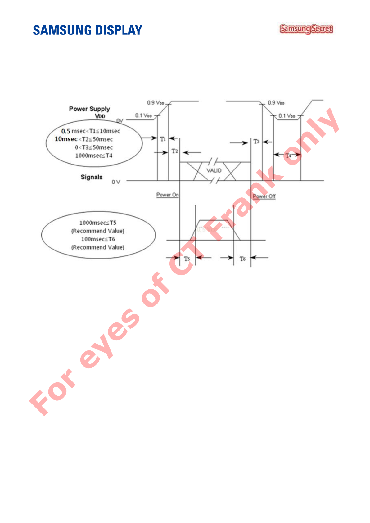
6.4 POWER ON/OFF SEQUENCE
To prevent the product from being latched up or the DC in the LCD module from starting an operation, the
order to turn the power on and off should be changed to the order as shown in the diagram below.
T1 : The VDD rising time from 10% to 90%
T2 : The time from the point which V
the power is on.
T3: The time from the point which the valid data is out to the point which VDD reach to the 90% of voltage
when the power is off.
T4: the time from the point which the Vdd decrease to the point which the Vdd increase again for windows to
restart.
※ The recommended operating condition of the back light system
T5: The time which takes for B/L to be turned on after the signal is entered when the time is on.
T6 : The time which takes until the signal is out after BL is turned off
The condition of supply voltage to enter in the module from the external system should have the
same condition as the definition of VDD.
Apply the voltage for the lamp within the range which the LCD operates. when the back light is turned on
before the LCD is operated or when the LCD is turned off before the back light is turned off, the display
may show the abnormal screen momentarily.
While the V
The figure of T4 should be measured after the module has been fully discharged between the periods
when the power is on and off.
The interface signal must not keep the high impedance condition when the power is on.
is off level, please keep the level of input signals low or keep a high impedance condition.
DD
reach to 90% of voltage to the point which the valid data is out when
DD
——————————————————————————————————————————————––—
Doc.No. LSC400HM06-T Page 17 of 37 Rev.No. 06-000-G-20130404
Page 18
ACTIVE CENTER
For eyes of CT Frank only
Page 19
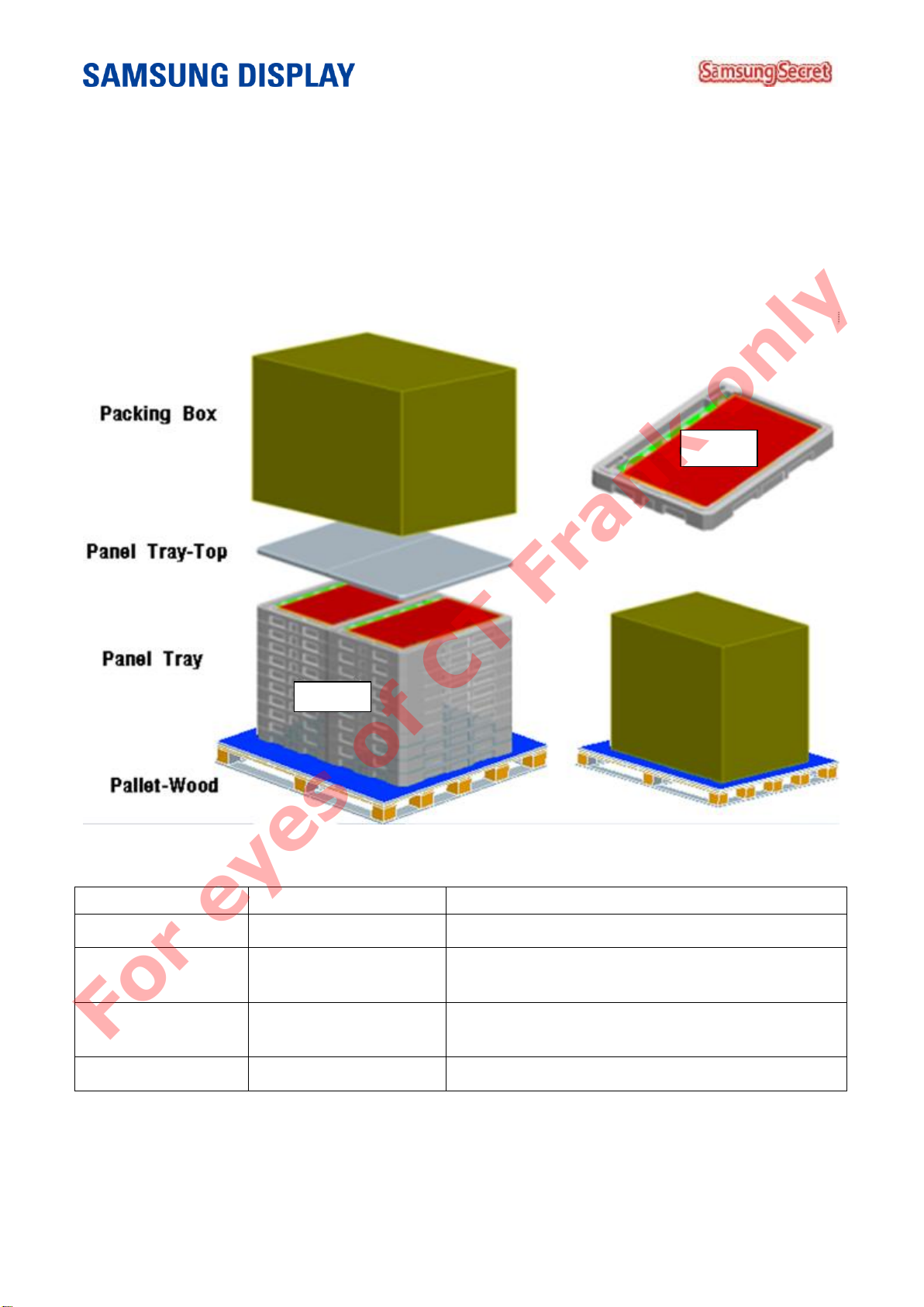
————————————————————————————————————————————————–
ITEM
Specification
Remark
Total Pallet Size
1485 X 1150 X 1192
W x V x Height [mm]
Tray
7 [Panel/Tray]
-. Panel : 13.3kg(1.9kg/Panel, 7ea/Tray)
-. Panel Tray : 1.6kg(EPS)
Pallet
20 [Tray/Pallet]
-. Pallet 28.0kg(Wood Pallet)
-. 20ea(10tray x 2array) + 2ea(Top tray)
Total Weight
339.0 [kg]
-. Packing Box : 3kg(Paper)
7EA
20EA
For eyes of CT Frank only
8. PACKING
8.1 CARTON
(1) Packing Form
Corrugated Card board box as shock absorber.
(2) Packing Method
(3) Packing Material
——————————————————————————————————————————————––—
Doc.No. LSC400HM06-T Page 19 of 37 Rev.No. 06-000-G-20130404
Page 20
————————————————————————————————————————————————–
Panel number
Cell ID
Lot ID
Month
Year
Product Code
For eyes of CT Frank only
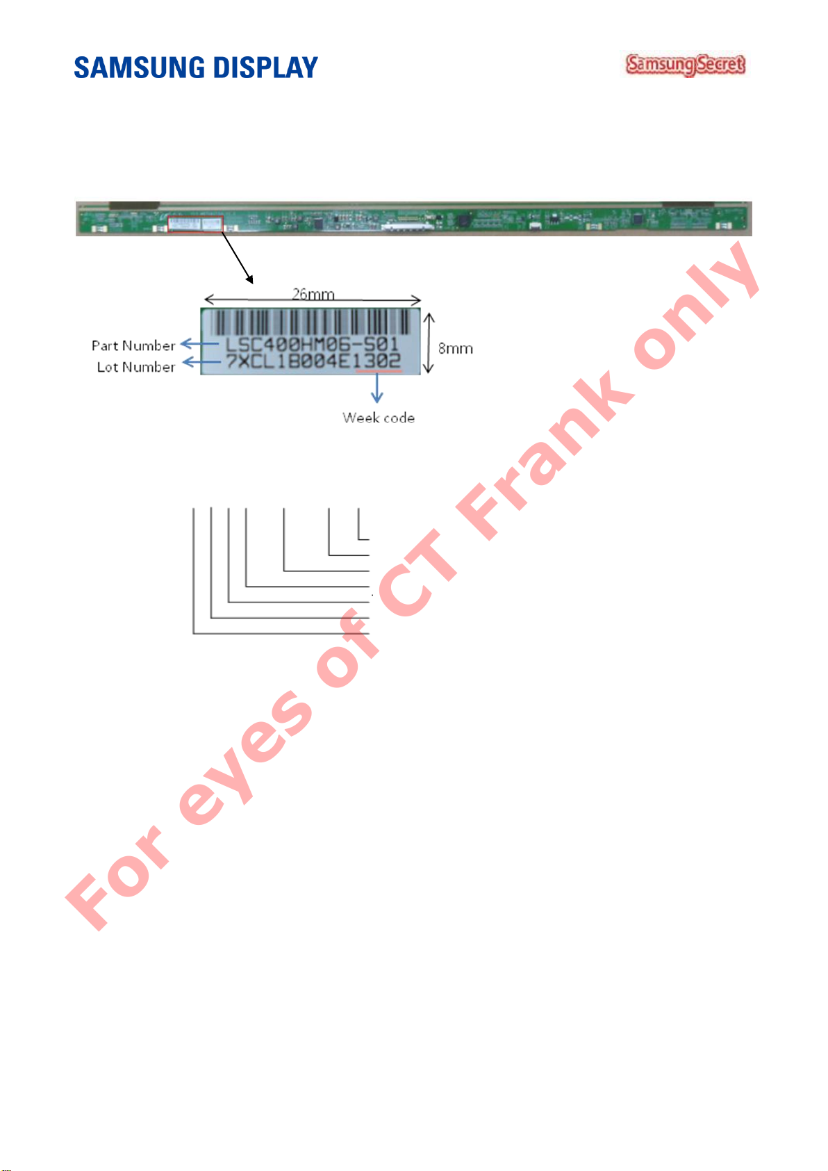
8.2 MARKING
A nameplate is affixed to the specified location on each product.
(1)Parts number : LSC400HM06
(2)Revision code : 3 letters
(3)Lot number : X X X X XXX XX X
(4) Weekcode : 1205( ex. 2012 year, 5th week)
——————————————————————————————————————————————––—
Doc.No. LSC400HM06-T Page 20 of 37 Rev.No. 06-000-G-20130404
Page 21
————————————————————————————————————————————————–
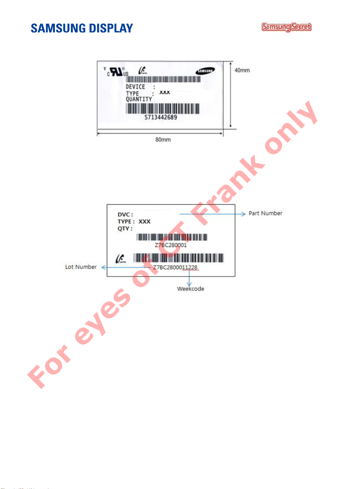
LSC400HM06-xxx
For eyes of CT Frank only
(4) Nameplate Indication
Parts name : LSC400HM06
Lot number : XXXXXXXXXX
Product Revision Code : XXX
(5) Packing box attach
——————————————————————————————————————————————––—
Doc.No. LSC400HM06-T Page 21 of 37 Rev.No. 06-000-G-20130404
Page 22

————————————————————————————————————————————————–
No.
Item
Control standard
1
Ionizer
All Equipment should be controlled under 150V.(Typ. 100V)
2
Carrying Roller
Carrying Roller should be controlled under 200V.
3
Equipment Ground Resistance
All Equipment Ground Should be less than 1ohm.
For eyes of CT Frank only
9. GENERAL PRECAUTIONS
9.1 HANDLING
(a) When the panel kit and BLU kit are assembled, the panel kit and BLU kit should be attached to the set
system firmly by combining each mounted holes. Be careful not to give the mechanical stress.
(b) Be careful not to give any extra mechanical stress to the panel when designing the set, and BLU kit.
(c) Be cautious not to give any strong mechanical shock and / or any forces to the panel kit.
Applying the any forces to the panel may cause the abnormal operation or the damage to the panel kit and
the back light unit kit.
(d) Refrain from applying any forces to the source PBA and the drive IC in the process of the handling or
installing to the set. If any forces are applied to the products, it may cause damage or a malfunction in the
panel kit.
(e) Refrain from applying any forces which cause a constant shock to the back side of panel kit, the set
Design and BLU kit. If any forces are applied to the products, it may cause an abnormal display, a functional
failure and etc.
(f) Note that polarizer could be damaged easily.
Do not press or scratch the bare surface with the material which is harder than a HB pencil lead.
(g) Wipe off water droplets or oil immediately. If you leave the droplets for a long time on the product, a
staining or the discoloration may occur.
(h) If the surface of the polarizer is dirty, clean it using the absorbent cotton or the soft cloth.
(i) Desirable cleaners are water or IPA (Isopropyl Alcohol).
Do not use Kenton type materials (ex. Acetone), Ethyl alcohol, Toluene, Ethyl acid or Methyl chloride. These
might cause the permanent damage to the polarizer due to chemical reaction.
(j) If the liquid crystal material leaks from the panel, this should be kept away from the eyes or mouth.
If this contacts to hands, legs, or clothes, you must washed it away with soap thoroughly and see a doctor
for the medical examination.
(k) Protect the panel kit and BLU Kit out of the static electricity. Otherwise the circuit IC could be damaged.
- Reference : Process control standard of SDC
——————————————————————————————————————————————––—
Doc.No. LSC400HM06-T Page 22 of 37 Rev.No. 06-000-G-20130404
Page 23
————————————————————————————————————————————————–
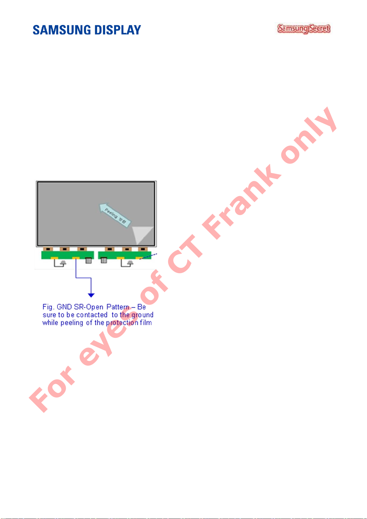
- Make sure to peel off slowly
(It is recommended to peel it off at the speed of more than
8sec. constantly.)
- The peeling direction is shown at the Fig
- Instruct the ground worker to work with the adequate
methods such as the antistatic wrist band.
- Maker sure to be grounded the source PBA while peeling of
the protection film.
- Ionized air should be blown over during the peeling
- The protection film should not t be contacted to the source
drive IC.
- If the adhesive stains remain on the polarizer after the
protection film is peeled off, please move stains with
isopropyl-alcohol liquid.
For eyes of CT Frank only
(l) Remove the stains with finger-stalls wearing soft gloves in order to keep the display clean in the process of
the incoming inspection and the assembly process.
(m) Do not pull or fold the source drive IC which connects to the source PBA and the panel or the gate drive
IC.
(n) Do not pull, fold or bend the source drive IC and the gate drive IC in any processes.
If not, the source drive IC could be bent one time in the process of assembling the panel Kit and the BLU
Kit.
(o) Do not adjust the variable resistor located on the panel kit and BLU kit except when adjusting the flicker.
(p) Do not touch the pins of the interface connector directly with bare hands.
(q) Be cautious not to be peeled off the protection film.
(r) The protection film for the polarizer on the panel kit should be slowly peeled off just before using so that
the electrostatic charge can be minimized.
(s) The panel kit and BLU kit have high frequency circuits. The sufficient suppression to the EMI should be
done by the set manufacturers.
(t) The set of which the panel is assembled shall not be twisted. If the product is twisted, it may cause the
damage on the product.
(u) Surface Temp. of IC should be controlled less than 100℃, operating over the Temp. can cause the damage
or decrease of lifetime.
——————————————————————————————————————————————––—
Doc.No. LSC400HM06-T Page 23 of 37 Rev.No. 06-000-G-20130404
Page 24
————————————————————————————————————————————————–
ITEM
Unit
Min.
Max.
Storage
Temperature
(℃)
5
40
Storage
Humidity
(%rH)
35
75
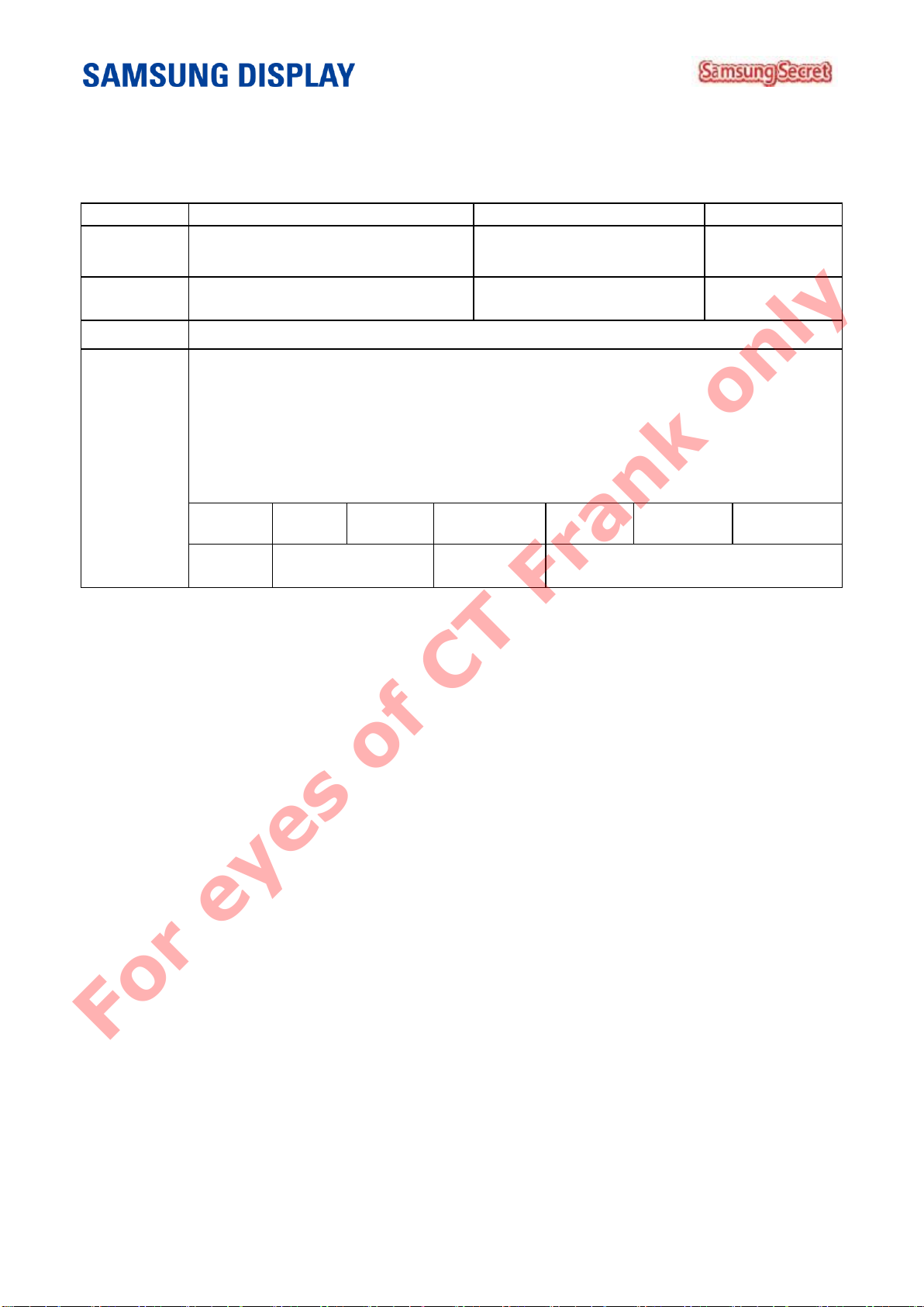
Storage life
6 months
Storage
Condition
(1) The storage room should provide good ventilation and temperature control.
(2) Products should not be placed on the floor, but on the Pallet away from a wall.
(3) Prevent products from direct sunlight, moisture nor water; Be cautious of a buildup of
condensation.
(4) Avoid other hazardous environment while storing goods.
(5) If products delivered or kept in conditions of the recommended temperature or humidity,
we recommend you leave them at a circumstance which is shown in the following table.
period
1 month
2 months
3 months
4 months
5 months
6 months
Baking
Condition
No Baking
50℃, 10%
24Hr
50℃, 10%, 48Hr
For eyes of CT Frank only
9.2 STORAGE
The storage condition for packing
9.3 OPERATION
(a) Do not connect or disconnect the FFC cable during the "Power On" condition.
(b) Power supply should be always turned on and off by the "Power on/off sequence"
(c) The module has high frequency circuits. The sufficient suppression to the electromagnetic interference
should be done by the system manufacturers. The grounding and shielding methods is important to minimize
the interference.
(d) The cables between TV SET connector and Control PBA interface cable should be connected directly to
have a minimized length. A longer cable between TV SET connector and Control PBA interface cable maybe
operate abnormal display
(e) Recommend to age for over 1 hour at least in the state, which the product is driving initially to stabilize the
characteristic of the initial TFT.
(f) Response time depends on the temperature.( In Lower temperature, it becomes longer)
——————————————————————————————————————————————––—
Doc.No. LSC400HM06-T Page 24 of 37 Rev.No. 06-000-G-20130404
Page 25
————————————————————————————————————————————————–
Pin. No.
Symbol
Function
Remark
1
TCON_WP
EN
Default : 0V
Vcom tunning : 3.3V
(Shouldn’t be communicated with I2C device as output level
“5V”)
2
SCL_I
I2C Interface
I2C Bus Interface
3
SDA_I
I2C Interface
Type
Flicker data saving position
Slave Address
Genie Type
Gamma IC memory
Write B0 = “0”/Read B0 =”1”
Genie-lite Type
T-con EEPROM
1110101 (EEPROM data Address : 8161)
For eyes of CT Frank only
9.4 OPERATION CONDITION GUIDE
(a) The LCD product shall be operated under normal conditions.
The normal condition is defined as below;
- Temperature : 20± 15℃
- Humidity : 55± 20%
- Display pattern : continually changing pattern (Not stationary)
(b) If the product will be used under extreme conditions such as under the high temperature, humidity,
display patterns or the operation time etc.., it is strongly recommended to contact SDC for the advice about
the application of engineering . Otherwise, its reliability and the function may not be guaranteed. Extreme
conditions are commonly found at airports, transit stations, banks, stock markets, and controlling systems.
9.5 PROCESS EXECUTING GUIDE
(a) Aging
Be sure to age for over 1 hour at least, which the product is driving initially to stabilize TFT Characteristic.
(b) Flicker Adjustment
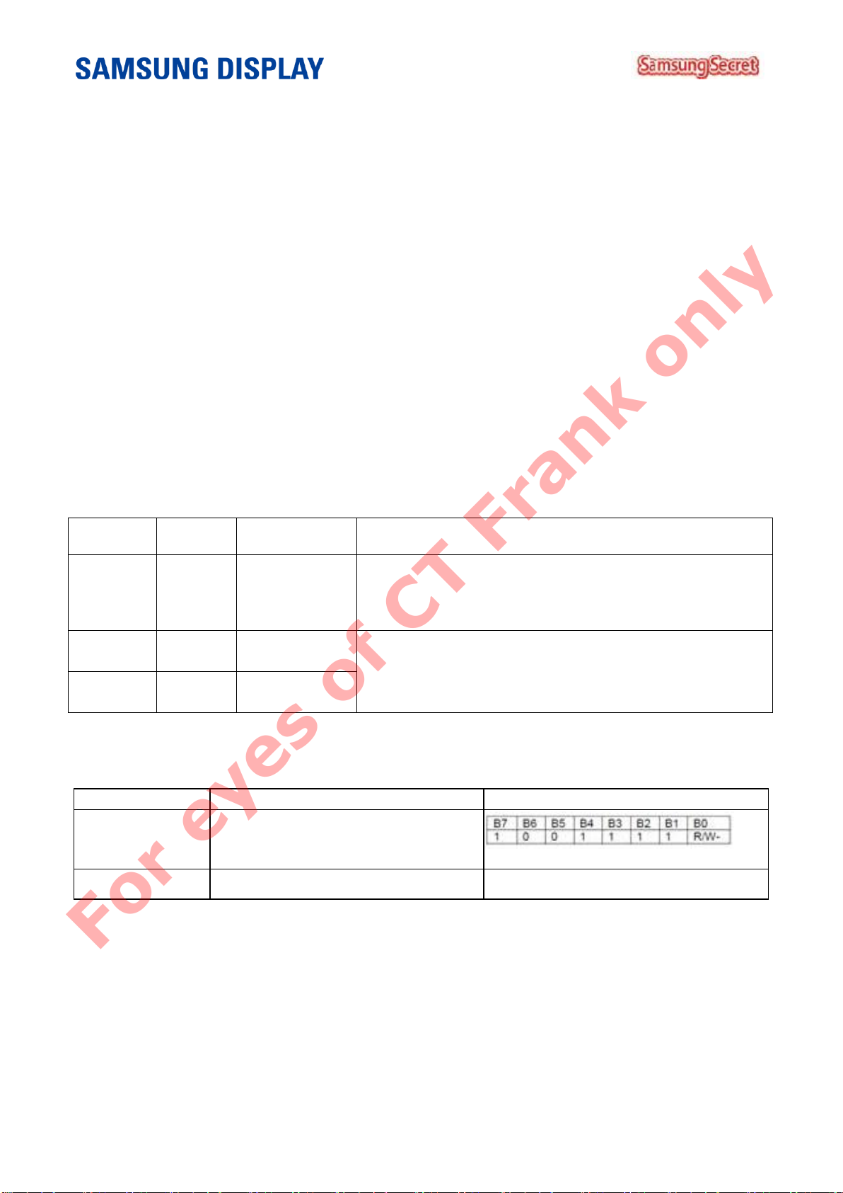
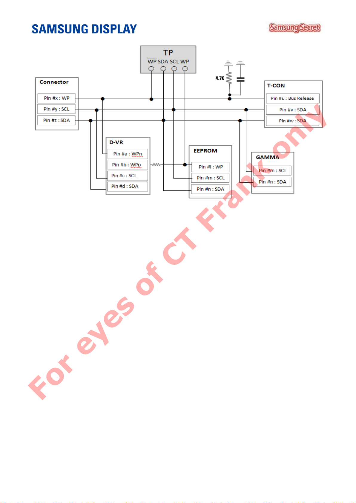
(1) Flicker should be adjusted by optimizing the Vcom value in customer LCM Line through the I2C Interface.
(Master & Slave = I2C communication )
(2) Flicker should be tuned by correct method according to gamma IC type of each model and
(LSC400HM06 – “Genie Type”)
(3) Flicker should be adjusted the pattern, where are displayed alternately at green sub-pixel. (Green 1*1 Dot
Pattern)
——————————————————————————————————————————————––—
Doc.No. LSC400HM06-T Page 25 of 37 Rev.No. 06-000-G-20130404
Page 26
————————————————————————————————————————————————–
For eyes of CT Frank only
< Flicker Adjust Circuit Block Diagram >
9.6 OTHERS
(a) The ultra-violet ray filter is necessary for the outdoor operation.
(b) Avoid the condensation of water which may result in the improper operation of product or the
disconnection of
electrode.
(c) Do not exceed the limit on the absolute maximum rating. (For example, the supply voltage variation, the
input voltage variation, the variation in content of parts and environmental temperature, and so on) If not,
panel may be damaged.
(d) If the module keeps displaying the same pattern for a long period of time, the image may be remained to
the screen. To avoid the image sticking, it is recommended to use a screen saver.
(e) This Panel has its circuitry of PCB's on the rear side, so it should be handled carefully in order for a force
not to be applied.
(f) Please contact the SDC in advance when the same pattern is displayed for a long time
——————————————————————————————————————————————––—
Doc.No. LSC400HM06-T Page 26 of 37 Rev.No. 06-000-G-20130404
Page 27
————————————————————————————————————————————————–
No
.
Component
Expected cause
1
Upholding part for
panel
Prevent the panel from breaking by assigning gaps between the panel and the upholding part for panel on the drawing
for the upholding part for panel.
Refer to the (a), (b), (c) of 3-1 for the design of BLU.
2
The shape of the
upholding part for
panel
Design the upholding part for panel to fit to the panel appropriately when designing the BLU since the shape of the
upholding part for panel may damage the panel.
Refer to the (a), (b), (c) of 3-1 for the design of BLU.
3
The edge of
upholding part for
panel
Design the edge of panel to have a sufficient space with the upholding part for panel when designing the BLU since the
edge of the upholding part for panel may damage the panel when assembling the panel and BLU.
Refer to the (a), (b), (c) of 3-1 for the design of BLU.
4
Upholding part for
panel
Place the upholding part for the panel in order for the shape of mold, which contacts with the panel not to interfere
with the area of panel.
Refer to the (a), (b), (c) of 3-1 for the design of BLU.
5
Drive IC
Design the BLU in order for the COF not to contain the lead crack resulted from the tensioned COF created when the
product is twisted if the space between the D-IC COF and the middle mold isn't sufficient.
Refer to the (a), (b), (c),(d),(e),(f), and (g)of 3-2 for the design of BLU.
6
Drive IC
Design the BLU in order for the product not to contain the lead crack resulted from the tensioned COF caused under the
condition, which the product is twisted by fixing the source PCB.
Refer to the (a), (b), (c),(d),(e),(f), and (g)of 3-2 for the design of BLU.
7
IC
component
1) The temperature of each part of product suggested by our company and the second vendor shall meet the standard
of temperature, which is recommended not to be exceeded by our company when the product is affected under the
various temperature ranges.
Apply over 1mm long separation distance stated in the safety standard between the electric part and each conductor.
(Apply the rated separation distance when insulating.)
8
Thermal pad
Apply the thermal pad in a designated size to the product as a measure to lower the temperature of heat in order for
each part to use the rated temperature.
9
POL
The surrounding area of the POL shall be treated with an electrification treatment since the external ESD may cause a
phenomenon, which the POL is coming off.
In addition, the GND portion of source PBA shall be grounded.
10
PBA
The GND portion of each PBA shall be contacted with the GND portion of BLU.
Refer to the (a) and (b) of 3-3 for the design of BLU.
11
Circuit
The standardized approval from the client is required since the EMI is executed by a client.
Our company can only measure the reference since the client measures the BLU.
12
The height of
component
Design the BLU with considering the maximum height of parts, which our company suggests.
13
Between the FFC and
the C-PBA
Design the instrument with considering the length between the FFC and the control PBA.
(The marginal minimum length of 5mm or 8mm is required.)
14
Panel
The surface temperature of panel shall be maintained within 0℃ and 45℃ when the external ambient temperature is at
25℃. (Design the BLU with considering the increase of the temperature in the panel by the LED, CCFL, and etc.)
15
Aging
Recommend to age for over 1 hour at least in the state, which the product is driving initially to stabilize the
characteristic of the initial TFT.
16
The attachment of
gasket
The additional confirmation by our company is required If the attachment of gasket to the S-PBA of our company is
required.(To fix the S-PBA or the EMI)
17
Drive IC
Design the top chassis and the driver IC to be contacted by placing the shape of emboss inside the top chassis as a
measure to prevent the driver IC from heating. The size of emboss shall be designed in larger size than the size of IC
inside the film of the driver IC.
Refer to the (a), (b), (c),(d),(e),(f), and (g)of 3-2 for the design of BLU.
18
The prohibited
bandwidth
Design the BLU in order for the BLU not to interfere with the area, where the control PBA and the source PBA are
located densely according to the drawing for the BLU from our company.
19
S-PBA
The material, which contacts with the bottom side of S-PBA which has a pattern shall be non-conducting material or
shall be insulated.
For eyes of CT Frank only
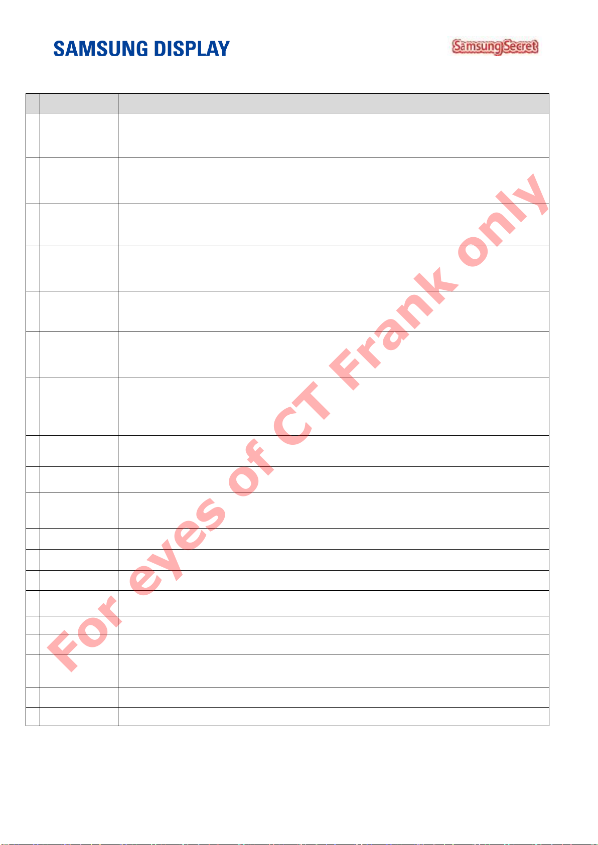
10. SPECIAL PRECAUSTIONS
——————————————————————————————————————————————––—
Doc.No. LSC400HM06-T Page 27 of 37 Rev.No. 06-000-G-20130404
Page 28
————————————————————————————————————————————————–
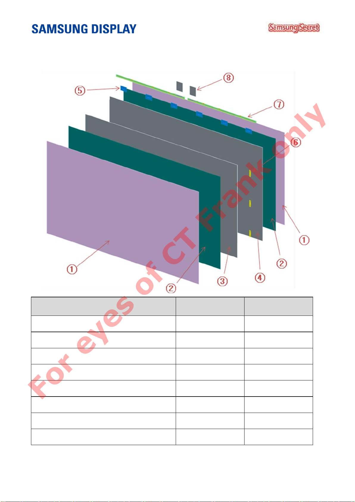
APPENDIX – RECOMMENDATION FOR THE BLU DESIGN
1. The schematic of panel
Item
Symbol
Remark
Protector Film
①
Removable
Polaroid Film
②
Color Filter Glass
③
TFT Glass
④
Source IC
⑤
Gate IC
⑥
Source PBA
⑦
FFC
⑧
For eyes of CT Frank only
——————————————————————————————————————————————––—
Doc.No. LSC400HM06-T Page 28 of 37 Rev.No. 06-000-G-20130404
Page 29
————————————————————————————————————————————————–
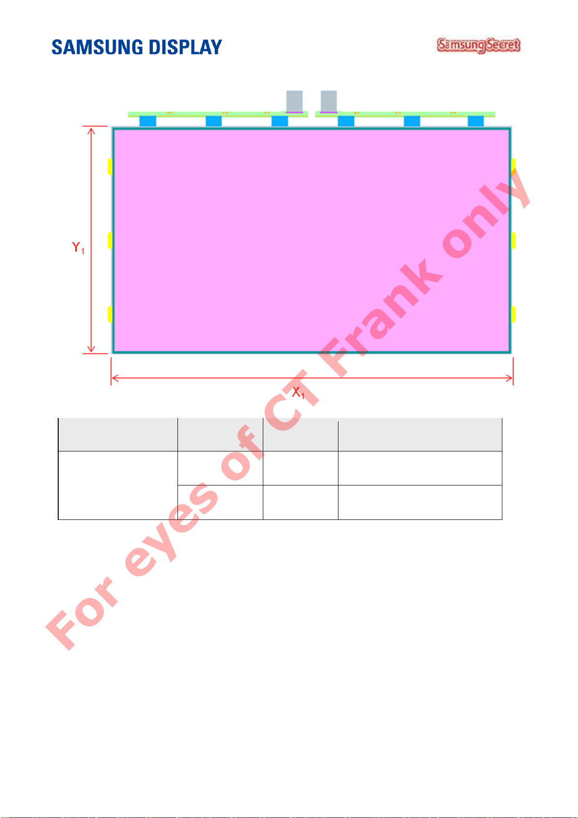
2. The tolerance of panel assembly
Item
Symbol
Min.
Note
Glass Cutting
X1
± 0.3
Y1
± 0.3
For eyes of CT Frank only
——————————————————————————————————————————————––—
Doc.No. LSC400HM06-T Page 29 of 37 Rev.No. 06-000-G-20130404
Page 30
————————————————————————————————————————————————–
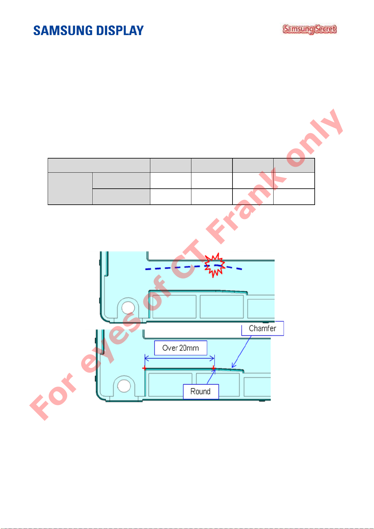
3. The guide for the mechanical design
3.1 The panel guide
(a) It is recommended to avoid the following cases since the light leakage can be caused by the
pressure of the guiding structure.
When the guiding part is made of plastic resin, the gap between the panel and the guiding structure
should be considered when you design. The shrinkage under the situation which the temperatures
change causes the light leakage. For your reference, it is recommended to have a total gap between
the panel and the guide structure as below (When the resin is composed of the PC and the 15% of
G/F.)
tꀀሄ
32”
40”
46”
55”
Total Gap
Right & Left
0.9
0.9
1.0
1.1
Top & Bottom
0.6
0.7
0.8
0.9
It is recommended to follow the dimension and the shape of the guiding structure stated as below
since the distortion of guiding parts can cause the light leakage
For eyes of CT Frank only
——————————————————————————————————————————————––—
Doc.No. LSC400HM06-T Page 30 of 37 Rev.No. 06-000-G-20130404
Page 31
————————————————————————————————————————————————–
For eyes of CT Frank only
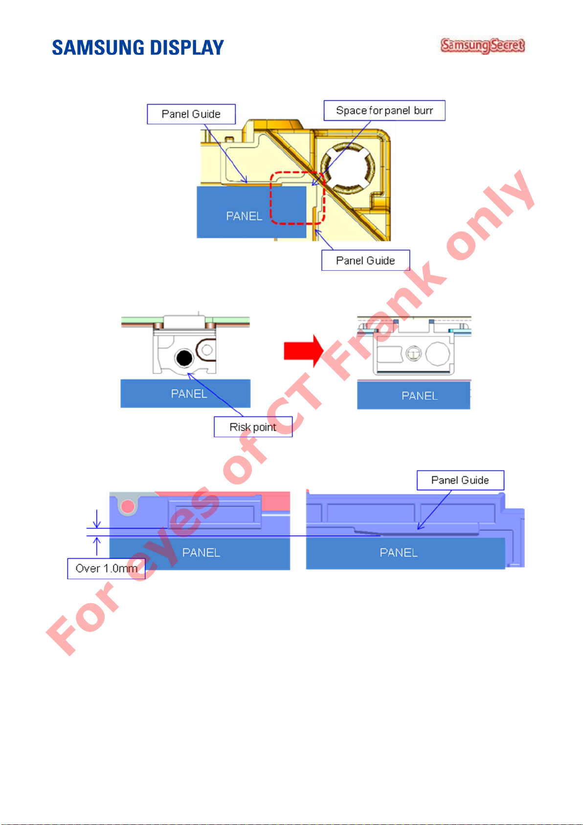
(b) When the panel guide point is designed at the edge of the panel, the points in the corner
shall not be designed to be contacted with the other parts in order to avoid the crack on the
panel caused by the burr of the panel.
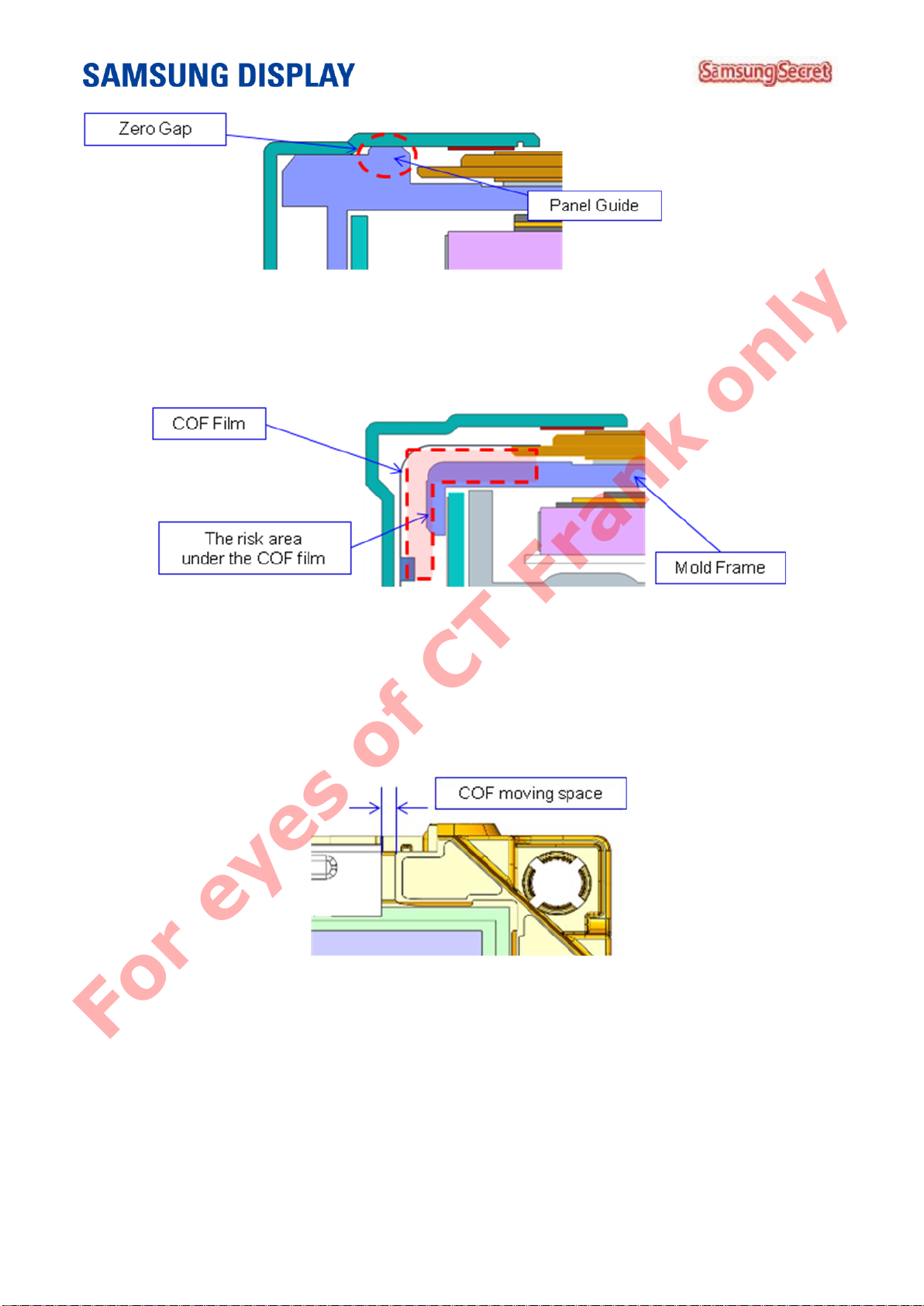
(c) It is recommended to avoid placing the ribs as shown below since the panel damage with
the unstable design can be easily happened under the external force.
-. The sharp or the round shape near the panel shall be changed to a flat shape, such as the
shape of screw point, the gate point, and etc.
-. It is recommended to keep the gap between the panel guides and ribs over 1mm in the
worst conditions.
(※ The suggested dimension does not guarantee the quality of the products.)
-. The gap between the panel guide and the front cover (or the front chassis) should be a
zero in Z-direction to avoid the being broken in the panel caused by being stuck between
the gap.
——————————————————————————————————————————————––—
Doc.No. LSC400HM06-T Page 31 of 37 Rev.No. 06-000-G-20130404
Page 32
————————————————————————————————————————————————–
3.2 The COF and the Drive IC
(a) The pattern of COF is easily damaged by the sharp edge of the press and the burr of
mold under the condition which the products are shaking while delivering. Therefore, it
is recommended to avoid designing not to locate the gate of mold or the parting line in
the position of COF when designing the product.
(b) It is recommended to secure the sufficient gap between the COF and the other parts when
designing the product since the lack of gap between the COF and the other parts can cause
the damage in the COF such as the lead crack under the condition which the product is
twisted.
(※ The space over 3.0mm for moving is recommended, but the quality of products is not
guaranteed.)
(c) The temperature of the surface of Drive-IC should be less than 100℃
For eyes of CT Frank only
——————————————————————————————————————————————––—
Doc.No. LSC400HM06-T Page 32 of 37 Rev.No. 06-000-G-20130404
Page 33
————————————————————————————————————————————————–
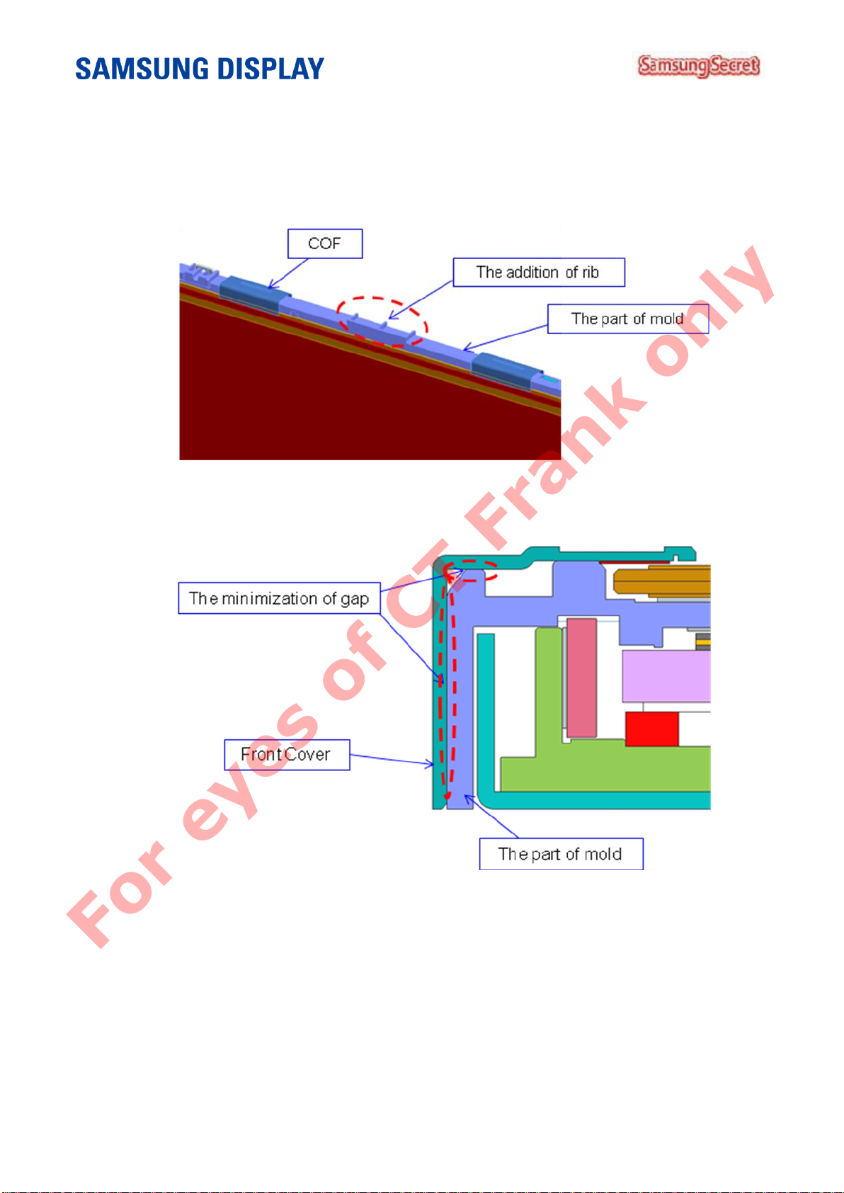
(d) The sufficient space for the COF and the Drive IC should be prepared including the worst
condition to prevent the damage on Drive-IC from the external force.
-. If the panel is placed to the upper part of the mold, it is recommended to keep the gap
between the mold and the front cover or the mold and the top chassis by adding the rib
between the COF and COF.
-. Design the gap between the rib and the cover to maintain the space for the protection of COF
as small as possible
For eyes of CT Frank only
——————————————————————————————————————————————––—
Doc.No. LSC400HM06-T Page 33 of 37 Rev.No. 06-000-G-20130404
Page 34
————————————————————————————————————————————————–
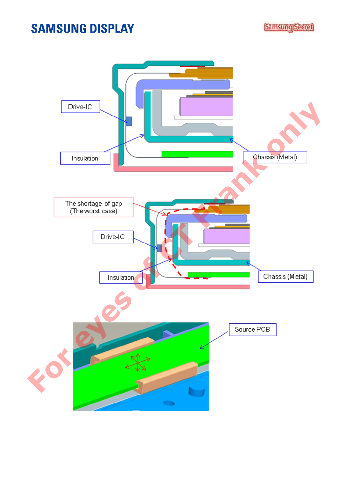
(e) When metal parts are assembled next to the Drive-IC, the metal part should be insulated to
avoid the damage on IC from the static electricity.
(f) If the length of COF is designed to be short, the lead crack can be occurred by applying the
tension on the COF due to the being shaking of the product.
(g) It is recommended to design source PCB can be easily moved to the direction of each axis in
order for the tension not to be applied to the edge of COF under vibrating condition, such as
transportation of the product.
For eyes of CT Frank only
——————————————————————————————————————————————––—
Doc.No. LSC400HM06-T Page 34 of 37 Rev.No. 06-000-G-20130404
Page 35
————————————————————————————————————————————————–
3.3 The control PBA and the Source PBA
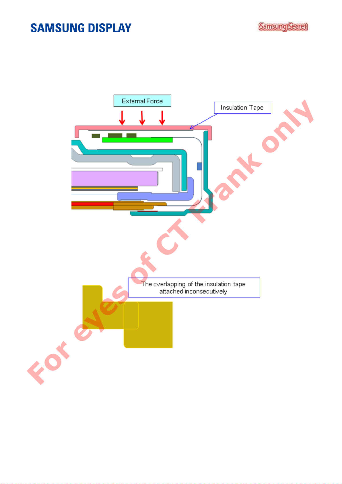
(a) The gaps between the source PBA and the other parts and the control PBA and other parts
should be considered to avoid the damage on electrical parts by the static electricity and the
external forces. If the material of shielding part is metal, the insulation method is
recommended.
(b) Confirm the status of insulation tape since the inappropriately attached insulation tape can
cause the damage on the parts of product if the insulation tape for the insulation of part of
PBA is attached inconsecutively due to the inappropriate design or the error occurred during
the process.
For eyes of CT Frank only
——————————————————————————————————————————————––—
Doc.No. LSC400HM06-T Page 35 of 37 Rev.No. 06-000-G-20130404
Page 36
————————————————————————————————————————————————–
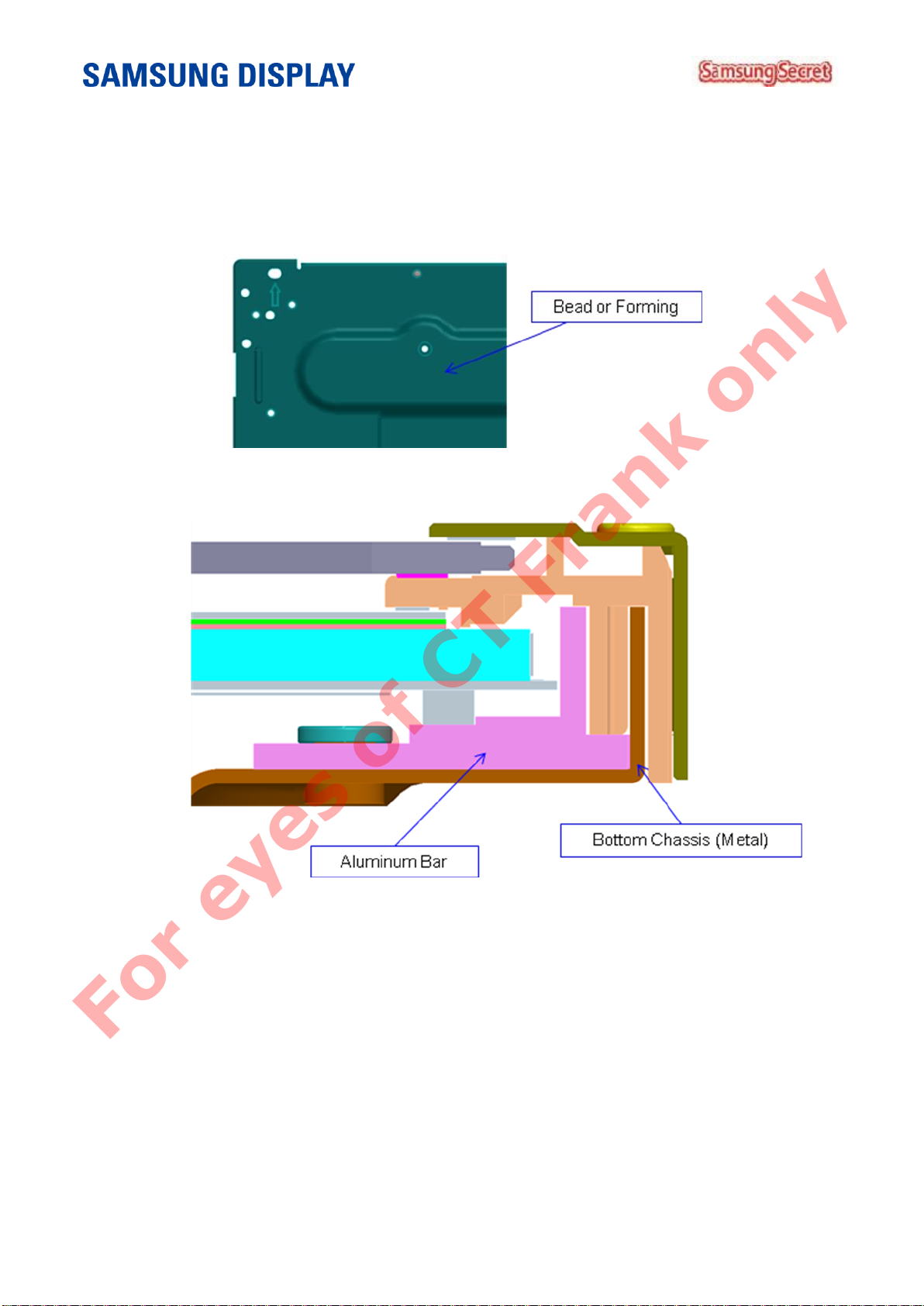
3. 4 The 4-Corner and the cloudy light leakage
(a) It is recommended to follow the method delineated in the picture below for designing
since the distortion on panel and the sharp increase of the temperature gradient in the
surface of panel can cause the light leakage.
-. Place the strong beads at the corner point to control the flatness of the panel.
-. The heat sinking plane in the lower parts shall contact with the bottom chassis.
For eyes of CT Frank only
——————————————————————————————————————————————––—
Doc.No. LSC400HM06-T Page 36 of 37 Rev.No. 06-000-G-20130404
Page 37

————————————————————————————————————————————————–
3.5 Others
(a) The corrosion of the source PBA
Be cautious when selecting the specification of tape or designing the product since the
corrosion of the parts of circuit caused by the overuse of the glass cleaner of the end user
may cause the occurrence of the abnormalities in the screen, if the model is the reversed
product which has the source PBA designed at the 90˚.
(b) The deterioration of crystal liquid
It is recommended to design the products to make the temperature of the active area of the
product operated below the 50℃ for the protection from containing the abnormalities in the
screen due to the deterioration of the liquid crystal. In addition, it is recommended to design the
product not to cause the occurrence of the deterioration of liquid crystal under the ambient
temperature of 50 ℃.
For eyes of CT Frank only
——————————————————————————————————————————————––—
Doc.No. LSC400HM06-T Page 37 of 37 Rev.No. 06-000-G-20130404
 Loading...