

Page 1
SERVICE
Manual
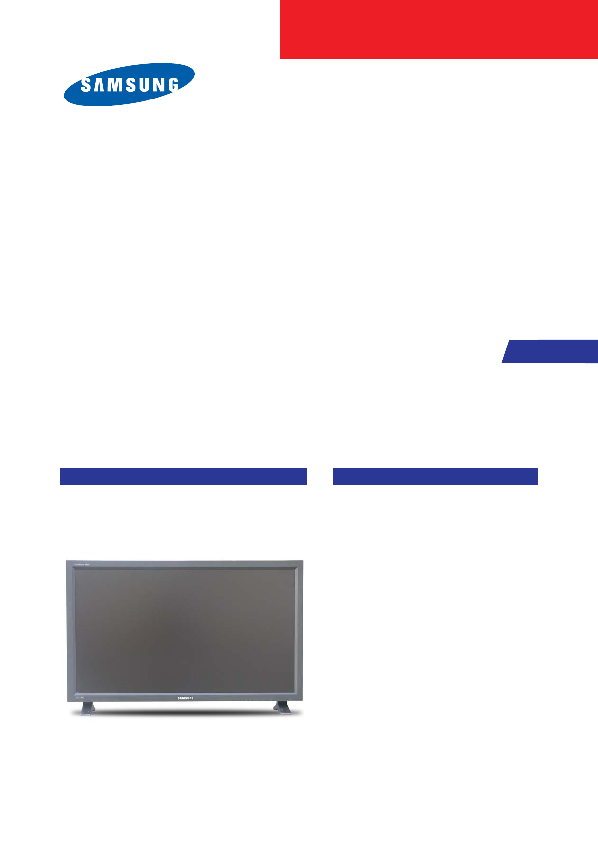
TFT-LCD Monitor Feature
LCD-Monitor
Chassis Model
LS32BHP 320PX
▶ VMB (Vertical Marketing Business) Model
▶ MFM (Multi Function Monitor) :
Compatible with various sources including PC (DVI,
AV, S-video, Component)
▶ Adopting Response Time 8ms SPVA
▶ SRS Trusurround supplied
▶ RS232 Remote Control
(MDC software supplied)
▶ Video Input : PC(D_SUB,DVI), BNC, DVI,
Component, AV, S-Video
▶ Audio Input : PC(D_SUB,DVI) Stereo, Video
(AV, S-Video) , Component, BNC
▶ Video & Audio Output : PC, BNC, AV, S-Video,
Component Output, Speaker Output
▶ 10W x 2 External Speaker
▶ PIP On timer function : The PIP automatically pops up
after the time setting
▶ PIP, OSD Menu Transparency Adjustment
▶ Off timer function
▶ Wall & Ceiling Mounting
(Optional VESA Wall Mount Kit)
Page 2

ii
Copyright
ⓒ 2006 by Samsung Electronics Co., Ltd.
All rights reserved.
This manual may not, in whole or in part, be copied,
photocopied, reproduced, translated, or converted to any
electronic or machine readable form without prior
written permission of Samsung Electronics Co., Ltd.
LS32BHP Service Manual
First edition October 2006.
Printed in Korea.
Trademarks
Samsung is the registered trademark of Samsung
Electronics Co., Ltd.
LS32BHP and Macmaster Cable Adapter are
trademarks of Samsung Electronics Co., Ltd.
Macintosh and Power Macintosh are trademarks of
Apple Computer, Inc.
All other trademarks are the property of their respective
owners.
Page 3

Contents
11. Precautions
……………………………………………………………………………………………………………………
11-1
1-1 Safety Precautions ……………………………………………………………………………………………………… 1-1
1-2 Servicing Precautions…………………………………………………………………………………………………… 1-2
1-3 Electrostatically Sensitive Devices (ESD) Precautions……………………………………………………………… 1-2
2
2. Product specifications
…………………………………………………………………………………………………………
22-1
2-1 Development Background ……………………………………………………………………………………………… 2-1
2-2 Fashion Feature ………………………………………………………………………………………………………… 2-1
2-2 Specifications …………………………………………………………………………………………………………… 2-2
2-3 Spec Comparison to the Old Models ………………………………………………………………………………… 2-3
2-4 Accessories ……………………………………………………………………………………………………………… 2-4
2-5 Accessories(Sold Separately) ………………………………………………………………………………………… 2-6
3
3. Alignment and Adjustments
…………………………………………………………………………………………………
33-1
3-1 Service Mode …………………………………………………………………………………………………………… 3-1
3-2 Service Mode Menu …………………………………………………………………………………………………… 3-2
3-3 DDC Input Process ……………………………………………………………………………………………………… 3-8
3-4 MDC(Multi Display Control) Program ………………………………………………………………………………… 3-10
3-5 MDC(Multi Display Control) Program_How to use ………………………………………………………………… 3-12
3-6 Updating the program - MAIN ………………………………………………………………………………………… 3-22
4
4. Troubleshooting
………………………………………………………………………………………………………………
44-1
4-1
No Power ………………………………………………………………………………………………………………… 4-1
4-2 No PC(D-SUB) Video …………………………………………………………………………………………………… 4-3
4-3 No DVI Video …………………………………………………………………………………………………………… 4-5
4-4
No BNC Video …………………………………………………………………………………………………………… 4-7
4-5
No Component Video …………………………………………………………………………………………………… 4-9
4-6
No Component Video ………………………………………………………………………………………………… 4-11
4-7 Program Upgrading - MAIN …………………………………………………………………………………………… 4-13
4-8 What To Do after Board Replacement ……………………………………………………………………………… 4-19
5
5. Exploded View & Parts List
……………………………………………………………………………………………………
55-1
5-1 Exploded View …………………………………………………………………………………………………………… 5-1
5-2 Parts List ………………………………………………………………………………………………………………… 5-2
6
6. Electrical Parts List
……………………………………………………………………………………………………………
66-1
6-1 Parts List ………………………………………………………………………………………………………………… 6-1
Page 4

Contents
77. Block Diagram
…………………………………………………………………………………………………………………
77-1
7-1 Main Block …………………………………………………………………………………………………………………7-1
7-2
SMPS Board ……………………………………………………………………………………………………………… 7-3
8
8. Wiring Diagram
…………………………………………………………………………………………………………………
88-1
8-1 Main Board Wiring Diagram ……………………………………………………………………………………………8-1
9
9. Schematic Diagram
……………………………………………………………………………………………………………
99-1
9-1 Main board Schematics Diagram(Signal input) ………………………………………………………………………9-1
9-2 Main board Schematics Diagram(SOUND) ……………………………………………………………………………9-2
9-3 Main board Schematics Diagram(SCALER)……………………………………………………………………………9-3
9-4 Main board Schematics Diagram(Power & Tuner Option) ……………………………………………………………9-4
9-8 Sub power Schematics Diagram ………………………………………………………………………………………9-8
1
10. Operating Installations and Installation
…………………………………………………………………………………
110-1
10-1 Front …………………………………………………………………………………………………………………… 10-1
10-2 Installing Stand Kit …………………………………………………………………………………………………… 10-8
1
11. Disassembly and Reassembly
……………………………………………………………………………………………
111-1
11-1 Disassembly …………………………………………………………………………………………………………… 11-1
11-2 Reassembly …………………………………………………………………………………………………………… 11-4
1
12. PCB Diagrams
………………………………………………………………………………………………………………
112-1
12-1 Main PCB layout ……………………………………………………………………………………………………… 12-1
12-2 SMPS Board layout ………………………………………………………………………………………………… 12-2
1
13 Circuit Descriptions
…………………………………………………………………………………………………………
113-1
13-1 Main board part ……………………………………………………………………………………………………… 13-1
1
14 Reference Infomation
………………………………………………………………………………………………………
114-1
14-1 Set UP ………………………………………………………………………………………………………………… 14-1
14-2 Terms…………………………………………………………………………………………………………………… 14-7
14-3 Timing Chart …………………………………………………………………………………………………………… 14-9
14-4 Preset Timing Modes ……………………………………………………………………………………………… 14-14
14-5 Panel Description …………………………………………………………………………………………………… 14-15
Page 5

Samsung Electronics Co.,Ltd.
416, Maetan-3Dong, Yeongtong-Gu, Suwon City, Gyeonggi-Do,
Korea, 443-742
Printed in Korea
P/N : BN82-00135J-00
URL : http://itself.sec.samsung.co.kr/
-This Service Manual is a property of
Samsung Electronics Co., Ltd.
Any unauthorized use of Manual can be
punished under applicable International
and/or domestic law.
Page 6

1 Precautions
1-1
1-1-1 Warnings
1. For continued safety, do not attempt to modify the circuit
board.
2. Disconnect the AC power and DC power jack before
servicing.
1-1-2
Ser vicing the LCD Monitor
1. When servicing the LCD Monitor, Disconnect the AC
line cord from the AC outlet.
2. It is essential that service technicians have an accurate
voltage meter available at all times. Check the
calibration of this meter periodically.
1-1-3 Fire and Shock Hazard
Before returning the monitor to the user, perform the
following safety checks:
1. Inspect each lead dress to make certain that the leads are
not pinched or that hardware is not lodged between the
chassis and other metal parts in the monitor.
2. Inspect all protective devices such as nonmetallic control
knobs, insulating materials, cabinet backs, adjustment
and compartment covers or shields, isolation resistorcapacitor networks, mechanical insulators, etc.
3. Leakage Current Hot Check (Figure 1-1):
WARNING : Do not use an isolation
transformer during this test.
Use a leakage current tester or a metering system that
complies with American National Standards Institute
(ANSI C101.1, Leakage Current for Appliances), and
Underwriters Laboratories (UL Publication UL1410,
59.7).
Figure 1-1. Leakage Current Test Circuit
4. With the unit completely reassembled, plug the AC line
cord directly into a 120V AC outlet. With the unit’s AC
switch first in the ON position and then OFF, measure
the current between a known earth ground (metal water
pipe, conduit, etc.) and all exposed metal parts,
including: metal cabinets, screwheads and control shafts.
The current measured should not exceed 0.5 milliamp.
Reverse the power-plug prongs in the AC outlet and
repeat the test.
1-1-4 Product Safety Notices
Some electrical and mechanical parts have special safetyrelated characteristics which are often not evident from visual
inspection. The protection they give may not be obtained by
replacing them with components rated for higher voltage,
wattage, etc. Parts that have special safety characteristics are
identified by on schematics and parts lists. A substitute
replacement that does not have the same safety characteristics
as the recommended replacement part might create shock, fire
and/or other hazards. Product safety is under review
continuously and new instructions are issued whenever
appropriate.
1 Precautions
Follow these safety, servicing and ESD precautions to prevent damage and to protect against potential hazards such as electrical shock.
1-1 Safety Precautions
Page 7

1 Precautions
1-2
1-2-1 General Ser vicing
Precautions
1. Always unplug the unit’s AC power cord from the AC
power source and disconnect the DC Power Jack before
attempting to:
(a) remove or reinstall any component or assembly, (b)
disconnect PCB plugs or connectors, (c) connect a test
component in parallel with an electrolytic capacitor.
2. Some components are raised above the printed circuit
board for safety. An insulation tube or tape is sometimes
used. The internal wiring is sometimes clamped to
prevent contact with thermally hot components. Reinstall
all such elements to their original position.
3. After servicing, always check that the screws,
components and wiring have been correctly reinstalled.
Make sure that the area around the serviced part has not
been damaged.
1. Immediately before handling any semiconductor
components or assemblies, drain the electrostatic charge
from your body by touching a known earth ground.
Alternatively, wear a discharging wrist-strap device. To
avoid a shock hazard, be sure to remove the wrist strap
before applying power to the monitor.
2. After removing an ESD-equipped assembly, place it on a
conductive surface such as aluminum foil to prevent
accumulation of an electrostatic charge.
3. Do not use freon-propelled chemicals. These can
generate electrical charges sufficient to damage ESDs.
4. Use only a grounded-tip soldering iron to solder or
desolder ESDs.
5. Use only an anti-static solder removal device. Some
solder removal devices not classified as “anti-static” can
generate electrical charges sufficient to damage ESDs.
4. Check the insulation between the blades of the AC plug
and accessible conductive parts (examples: metal panels,
input terminals and earphone jacks).
5. Insulation Checking Procedure: Disconnect the power
cord from the AC source and turn the power switch ON.
Connect an insulation resistance meter (500 V) to the
blades of the AC plug.
The insulation resistance between each blade of the AC
plug and accessible conductive parts (see above) should
be greater than 1 megohm.
6. Always connect a test instrument’s ground lead to the
instrument chassis ground before connecting the positive
lead; always remove the instrument’s ground lead last.
6. Do not remove a replacement ESD from its protective
package until you are ready to install it. Most
replacement ESDs are packaged with leads that are
electrically shorted together by conductive foam,
aluminum foil or other conductive materials.
7. Immediately before removing the protective material
from the leads of a replacement ESD, touch the
protective material to the chassis or circuit assembly into
which the device will be installed.
Caution:Be sure no power is applied to the
chassis or circuit and observe all
other safety precautions.
8. Minimize body motions when handling unpackaged
replacement ESDs. Motions such as brushing clothes
together, or lifting your foot from a carpeted floor can
generate enough static electricity to damage an ESD.
1-3 Static Electricity Precautions
Some semiconductor (solid state) devices can be easily damaged by static electricity. Such components are commonly called
Electrostatically Sensitive Devices (ESD). Examples of typical ESD are integrated circuits and some field-effect transistors. The
following techniques will reduce the incidence of component damage caused by static electricity.
1-2 Ser vicing Precautions
WARNING: An electrolytic capacitor installed with the wrong polarity might explode.
Caution: Before servicing units covered by this service manual, read and follow the Safety Precautions section
of this manual.
Note: If unforeseen circumstances create conflict between the following servicing precautions and any of the safety
precautions, always follow the safety precautions.
Page 8

1 Precautions
1-3
1. For safety reasons, more than two people are
required for carrying the product.
2. Keep the power cord away from any heat emitting
devices, as a melted covering may cause fire or
electric shock.
3. Do not place the product in areas with poor
ventilation such as a bookshelf or closet. The
increased internal temperature may cause fire.
4. Bend the external antenna cable when connecting
it to the product. This is a measure to protect it
from being exposed to moisture. Otherwise, it
may cause a fire or electric shock.
5. Make sure to turn the power off and unplug the
power cord from the outlet before repositioning
the product. Also check the antenna cable or the
external connectors if they are fully unplugged.
Damage to the cord may cause fire or electric
shock.
6. Keep the antenna far away from any high-voltage
cables and install it firmly. Contact with the highvoltage cable or the antenna falling over may
cause fire or electric shock.
7. When installing the product, leave enough space
(10cm) between the product and the wall for
ventilation purposes.
A rise in temperature within the product may
cause fire.
1-4 Installation Precautions
Page 9

Memo
1 Precautions
1-4
Page 10

2. Product Specifications
2-1
2 Product specifications
2-1 Development Background
- Expansion of Wide LCD Product Market (Public facilities like airport, theater, etc.)
- Improving the picture quality and enhancing the extra features compatible to the current model
- Securing competitiveness with the strengthen Network Option and keeping up the user convenience
2-1-1 Fashion Feature
▶ VMB (Vertical Marketing Business) Model
▶ MFM (Multi Function Monitor) :
Compatible with various sources including PC (DVI, AV, S-video, Component)
▶ Adopting Response Time 8ms SPVA
▶ SRS Trusurround supplied
▶ RS232 Remote Control (MDC software supplied)
▶ Video Input : PC(D_SUB,DVI), BNC, DVI, Component, AV, S-Video
▶ Audio Input : PC(D_SUB,DVI) Stereo, Video (AV, S-Video) , Component, BNC
▶ Video & Audio Output : PC, BNC, AV, S-Video, Component Output, Speaker Output
▶ 10W x 2 External Speaker
▶ PIP On timer function : The PIP automatically pops up after the time setting
▶ PIP, OSD Menu Transparency Adjustment
▶ Off timer function
▶ Wall & Ceiling Mounting (Optional VESA Wall Mount Kit)
Page 11
2. Product Specifications
2-2
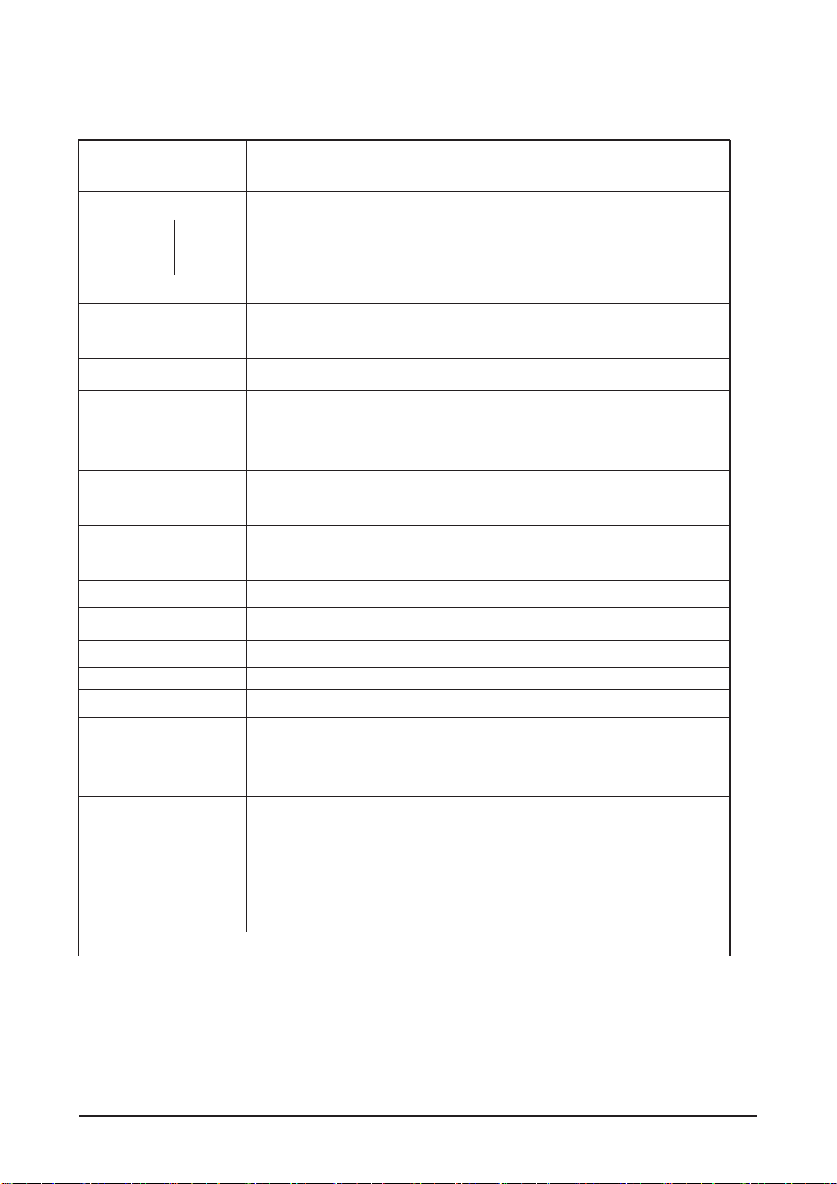
2-2 Specifications
Item Description
LCD Panel AMLCD 32" ( LTA320WT-L16 )
Scanning Horizontal 30~70kHz
Frequency Vertical 50~85Hz
Display Colors 16.7 Million colors
Maximum Horizontal 1366 Pixels
Resolution Vertical 768 Pixels
Input Video Signal 0.7 Vp-p ± 5% positive at 75Ω, Digital, TMDS internally terminated
Input Sync Signal Type :
separate H/V sync, Composite, automatic synchronization without external switch
Level : TTL level
Active Display
Horizontal/Vertical 871.68 ± 3 mm (H) / 523.008 ± 3 mm (V)
AC power voltage & Frequency
AC 90~264V, 60 Hz/50 Hz ± 3 Hz
Power Consumption(DPMS)
160W(w/o option), 5W(DPMS)
Brightness 450cd/m
2
Contrast Ratio 1200:1
Response Time 8 ms (by DDC2)
Range of vision angle
(Left/Right/UP/Down) 89˚/ 89˚/ 89˚/ 89˚
Video System AV, S-Video, Component
Sound Output Max.10W x 2ch
Dimensions (W x H x D)
Set 780 x 482 x 107 mm / 30.1 x 19.0 x 4.6 inch
780 x 530 x 223 mm / 30.1 x 20.9 x 8.8 inch
Weight (Set/Package) 16Kg (without Stand)
18Kg (with Stand)
Environmental Considerations
Operating Temperature : 50°F ~ 104°F (10℃ ~ 40℃)
Operating Humidity : 10% ~ 80%
Storage Temperature : -4°F ~ 113°F (-20℃ ~ 45℃)
Storage Humidity : 5% ~ 95%
-Designs and specifications are subject to change without prior notice.
PC Input D-SUB, DVI
Page 12
2. Product Specifications
2-3
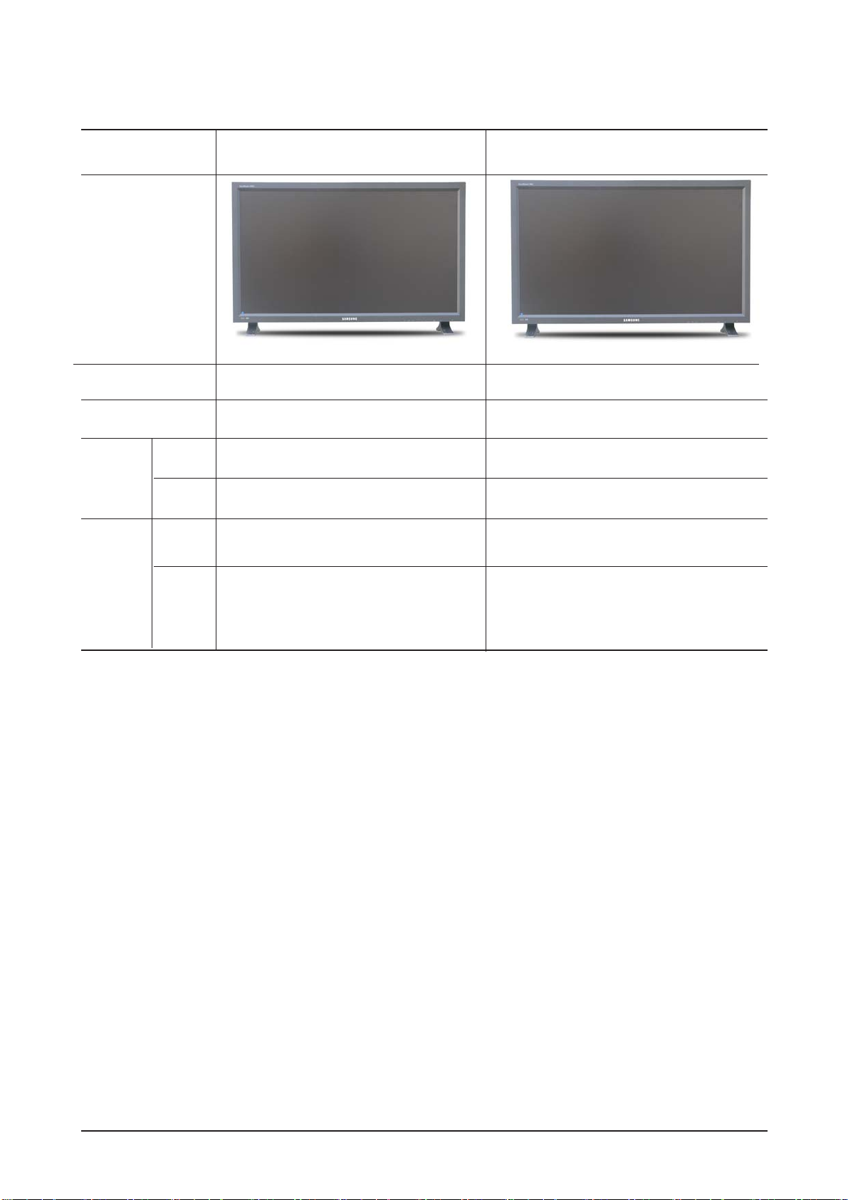
2-3 Spec Comparison to the Old Models
Model
Design
32"(1366x768),SPVA
450cd/m
2
, 1200 : 1, 178/178, 8ms
D-Sub, DVI-D, BNC
S-video, CVBS, Component
10 Watts x 2 ch
SRS Trusrround
.Power On Delay
.Network Option
.Safety Screen
.Monitor information (S/N)
.Video Wall
.MDC
.PIP/PBP, DNIe
.MDC Program
.VESA Wall Mount
.Remote Comtrol
10 Watts x 2 ch
VR Dolby, BBE
LS32BHP
Panel
Panel Spec.
Input
PC
Video
Speaker
Funtion
32"(1366x768), PVA
450cd/m
2
,
1000 : 1, 178/178, 8ms
D-Sub, DVI-D, BNC
S-video, CVBS, Component
LBE32PS
Page 13

2. Product Specifications
2-4
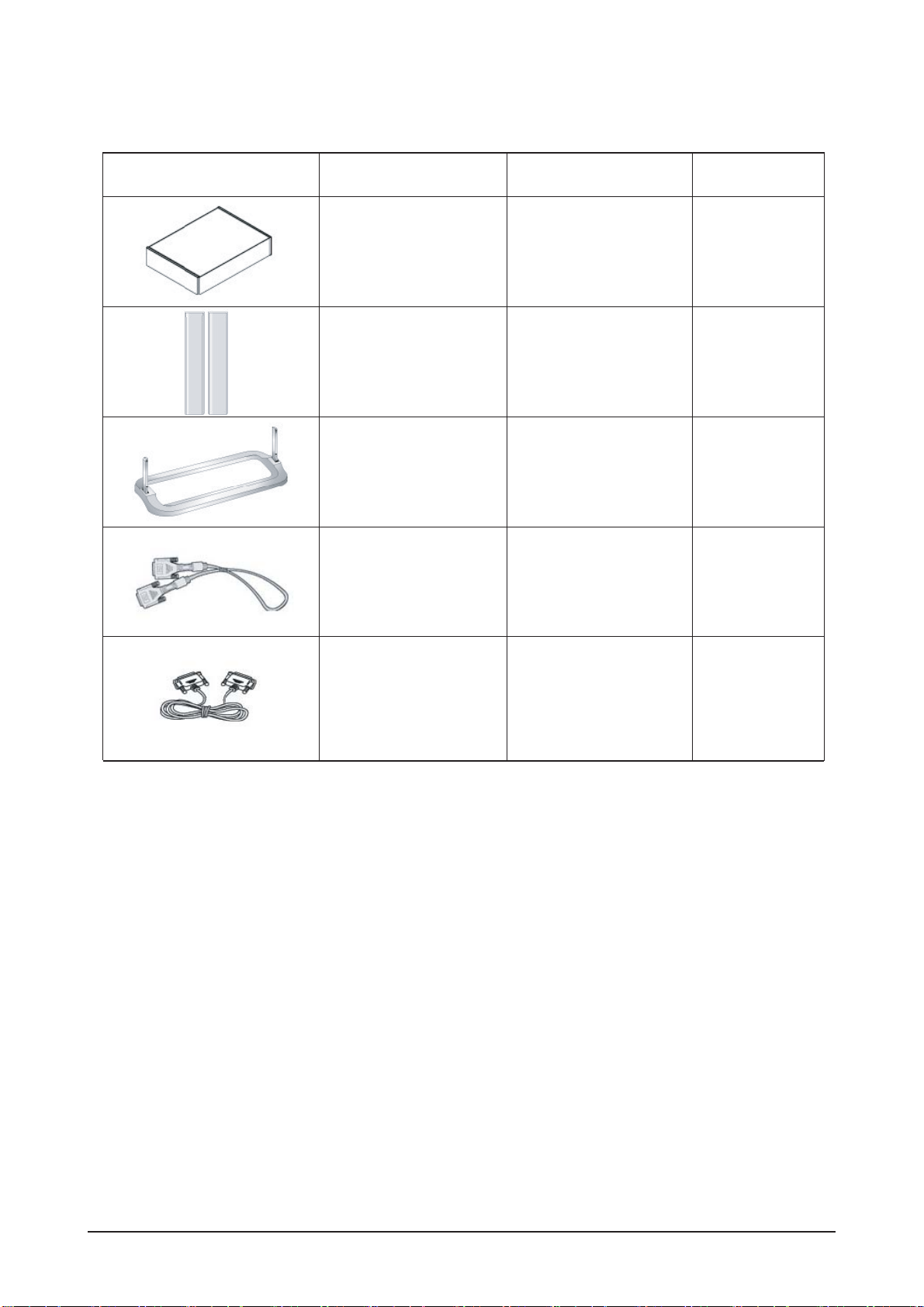
2-4 Accessories
Product Description
Quick Setup Guide
BN68-01021D
BH68-00527A
BN59-00528D
BN39-00244B
3903-000067
BN96-00452E
6003-001026
Warranty Card
(Not available in all
locations)
User's Guide,MDC
software, Natural Color
software, MagicNet
software
D-Sub(15 Pin)
Cable
Power Cord
Semi Stand
Screw (4EA)
TAPTITLE : M4 × L15
Ccde. No
Remark
3705-001262
BNC to RCA Adapter
Jack ×4
BN39-00530A
Speaker Wire Cable
Page 14

2. Product Specifications
2-5
Remote Control
BN59-00489A
4301-000121
BN96-00597D
Batteries (AAA x 2)
Cover-Hole
Product Description Ccde. No
Remark
Page 15
2. Product Specifications
2-6
2-5 Accessories(Sold Separately)
Wall mount KIT
Model:
WMB-4050P
BN96-01806A
BN96-00428C
BN39-00246F
Speaker Set
Stand KIT
DVI Cable
Product Description Ccde. No
Remark
BN39-00341A
RS232C Cable
Page 16
3. Alignment and Adjustments
3-1
3
Alignment and Adjustments
3-1 Ser vice Mode
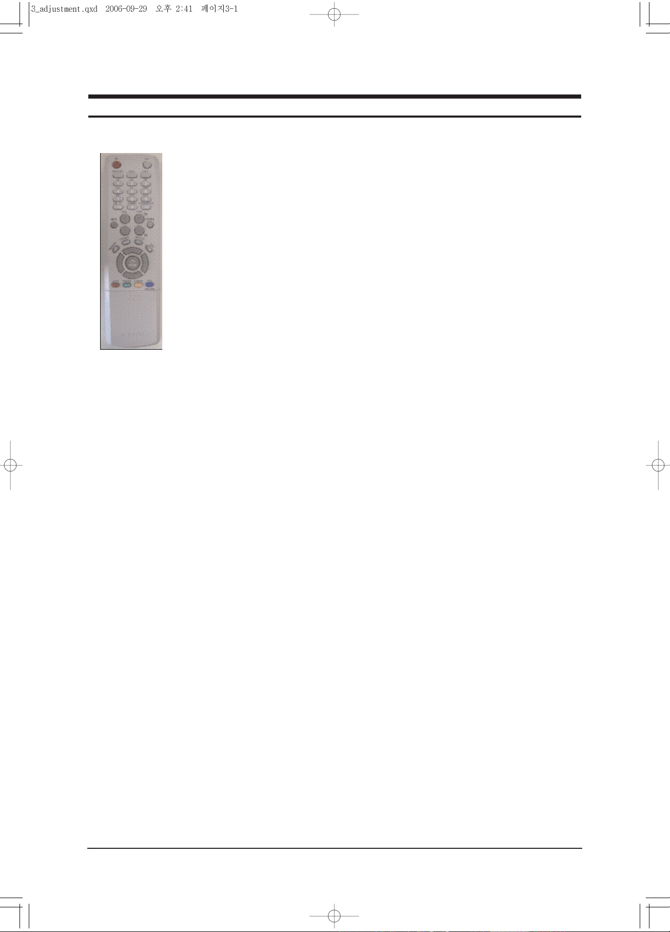
3-1-1 Entering the Factory menu on the Main board(using REMOCON)
- Power Off + MUTE + 1+ 8 + 2 + Power On
-When use the Factory remote control : INFO + Factory
Page 17
3. Alignment and Adjustments
3-2
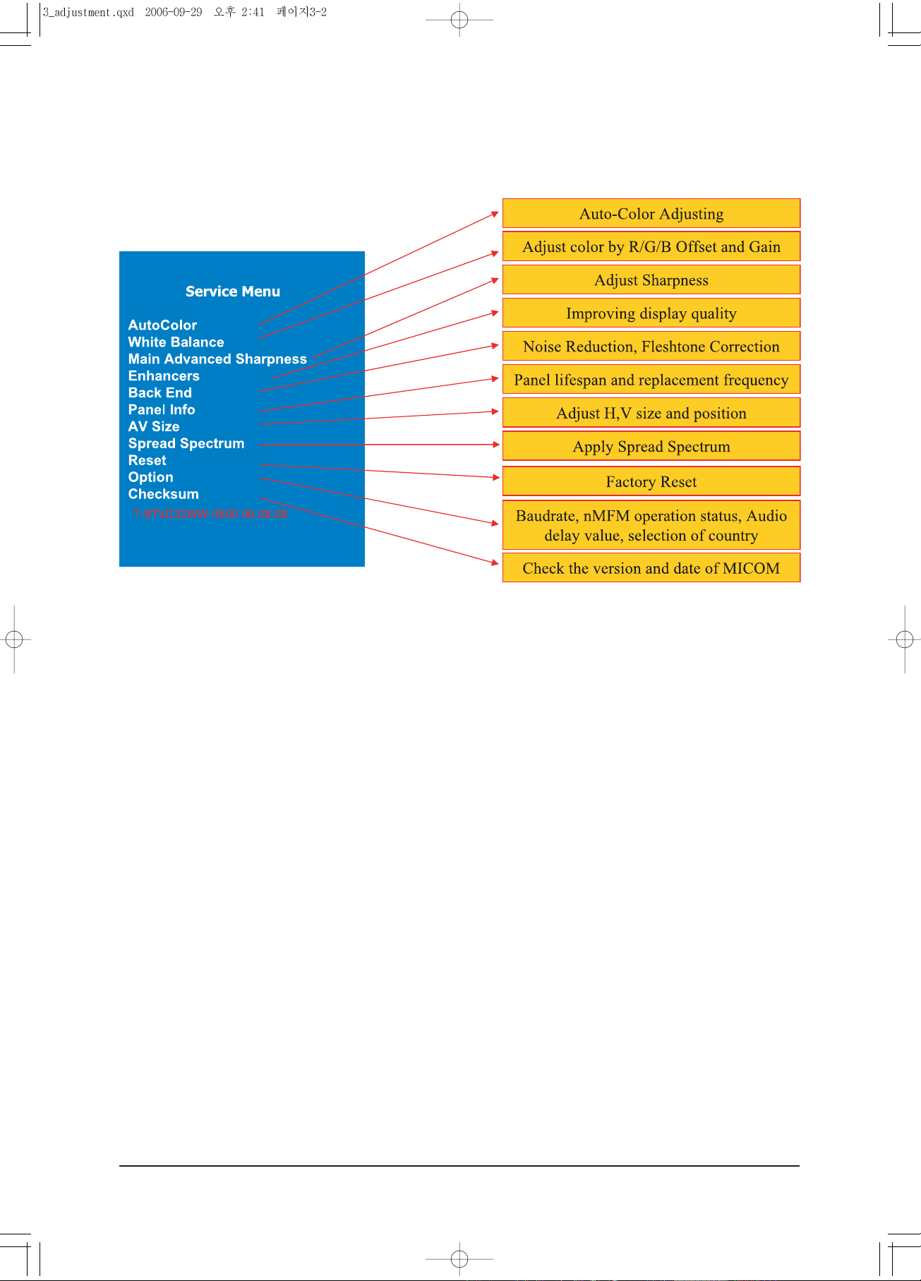
3-3 Ser vice Mode Menu
Page 18
3. Alignment and Adjustments
3-3
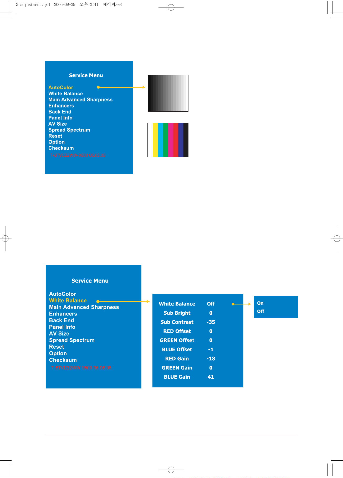
- AutoColor Part
PC analog Only ( 1024x768@60 16gray
pattern)
The Color Control properly operates only in
the certain pattern with certain mode and the
color warps in other patterns and modes.
Also the proper color control is not supported
in the mode other than XGA 60Hz.
Component ( 720p color bar pattern)
Color control operates normally only in certain modes
of certain patterns, but in other cases, the operation
may distort color.
Extreme caution needed.!!
- White Balance Par t
Register value in the Scaler
RED / BLUE / GREEN
Adjust the Gain and Offset
On: Display factory
adjusting value
Off: Display default
setting value
Used for color control.
But excessive setting may saturate the color.
Extreme caution needed.!!
Page 19
3. Alignment and Adjustments
3-4
- Sharpness Par t (1)
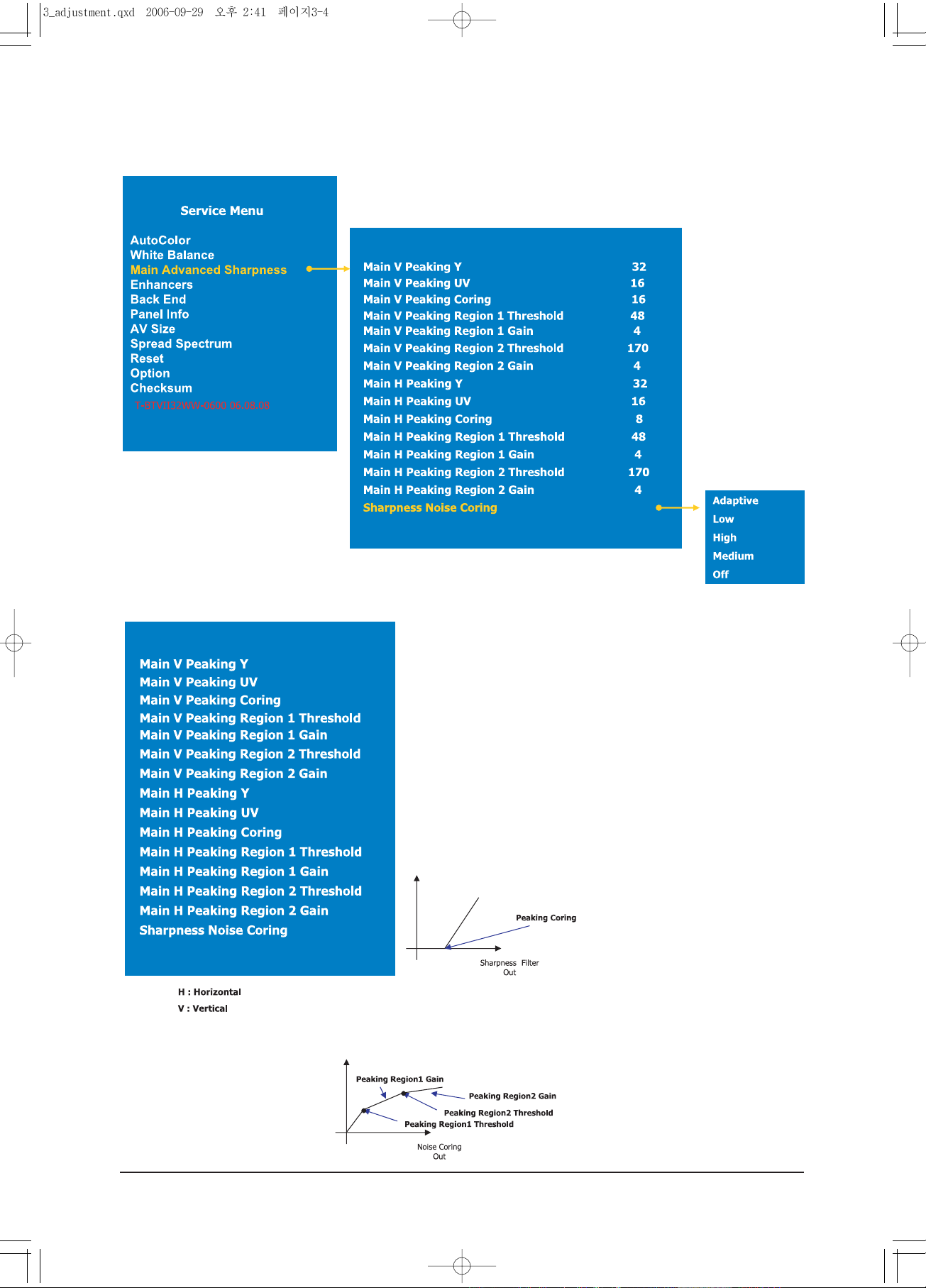
Adjusting the sharpness of displayed image.
- Sharpness Par t (2)
Scaling Filter Sharpness Control - Peaking Y / Peaking UV
This adjusts the sharpness of luminance(Y) and color(UV).
The bigger the number is in the range of 1~127, the clearer
the picture is. The bigger the number is in the range of
128~255, the more natural video is. Too high sharpness may
cause the vivid noise.
Noise Coring Control - Peaking Coring
Display only the sharp large-edge without assuming the smalledge of the video as a noise and amplifying it.
NonLinear Sharpness Control - Peaking Resion1/2 Threshold, Gain
Divide the frequency area and apply the different Gain for each area rather
than evenly apply the sharpness level over the whole image.
Assign the threshold value to
improve the sharpness.
Noise Coring Out
Nonlinear Out
Page 20
3. Alignment and Adjustments
3-5
- Enhancers Par t
Adjust to display the clear and sharp image.
This function is used to adjust the appropriate value for
each target region. Change only when it is needed.
HLE : Horizontal Large Edge Enhancer
HDP : Horizontal Detail Processor
HCE : Horizontal Chroma Enhancer
VDP : Vertical Detail Processor
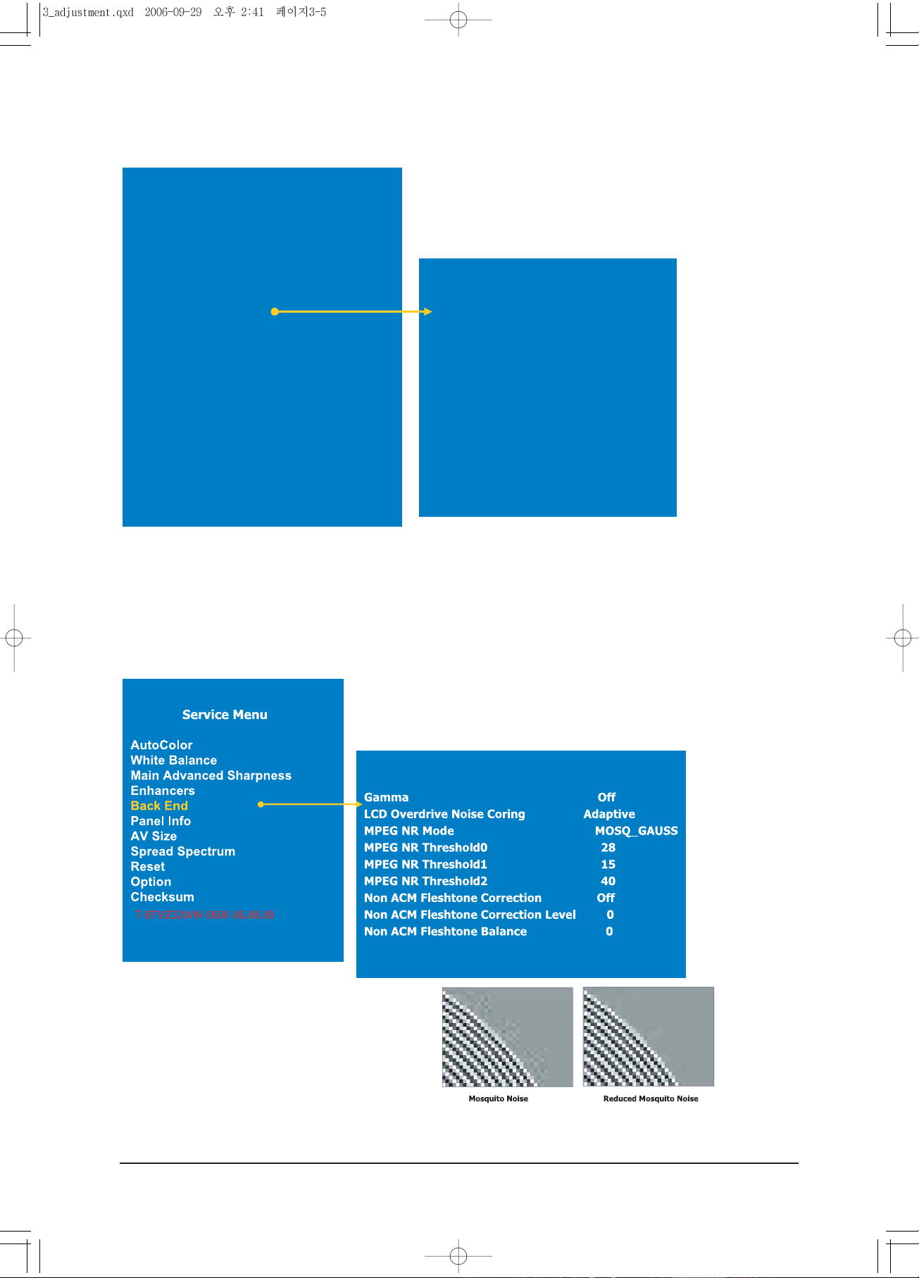
- Back End Part
The MPEG NR menu is used to reduce the Mosquito noise
and Gaussian noise. The Fleshtone menu is used to display
the natural skin color.
Service Menu
AutoColor
White Balance
Main Advanced Sharpness
Enhancers
Back End
Panel Info
AV Size
Spread Spectrum
Reset
Option
Checksum
T-BTVII32WW-0600 06.08.08
HLE Threshold
HLE Gain
HDP Threshold
HDP Gain
HCE Threshold
HCE Gain
VDP Threshold
VDP Gain
10
180
21
71
15
25
27
3
Page 21

3. Alignment and Adjustments
3-6
- Panel Info Part
Display the panel use time and the number of change.
Time Reset : Press the menu button on the front panel for 5 seconds.
- AV Size Part
AV size, position Adjustment
H,V size / H,V Position
Page 22
3. Alignment and Adjustments
3-7
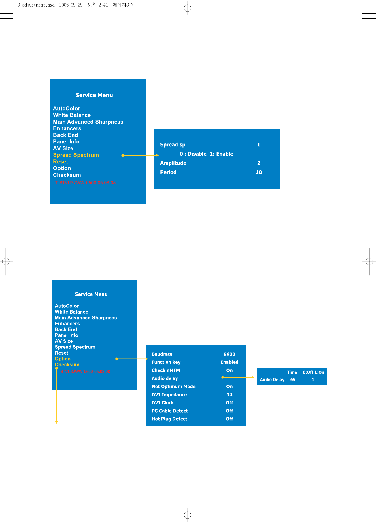
- Spread Spectrum/Reset Par t
Spread Spectrum Adjustment
The application status of Spread spectrum
Amplitude and Period Setting
Reset : Factory Reset
Reset the setting on the Service Menu to the default setting.
Need to turn the Power On/Off after reset
- Option/Checksum Part
Option Adjustment
Baudrate Speed Setting (The default value is 9600.
Change to 115200 when the code update on the main board is required.)
Function Key Setting/Unsetting
Option Setting in the Network part
Audio delay Setting (Set for the video and audio synchronization.)
The message display in the improper resolution mode Setting/Unsetting
DVI cable impedance matching setting
DVI clock reset Setting/Unsetting
PC cable detect Setting/Unsetting
DVI hot plug detect Setting/Unsetting
Checksum
The 4 digit serial number regarding the micom code is
displayed if you select this.
Page 23
3-4 DDC Input Process
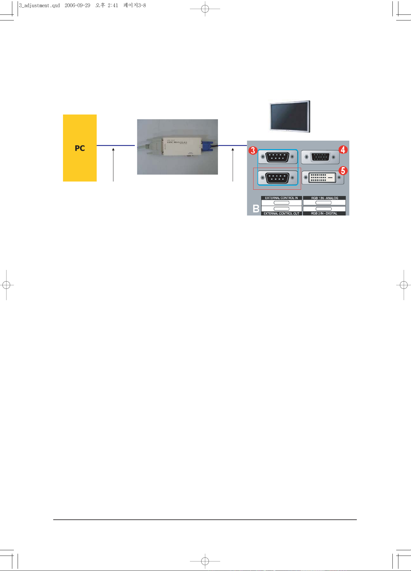
Connecting D-sub cable between the parallel port(printer port) of computer and Monitor.
3. Alignment and Adjustments
3-8
Connecting to the parallel
port of computer
Connecting to Monitor
Page 24

3. Alignment and Adjustments
3-9
- DDC Input Process
(DDC file name : SM320PXA1.DDC / SM320PXD1.DDC)
The DDC input is available after entering the Service Mode.: Cancel the DDC Protection.
1. Open the file.
2. Select Port 1 (D-SUB) / Select Port 2(DVI)
3. Select the DDC file.
4. Click the Next(OK) button.
5: Input the monitor serial number and press Enter.
Input Analog and repeat 2~5 times when input Digital.
5
Page 25
3. Alignment and Adjustments
3-10
3-5 MDC(Multi Display Control) Prog ram
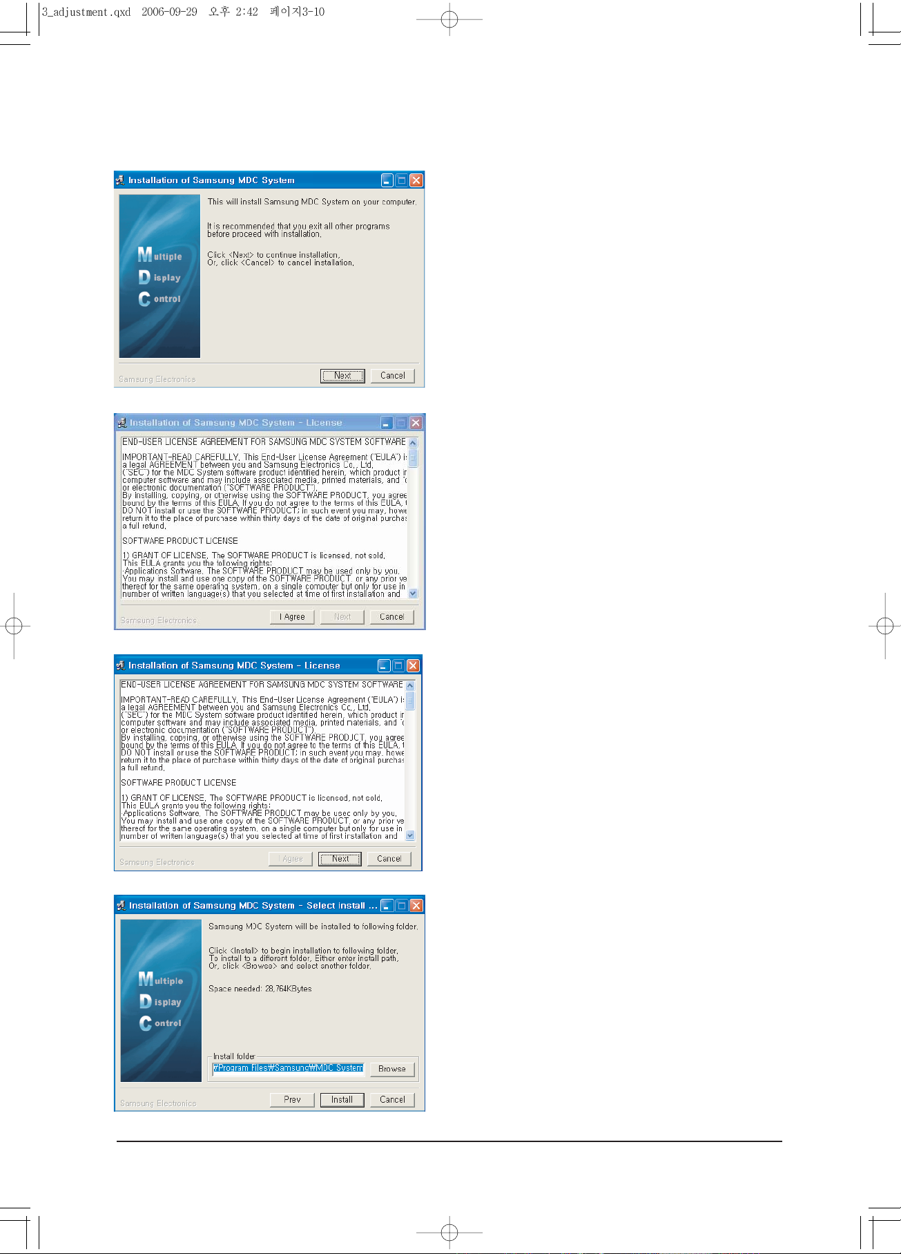
1. Run the SETUP. EXE file.
2. Select I Agree.
3. Select NEXT.
4. Select Install.
Page 26

3. Alignment and Adjustments
3-11
5. "Yes" Click.
6. "OK" Click.
Page 27
3. Alignment and Adjustments
3-12
3-6 MDC(Multi Display Control) Prog ram_How to use
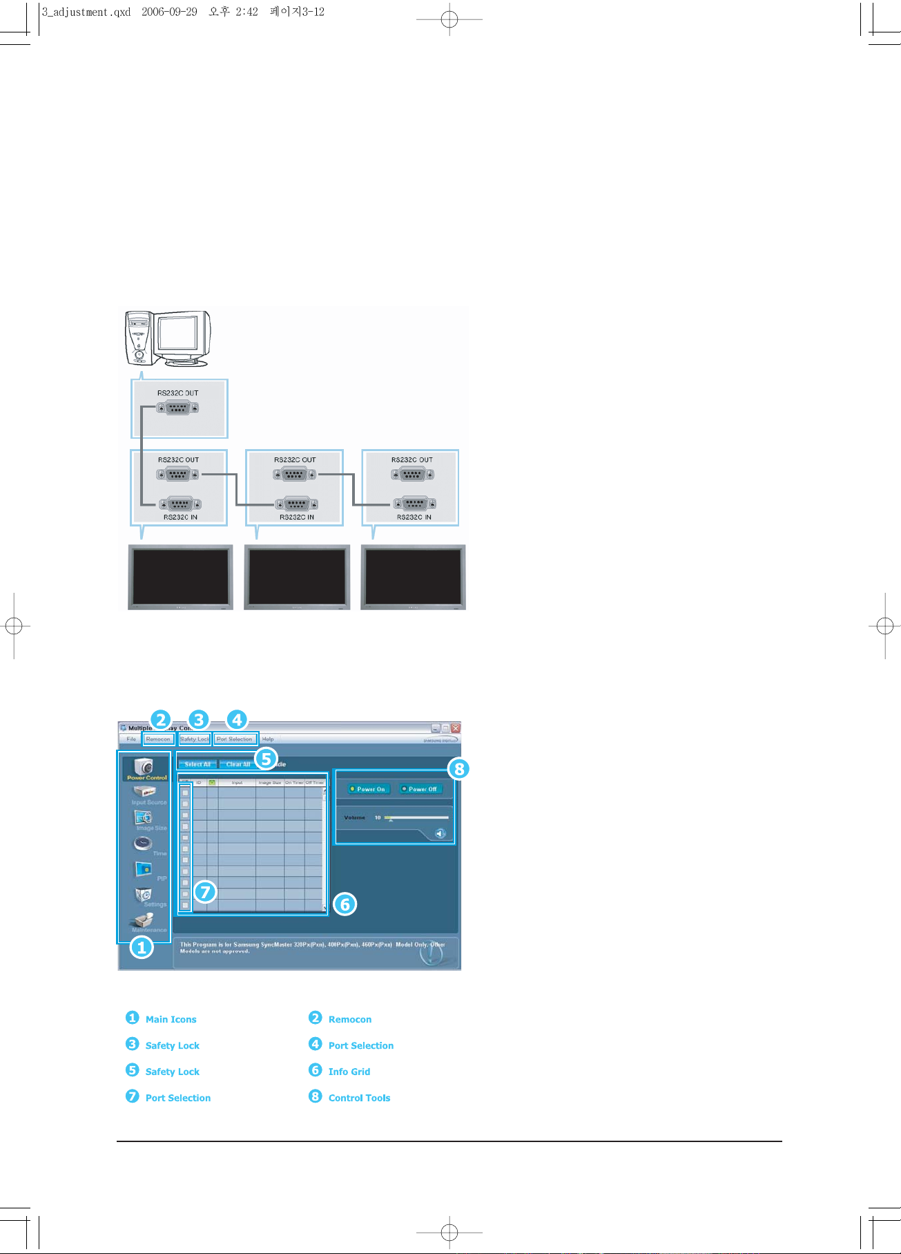
- Connect the serial port of the PC and Beethoven Board with the RS232C cable.
- Option in the Factory Menu : Check if BaudRate is set to 9600
A Multiple Display Control (MDC) is an application
allowing various displays to be easily and
simultaneously operated on a PC. RS-232C, a
standard of serial communication, is used for the
communication between a PC and a display.
Therefore, a serial cable should be connected
between the serial port on a PC and the serial port
on a display.
Refer to the diagram.
1. Click the main icons to switch into each
screen.
2. Allows you to enable or disable the remote
control signal receiving function of the display
unit.
3. Use to lock monitor functions.
4. Use to change the port. The default port is
COM1.
5. Use Select All and Clear All buttons to select
or clear all displays.
6. Use Grid to view brief information on selected
display.
The remote control Enable/Disable function
operates whether or not the power is On/Off,
and this applies to all displays connected to the
MDC. However, all displays return to the default
setting with the remote control receiving function
enabled regardless of the status at the time the
MDC is shut down
- Start- Main Window
Click Start > Program > Multiple Display Control to start the program.
Select a set to see the volume of the selected set within the slider.
Page 28

3. Alignment and Adjustments
3-13
1. Multiple Display Control is originally set to
COM1.
2. If the port other than COM 1 is used, any port
between COM1 to COM4 is selectable.
3. The port connected to the monitor and serial
cable needs to be assigned with the correct
name for the communications.
4. Once the port is selected, it is stored and
used for the next program.
- Start-Port Selection
1. Click Power Control of the main icons to display the
Power Control window.
- Info Grid shows some basic information necessary
for Power Control.
1) Power Status
2) Input Source
3) Image Size
4) On Timer Status
5) Off Timer Status
2. Use the Select All button or Check Box to choose a
display to control.
Power Control allows you to control functions
regarding the power of the selected display on the
menu.
6) Power On/Off
Turns the power of the selected display on or off.
7) Volume
Adjust the volume of the selected display.
The appropriate volume for the selected set is
displayed as you select a set.
(When you cancel the selection or choose Select
All, the volume returns to the default value 10.)
8) Mute On/Off
Turns on or off the Mute function of the selected
monitor. The Power Control feature is available for
all connected monitors.
- The Volume Control and Mute features are
available only for the displays whose power
status is ON.
- Power Control
1 2 3 4 5
6
7
8
Page 29
3. Alignment and Adjustments
3-14
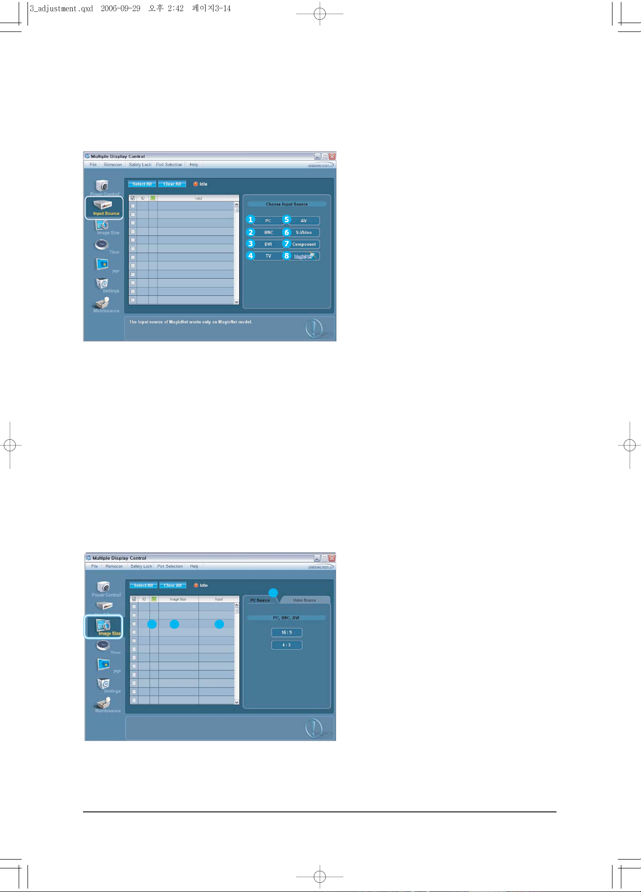
- Info Grid shows some basic information necessary to Input
Source Control.
1) PC
Changes the Input Source of the selected display to PC.
2) BNC
Changes the Input Source of the selected display to BNC.
3) DVI
Changes the Input Source of the selected display to DVI.
4) TV
Changes the Input Source of the selected display to TV.
5) AV
Changes the Input Source of the selected display to AV.
6) S-Video
Changes the Input Source of the selected display to
S-Video.
7) Component
Changes the Input Source of the selected display to
Component.
8) MagicNet
The MagicNet input can be changed only in the MagicNet
mode.
- The Input Source Control feature is available only for
the display whose power status is ON.
-Input Source Control
1. Click Input Source of the main icons to display the Input Source control window.
Click Select All or use Check Box to select a display to control.
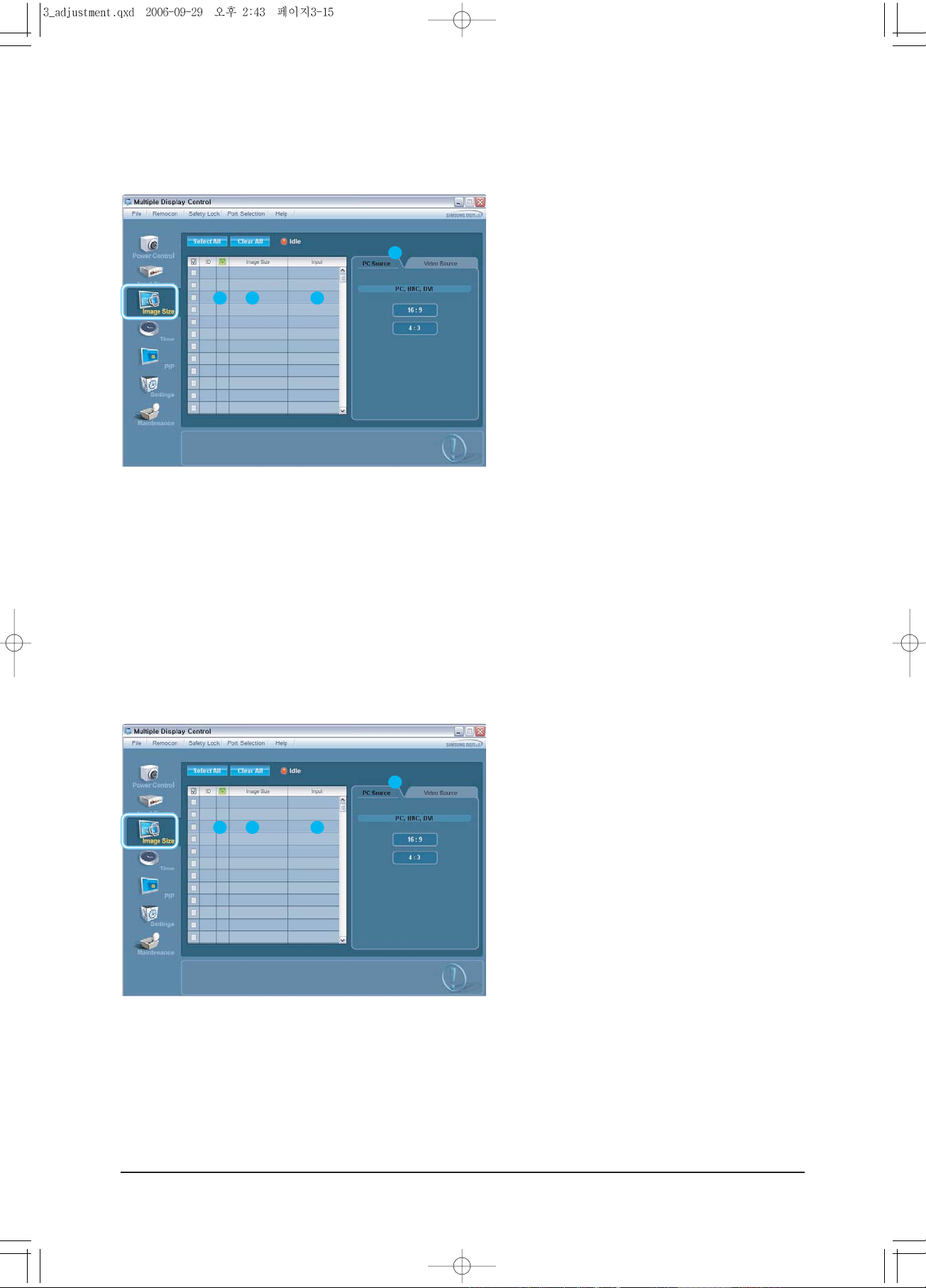
- Info Grid shows some basic information necessary to
Image Size Control.
1) Power
Shows the power status of the current display.
2) Image Size
Shows the current Image Size of the display in use.
3) Input Source
Shows the current Input Source of the display in use.
Info Grid displays only the displays whose Input Source is
PC, BNC, or DVI.
4) When you click Image Size, the PC, BNC, and DVI tabs
first appear.
This feature allows you to control Image Size for PC, BNC,
or DV.
- Image Size Control is available only for the displays
for whose power status is ON.
-Image Size Control - PC, BNC, DVI
1. Click Image Size of the main icons to display the Image Size control window.
4
1 2 3
Page 30
3. Alignment and Adjustments
3-15
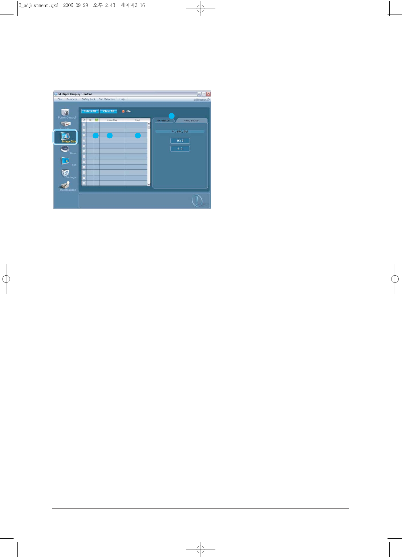
- Info Grid shows some basic information necessary to
Image Size Control.
1) Click the Video Source tab to adjust the Image Size of
AV, S-Video, TV, Component, or DVI(HDCP). Click Select
All or use Check Box to select a display to control.
2) Info Grid displays only the display having AV, S-Video,
TV, Component, or DVI(HDCP) as input source
3) Adjust the Image Size of the display.
If the input signal for the component or DVI(HDCP) is
720p or 1080, Zoom1 and Zoom are not available.
- The Image Size Control feature is available only for
the displays whose power status is ON.
-Image Size Control - Video Source
1. Click Image Size of the main icons to display the Image Size window.
- Info Grid shows some basic information necessary to Time
Control.
1) Current Time
Set the current time for the selected display (PC Time).
Set the PC time before you change the current time.
2) On Time Setup
Set the hour, minute, AM/PM of On Time, Status, Source,
and Volume of the selected display.
3) Off Time Setup
Set the hour, minute,, and AM/PM, and Status for Off
Timer of the selected display.
4) Shows the On Timer settings.
5) Shows the Off Timer settings.
- Time Control is available only for the displays for
whose the power status is ON.
-Time Control
1. Click Time of the main icons to display the Time Control window.
1 2 3
4
4
1 2 3
Page 31
3. Alignment and Adjustments
3-16
- Info Grid shows some basic information necessary to PIP
Size Control.
1) PIP Size
Shows the current PIP Size of the display in use.
2) OFF
Turns off the PIP of the selected display.
3) Large
Turns on the PIP of the selected display and changes the
size to Large.
4) Small
Turns on the PIP of the selected display and changes the
size to Small.
5) Double1
Turns on the PIP of the selected display and changes the
size to Double 1.
6) Double2
Turns on the PIP of the selected display and changes the
size to Double 2.
7) Double3
Turns on the PIP of the selected display and changes the
size to Double 3.
- PIP Control is available only for the displays whose
power status is ON.
- The set with the input source Component is not
displayed on Info Grid.
-PIP Control - PIP Size
1. Click PIP of the main icons to display the PIP control window.
4
1 2 3
Page 32
3. Alignment and Adjustments
3-17
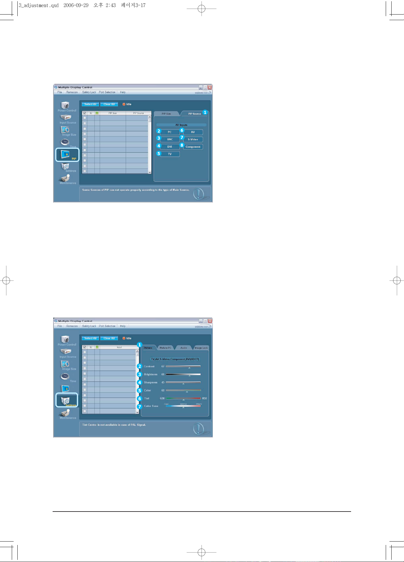
- Info grid shows some basic information necessary to PIP
Source Control.
1) PIP Source
Click the PIP Source tab to display the PIP Source list.
PIP Source can be controlled only when the power of the
monitor is turned on.
2) PC
Changes the PIP source of the selected display to PC.
3) BNC
Changes the PIP source of the selected display to BNC.
4) DVI
Changes the PIP source of the selected display to DVI.
5) TV
Changes the PIP source of the selected display to TV.
6) AV
Changes the PIP source of the selected display to AV.
7) S-Video
Changes the PIP source of the selected display to
S-Video.
8) Component
Changes the PIP source of the selected display to
Component.
Some of the PIP Sources may not be available for selection
depending on the input source type of the Main Screen.
The PIP control feature is available only for the displays whose
power status is ON and the PIP function is set to ON.
-PIP Control - PIP Source
1. Click PIP of the main icons to display the PIP control window.
- Info Grid shows some basic information necessary to
Setting Control. When each function is selected, the set
value of the selected function is displayed in the slide. As
you select Select All, the value is returned to the default
setting (50).
Changing a value in this screen will automatically change
the mode to "CUSTOM."
1) Picture
Available only for TV, AV, S-Video, Component, and
DVI(HDCP).
2) Contrast
Adjusts Contrast of the selected display.
3) Brightness
Adjusts Brightness of the selected display.
4) Sharpness
Adjusts Sharpness of the selected display.
5) Color
Adjusts Color of the selected display.
6) Tint
Adjusts Tint of the selected display.
7) Color Tone
Adjusts Color Tone of the selected display.
This feature is available only for the displays whose power status is
ON and if no selection is made, the factory default is displayed.
- Setting Control - Picture
1. Click Settings of the main icons to display the Settings Control screen.
Page 33
3. Alignment and Adjustments
3-18
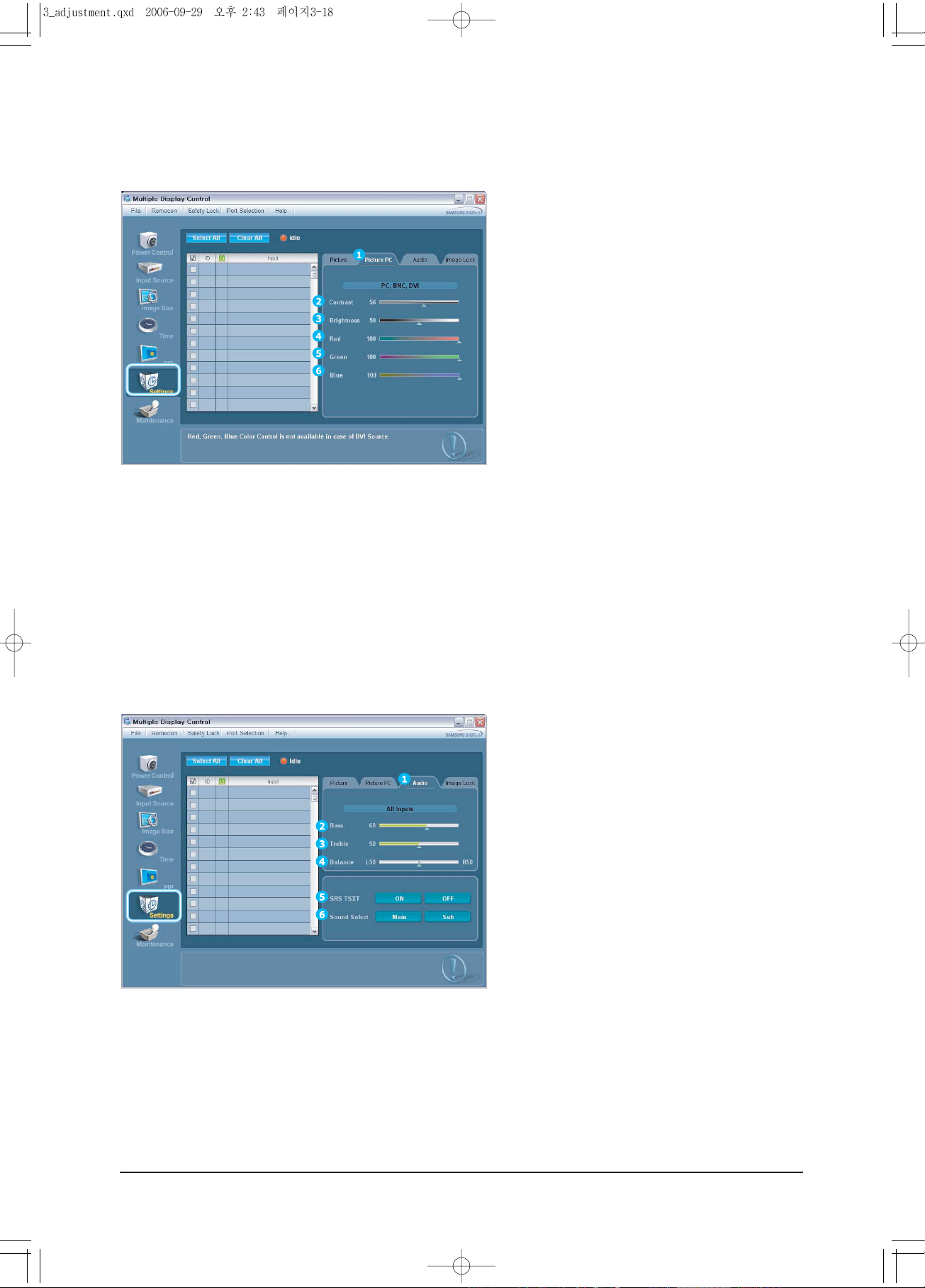
- Info Grid shows some basic information necessary to
Setting Control. When each function is selected, the set
value of the selected function is displayed in the slide. As
you select Select All, the value is returned to the default
setting (50).
Changing a value in this screen will automatically change
the mode to "CUSTOM."
1) Picture PC
Available only for PC, BNC, and DVI.
2) Contrast
Adjusts Contrast of the selected display.
3) Brightness
Adjusts Brightness of the selected display.
4) Red
Adjusts Red Color of the selected display.
5) Green
Adjusts Green Color of the selected display.
6) Blue
Adjusts Blue Color of he selected display.
This feature is available only for the displays whose power status is
ON and if no selection is made, the factory default is displayed.
-Setting Control - Picture PC
1. Click Setting of the main icons and select the Picture PC tab to display the Setting Control window.
- Info Grid shows some basic information necessary to
Setting Control. When each function is selected, the set
value of the selected function is displayed in the slide. As
you select Select All, the value is returned to the default
setting (50).
Changing a value in this screen will automatically change
the mode to "CUSTOM."
1) Audio
Controls audio setting for all input sources.
2) Bass
Adjusts Bass of the selected display.
3) Treble
Adjusts Treble of the selected display.
4) Balance
Adjusts Balance of the selected display.
5) SRS TSXT
Turns the SRS Trusurround XT function of the selected
display On/Off.
6) Sound Select
Select either Main or Sub when the PIP of the selected
display is turned On.
This feature is available only for the displays whose power status in
IN and if no selection is made, the factory default is displayed.
The MagicNet Input operates only in MagicNet models.
-Setting Control - Audio
1. Click Settings of the main icons and select the Audio tab to display the Setting Control window.
Page 34
3. Alignment and Adjustments
3-19
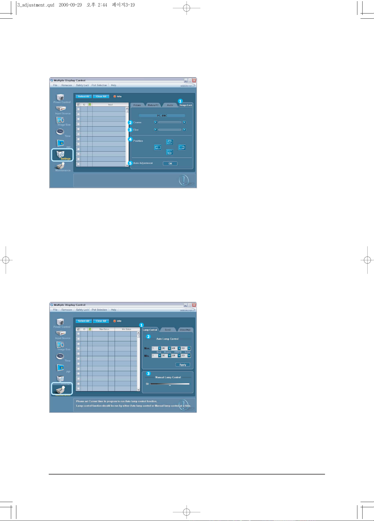
- Info Grid shows some basic information necessary to
Image Lock.
1) Image Lock
Available only the controls for PC and BNC.
2) Coarse
Adjusts Coarse of the selected display.
3) Fine
Adjusts Fine of the selected display.
4) Position
Adjusts Position of the selected display.
5) Auto Adjustment
Automatically adjusts the screen.
- This feature is available only for the displays whose
power status is ON.
-Setting Control - Image Lock
1. Click Settings of the main icons and select the Image tab to display the Setting Control window.
- Info Grid shows some basic information necessary to
Maintenance Control.
1) Lamp control
Adjusts the brightness of the lamp.
2) Auto Lamp Control
Automatically adjusts the backlight of the selected display
at a specified time. The Auto Lamp Control automatically
turns off if you adjust using the Manual Lamp Control.
3) Manual Lamp Control
Allows you to adjust the backlight of the selected display
regardless of the time.
The Manual Lamp Control automatically turns off if you
adjust using the Manual Lamp Control.
- The Maintenance Control feature is available only for the
displays whose Power Status is ON.
-Maintenance Control - Lamp Control
1. Click Maintenance of the main icons and select the Lamp Control tab to display the Maintenance Control
window.
Page 35
3. Alignment and Adjustments
3-20
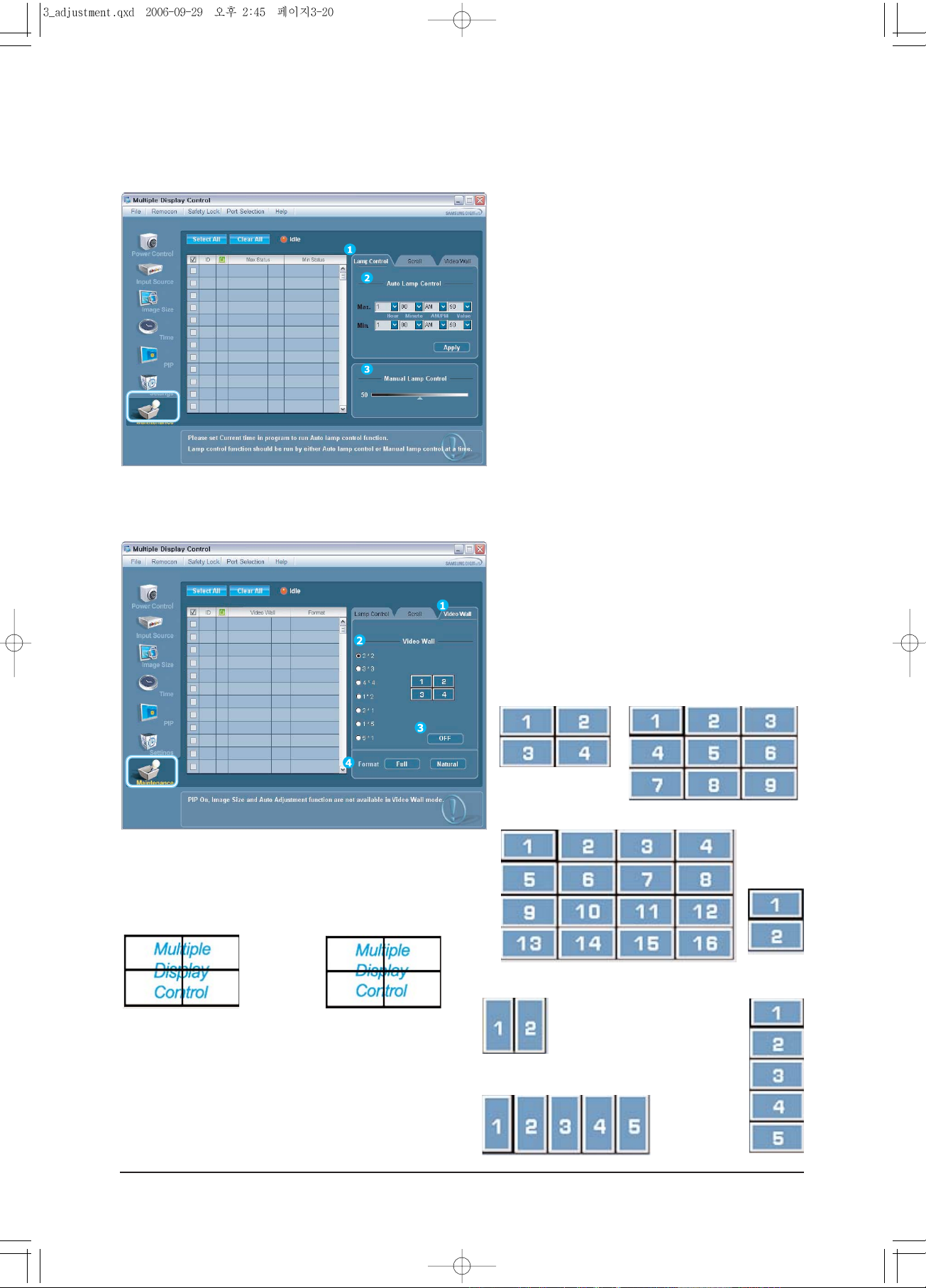
1) Screen Scroll
Eliminates the afterimages that can result when the still
image is displayed for prolonged periods. Use Interval to
set the repeat cycle by time unit and use Second to set the
repeat cycle by second unit. Select one of 4 types- Scroll,
Pixel, Bar, Eraser.
- The Maintenance Control feature is available only for the
displays whose power status in ON.
-Maintenance Control - Lamp Control
1. Click Maintenance of the main icons and select the Scroll tab to display the Maintenance Control.
1) Video Wall
A Video Wall is a set of video screens that are connected
together, so that each screen shows a part of the whole
picture or so that the same picture is repeated on each
screen.
2) Video Wall (Screen Divider)
You can select a number of screens with a different layout
when dividing.
3) On / Off
Turns On or Off the Video Wall function of the selected
display.
4) Format
The format can be selected to see a divided screen.
This feature is available only for the displays whose power
status in IN and if no selection is made, the factory default is
displayed.
The Malignant Input operates only in MagicNet models.
Full Natural
-Maintenance Control - Video Wall
1. Click Maintenance of the main icons and select the Wall tab to display the Maintenance Control window.
2 * 2 3 * 3
4 * 4
1 * 2
1 * 5
5 * 1
2 * 1
Page 36
3. Alignment and Adjustments
3-21
-Troubleshooting
1. The display you wish to control does not appear on the Power Control Info Grid
- Check the connection of RS232C. (Check if it is properly connected to the Com1 port)
- Check the displays to see if any of the other displays connected have the same ID. If more than one
displays have the same ID, those displays are not properly detected by the program due to data conflict.
- Check if the Display Set ID is a number between 1 and 10. (Adjust using the Display menu)
note : A Display Set ID must be a value between 1 and 10.
If the value is out of the range, the MDC system cannot control the display.
2. The display you wish to control does not appear on the other Control Info Grids
- Check to see if the display power is ON. (You can check this in Power Control Info Grid)
- Check if you can change the input source of the display.
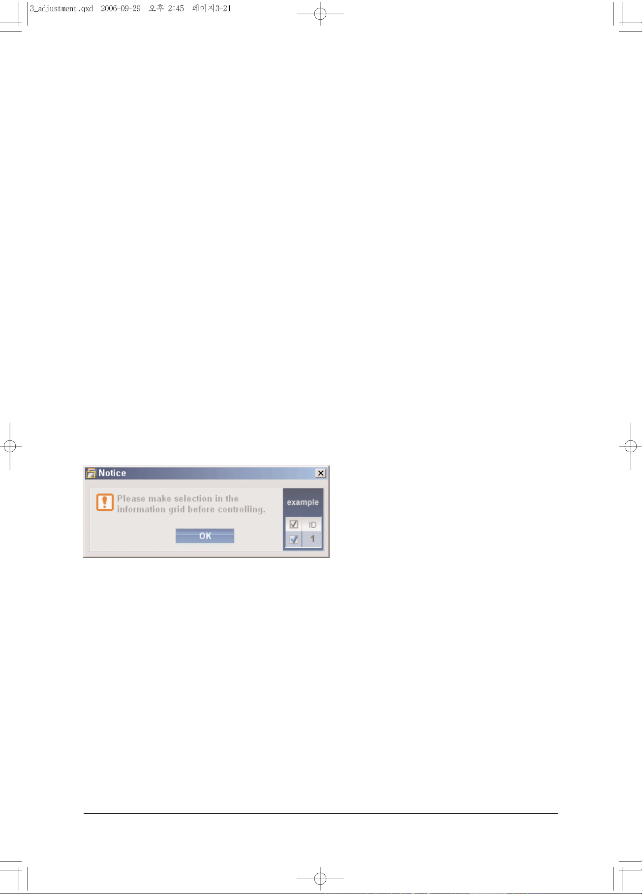
3. The dialogue box appears repeatedly.
- Check to see if the display you wish to control is selected.
4. Both On Timer and Off Timer have been set but different time is showing.
- Apply current time to synchronize the display clocks.
5. The remote may not function properly when you turn off the remote Function, disconnect the RS-232C
cable, or exit the program in an Irregular manner. Rerun the program and turn the remote function
again to Restore normal functions.
note : This program may malfunction due to problems in communication circuits or interference from electronic
appliances nearby.
Settings Value Display In Multiple Display Mode
When there are more than one displays connected, the settings values are displayed as follows.
1. No selection: Displays the Factory Default Value.
2. Selected one display: Fetches and displays the settings value for the selected display.
3. Selected one display (ID1) and add another display (ID3): The program, which was displaying the settings value of
ID 1, fetches and displays the value of ID3.
4. Selected all sets using Select All: Returns to the Factory Default Value.
Page 37
3. Alignment and Adjustments
3-22
3-7 Updating the program - MAIN
-. How to connect
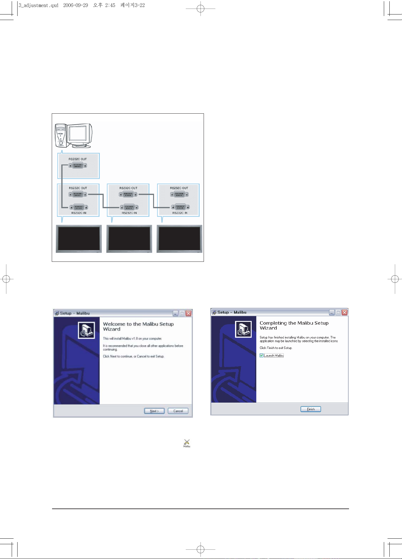
1.Connect the serial port of the PC and the input serial port of Beethoven Board with the RS232C cable.
2. Option in the Factory Menu : Check if BaudRate is set to 115200.
RS-232C, a standard of serial communication, is used for the
communication between a PC and a display. Therefore, a serial
cable should be connected between the serial port on a PC and
the serial port on a display.
Refer to the diagram.
Run the .exe file and press the ¡°OK¡± button, then press ¡°Next¡± to complete the installation. (Attached)
Malibu Flash Downloader 1.7 File
The program is not affected by Windows OS system.
When the installation is complete using the Setup.exe file , the icon appears on your desktop.
Double click the icon to run the program.
Page 38
3. Alignment and Adjustments
3-23
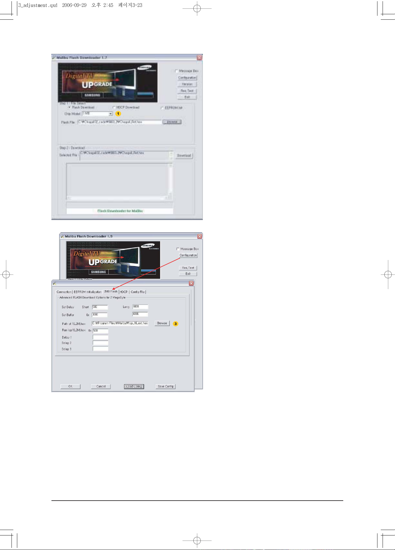
1. Flash Download in the File Select menu
Set as the figure.
Chip Model : Set 2MB_CORTEZ first.
2. After the installation
Connection
>Set as the figure
SERIAL1
COM1
115200
Page 39
3. Alignment and Adjustments
3-24
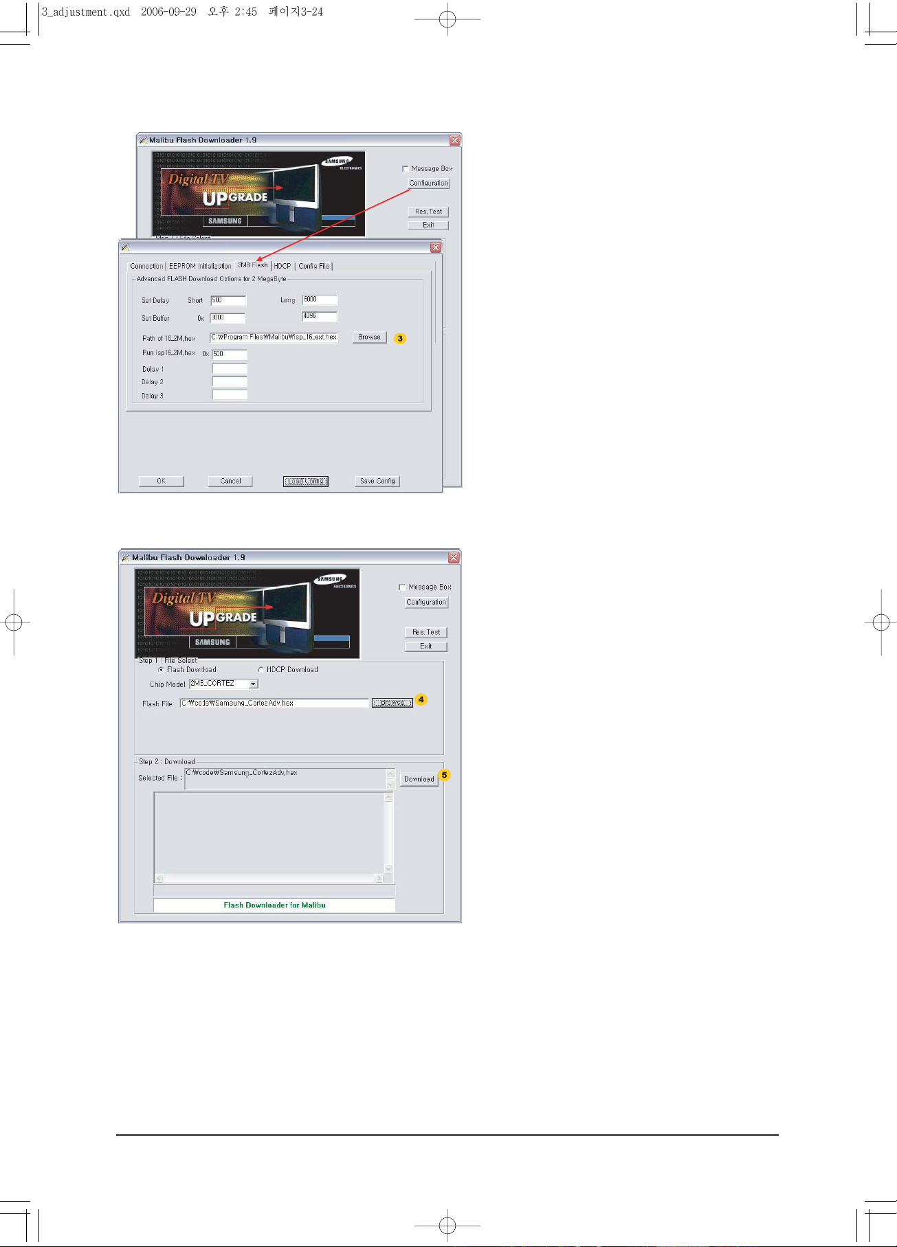
3. 2MB Flash
Isp_16_ext. Hex
Click Load Config for the auto setting.
4. Select the file you want to download on Browse.
5. Press 5 to download.
Turn the power of the board off/on when the download
success message appears.
Check the Checksum and date to see if the right code is
applied in the Factory mode.
Page 40
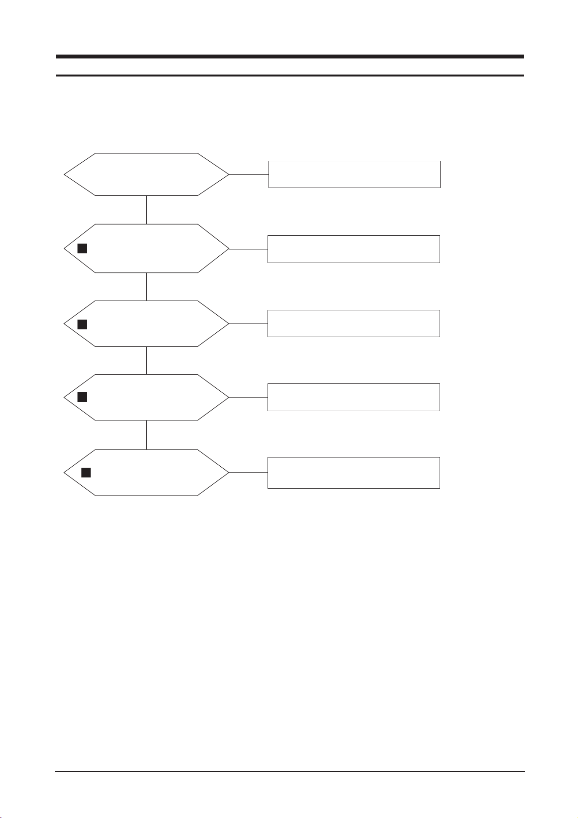
4 Troubleshooting
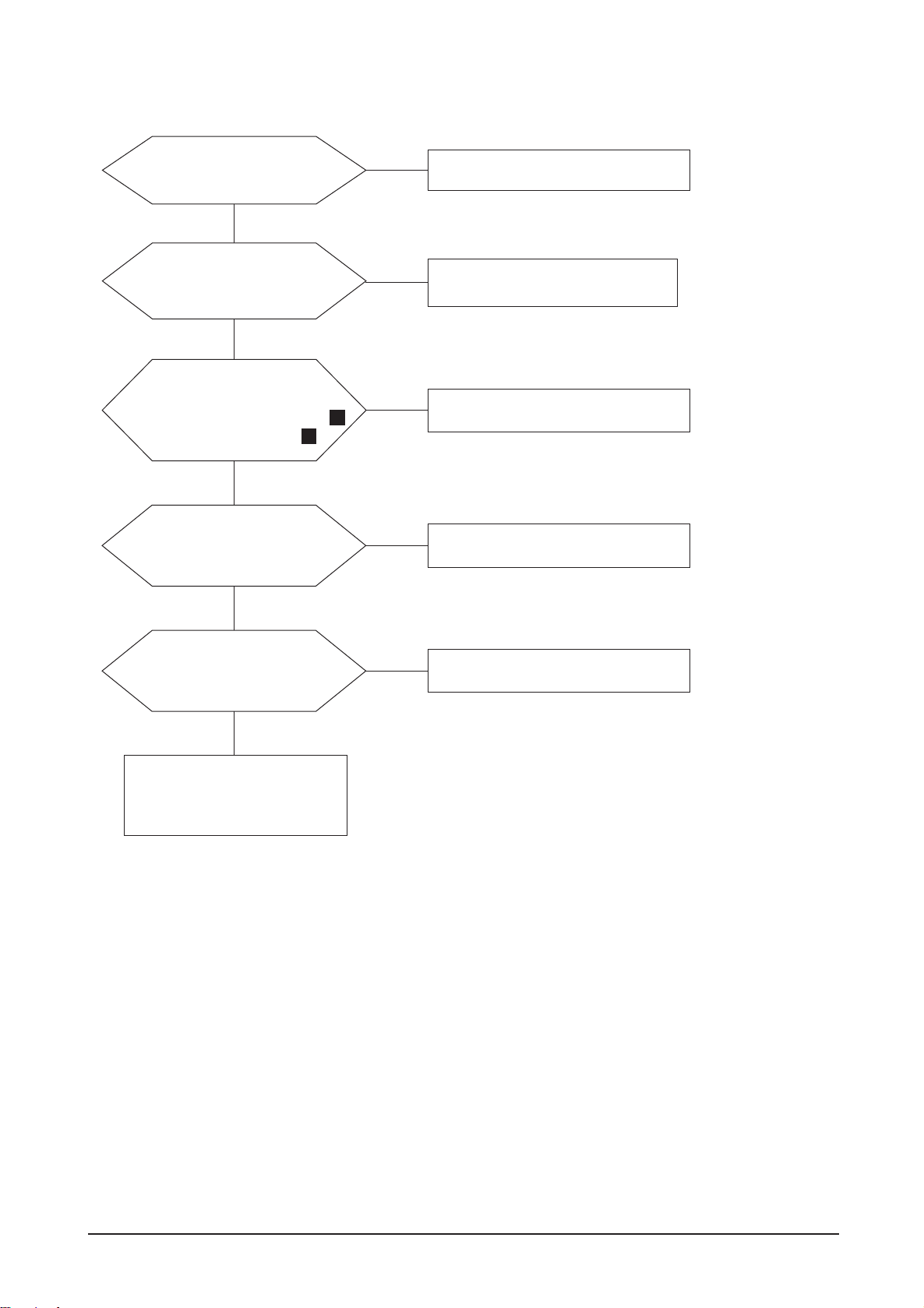
4-1 No Power
4 Troubleshooting
Does 12 V appear at
Pin 12V of CN602?
YES
Does DC 12V appear at
1
Does 3.3V appear at
2
Does DC 1.8V appear at
3
C653?
YES
C622?
YES
C603?
YES
NO
Check the IP Board.
NO
Check the peripheral circuit of CN602.
NO
Replace IC602.
NO
Replace IC601.
Does 3.3 V appear at Pin
4
16 ofCN602?
NO
The Scaler(IC408) is abnormal.
Replace the main board.
4-1
Page 41
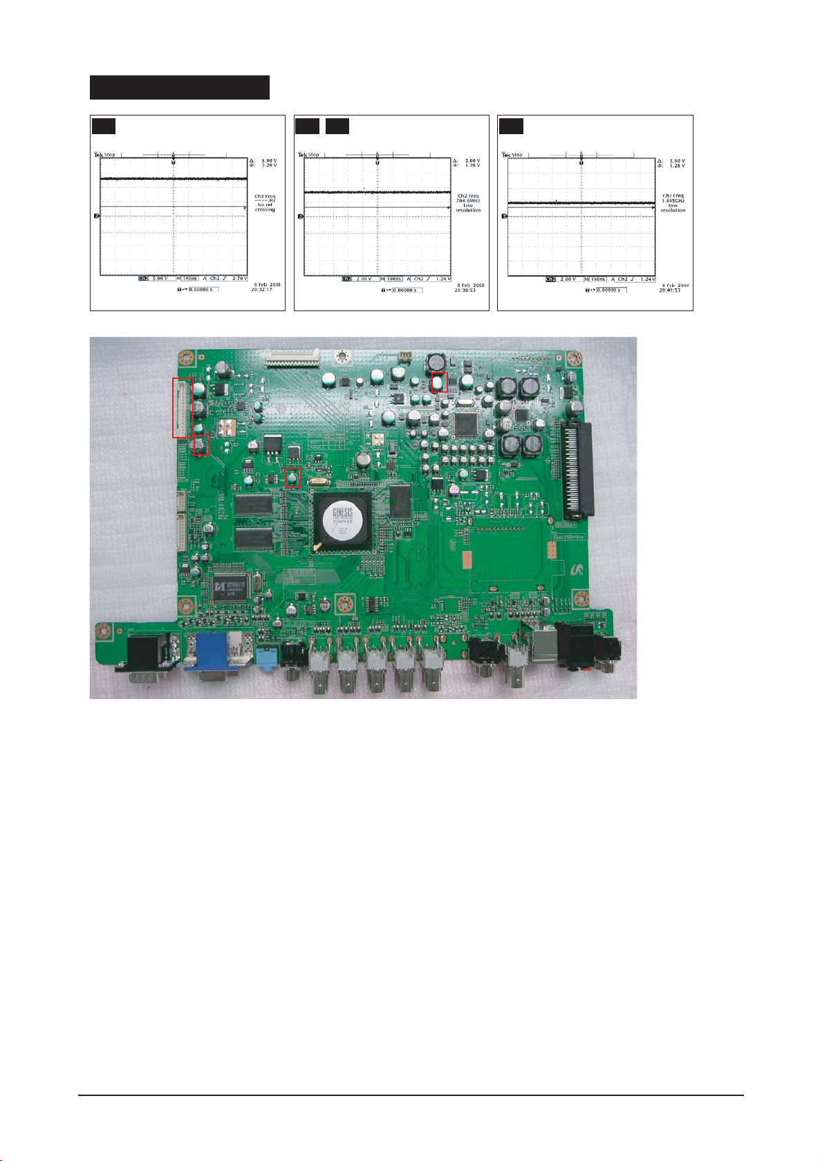
4 Troubleshooting
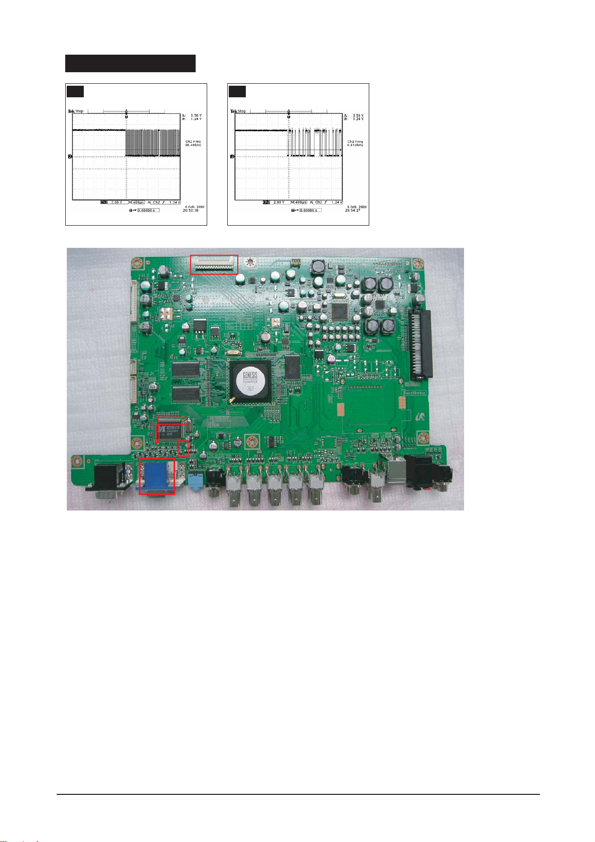
WAVEFORMS
1
2 4 3
CN602
C622
C603
C653
4-2
Page 42
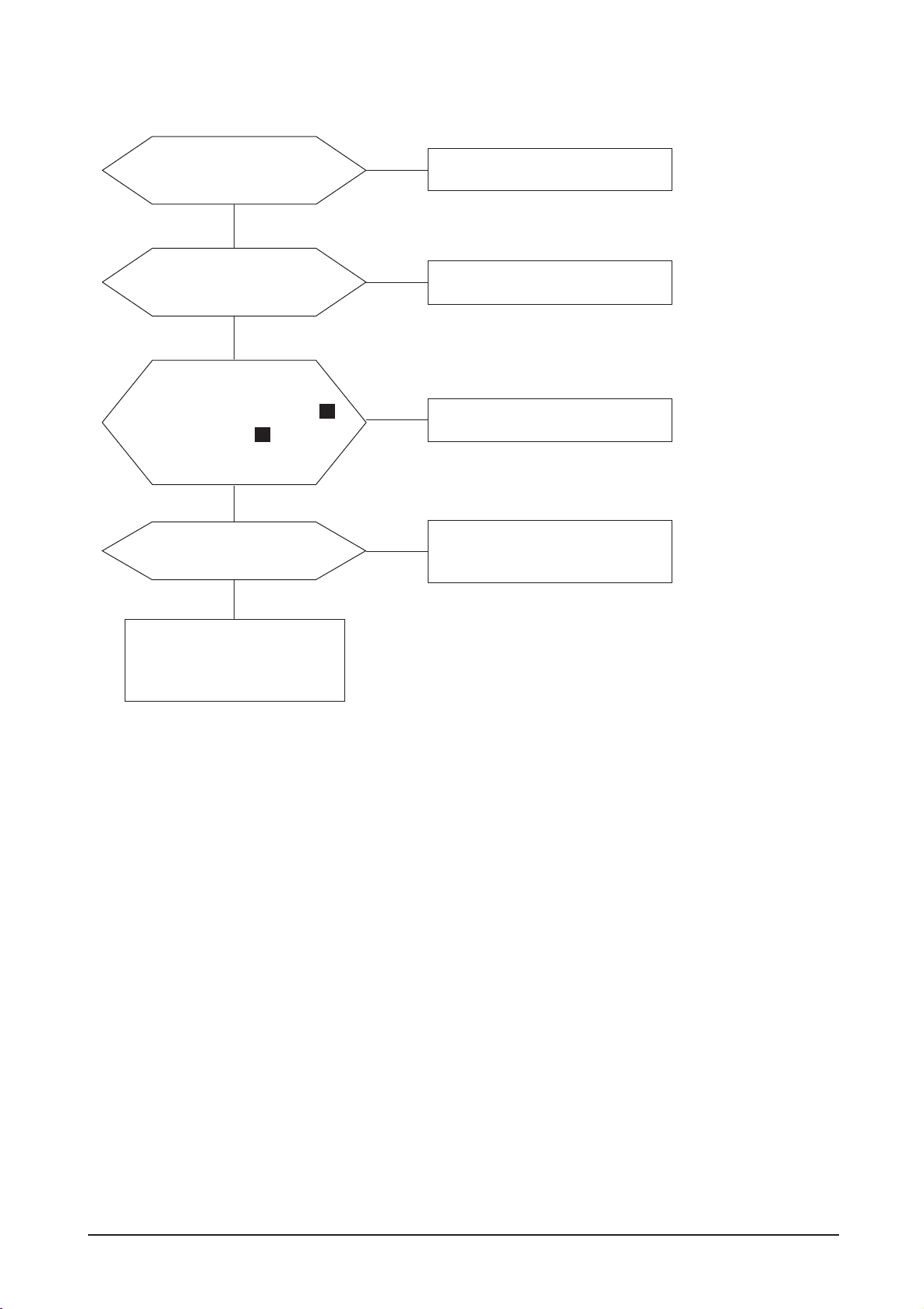
4-2 No PC(D-SUB) Video
4 Troubleshooting
Does the LED light up when
turn on the power?
YES
Does 5V appear at Pin 9 of
CN101 D-Sub?
YES
Does the waveform as the
figure at Pin 6 ( H-sync)
and Pin 8 (V-sync) of IC103
6
5
appear?
YES
Is TX** signal sent to Pin 14
and 15 of CN403 14, 15?
YES
NO
NO
NO
NO
Check the power port.
Check the cable connection.
Replace IC103.
The Scaler(IC408) is abnormal.
Replace the main board.
Check the cable between the
main board and panel and
replace the LCD panel.
4-3
Page 43
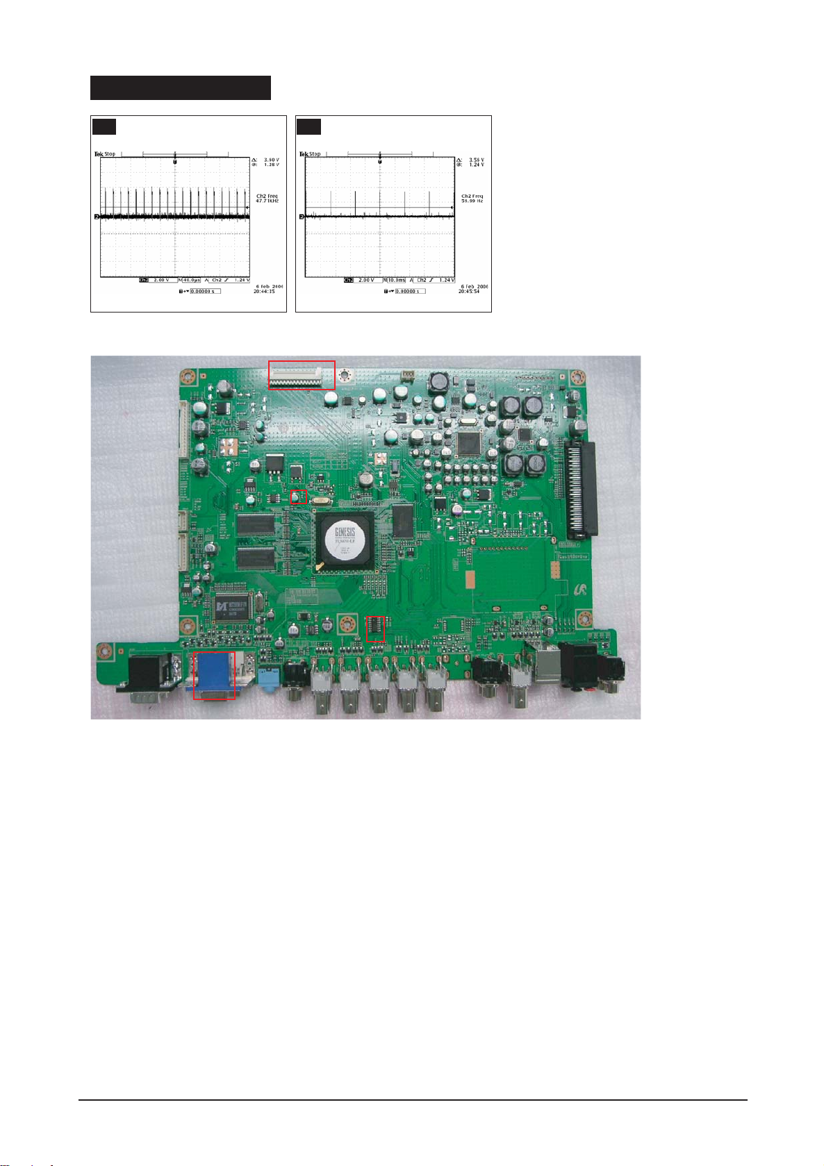
4 Troubleshooting
WAVEFORMS
5
5
66
CN403
CN101
C603
IC103
4-4
Page 44
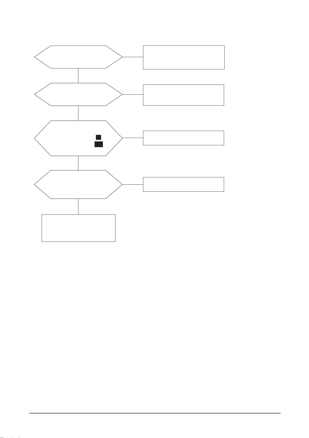
4-3 No DVI Video
4 Troubleshooting
Does the LED light up when
turn on the power?
YES
Does 5 V appear at Pin 14 and
16 of CN101 DVI port?
YES
Does the wave form as the figure
appear at R161(DVI_SCL)
and R162(DVI_SDA) ?
7
8
YES
Does the signal appear at
RA107(R), RA102(G), and
RA105(B)?
NO
NO
NO
NO
Check the power port.
Check the cable connection.
Replace the main board.
IC105 is abnormal. Replace the
main board.
YES
Does the TX** signal appear at
Pin 14 and 15 of CN403?
YES
Check the cable between the
main board and panel
and replace the LCD panel.
NO
The Scaler (IC408) is abnormal.
Replace the main board.
4-5
Page 45
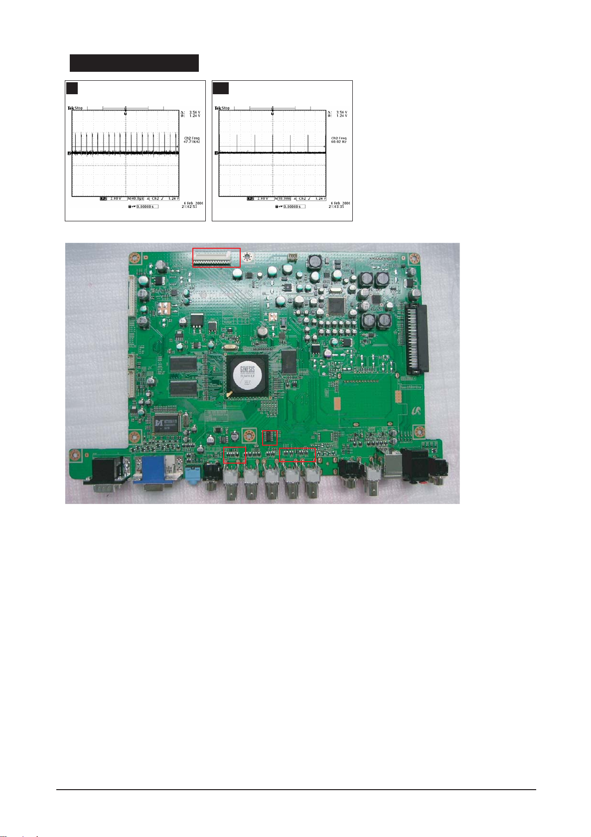
4 Troubleshooting
WAVEFORMS
7 8
CN403
CN101
RA102, 105, 107
R161
R162
4-6
Page 46
4-4 No BNC Video
4 Troubleshooting
Does 3.3 V appear at
ZD109 ~ 113?
YES
Is the cable properly
connected?
YES
Does the wave form appear at
Pin 6 (H-sync)
And Pin 8 (V-sync) of
9
10
IC103?
YES
Does the TX** signal appear
at Pin 14 and 15
of CN403?
NO
NO
NO
NO
Press the power button and
check the LED.
Reconnect the BNC cable.
Replace IC103.
The scaler (IC408) is abnormal.
Replace the main board.
YES
Check the cable between the
main board and panel and
replace the LCD panel.
4-7
Page 47
4 Troubleshooting
WAVEFORMS
9 10
CN403
ZD109
IC103
ZD110~113
4-8
5-6
Page 48
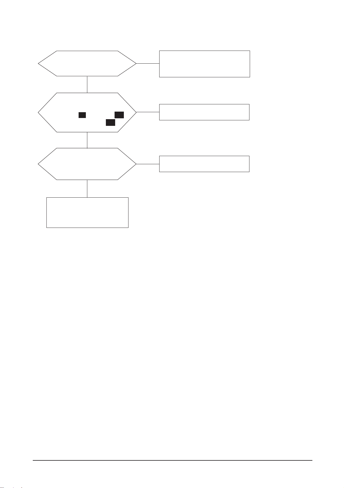
4-5 No Component Video
4 Troubleshooting
Does 3.3V appear at
ZD109 ~ 113?
YES
Does the waceform appear at
R1011(Pr) ,R1012(Y) ,
11
R1013 (Pb)?
12
13
YES
Does the TX** signal appear
at Pin 14 and 15
of CN403?
YES
Check the cable between the
main board and panel and
replace the LCD panel.
NO
NO
NO
Press the power button and
check the LED.
Reconnect the component cable.
The scaler (IC408) is abnormal.
Replace the main board.
4-9
Page 49
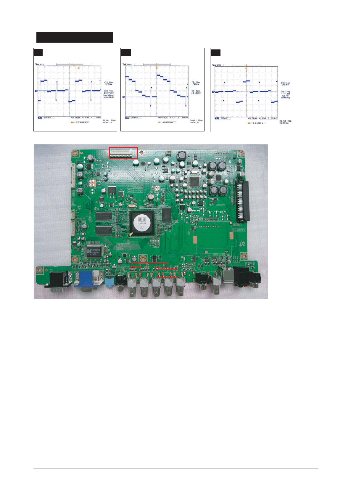
4 Troubleshooting
WAVEFORMS
11 12
CN403
13
ZD109
R1011~R1013
ZD110~113
4-10
Page 50
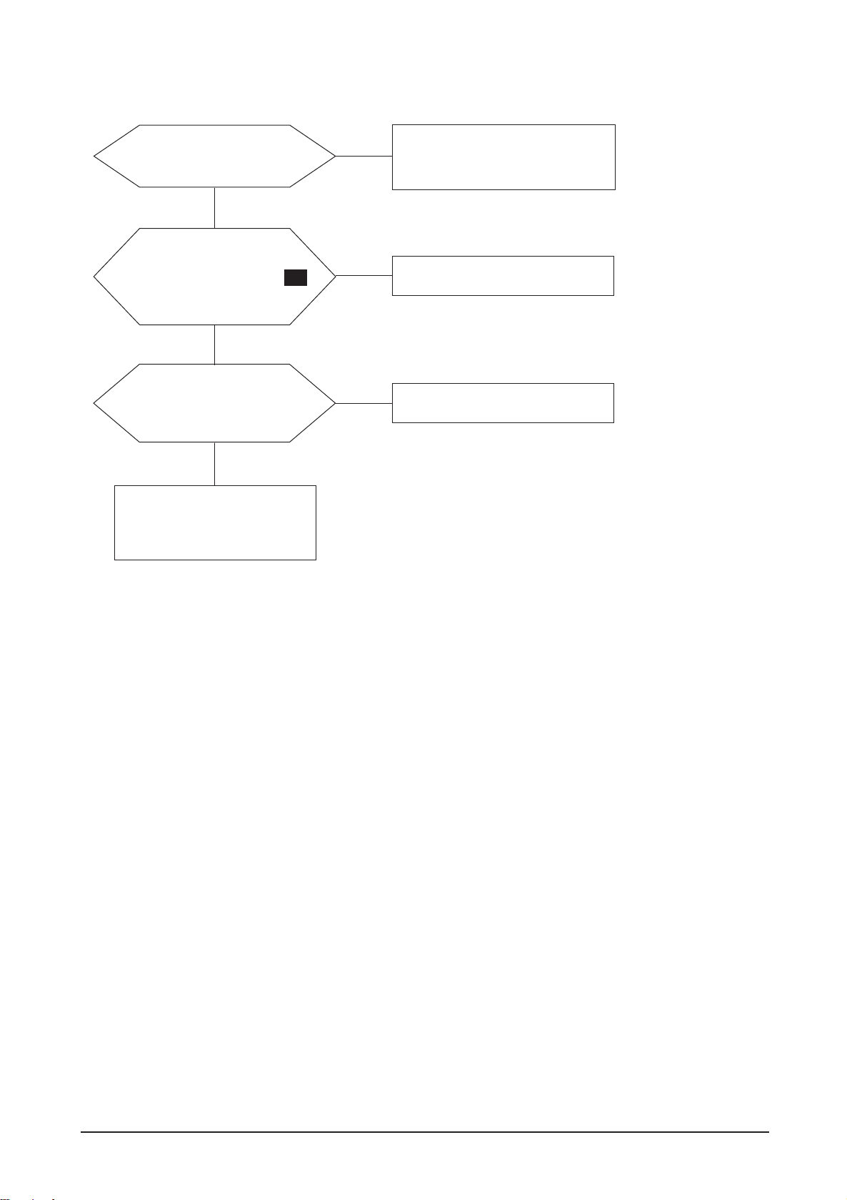
4-6 No Component Video
4 Troubleshooting
Does the LED light up when
turn on the power?
YES
Does the waveform at L101 ?
YES
Does the TX** signal appear
at Pin 14 and 15
of CN403?
YES
Check the cable between the
main board and panel and
replace the LCD panel.
14
NO
NO
NO
Check the power port.
Reconnect the cable.
The scaler (IC408) is abnormal.
Replace the main board.
4-11
Page 51
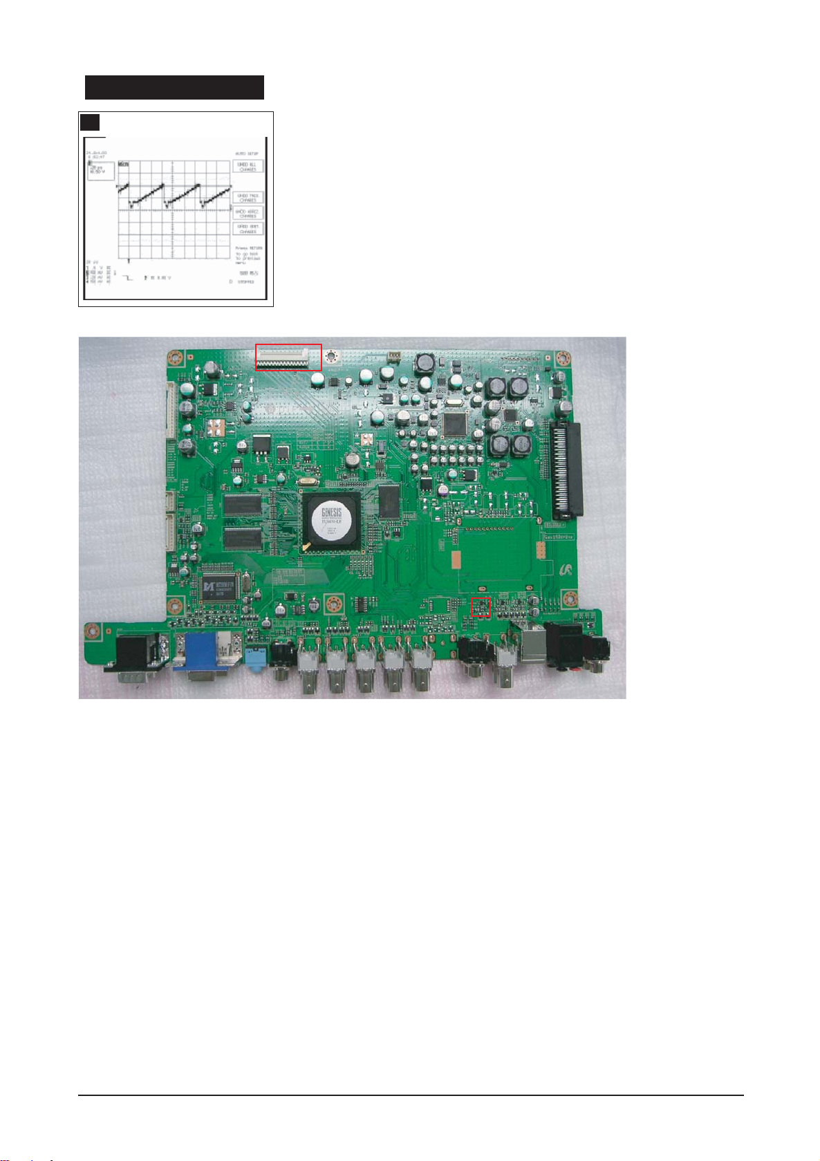
4 Troubleshooting
WAVEFORMS
14
CN403
L101
4-12
Page 52
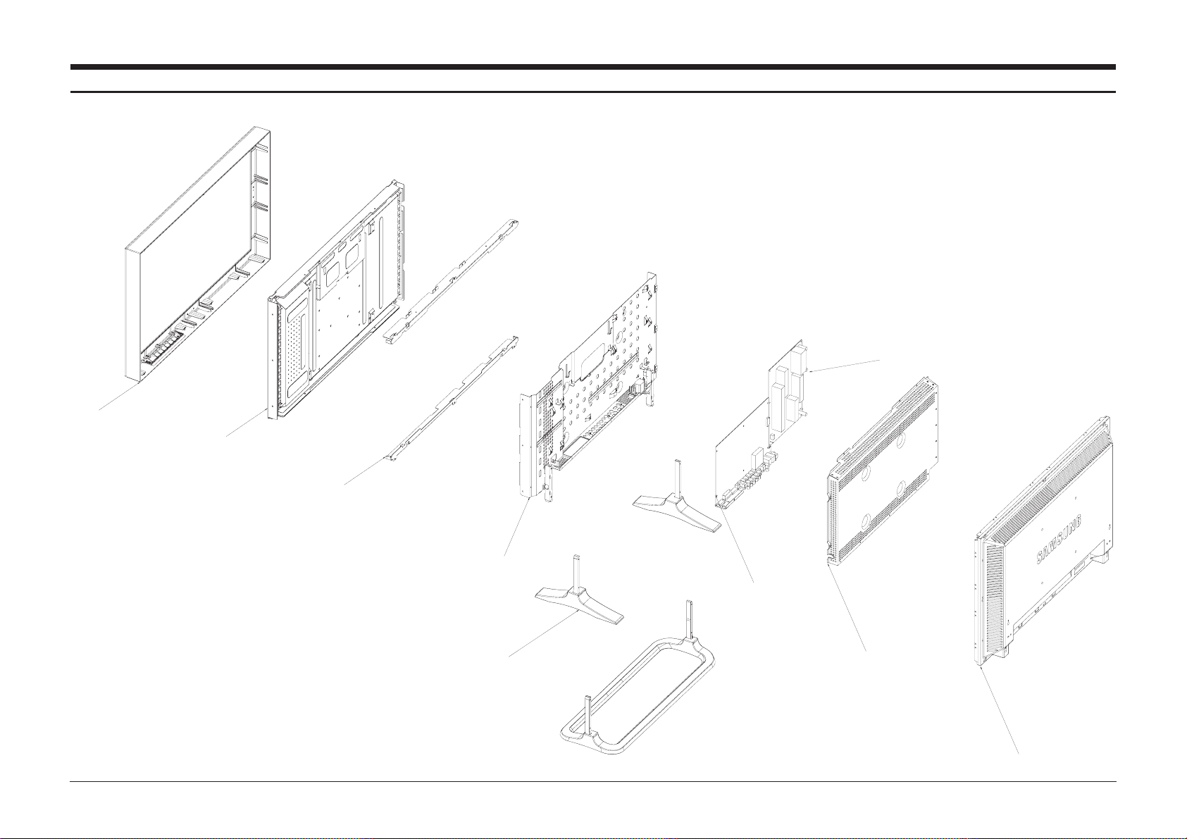
5 Exploded View & Parts List
5-1
5 Exploded View & Parts List
5-1 Exploded View
T0003
M0215
T0764
M0146
M0412
M0003
M0014
T0178
M0013
Page 53
5 Exploded View & Parts List
5-2
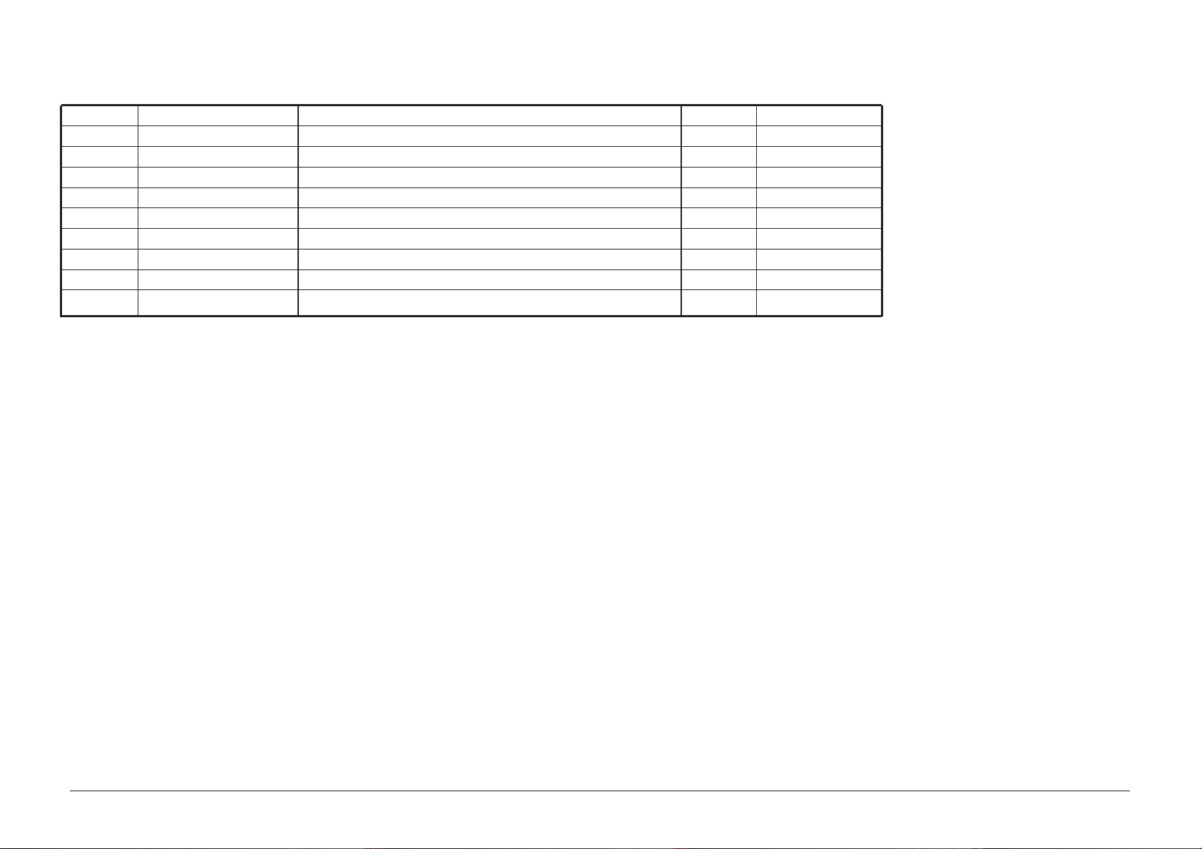
5-2 Parts List
Location.No
CODE-NO SPECIFICATION & DESCRIPTION Q'TY S.A/SNA
T0003 BN96-02512K ASSY COVER P-FRONT;LS32BH (S/M 320PX),HI 1 S.A
M0215 BN07-00368A LCD-PANEL;LTA320WT-L16,LTA320WT-L16,8bit 1 S.A
M0146 BN61-01993A BRACKET-PANEL TOP;BE32PS,SECC,T1.2 2 S.N.A
M0412 BN96-02514E ASSY BRACKET P-PCB;BEETHOVEN,SECC,1.0,BE 1 S.N.A
T0764 BN44-00153A SMPS-LCD MONITOR;MGM32MT,DYREL,AC/DC,180 1 S.A
M0014 BN94-00744K ASSY PCB MAIN-SPZ;LS32BHPNS/EDC,W/W,AMLC 1 S.A
T0178 BN63-02123B SHIELD-PCB;BEETHOVEN,SECC,1.0,BEETHOVEN3 1 S.N.A
M0013 BN96-02513C ASSY COVER P-REAR;LS32BH,ABS V0 GR37 1 S.A
M0003 BN96-00452E ASSY STAND P;BE46PS,AL DIECASTING,BKN-S2 1 S.A
Page 54
6 Electrical Parts List
-You can search for updated part codes through ITSELF web site.
URL : http://itself.sec.samsung.co.kr/
6-1 Parts List
6 Electrical Parts List
6-1
Level Loc. No. Code No. Description & Specification Q'ty SA/SNA
LS32BHPNB/XSF 320PX,WXP1/S32P1-LBH,32,LCD-MO,CHINA
0.1 M0001 BN90-01107C ASSY COVER FRONT;LS32BHPNB/XSF 1 S.N.A
..2 T0003 BN96-02512K ASSY COVER P-FRONT;LS32BH (S/M 320PX),HI 1 S.A
...3 M0081 6003-000282 SCREW-TAPTITE;BH,+,-,B,M3,L8,ZPC(BLK),SW 4 S.N.A
...3 T0081 BN61-00408A GUIDE-FUNCTION;CK40PS,ABS,GR503,HB 1 S.N.A
...3 M0112 BN63-02115B COVER-FRONT;BE32PS,HIPS,T3.2,HB,BK502 1 S.N.A
...3 M0007 BN64-00156D KNOB-FUNCTION;BE46PS,ABS,HB,BK07 1 S.N.A
...3 T0299 BN64-00352A WINDOW-RMC LED;BEETHOVEN 46,PC,ACRAY,BKM 1 S.N.A
...3 M0020 BN96-03565A ASSY BOARD P;BEETHOVEN 2,FUNCTION & IR 1 S.A
...3 AA64-04418A LOGO-BADGE;Z50,AL,1.2,2g,65mm,SILVER,SAM 1 S.N.A
..2 T0382 BP61-00495C HOLDER-CARE;PJT,ACRYL-FOAM,T0.25,W30.0mm 0.2 S.N.A
0.1 M0002 BN90-01108A ASSY COVER REAR;LS32BHPNS/EDC 1 S.N.A
..2 M0081 6003-001026 SCREW-TAPTITE;RH,+,B,M4,L15,ZPC(BLK),SWR 6 S.A
..2 M0013 BN96-02513C ASSY COVER P-REAR;LS32BH,ABS V0 GR37 1 S.A
...3 M0081 6003-001321 SCREW-TAPTITE;BH,+,B,M4,L8,ZPC(BLK),SWRC 4 S.A
...3 BN61-00076B GUIDE-HOOK;LS32BEP,STS,T2.0,BKN-S204 2 S.N.A
...3 M0113 BN61-01505B BRACKET-VESA;LS32BEP,SECC,1.6 1 S.N.A
...3 T0578 BN64-00405B INLAY AV;BEETHOVEN32",PS,0.5,LS32BH 1 S.N.A
...3 M0006 BN63-02117B COVER-REAR;BEETHOVEN,ABS,3.0,V0,GR37,BEE 1 S.N.A
0.1 M0017 BN91-01013P ASSY CHASSIS-SPZ;LS32BHPNS/EDC 1 S.N.A
..2 M0014 BN94-00744K ASSY PCB MAIN-SPZ;LS32BHPNS/EDC,W/W,AMLC 1 S.A
...3 T0245 0202-001492 SOLDER-WIRE FLUX;HSE-02 LFM48 SR-34 S,-, 0.25 S.N.A
...3 CN109 3701-001312 CONNECTOR-DSUB;9P/2C,2R,MALE,ANGLE,AUF 1 S.A
...3 CN101 3701-001334 CONNECTOR-DVI;24P(DVI)+15P(D-SUB),6,FEMA 1 S.A
...3 CN906 3705-001360 CONNECTOR-COAXIAL;BNC,FEMALE,-,75ohm,- 1 S.A
...3 CN906 3705-001360 CONNECTOR-COAXIAL;BNC,FEMALE,-,75ohm,- 1 S.A
...3 CN906 3705-001360 CONNECTOR-COAXIAL;BNC,FEMALE,-,75ohm,- 1 S.A
...3 CN906 3705-001360 CONNECTOR-COAXIAL;BNC,FEMALE,-,75ohm,- 1 S.A
...3 CN906 3705-001360 CONNECTOR-COAXIAL;BNC,FEMALE,-,75ohm,- 1 S.A
...3 CN906 3705-001360 CONNECTOR-COAXIAL;BNC,FEMALE,-,75ohm,- 1 S.A
...3 CN906 3711-004182 CONNECTOR-HEADER;BOX,10P,1R,2MM,STRAIGHT 1 S.A
...3 CN330 3711-004349 HEADER-BOARD TO CABLE;BOX,3P,1R,2mm,STRA 1 S.A
...3 CN330 3711-004484 HEADER-BOARD TO CABLE;BOX,5P,1R,2mm,STRA 1 S.A
...3 CN403 3711-005884 HEADER-BOARD TO BOARD;BOX,30P,2R,2mm,ANG 1 S.A
...3 CN330 3711-005942 HEADER-BOARD TO CABLE;BOX,16P,1R,2mm,STR 1 S.A
...3 CN110 3722-002000 JACK-DIN;4P/2C,NI,BLK,ANGLE 1 S.A
...3 CN502 3722-002081 JACK-EAR PHONE;5P/2C,-,SnPb,L-BLU,- 1 S.A
...3 JA333 3722-002285 JACK-PIN;2P,NI,WHT/RED,ANGLE 1 S.A
...3 JA333 3722-002285 JACK-PIN;2P,NI,WHT/RED,ANGLE 1 S.A
...3 JA333 3722-002285 JACK-PIN;2P,NI,WHT/RED,ANGLE 1 S.A
...3 T0562 6046-001014 STAND OFF;#4-40,L6,NI PLT,C3601,- 8 S.N.A
...3 CN506 BN37-00004A CONN TERMINAL;PST038-01,BE32PXn,27.5 mm, 1 S.A
...3 CIS BN63-01710B SHIELD-JACK;BE46PS,SPTE,0.5,CHANGE CORE 1 S.N.A
...3 T0174 BN97-00894H ASSY SMD;LS32BHPNS/EDC,W/W 1 S.N.A
....4 SUB05 0202-001477 SOLDER-CREAM;LST309-M,-,D20~45§-,96.5Sn/ 3.663 S.N.A
....4 D101 0401-001056 DIODE-SWITCHING;MMBD4148SE,100V,200mA,SO 1 S.A
....4 D102 0401-001056 DIODE-SWITCHING;MMBD4148SE,100V,200mA,SO 1 S.A
....4 D103 0401-001056 DIODE-SWITCHING;MMBD4148SE,100V,200mA,SO 1 S.A
....4 D104 0401-001056 DIODE-SWITCHING;MMBD4148SE,100V,200mA,SO 1 S.A
....4 D105 0401-001056 DIODE-SWITCHING;MMBD4148SE,100V,200mA,SO 1 S.A
Page 55
6 Electrical Parts List
6-2
Level Loc. No. Code No. Description & Specification Q'ty SA/SNA
....4 D106 0401-001056 DIODE-SWITCHING;MMBD4148SE,100V,200mA,SO 1 S.A
....4 D107 0401-001056 DIODE-SWITCHING;MMBD4148SE,100V,200mA,SO 1 S.A
....4 D108 0401-001056 DIODE-SWITCHING;MMBD4148SE,100V,200mA,SO 1 S.A
....4 D109 0401-001056 DIODE-SWITCHING;MMBD4148SE,100V,200mA,SO 1 S.A
....4 D110 0401-001056 DIODE-SWITCHING;MMBD4148SE,100V,200mA,SO 1 S.A
....4 D111 0401-001056 DIODE-SWITCHING;MMBD4148SE,100V,200mA,SO 1 S.A
....4 D113 0401-001056 DIODE-SWITCHING;MMBD4148SE,100V,200mA,SO 1 S.A
....4 D114 0401-001056 DIODE-SWITCHING;MMBD4148SE,100V,200mA,SO 1 S.A
....4 D115 0401-001056 DIODE-SWITCHING;MMBD4148SE,100V,200mA,SO 1 S.A
....4 D116 0401-001056 DIODE-SWITCHING;MMBD4148SE,100V,200mA,SO 1 S.A
....4 D117 0401-001056 DIODE-SWITCHING;MMBD4148SE,100V,200mA,SO 1 S.A
....4 D118 0401-001056 DIODE-SWITCHING;MMBD4148SE,100V,200mA,SO 1 S.A
....4 D119 0401-001056 DIODE-SWITCHING;MMBD4148SE,100V,200mA,SO 1 S.A
....4 D120 0401-001056 DIODE-SWITCHING;MMBD4148SE,100V,200mA,SO 1 S.A
....4 D122 0401-001056 DIODE-SWITCHING;MMBD4148SE,100V,200mA,SO 1 S.A
....4 D123 0401-001056 DIODE-SWITCHING;MMBD4148SE,100V,200mA,SO 1 S.A
....4 D124 0401-001056 DIODE-SWITCHING;MMBD4148SE,100V,200mA,SO 1 S.A
....4 D125 0401-001056 DIODE-SWITCHING;MMBD4148SE,100V,200mA,SO 1 S.A
....4 D126 0401-001056 DIODE-SWITCHING;MMBD4148SE,100V,200mA,SO 1 S.A
....4 D127 0401-001056 DIODE-SWITCHING;MMBD4148SE,100V,200mA,SO 1 S.A
....4 D128 0401-001056 DIODE-SWITCHING;MMBD4148SE,100V,200mA,SO 1 S.A
....4 D129 0401-001056 DIODE-SWITCHING;MMBD4148SE,100V,200mA,SO 1 S.A
....4 D130 0401-001056 DIODE-SWITCHING;MMBD4148SE,100V,200mA,SO 1 S.A
....4 D131 0401-001056 DIODE-SWITCHING;MMBD4148SE,100V,200mA,SO 1 S.A
....4 D132 0401-001056 DIODE-SWITCHING;MMBD4148SE,100V,200mA,SO 1 S.A
....4 D133 0401-001056 DIODE-SWITCHING;MMBD4148SE,100V,200mA,SO 1 S.A
....4 D140 0401-001099 DIODE-SWITCHING;1N4148WS,75V,150mA,SOD-3 1 S.A
....4 D141 0401-001099 DIODE-SWITCHING;1N4148WS,75V,150mA,SOD-3 1 S.A
....4 D142 0401-001099 DIODE-SWITCHING;1N4148WS,75V,150mA,SOD-3 1 S.A
....4 D143 0401-001099 DIODE-SWITCHING;1N4148WS,75V,150mA,SOD-3 1 S.A
....4 D144 0401-001099 DIODE-SWITCHING;1N4148WS,75V,150mA,SOD-3 1 S.A
....4 D145 0401-001099 DIODE-SWITCHING;1N4148WS,75V,150mA,SOD-3 1 S.A
....4 D146 0401-001099 DIODE-SWITCHING;1N4148WS,75V,150mA,SOD-3 1 S.A
....4 D147 0401-001099 DIODE-SWITCHING;1N4148WS,75V,150mA,SOD-3 1 S.A
....4 D112 0402-000553 DIODE-SCHOTTKY;SS24/B240,40V,2000mA,DO-2 1 S.A
....4 D603 0402-000553 DIODE-SCHOTTKY;SS24/B240,40V,2000mA,DO-2 1 S.A
....4 ZD601 0402-000553 DIODE-SCHOTTKY;SS24/B240,40V,2000mA,DO-2 1 S.A
....4 ZD602 0402-000553 DIODE-SCHOTTKY;SS24/B240,40V,2000mA,DO-2 1 S.A
....4 D516 0402-001614 DIODE-RECTIFIER;S1G,400V,1A,DO-214AC,TP 1 S.A
....4 D513 0403-000258 DIODE-ZENER;BZX84C5V6,5.2-6V,225mW,SOT-2 1 S.A
....4 D514 0403-000258 DIODE-ZENER;BZX84C5V6,5.2-6V,225mW,SOT-2 1 S.A
....4 ZD403 0403-000277 DIODE-ZENER;MMBZ5226B,3.14-3.47V,225MW,S 1 S.A
....4 ZD404 0403-000277 DIODE-ZENER;MMBZ5226B,3.14-3.47V,225MW,S 1 S.A
....4 ZD101 0403-000579 DIODE-ZENER;BZX84C5V1,4.8-5.4V,200mW,SOT 1 S.A
....4 ZD103 0403-000579 DIODE-ZENER;BZX84C5V1,4.8-5.4V,200mW,SOT 1 S.A
....4 ZD104 0403-000579 DIODE-ZENER;BZX84C5V1,4.8-5.4V,200mW,SOT 1 S.A
....4 ZD105 0403-000579 DIODE-ZENER;BZX84C5V1,4.8-5.4V,200mW,SOT 1 S.A
....4 ZD107 0403-000579 DIODE-ZENER;BZX84C5V1,4.8-5.4V,200mW,SOT 1 S.A
....4 ZD108 0403-000579 DIODE-ZENER;BZX84C5V1,4.8-5.4V,200mW,SOT 1 S.A
....4 ZD109 0403-000579 DIODE-ZENER;BZX84C5V1,4.8-5.4V,200mW,SOT 1 S.A
....4 ZD119 0403-000579 DIODE-ZENER;BZX84C5V1,4.8-5.4V,200mW,SOT 1 S.A
....4 ZD124 0403-000579 DIODE-ZENER;BZX84C5V1,4.8-5.4V,200mW,SOT 1 S.A
....4 ZD110 0403-001052 DIODE-ZENER;RD8.2MB,7.7-8.7V,200mW,SOT-2 1 S.A
....4 ZD111 0403-001052 DIODE-ZENER;RD8.2MB,7.7-8.7V,200mW,SOT-2 1 S.A
....4 ZD112 0403-001052 DIODE-ZENER;RD8.2MB,7.7-8.7V,200mW,SOT-2 1 S.A
....4 ZD113 0403-001052 DIODE-ZENER;RD8.2MB,7.7-8.7V,200mW,SOT-2 1 S.A
....4 ZD115 0403-001052 DIODE-ZENER;RD8.2MB,7.7-8.7V,200mW,SOT-2 1 S.A
....4 ZD116 0403-001052 DIODE-ZENER;RD8.2MB,7.7-8.7V,200mW,SOT-2 1 S.A
....4 ZD117 0403-001052 DIODE-ZENER;RD8.2MB,7.7-8.7V,200mW,SOT-2 1 S.A
....4 ZD118 0403-001052 DIODE-ZENER;RD8.2MB,7.7-8.7V,200mW,SOT-2 1 S.A
Page 56
....4 ZD120 0403-001052 DIODE-ZENER;RD8.2MB,7.7-8.7V,200mW,SOT-2 1 S.A
....4 ZD121 0403-001052 DIODE-ZENER;RD8.2MB,7.7-8.7V,200mW,SOT-2 1 S.A
....4 ZD122 0403-001052 DIODE-ZENER;RD8.2MB,7.7-8.7V,200mW,SOT-2 1 S.A
....4 ZD123 0403-001052 DIODE-ZENER;RD8.2MB,7.7-8.7V,200mW,SOT-2 1 S.A
....4 ZD102 0403-001435 DIODE-ZENER;QZX363C5V6,5.32-5.88V,200MW, 1 S.A
....4 ZD106 0403-001435 DIODE-ZENER;QZX363C5V6,5.32-5.88V,200MW, 1 S.A
....4 ZD401 0403-001435 DIODE-ZENER;QZX363C5V6,5.32-5.88V,200MW, 1 S.A
....4 ZD402 0403-001435 DIODE-ZENER;QZX363C5V6,5.32-5.88V,200MW, 1 S.A
....4 D6020 0404-001271 DIODE-SCHOTTKY;SSA34,40V,3000mA,SMA,TP 1 S.A
....4 D501 0406-001163 DIODE-TVS;CDS3C05GTA,6.4V/-/-,-,SMD 1 S.A
....4 D502 0406-001163 DIODE-TVS;CDS3C05GTA,6.4V/-/-,-,SMD 1 S.A
....4 D503 0406-001163 DIODE-TVS;CDS3C05GTA,6.4V/-/-,-,SMD 1 S.A
....4 D504 0406-001163 DIODE-TVS;CDS3C05GTA,6.4V/-/-,-,SMD 1 S.A
....4 D505 0406-001163 DIODE-TVS;CDS3C05GTA,6.4V/-/-,-,SMD 1 S.A
....4 D506 0406-001163 DIODE-TVS;CDS3C05GTA,6.4V/-/-,-,SMD 1 S.A
....4 D507 0406-001163 DIODE-TVS;CDS3C05GTA,6.4V/-/-,-,SMD 1 S.A
....4 D508 0406-001163 DIODE-TVS;CDS3C05GTA,6.4V/-/-,-,SMD 1 S.A
....4 D509 0406-001163 DIODE-TVS;CDS3C05GTA,6.4V/-/-,-,SMD 1 S.A
....4 D510 0406-001163 DIODE-TVS;CDS3C05GTA,6.4V/-/-,-,SMD 1 S.A
....4 D511 0406-001163 DIODE-TVS;CDS3C05GTA,6.4V/-/-,-,SMD 1 S.A
....4 D512 0406-001163 DIODE-TVS;CDS3C05GTA,6.4V/-/-,-,SMD 1 S.A
....4 D515 0407-000123 DIODE-ARRAY;DAN202K,80V,100mA,CA2-3,SOT- 1 S.A
....4 Q501 0501-000342 TR-SMALL SIGNAL;KSC1623-Y,NPN,200mW,SOT- 1 S.A
....4 Q101 0501-002080 TR-SMALL SIGNAL;2SC2412K,NPN,200mW,SC-59 1 S.A
....4 Q102 0501-002080 TR-SMALL SIGNAL;2SC2412K,NPN,200mW,SC-59 1 S.A
....4 Q103 0501-002080 TR-SMALL SIGNAL;2SC2412K,NPN,200mW,SC-59 1 S.A
....4 Q401 0501-002080 TR-SMALL SIGNAL;2SC2412K,NPN,200mW,SC-59 1 S.A
....4 Q502 0501-002080 TR-SMALL SIGNAL;2SC2412K,NPN,200mW,SC-59 1 S.A
....4 Q503 0501-002080 TR-SMALL SIGNAL;2SC2412K,NPN,200mW,SC-59 1 S.A
....4 Q504 0501-002080 TR-SMALL SIGNAL;2SC2412K,NPN,200mW,SC-59 1 S.A
....4 Q505 0501-002080 TR-SMALL SIGNAL;2SC2412K,NPN,200mW,SC-59 1 S.A
....4 Q506 0501-002080 TR-SMALL SIGNAL;2SC2412K,NPN,200mW,SC-59 1 S.A
....4 Q603 0501-002080 TR-SMALL SIGNAL;2SC2412K,NPN,200mW,SC-59 1 S.A
....4 Q604 0501-002080 TR-SMALL SIGNAL;2SC2412K,NPN,200mW,SC-59 1 S.A
....4 Q605 0501-002080 TR-SMALL SIGNAL;2SC2412K,NPN,200mW,SC-59 1 S.A
....4 Q606 0501-002080 TR-SMALL SIGNAL;2SC2412K,NPN,200mW,SC-59 1 S.A
....4 Q607 0501-002080 TR-SMALL SIGNAL;2SC2412K,NPN,200mW,SC-59 1 S.A
....4 Q409 0505-000275 FET-SILICON;SI4435DY,P,-30V,+-8.0A,0.014 1 S.A
....4 Q409 0505-001170 FET-SILICON;SI9933ADY-T1,P,-20V,3.4A,0.0 1 S.A
....4 IC104 0801-002171 IC-CMOS LOGIC;74LCX125,BUS BUFFER,SOP,14 1 S.A
....4 IC104 0801-002267 IC-CMOS LOGIC;74LCX14,-,SOIC,14P,150MIL, 1 S.A
....4 IC104 0801-002267 IC-CMOS LOGIC;74LCX14,-,SOIC,14P,150MIL, 1 S.A
....4 IC105 0909-001032 IC-REAL TIME CLOCK;PCF8563,SOP,8P,4.9x3. 1 S.A
....4 IC501 1001-000164 IC-ANALOG MULTIPLEX;74HC4052,CMOS,SOP,16 1 S.A
....4 IC408 1003-002000 IC-CRT CONTROLLER;FLI8638-LF-BC,PBGA,416 1 S.A
....4 IC110 1006-001076 IC-DRIVER/RECEIVER;MAX232ECWE+T,SOP,16P, 1 S.A
....4 IC112 1103-000129 IC-EEPROM;24C02,2Kbit,256x8Bit,SOP,8P,5x 1 S.A
....4 IC112 1103-000129 IC-EEPROM;24C02,2Kbit,256x8Bit,SOP,8P,5x 1 S.A
....4 IC112 1103-001195 IC-EEPROM;24C64,64Kbit,8Kx8Bit,SOP,-,5x4 1 S.A
....4 IC113 1105-001712 IC-DRAM;HYB25D256163CE,DDR,256Mbit,16Mx1 1 S.A
....4 IC113 1105-001712 IC-DRAM;HYB25D256163CE,DDR,256Mbit,16Mx1 1 S.A
....4 T0085 1201-002119 IC-AUDIO AMP;TPA3004D2,HTQFP,48P,7x7mm,- 1 S.A
....4 DU410 1201-002333 IC-OP AMP;EL5167,SOT-23,TP,5P,2.9x1.6mm, 1 S.A
....4 DU410 1201-002333 IC-OP AMP;EL5167,SOT-23,TP,5P,2.9x1.6mm, 1 S.A
....4 DU410 1201-002333 IC-OP AMP;EL5167,SOT-23,TP,5P,2.9x1.6mm, 1 S.A
....4 DU410 1201-002333 IC-OP AMP;EL5167,SOT-23,TP,5P,2.9x1.6mm, 1 S.A
....4 DU410 1201-002333 IC-OP AMP;EL5167,SOT-23,TP,5P,2.9x1.6mm, 1 S.A
....4 DU410 1201-002333 IC-OP AMP;EL5167,SOT-23,TP,5P,2.9x1.6mm, 1 S.A
....4 IC404 1203-001109 IC-VOL. DETECTOR;7045,SOT-89,3P,-,PLASTI 1 S.A
....4 IC407 1203-001109 IC-VOL. DETECTOR;7045,SOT-89,3P,-,PLASTI 1 S.A
6 Electrical Parts List
6-3
Level Loc. No. Code No. Description & Specification Q'ty SA/SNA
Page 57
6 Electrical Parts List
6-4
Level Loc. No. Code No. Description & Specification Q'ty SA/SNA
....4 IC507 1203-001109 IC-VOL. DETECTOR;7045,SOT-89,3P,-,PLASTI 1 S.A
....4 T0087 1203-001293 IC-POSI.FIXED REG.;033,T0-252,3P,6.5MIL, 1 S.A
....4 T0087 1203-001816 IC-POSI.FIXED REG.;78M08,TO-252,3P,-,PLA 1 S.A
....4 T0087 1203-001890 IC-POSI.FIXED REG.;3961,SOT223-5,5P,-,PL 1 S.A
....4 T0087 1203-001890 IC-POSI.FIXED REG.;3961,SOT223-5,5P,-,PL 1 S.A
....4 T0087 1203-002186 IC-POSI.FIXED REG.;18,DPAK,3P,240MIL,PLA 1 S.A
....4 T0087 1203-002186 IC-POSI.FIXED REG.;18,DPAK,3P,240MIL,PLA 1 S.A
....4 T0087 1203-002699 IC-POSI.FIXED REG.;78D05,DPAK,3P,6.6X6.1 1 S.A
....4 T0170 1203-003059 IC-SWITCH VOL. REG.;MP1583,SOIC,8P,4.9x3 1 S.A
....4 T0087 1203-003060 IC-POSI.FIXED REG.;AP1084,TO-263,3P,9.97 1 S.A
....4 IC108 1203-003473 IC-VOL.CONVERTER;LT1054L,SOP,8P,4.9x3.9m 1 S.A
....4 T0087 1203-003695 IC-POSI.FIXED REG.;NCP1117ST33T3G,SOT-22 1 S.A
....4 T0087 1203-003952 IC-POSI.FIXED REG.;KA7805ERTM,DPAK,3P,6. 1 S.A
....4 IC502 1204-002464 IC-AUDIO PROCESSOR;STV8257DSX,TQFP,80P,1 1 S.A
....4 IC105 1205-002763 IC-RECEIVER;MST3383M-LF-170,PQFP,128P,20 1 S.A
....4 T0900 1404-001386 THERMISTOR-NTC;10Kohm,3975K,2.1mW/C,TP 1 S.A
....4 R412 2007-000052 R-CHIP;10Kohm,1%,1/10W,TP,1608 1 S.A
....4 R417 2007-000052 R-CHIP;10Kohm,1%,1/10W,TP,1608 1 S.A
....4 R466 2007-000052 R-CHIP;10Kohm,1%,1/10W,TP,1608 1 S.A
....4 R1017 2007-000070 R-CHIP;0ohm,5%,1/10W,TP,1608 1 S.A
....4 R1018 2007-000070 R-CHIP;0ohm,5%,1/10W,TP,1608 1 S.A
....4 R1019 2007-000070 R-CHIP;0ohm,5%,1/10W,TP,1608 1 S.A
....4 R134 2007-000070 R-CHIP;0ohm,5%,1/10W,TP,1608 1 S.A
....4 R135 2007-000070 R-CHIP;0ohm,5%,1/10W,TP,1608 1 S.A
....4 R142 2007-000070 R-CHIP;0ohm,5%,1/10W,TP,1608 1 S.A
....4 R143 2007-000070 R-CHIP;0ohm,5%,1/10W,TP,1608 1 S.A
....4 R4033 2007-000070 R-CHIP;0ohm,5%,1/10W,TP,1608 1 S.A
....4 R4039 2007-000070 R-CHIP;0ohm,5%,1/10W,TP,1608 1 S.A
....4 R4063 2007-000070 R-CHIP;0ohm,5%,1/10W,TP,1608 1 S.A
....4 R4068 2007-000070 R-CHIP;0ohm,5%,1/10W,TP,1608 1 S.A
....4 R4074 2007-000070 R-CHIP;0ohm,5%,1/10W,TP,1608 1 S.A
....4 R4075 2007-000070 R-CHIP;0ohm,5%,1/10W,TP,1608 1 S.A
....4 R4077 2007-000070 R-CHIP;0ohm,5%,1/10W,TP,1608 1 S.A
....4 R4080 2007-000070 R-CHIP;0ohm,5%,1/10W,TP,1608 1 S.A
....4 R444 2007-000070 R-CHIP;0ohm,5%,1/10W,TP,1608 1 S.A
....4 R445 2007-000070 R-CHIP;0ohm,5%,1/10W,TP,1608 1 S.A
....4 R458 2007-000070 R-CHIP;0ohm,5%,1/10W,TP,1608 1 S.A
....4 R481 2007-000070 R-CHIP;0ohm,5%,1/10W,TP,1608 1 S.A
....4 R493 2007-000070 R-CHIP;0ohm,5%,1/10W,TP,1608 1 S.A
....4 R538 2007-000070 R-CHIP;0ohm,5%,1/10W,TP,1608 1 S.A
....4 R543 2007-000070 R-CHIP;0ohm,5%,1/10W,TP,1608 1 S.A
....4 R547 2007-000070 R-CHIP;0ohm,5%,1/10W,TP,1608 1 S.A
....4 R548 2007-000070 R-CHIP;0ohm,5%,1/10W,TP,1608 1 S.A
....4 R555 2007-000070 R-CHIP;0ohm,5%,1/10W,TP,1608 1 S.A
....4 R557 2007-000070 R-CHIP;0ohm,5%,1/10W,TP,1608 1 S.A
....4 R568 2007-000070 R-CHIP;0ohm,5%,1/10W,TP,1608 1 S.A
....4 R571 2007-000070 R-CHIP;0ohm,5%,1/10W,TP,1608 1 S.A
....4 R572 2007-000070 R-CHIP;0ohm,5%,1/10W,TP,1608 1 S.A
....4 R574 2007-000070 R-CHIP;0ohm,5%,1/10W,TP,1608 1 S.A
....4 R575 2007-000070 R-CHIP;0ohm,5%,1/10W,TP,1608 1 S.A
....4 R1006 2007-000071 R-CHIP;22ohm,5%,1/10W,TP,1608 1 S.A
....4 R1007 2007-000071 R-CHIP;22ohm,5%,1/10W,TP,1608 1 S.A
....4 R121 2007-000071 R-CHIP;22ohm,5%,1/10W,TP,1608 1 S.A
....4 R122 2007-000071 R-CHIP;22ohm,5%,1/10W,TP,1608 1 S.A
....4 R160 2007-000071 R-CHIP;22ohm,5%,1/10W,TP,1608 1 S.A
....4 R163 2007-000071 R-CHIP;22ohm,5%,1/10W,TP,1608 1 S.A
....4 R188 2007-000071 R-CHIP;22ohm,5%,1/10W,TP,1608 1 S.A
....4 R4034 2007-000071 R-CHIP;22ohm,5%,1/10W,TP,1608 1 S.A
....4 R432 2007-000071 R-CHIP;22ohm,5%,1/10W,TP,1608 1 S.A
....4 R460 2007-000071 R-CHIP;22ohm,5%,1/10W,TP,1608 1 S.A
Page 58
....4 R461 2007-000071 R-CHIP;22ohm,5%,1/10W,TP,1608 1 S.A
....4 R114 2007-000072 R-CHIP;47ohm,5%,1/10W,TP,1608 1 S.A
....4 R539 2007-000072 R-CHIP;47ohm,5%,1/10W,TP,1608 1 S.A
....4 R541 2007-000072 R-CHIP;47ohm,5%,1/10W,TP,1608 1 S.A
....4 R1001 2007-000074 R-CHIP;100ohm,5%,1/10W,TP,1608 1 S.A
....4 R110 2007-000074 R-CHIP;100ohm,5%,1/10W,TP,1608 1 S.A
....4 R112 2007-000074 R-CHIP;100ohm,5%,1/10W,TP,1608 1 S.A
....4 R113 2007-000074 R-CHIP;100ohm,5%,1/10W,TP,1608 1 S.A
....4 R116 2007-000074 R-CHIP;100ohm,5%,1/10W,TP,1608 1 S.A
....4 R120 2007-000074 R-CHIP;100ohm,5%,1/10W,TP,1608 1 S.A
....4 R123 2007-000074 R-CHIP;100ohm,5%,1/10W,TP,1608 1 S.A
....4 R172 2007-000074 R-CHIP;100ohm,5%,1/10W,TP,1608 1 S.A
....4 R173 2007-000074 R-CHIP;100ohm,5%,1/10W,TP,1608 1 S.A
....4 R192 2007-000074 R-CHIP;100ohm,5%,1/10W,TP,1608 1 S.A
....4 R193 2007-000074 R-CHIP;100ohm,5%,1/10W,TP,1608 1 S.A
....4 R194 2007-000074 R-CHIP;100ohm,5%,1/10W,TP,1608 1 S.A
....4 R196 2007-000074 R-CHIP;100ohm,5%,1/10W,TP,1608 1 S.A
....4 R197 2007-000074 R-CHIP;100ohm,5%,1/10W,TP,1608 1 S.A
....4 R198 2007-000074 R-CHIP;100ohm,5%,1/10W,TP,1608 1 S.A
....4 R4025 2007-000074 R-CHIP;100ohm,5%,1/10W,TP,1608 1 S.A
....4 R4027 2007-000074 R-CHIP;100ohm,5%,1/10W,TP,1608 1 S.A
....4 R4070 2007-000074 R-CHIP;100ohm,5%,1/10W,TP,1608 1 S.A
....4 R4071 2007-000074 R-CHIP;100ohm,5%,1/10W,TP,1608 1 S.A
....4 R4072 2007-000074 R-CHIP;100ohm,5%,1/10W,TP,1608 1 S.A
....4 R438 2007-000074 R-CHIP;100ohm,5%,1/10W,TP,1608 1 S.A
....4 R439 2007-000074 R-CHIP;100ohm,5%,1/10W,TP,1608 1 S.A
....4 R440 2007-000074 R-CHIP;100ohm,5%,1/10W,TP,1608 1 S.A
....4 R441 2007-000074 R-CHIP;100ohm,5%,1/10W,TP,1608 1 S.A
....4 R442 2007-000074 R-CHIP;100ohm,5%,1/10W,TP,1608 1 S.A
....4 R443 2007-000074 R-CHIP;100ohm,5%,1/10W,TP,1608 1 S.A
....4 R454 2007-000074 R-CHIP;100ohm,5%,1/10W,TP,1608 1 S.A
....4 R455 2007-000074 R-CHIP;100ohm,5%,1/10W,TP,1608 1 S.A
....4 R468 2007-000074 R-CHIP;100ohm,5%,1/10W,TP,1608 1 S.A
....4 R488 2007-000074 R-CHIP;100ohm,5%,1/10W,TP,1608 1 S.A
....4 R489 2007-000074 R-CHIP;100ohm,5%,1/10W,TP,1608 1 S.A
....4 R490 2007-000074 R-CHIP;100ohm,5%,1/10W,TP,1608 1 S.A
....4 R491 2007-000074 R-CHIP;100ohm,5%,1/10W,TP,1608 1 S.A
....4 R512 2007-000074 R-CHIP;100ohm,5%,1/10W,TP,1608 1 S.A
....4 R514 2007-000074 R-CHIP;100ohm,5%,1/10W,TP,1608 1 S.A
....4 R516 2007-000074 R-CHIP;100ohm,5%,1/10W,TP,1608 1 S.A
....4 R518 2007-000074 R-CHIP;100ohm,5%,1/10W,TP,1608 1 S.A
....4 R520 2007-000074 R-CHIP;100ohm,5%,1/10W,TP,1608 1 S.A
....4 R521 2007-000074 R-CHIP;100ohm,5%,1/10W,TP,1608 1 S.A
....4 R522 2007-000074 R-CHIP;100ohm,5%,1/10W,TP,1608 1 S.A
....4 R524 2007-000074 R-CHIP;100ohm,5%,1/10W,TP,1608 1 S.A
....4 R525 2007-000074 R-CHIP;100ohm,5%,1/10W,TP,1608 1 S.A
....4 R526 2007-000074 R-CHIP;100ohm,5%,1/10W,TP,1608 1 S.A
....4 R531 2007-000074 R-CHIP;100ohm,5%,1/10W,TP,1608 1 S.A
....4 R533 2007-000074 R-CHIP;100ohm,5%,1/10W,TP,1608 1 S.A
....4 R535 2007-000074 R-CHIP;100ohm,5%,1/10W,TP,1608 1 S.A
....4 R552 2007-000074 R-CHIP;100ohm,5%,1/10W,TP,1608 1 S.A
....4 R556 2007-000074 R-CHIP;100ohm,5%,1/10W,TP,1608 1 S.A
....4 R561 2007-000074 R-CHIP;100ohm,5%,1/10W,TP,1608 1 S.A
....4 R580 2007-000074 R-CHIP;100ohm,5%,1/10W,TP,1608 1 S.A
....4 R581 2007-000074 R-CHIP;100ohm,5%,1/10W,TP,1608 1 S.A
....4 R582 2007-000074 R-CHIP;100ohm,5%,1/10W,TP,1608 1 S.A
....4 R613 2007-000074 R-CHIP;100ohm,5%,1/10W,TP,1608 1 S.A
....4 R1010 2007-000078 R-CHIP;1Kohm,5%,1/10W,TP,1608 1 S.A
....4 R111 2007-000078 R-CHIP;1Kohm,5%,1/10W,TP,1608 1 S.A
....4 R137 2007-000078 R-CHIP;1Kohm,5%,1/10W,TP,1608 1 S.A
6 Electrical Parts List
6-5
Level Loc. No. Code No. Description & Specification Q'ty SA/SNA
Page 59
6 Electrical Parts List
6-6
Level Loc. No. Code No. Description & Specification Q'ty SA/SNA
....4 R144 2007-000078 R-CHIP;1Kohm,5%,1/10W,TP,1608 1 S.A
....4 R147 2007-000078 R-CHIP;1Kohm,5%,1/10W,TP,1608 1 S.A
....4 R4076 2007-000078 R-CHIP;1Kohm,5%,1/10W,TP,1608 1 S.A
....4 R467 2007-000078 R-CHIP;1Kohm,5%,1/10W,TP,1608 1 S.A
....4 R511 2007-000078 R-CHIP;1Kohm,5%,1/10W,TP,1608 1 S.A
....4 R513 2007-000078 R-CHIP;1Kohm,5%,1/10W,TP,1608 1 S.A
....4 R515 2007-000078 R-CHIP;1Kohm,5%,1/10W,TP,1608 1 S.A
....4 R517 2007-000078 R-CHIP;1Kohm,5%,1/10W,TP,1608 1 S.A
....4 R519 2007-000078 R-CHIP;1Kohm,5%,1/10W,TP,1608 1 S.A
....4 R523 2007-000078 R-CHIP;1Kohm,5%,1/10W,TP,1608 1 S.A
....4 R532 2007-000078 R-CHIP;1Kohm,5%,1/10W,TP,1608 1 S.A
....4 R534 2007-000078 R-CHIP;1Kohm,5%,1/10W,TP,1608 1 S.A
....4 R537 2007-000078 R-CHIP;1Kohm,5%,1/10W,TP,1608 1 S.A
....4 R540 2007-000078 R-CHIP;1Kohm,5%,1/10W,TP,1608 1 S.A
....4 R559 2007-000078 R-CHIP;1Kohm,5%,1/10W,TP,1608 1 S.A
....4 R570 2007-000078 R-CHIP;1Kohm,5%,1/10W,TP,1608 1 S.A
....4 R577 2007-000078 R-CHIP;1Kohm,5%,1/10W,TP,1608 1 S.A
....4 R578 2007-000078 R-CHIP;1Kohm,5%,1/10W,TP,1608 1 S.A
....4 R576 2007-000080 R-CHIP;2Kohm,5%,1/10W,TP,1608 1 S.A
....4 R469 2007-000081 R-CHIP;2.7Kohm,5%,1/10W,TP,1608 1 S.A
....4 R4013 2007-000082 R-CHIP;3.3Kohm,5%,1/10W,TP,1608 1 S.A
....4 R4014 2007-000082 R-CHIP;3.3Kohm,5%,1/10W,TP,1608 1 S.A
....4 R4015 2007-000082 R-CHIP;3.3Kohm,5%,1/10W,TP,1608 1 S.A
....4 R4016 2007-000082 R-CHIP;3.3Kohm,5%,1/10W,TP,1608 1 S.A
....4 R484 2007-000082 R-CHIP;3.3Kohm,5%,1/10W,TP,1608 1 S.A
....4 R485 2007-000082 R-CHIP;3.3Kohm,5%,1/10W,TP,1608 1 S.A
....4 R549 2007-000082 R-CHIP;3.3Kohm,5%,1/10W,TP,1608 1 S.A
....4 R158 2007-000084 R-CHIP;4.7Kohm,5%,1/10W,TP,1608 1 S.A
....4 R159 2007-000084 R-CHIP;4.7Kohm,5%,1/10W,TP,1608 1 S.A
....4 R465 2007-000084 R-CHIP;4.7Kohm,5%,1/10W,TP,1608 1 S.A
....4 R529 2007-000084 R-CHIP;4.7Kohm,5%,1/10W,TP,1608 1 S.A
....4 R536 2007-000084 R-CHIP;4.7Kohm,5%,1/10W,TP,1608 1 S.A
....4 R551 2007-000084 R-CHIP;4.7Kohm,5%,1/10W,TP,1608 1 S.A
....4 R583 2007-000084 R-CHIP;4.7Kohm,5%,1/10W,TP,1608 1 S.A
....4 R584 2007-000084 R-CHIP;4.7Kohm,5%,1/10W,TP,1608 1 S.A
....4 R585 2007-000084 R-CHIP;4.7Kohm,5%,1/10W,TP,1608 1 S.A
....4 R586 2007-000084 R-CHIP;4.7Kohm,5%,1/10W,TP,1608 1 S.A
....4 R615 2007-000084 R-CHIP;4.7Kohm,5%,1/10W,TP,1608 1 S.A
....4 R627 2007-000084 R-CHIP;4.7Kohm,5%,1/10W,TP,1608 1 S.A
....4 R629 2007-000084 R-CHIP;4.7Kohm,5%,1/10W,TP,1608 1 S.A
....4 R632 2007-000084 R-CHIP;4.7Kohm,5%,1/10W,TP,1608 1 S.A
....4 R633 2007-000084 R-CHIP;4.7Kohm,5%,1/10W,TP,1608 1 S.A
....4 R639 2007-000084 R-CHIP;4.7Kohm,5%,1/10W,TP,1608 1 S.A
....4 R640 2007-000084 R-CHIP;4.7Kohm,5%,1/10W,TP,1608 1 S.A
....4 R109 2007-000090 R-CHIP;10Kohm,5%,1/10W,TP,1608 1 S.A
....4 R133 2007-000090 R-CHIP;10Kohm,5%,1/10W,TP,1608 1 S.A
....4 R136 2007-000090 R-CHIP;10Kohm,5%,1/10W,TP,1608 1 S.A
....4 R141 2007-000090 R-CHIP;10Kohm,5%,1/10W,TP,1608 1 S.A
....4 R4018 2007-000090 R-CHIP;10Kohm,5%,1/10W,TP,1608 1 S.A
....4 R4020 2007-000090 R-CHIP;10Kohm,5%,1/10W,TP,1608 1 S.A
....4 R4032 2007-000090 R-CHIP;10Kohm,5%,1/10W,TP,1608 1 S.A
....4 R437 2007-000090 R-CHIP;10Kohm,5%,1/10W,TP,1608 1 S.A
....4 R505 2007-000090 R-CHIP;10Kohm,5%,1/10W,TP,1608 1 S.A
....4 R542 2007-000090 R-CHIP;10Kohm,5%,1/10W,TP,1608 1 S.A
....4 R550 2007-000090 R-CHIP;10Kohm,5%,1/10W,TP,1608 1 S.A
....4 R652 2007-000090 R-CHIP;10Kohm,5%,1/10W,TP,1608 1 S.A
....4 R567 2007-000091 R-CHIP;12Kohm,5%,1/10W,TP,1608 1 S.A
....4 R544 2007-000093 R-CHIP;20Kohm,5%,1/10W,TP,1608 1 S.A
....4 R546 2007-000093 R-CHIP;20Kohm,5%,1/10W,TP,1608 1 S.A
....4 R626 2007-000097 R-CHIP;47Kohm,5%,1/10W,TP,1608 1 S.A
Page 60
....4 R630 2007-000097 R-CHIP;47Kohm,5%,1/10W,TP,1608 1 S.A
....4 R638 2007-000097 R-CHIP;47Kohm,5%,1/10W,TP,1608 1 S.A
....4 R501 2007-000100 R-CHIP;68Kohm,5%,1/10W,TP,1608 1 S.A
....4 R502 2007-000100 R-CHIP;68Kohm,5%,1/10W,TP,1608 1 S.A
....4 R503 2007-000100 R-CHIP;68Kohm,5%,1/10W,TP,1608 1 S.A
....4 R504 2007-000100 R-CHIP;68Kohm,5%,1/10W,TP,1608 1 S.A
....4 R506 2007-000100 R-CHIP;68Kohm,5%,1/10W,TP,1608 1 S.A
....4 R507 2007-000100 R-CHIP;68Kohm,5%,1/10W,TP,1608 1 S.A
....4 R508 2007-000100 R-CHIP;68Kohm,5%,1/10W,TP,1608 1 S.A
....4 R509 2007-000100 R-CHIP;68Kohm,5%,1/10W,TP,1608 1 S.A
....4 R566 2007-000103 R-CHIP;120Kohm,5%,1/10W,TP,1608 1 S.A
....4 R446 2007-000113 R-CHIP;33ohm,5%,1/10W,TP,1608 1 S.A
....4 R447 2007-000113 R-CHIP;33ohm,5%,1/10W,TP,1608 1 S.A
....4 R448 2007-000113 R-CHIP;33ohm,5%,1/10W,TP,1608 1 S.A
....4 R449 2007-000113 R-CHIP;33ohm,5%,1/10W,TP,1608 1 S.A
....4 R450 2007-000113 R-CHIP;33ohm,5%,1/10W,TP,1608 1 S.A
....4 R451 2007-000113 R-CHIP;33ohm,5%,1/10W,TP,1608 1 S.A
....4 R452 2007-000113 R-CHIP;33ohm,5%,1/10W,TP,1608 1 S.A
....4 R453 2007-000113 R-CHIP;33ohm,5%,1/10W,TP,1608 1 S.A
....4 R510 2007-000119 R-CHIP;560ohm,5%,1/10W,TP,1608 1 S.A
....4 R564 2007-000122 R-CHIP;1.2Kohm,5%,1/10W,TP,1608 1 S.A
....4 R530 2007-000124 R-CHIP;2.2Kohm,5%,1/10W,TP,1608 1 S.A
....4 R131 2007-000126 R-CHIP;4.3Kohm,5%,1/10W,TP,1608 1 S.A
....4 R132 2007-000126 R-CHIP;4.3Kohm,5%,1/10W,TP,1608 1 S.A
....4 R139 2007-000126 R-CHIP;4.3Kohm,5%,1/10W,TP,1608 1 S.A
....4 R140 2007-000126 R-CHIP;4.3Kohm,5%,1/10W,TP,1608 1 S.A
....4 R565 2007-000126 R-CHIP;4.3Kohm,5%,1/10W,TP,1608 1 S.A
....4 R573 2007-000129 R-CHIP;27Kohm,5%,1/10W,TP,1608 1 S.A
....4 R457 2007-000134 R-CHIP;33Kohm,5%,1/10W,TP,1608 1 S.A
....4 R478 2007-000134 R-CHIP;33Kohm,5%,1/10W,TP,1608 1 S.A
....4 R124 2007-000309 R-CHIP;10ohm,5%,1/10W,TP,1608 1 S.A
....4 R125 2007-000309 R-CHIP;10ohm,5%,1/10W,TP,1608 1 S.A
....4 R138 2007-000309 R-CHIP;10ohm,5%,1/10W,TP,1608 1 S.A
....4 R161 2007-000309 R-CHIP;10ohm,5%,1/10W,TP,1608 1 S.A
....4 R162 2007-000309 R-CHIP;10ohm,5%,1/10W,TP,1608 1 S.A
....4 R169 2007-000309 R-CHIP;10ohm,5%,1/10W,TP,1608 1 S.A
....4 R170 2007-000309 R-CHIP;10ohm,5%,1/10W,TP,1608 1 S.A
....4 R171 2007-000309 R-CHIP;10ohm,5%,1/10W,TP,1608 1 S.A
....4 R423 2007-000643 R-CHIP;270ohm,5%,1/10W,TP,1608 1 S.A
....4 R424 2007-000643 R-CHIP;270ohm,5%,1/10W,TP,1608 1 S.A
....4 R605 2007-000683 R-CHIP;3.3Kohm,1%,1/10W,TP,1608 1 S.A
....4 R1002 2007-000729 R-CHIP;300ohm,5%,1/10W,TP,1608 1 S.A
....4 R1003 2007-000729 R-CHIP;300ohm,5%,1/10W,TP,1608 1 S.A
....4 R1004 2007-000729 R-CHIP;300ohm,5%,1/10W,TP,1608 1 S.A
....4 R1005 2007-000729 R-CHIP;300ohm,5%,1/10W,TP,1608 1 S.A
....4 R176 2007-000729 R-CHIP;300ohm,5%,1/10W,TP,1608 1 S.A
....4 R177 2007-000729 R-CHIP;300ohm,5%,1/10W,TP,1608 1 S.A
....4 R178 2007-000729 R-CHIP;300ohm,5%,1/10W,TP,1608 1 S.A
....4 R180 2007-000729 R-CHIP;300ohm,5%,1/10W,TP,1608 1 S.A
....4 R185 2007-000729 R-CHIP;300ohm,5%,1/10W,TP,1608 1 S.A
....4 R186 2007-000729 R-CHIP;300ohm,5%,1/10W,TP,1608 1 S.A
....4 R189 2007-000729 R-CHIP;300ohm,5%,1/10W,TP,1608 1 S.A
....4 R191 2007-000729 R-CHIP;300ohm,5%,1/10W,TP,1608 1 S.A
....4 R462 2007-000729 R-CHIP;300ohm,5%,1/10W,TP,1608 1 S.A
....4 R463 2007-000729 R-CHIP;300ohm,5%,1/10W,TP,1608 1 S.A
....4 R464 2007-000729 R-CHIP;300ohm,5%,1/10W,TP,1608 1 S.A
....4 R156 2007-000821 R-CHIP;390ohm,1%,1/10W,TP,1608 1 S.A
....4 R126 2007-000869 R-CHIP;4.7Kohm,1%,1/10W,TP,1608 1 S.A
....4 R127 2007-000869 R-CHIP;4.7Kohm,1%,1/10W,TP,1608 1 S.A
....4 R167 2007-000869 R-CHIP;4.7Kohm,1%,1/10W,TP,1608 1 S.A
6 Electrical Parts List
6-7
Level Loc. No. Code No. Description & Specification Q'ty SA/SNA
Page 61
6 Electrical Parts List
6-8
Level Loc. No. Code No. Description & Specification Q'ty SA/SNA
....4 R168 2007-000869 R-CHIP;4.7Kohm,1%,1/10W,TP,1608 1 S.A
....4 R4064 2007-000869 R-CHIP;4.7Kohm,1%,1/10W,TP,1608 1 S.A
....4 R4065 2007-000869 R-CHIP;4.7Kohm,1%,1/10W,TP,1608 1 S.A
....4 R4067 2007-000869 R-CHIP;4.7Kohm,1%,1/10W,TP,1608 1 S.A
....4 R433 2007-000869 R-CHIP;4.7Kohm,1%,1/10W,TP,1608 1 S.A
....4 R434 2007-000869 R-CHIP;4.7Kohm,1%,1/10W,TP,1608 1 S.A
....4 R435 2007-000869 R-CHIP;4.7Kohm,1%,1/10W,TP,1608 1 S.A
....4 R496 2007-000869 R-CHIP;4.7Kohm,1%,1/10W,TP,1608 1 S.A
....4 R579 2007-000869 R-CHIP;4.7Kohm,1%,1/10W,TP,1608 1 S.A
....4 R606 2007-000965 R-CHIP;5.1Kohm,5%,1/10W,TP,1608 1 S.A
....4 R602 2007-000979 R-CHIP;5.6Kohm,1%,1/10W,TP,1608 1 S.A
....4 R426 2007-001044 R-CHIP;56ohm,5%,1/10W,TP,1608 1 S.A
....4 R428 2007-001044 R-CHIP;56ohm,5%,1/10W,TP,1608 1 S.A
....4 R430 2007-001044 R-CHIP;56ohm,5%,1/10W,TP,1608 1 S.A
....4 R431 2007-001044 R-CHIP;56ohm,5%,1/10W,TP,1608 1 S.A
....4 R436 2007-001044 R-CHIP;56ohm,5%,1/10W,TP,1608 1 S.A
....4 R117 2007-001164 R-CHIP;75ohm,1%,1/10W,TP,1608 1 S.A
....4 R118 2007-001164 R-CHIP;75ohm,1%,1/10W,TP,1608 1 S.A
....4 R119 2007-001164 R-CHIP;75ohm,1%,1/10W,TP,1608 1 S.A
....4 R128 2007-001164 R-CHIP;75ohm,1%,1/10W,TP,1608 1 S.A
....4 R129 2007-001164 R-CHIP;75ohm,1%,1/10W,TP,1608 1 S.A
....4 R130 2007-001164 R-CHIP;75ohm,1%,1/10W,TP,1608 1 S.A
....4 R152 2007-001164 R-CHIP;75ohm,1%,1/10W,TP,1608 1 S.A
....4 R155 2007-001164 R-CHIP;75ohm,1%,1/10W,TP,1608 1 S.A
....4 R157 2007-001164 R-CHIP;75ohm,1%,1/10W,TP,1608 1 S.A
....4 R425 2007-001164 R-CHIP;75ohm,1%,1/10W,TP,1608 1 S.A
....4 R427 2007-001164 R-CHIP;75ohm,1%,1/10W,TP,1608 1 S.A
....4 R429 2007-001164 R-CHIP;75ohm,1%,1/10W,TP,1608 1 S.A
....4 R1008 2007-001167 R-CHIP;75ohm,5%,1/10W,TP,1608 1 S.A
....4 R1009 2007-001167 R-CHIP;75ohm,5%,1/10W,TP,1608 1 S.A
....4 R1011 2007-001167 R-CHIP;75ohm,5%,1/10W,TP,1608 1 S.A
....4 R1012 2007-001167 R-CHIP;75ohm,5%,1/10W,TP,1608 1 S.A
....4 R1013 2007-001167 R-CHIP;75ohm,5%,1/10W,TP,1608 1 S.A
....4 R1014 2007-001167 R-CHIP;75ohm,5%,1/10W,TP,1608 1 S.A
....4 R1015 2007-001167 R-CHIP;75ohm,5%,1/10W,TP,1608 1 S.A
....4 R1016 2007-001167 R-CHIP;75ohm,5%,1/10W,TP,1608 1 S.A
....4 R164 2007-001167 R-CHIP;75ohm,5%,1/10W,TP,1608 1 S.A
....4 R165 2007-001167 R-CHIP;75ohm,5%,1/10W,TP,1608 1 S.A
....4 R166 2007-001167 R-CHIP;75ohm,5%,1/10W,TP,1608 1 S.A
....4 R174 2007-001167 R-CHIP;75ohm,5%,1/10W,TP,1608 1 S.A
....4 R175 2007-001167 R-CHIP;75ohm,5%,1/10W,TP,1608 1 S.A
....4 R181 2007-001167 R-CHIP;75ohm,5%,1/10W,TP,1608 1 S.A
....4 R183 2007-001167 R-CHIP;75ohm,5%,1/10W,TP,1608 1 S.A
....4 R190 2007-001167 R-CHIP;75ohm,5%,1/10W,TP,1608 1 S.A
....4 R195 2007-001167 R-CHIP;75ohm,5%,1/10W,TP,1608 1 S.A
....4 R199 2007-001167 R-CHIP;75ohm,5%,1/10W,TP,1608 1 S.A
....4 R145 2007-007520 R-CHIP;20ohm,1%,1/10W,TP,1608 1 S.A
....4 R146 2007-007520 R-CHIP;20ohm,1%,1/10W,TP,1608 1 S.A
....4 R148 2007-007520 R-CHIP;20ohm,1%,1/10W,TP,1608 1 S.A
....4 R149 2007-007520 R-CHIP;20ohm,1%,1/10W,TP,1608 1 S.A
....4 R150 2007-007520 R-CHIP;20ohm,1%,1/10W,TP,1608 1 S.A
....4 R151 2007-007520 R-CHIP;20ohm,1%,1/10W,TP,1608 1 S.A
....4 R153 2007-007520 R-CHIP;20ohm,1%,1/10W,TP,1608 1 S.A
....4 R154 2007-007520 R-CHIP;20ohm,1%,1/10W,TP,1608 1 S.A
....4 RA101 2011-000651 R-NET;10ohm,5%,1/16W,L,CHIP,8P,TP,3216 1 S.A
....4 RA102 2011-000651 R-NET;10ohm,5%,1/16W,L,CHIP,8P,TP,3216 1 S.A
....4 RA103 2011-000651 R-NET;10ohm,5%,1/16W,L,CHIP,8P,TP,3216 1 S.A
....4 RA104 2011-000651 R-NET;10ohm,5%,1/16W,L,CHIP,8P,TP,3216 1 S.A
....4 RA105 2011-000651 R-NET;10ohm,5%,1/16W,L,CHIP,8P,TP,3216 1 S.A
....4 RA106 2011-000651 R-NET;10ohm,5%,1/16W,L,CHIP,8P,TP,3216 1 S.A
Page 62
....4 RA107 2011-000651 R-NET;10ohm,5%,1/16W,L,CHIP,8P,TP,3216 1 S.A
....4 RA108 2011-000651 R-NET;10ohm,5%,1/16W,L,CHIP,8P,TP,3216 1 S.A
....4 RA414 2011-000651 R-NET;10ohm,5%,1/16W,L,CHIP,8P,TP,3216 1 S.A
....4 RA415 2011-000651 R-NET;10ohm,5%,1/16W,L,CHIP,8P,TP,3216 1 S.A
....4 RA416 2011-000651 R-NET;10ohm,5%,1/16W,L,CHIP,8P,TP,3216 1 S.A
....4 RA401 2011-000881 R-NET;33ohm,5%,1/16W,L,CHIP,8P,TP,3.2x1. 1 S.A
....4 RA402 2011-000881 R-NET;33ohm,5%,1/16W,L,CHIP,8P,TP,3.2x1. 1 S.A
....4 RA403 2011-000881 R-NET;33ohm,5%,1/16W,L,CHIP,8P,TP,3.2x1. 1 S.A
....4 RA404 2011-000881 R-NET;33ohm,5%,1/16W,L,CHIP,8P,TP,3.2x1. 1 S.A
....4 RA405 2011-000881 R-NET;33ohm,5%,1/16W,L,CHIP,8P,TP,3.2x1. 1 S.A
....4 RA406 2011-000881 R-NET;33ohm,5%,1/16W,L,CHIP,8P,TP,3.2x1. 1 S.A
....4 RA407 2011-000881 R-NET;33ohm,5%,1/16W,L,CHIP,8P,TP,3.2x1. 1 S.A
....4 RA408 2011-000881 R-NET;33ohm,5%,1/16W,L,CHIP,8P,TP,3.2x1. 1 S.A
....4 RA409 2011-000881 R-NET;33ohm,5%,1/16W,L,CHIP,8P,TP,3.2x1. 1 S.A
....4 RA410 2011-000881 R-NET;33ohm,5%,1/16W,L,CHIP,8P,TP,3.2x1. 1 S.A
....4 RA411 2011-000881 R-NET;33ohm,5%,1/16W,L,CHIP,8P,TP,3.2x1. 1 S.A
....4 RA412 2011-000881 R-NET;33ohm,5%,1/16W,L,CHIP,8P,TP,3.2x1. 1 S.A
....4 RA413 2011-000881 R-NET;33ohm,5%,1/16W,L,CHIP,8P,TP,3.2x1. 1 S.A
....4 C511 2203-000140 C-CER,CHIP;1.5nF,10%,50V,X7R,1608 1 S.A
....4 C527 2203-000140 C-CER,CHIP;1.5nF,10%,50V,X7R,1608 1 S.A
....4 C114 2203-000189 C-CER,CHIP;100nF,+80-20%,25V,Y5V,1608 1 S.A
....4 C115 2203-000189 C-CER,CHIP;100nF,+80-20%,25V,Y5V,1608 1 S.A
....4 C116 2203-000189 C-CER,CHIP;100nF,+80-20%,25V,Y5V,1608 1 S.A
....4 C121 2203-000189 C-CER,CHIP;100nF,+80-20%,25V,Y5V,1608 1 S.A
....4 C122 2203-000189 C-CER,CHIP;100nF,+80-20%,25V,Y5V,1608 1 S.A
....4 C124 2203-000189 C-CER,CHIP;100nF,+80-20%,25V,Y5V,1608 1 S.A
....4 C142 2203-000189 C-CER,CHIP;100nF,+80-20%,25V,Y5V,1608 1 S.A
....4 C143 2203-000189 C-CER,CHIP;100nF,+80-20%,25V,Y5V,1608 1 S.A
....4 C144 2203-000189 C-CER,CHIP;100nF,+80-20%,25V,Y5V,1608 1 S.A
....4 C145 2203-000189 C-CER,CHIP;100nF,+80-20%,25V,Y5V,1608 1 S.A
....4 C148 2203-000189 C-CER,CHIP;100nF,+80-20%,25V,Y5V,1608 1 S.A
....4 C150 2203-000189 C-CER,CHIP;100nF,+80-20%,25V,Y5V,1608 1 S.A
....4 C155 2203-000189 C-CER,CHIP;100nF,+80-20%,25V,Y5V,1608 1 S.A
....4 C156 2203-000189 C-CER,CHIP;100nF,+80-20%,25V,Y5V,1608 1 S.A
....4 C4011 2203-000189 C-CER,CHIP;100nF,+80-20%,25V,Y5V,1608 1 S.A
....4 C4012 2203-000189 C-CER,CHIP;100nF,+80-20%,25V,Y5V,1608 1 S.A
....4 C4013 2203-000189 C-CER,CHIP;100nF,+80-20%,25V,Y5V,1608 1 S.A
....4 C4014 2203-000189 C-CER,CHIP;100nF,+80-20%,25V,Y5V,1608 1 S.A
....4 C4015 2203-000189 C-CER,CHIP;100nF,+80-20%,25V,Y5V,1608 1 S.A
....4 C4016 2203-000189 C-CER,CHIP;100nF,+80-20%,25V,Y5V,1608 1 S.A
....4 C4017 2203-000189 C-CER,CHIP;100nF,+80-20%,25V,Y5V,1608 1 S.A
....4 C4018 2203-000189 C-CER,CHIP;100nF,+80-20%,25V,Y5V,1608 1 S.A
....4 C4019 2203-000189 C-CER,CHIP;100nF,+80-20%,25V,Y5V,1608 1 S.A
....4 C4025 2203-000189 C-CER,CHIP;100nF,+80-20%,25V,Y5V,1608 1 S.A
....4 C4030 2203-000189 C-CER,CHIP;100nF,+80-20%,25V,Y5V,1608 1 S.A
....4 C4036 2203-000189 C-CER,CHIP;100nF,+80-20%,25V,Y5V,1608 1 S.A
....4 C4044 2203-000189 C-CER,CHIP;100nF,+80-20%,25V,Y5V,1608 1 S.A
....4 C405 2203-000189 C-CER,CHIP;100nF,+80-20%,25V,Y5V,1608 1 S.A
....4 C407 2203-000189 C-CER,CHIP;100nF,+80-20%,25V,Y5V,1608 1 S.A
....4 C408 2203-000189 C-CER,CHIP;100nF,+80-20%,25V,Y5V,1608 1 S.A
....4 C409 2203-000189 C-CER,CHIP;100nF,+80-20%,25V,Y5V,1608 1 S.A
....4 C410 2203-000189 C-CER,CHIP;100nF,+80-20%,25V,Y5V,1608 1 S.A
....4 C412 2203-000189 C-CER,CHIP;100nF,+80-20%,25V,Y5V,1608 1 S.A
....4 C414 2203-000189 C-CER,CHIP;100nF,+80-20%,25V,Y5V,1608 1 S.A
....4 C419 2203-000189 C-CER,CHIP;100nF,+80-20%,25V,Y5V,1608 1 S.A
....4 C420 2203-000189 C-CER,CHIP;100nF,+80-20%,25V,Y5V,1608 1 S.A
....4 C421 2203-000189 C-CER,CHIP;100nF,+80-20%,25V,Y5V,1608 1 S.A
....4 C422 2203-000189 C-CER,CHIP;100nF,+80-20%,25V,Y5V,1608 1 S.A
....4 C423 2203-000189 C-CER,CHIP;100nF,+80-20%,25V,Y5V,1608 1 S.A
....4 C424 2203-000189 C-CER,CHIP;100nF,+80-20%,25V,Y5V,1608 1 S.A
6 Electrical Parts List
6-9
Level Loc. No. Code No. Description & Specification Q'ty SA/SNA
Page 63
6 Electrical Parts List
6-10
Level Loc. No. Code No. Description & Specification Q'ty SA/SNA
....4 C425 2203-000189 C-CER,CHIP;100nF,+80-20%,25V,Y5V,1608 1 S.A
....4 C426 2203-000189 C-CER,CHIP;100nF,+80-20%,25V,Y5V,1608 1 S.A
....4 C427 2203-000189 C-CER,CHIP;100nF,+80-20%,25V,Y5V,1608 1 S.A
....4 C428 2203-000189 C-CER,CHIP;100nF,+80-20%,25V,Y5V,1608 1 S.A
....4 C429 2203-000189 C-CER,CHIP;100nF,+80-20%,25V,Y5V,1608 1 S.A
....4 C430 2203-000189 C-CER,CHIP;100nF,+80-20%,25V,Y5V,1608 1 S.A
....4 C431 2203-000189 C-CER,CHIP;100nF,+80-20%,25V,Y5V,1608 1 S.A
....4 C434 2203-000189 C-CER,CHIP;100nF,+80-20%,25V,Y5V,1608 1 S.A
....4 C435 2203-000189 C-CER,CHIP;100nF,+80-20%,25V,Y5V,1608 1 S.A
....4 C436 2203-000189 C-CER,CHIP;100nF,+80-20%,25V,Y5V,1608 1 S.A
....4 C437 2203-000189 C-CER,CHIP;100nF,+80-20%,25V,Y5V,1608 1 S.A
....4 C438 2203-000189 C-CER,CHIP;100nF,+80-20%,25V,Y5V,1608 1 S.A
....4 C439 2203-000189 C-CER,CHIP;100nF,+80-20%,25V,Y5V,1608 1 S.A
....4 C440 2203-000189 C-CER,CHIP;100nF,+80-20%,25V,Y5V,1608 1 S.A
....4 C441 2203-000189 C-CER,CHIP;100nF,+80-20%,25V,Y5V,1608 1 S.A
....4 C442 2203-000189 C-CER,CHIP;100nF,+80-20%,25V,Y5V,1608 1 S.A
....4 C443 2203-000189 C-CER,CHIP;100nF,+80-20%,25V,Y5V,1608 1 S.A
....4 C444 2203-000189 C-CER,CHIP;100nF,+80-20%,25V,Y5V,1608 1 S.A
....4 C445 2203-000189 C-CER,CHIP;100nF,+80-20%,25V,Y5V,1608 1 S.A
....4 C446 2203-000189 C-CER,CHIP;100nF,+80-20%,25V,Y5V,1608 1 S.A
....4 C447 2203-000189 C-CER,CHIP;100nF,+80-20%,25V,Y5V,1608 1 S.A
....4 C448 2203-000189 C-CER,CHIP;100nF,+80-20%,25V,Y5V,1608 1 S.A
....4 C449 2203-000189 C-CER,CHIP;100nF,+80-20%,25V,Y5V,1608 1 S.A
....4 C450 2203-000189 C-CER,CHIP;100nF,+80-20%,25V,Y5V,1608 1 S.A
....4 C451 2203-000189 C-CER,CHIP;100nF,+80-20%,25V,Y5V,1608 1 S.A
....4 C457 2203-000189 C-CER,CHIP;100nF,+80-20%,25V,Y5V,1608 1 S.A
....4 C459 2203-000189 C-CER,CHIP;100nF,+80-20%,25V,Y5V,1608 1 S.A
....4 C460 2203-000189 C-CER,CHIP;100nF,+80-20%,25V,Y5V,1608 1 S.A
....4 C462 2203-000189 C-CER,CHIP;100nF,+80-20%,25V,Y5V,1608 1 S.A
....4 C464 2203-000189 C-CER,CHIP;100nF,+80-20%,25V,Y5V,1608 1 S.A
....4 C466 2203-000189 C-CER,CHIP;100nF,+80-20%,25V,Y5V,1608 1 S.A
....4 C467 2203-000189 C-CER,CHIP;100nF,+80-20%,25V,Y5V,1608 1 S.A
....4 C469 2203-000189 C-CER,CHIP;100nF,+80-20%,25V,Y5V,1608 1 S.A
....4 C472 2203-000189 C-CER,CHIP;100nF,+80-20%,25V,Y5V,1608 1 S.A
....4 C473 2203-000189 C-CER,CHIP;100nF,+80-20%,25V,Y5V,1608 1 S.A
....4 C476 2203-000189 C-CER,CHIP;100nF,+80-20%,25V,Y5V,1608 1 S.A
....4 C478 2203-000189 C-CER,CHIP;100nF,+80-20%,25V,Y5V,1608 1 S.A
....4 C479 2203-000189 C-CER,CHIP;100nF,+80-20%,25V,Y5V,1608 1 S.A
....4 C480 2203-000189 C-CER,CHIP;100nF,+80-20%,25V,Y5V,1608 1 S.A
....4 C481 2203-000189 C-CER,CHIP;100nF,+80-20%,25V,Y5V,1608 1 S.A
....4 C483 2203-000189 C-CER,CHIP;100nF,+80-20%,25V,Y5V,1608 1 S.A
....4 C484 2203-000189 C-CER,CHIP;100nF,+80-20%,25V,Y5V,1608 1 S.A
....4 C485 2203-000189 C-CER,CHIP;100nF,+80-20%,25V,Y5V,1608 1 S.A
....4 C486 2203-000189 C-CER,CHIP;100nF,+80-20%,25V,Y5V,1608 1 S.A
....4 C487 2203-000189 C-CER,CHIP;100nF,+80-20%,25V,Y5V,1608 1 S.A
....4 C489 2203-000189 C-CER,CHIP;100nF,+80-20%,25V,Y5V,1608 1 S.A
....4 C491 2203-000189 C-CER,CHIP;100nF,+80-20%,25V,Y5V,1608 1 S.A
....4 C492 2203-000189 C-CER,CHIP;100nF,+80-20%,25V,Y5V,1608 1 S.A
....4 C493 2203-000189 C-CER,CHIP;100nF,+80-20%,25V,Y5V,1608 1 S.A
....4 C495 2203-000189 C-CER,CHIP;100nF,+80-20%,25V,Y5V,1608 1 S.A
....4 C496 2203-000189 C-CER,CHIP;100nF,+80-20%,25V,Y5V,1608 1 S.A
....4 C5013 2203-000189 C-CER,CHIP;100nF,+80-20%,25V,Y5V,1608 1 S.A
....4 C5014 2203-000189 C-CER,CHIP;100nF,+80-20%,25V,Y5V,1608 1 S.A
....4 C5018 2203-000189 C-CER,CHIP;100nF,+80-20%,25V,Y5V,1608 1 S.A
....4 C5019 2203-000189 C-CER,CHIP;100nF,+80-20%,25V,Y5V,1608 1 S.A
....4 C5020 2203-000189 C-CER,CHIP;100nF,+80-20%,25V,Y5V,1608 1 S.A
....4 C5021 2203-000189 C-CER,CHIP;100nF,+80-20%,25V,Y5V,1608 1 S.A
....4 C5024 2203-000189 C-CER,CHIP;100nF,+80-20%,25V,Y5V,1608 1 S.A
....4 C5025 2203-000189 C-CER,CHIP;100nF,+80-20%,25V,Y5V,1608 1 S.A
....4 C5026 2203-000189 C-CER,CHIP;100nF,+80-20%,25V,Y5V,1608 1 S.A
Page 64
....4 C5027 2203-000189 C-CER,CHIP;100nF,+80-20%,25V,Y5V,1608 1 S.A
....4 C509 2203-000189 C-CER,CHIP;100nF,+80-20%,25V,Y5V,1608 1 S.A
....4 C522 2203-000189 C-CER,CHIP;100nF,+80-20%,25V,Y5V,1608 1 S.A
....4 C523 2203-000189 C-CER,CHIP;100nF,+80-20%,25V,Y5V,1608 1 S.A
....4 C524 2203-000189 C-CER,CHIP;100nF,+80-20%,25V,Y5V,1608 1 S.A
....4 C525 2203-000189 C-CER,CHIP;100nF,+80-20%,25V,Y5V,1608 1 S.A
....4 C540 2203-000189 C-CER,CHIP;100nF,+80-20%,25V,Y5V,1608 1 S.A
....4 C548 2203-000189 C-CER,CHIP;100nF,+80-20%,25V,Y5V,1608 1 S.A
....4 C550 2203-000189 C-CER,CHIP;100nF,+80-20%,25V,Y5V,1608 1 S.A
....4 C553 2203-000189 C-CER,CHIP;100nF,+80-20%,25V,Y5V,1608 1 S.A
....4 C561 2203-000189 C-CER,CHIP;100nF,+80-20%,25V,Y5V,1608 1 S.A
....4 C576 2203-000189 C-CER,CHIP;100nF,+80-20%,25V,Y5V,1608 1 S.A
....4 C577 2203-000189 C-CER,CHIP;100nF,+80-20%,25V,Y5V,1608 1 S.A
....4 C582 2203-000189 C-CER,CHIP;100nF,+80-20%,25V,Y5V,1608 1 S.A
....4 C583 2203-000189 C-CER,CHIP;100nF,+80-20%,25V,Y5V,1608 1 S.A
....4 C592 2203-000189 C-CER,CHIP;100nF,+80-20%,25V,Y5V,1608 1 S.A
....4 C597 2203-000189 C-CER,CHIP;100nF,+80-20%,25V,Y5V,1608 1 S.A
....4 C598 2203-000189 C-CER,CHIP;100nF,+80-20%,25V,Y5V,1608 1 S.A
....4 C601 2203-000189 C-CER,CHIP;100nF,+80-20%,25V,Y5V,1608 1 S.A
....4 C602 2203-000189 C-CER,CHIP;100nF,+80-20%,25V,Y5V,1608 1 S.A
....4 C6023 2203-000189 C-CER,CHIP;100nF,+80-20%,25V,Y5V,1608 1 S.A
....4 C6024 2203-000189 C-CER,CHIP;100nF,+80-20%,25V,Y5V,1608 1 S.A
....4 C6036 2203-000189 C-CER,CHIP;100nF,+80-20%,25V,Y5V,1608 1 S.A
....4 C6037 2203-000189 C-CER,CHIP;100nF,+80-20%,25V,Y5V,1608 1 S.A
....4 C6062 2203-000189 C-CER,CHIP;100nF,+80-20%,25V,Y5V,1608 1 S.A
....4 C6064 2203-000189 C-CER,CHIP;100nF,+80-20%,25V,Y5V,1608 1 S.A
....4 C6066 2203-000189 C-CER,CHIP;100nF,+80-20%,25V,Y5V,1608 1 S.A
....4 C617 2203-000189 C-CER,CHIP;100nF,+80-20%,25V,Y5V,1608 1 S.A
....4 C634 2203-000189 C-CER,CHIP;100nF,+80-20%,25V,Y5V,1608 1 S.A
....4 C635 2203-000189 C-CER,CHIP;100nF,+80-20%,25V,Y5V,1608 1 S.A
....4 C648 2203-000189 C-CER,CHIP;100nF,+80-20%,25V,Y5V,1608 1 S.A
....4 C654 2203-000189 C-CER,CHIP;100nF,+80-20%,25V,Y5V,1608 1 S.A
....4 C656 2203-000189 C-CER,CHIP;100nF,+80-20%,25V,Y5V,1608 1 S.A
....4 C674 2203-000189 C-CER,CHIP;100nF,+80-20%,25V,Y5V,1608 1 S.A
....4 C675 2203-000189 C-CER,CHIP;100nF,+80-20%,25V,Y5V,1608 1 S.A
....4 C679 2203-000189 C-CER,CHIP;100nF,+80-20%,25V,Y5V,1608 1 S.A
....4 C687 2203-000189 C-CER,CHIP;100nF,+80-20%,25V,Y5V,1608 1 S.A
....4 C688 2203-000189 C-CER,CHIP;100nF,+80-20%,25V,Y5V,1608 1 S.A
....4 C117 2203-000236 C-CER,CHIP;0.1nF,5%,50V,C0G,1608 1 S.A
....4 C118 2203-000236 C-CER,CHIP;0.1nF,5%,50V,C0G,1608 1 S.A
....4 C125 2203-000236 C-CER,CHIP;0.1nF,5%,50V,C0G,1608 1 S.A
....4 C126 2203-000236 C-CER,CHIP;0.1nF,5%,50V,C0G,1608 1 S.A
....4 C171 2203-000236 C-CER,CHIP;0.1nF,5%,50V,C0G,1608 1 S.A
....4 C172 2203-000236 C-CER,CHIP;0.1nF,5%,50V,C0G,1608 1 S.A
....4 C515 2203-000236 C-CER,CHIP;0.1nF,5%,50V,C0G,1608 1 S.A
....4 C624 2203-000236 C-CER,CHIP;0.1nF,5%,50V,C0G,1608 1 S.A
....4 C403 2203-000257 C-CER,CHIP;10nF,10%,50V,X7R,1608 1 S.A
....4 C404 2203-000257 C-CER,CHIP;10nF,10%,50V,X7R,1608 1 S.A
....4 C406 2203-000257 C-CER,CHIP;10nF,10%,50V,X7R,1608 1 S.A
....4 C411 2203-000257 C-CER,CHIP;10nF,10%,50V,X7R,1608 1 S.A
....4 C413 2203-000257 C-CER,CHIP;10nF,10%,50V,X7R,1608 1 S.A
....4 C415 2203-000257 C-CER,CHIP;10nF,10%,50V,X7R,1608 1 S.A
....4 C416 2203-000257 C-CER,CHIP;10nF,10%,50V,X7R,1608 1 S.A
....4 C452 2203-000257 C-CER,CHIP;10nF,10%,50V,X7R,1608 1 S.A
....4 C455 2203-000257 C-CER,CHIP;10nF,10%,50V,X7R,1608 1 S.A
....4 C456 2203-000257 C-CER,CHIP;10nF,10%,50V,X7R,1608 1 S.A
....4 C458 2203-000257 C-CER,CHIP;10nF,10%,50V,X7R,1608 1 S.A
....4 C461 2203-000257 C-CER,CHIP;10nF,10%,50V,X7R,1608 1 S.A
....4 C463 2203-000257 C-CER,CHIP;10nF,10%,50V,X7R,1608 1 S.A
....4 C465 2203-000257 C-CER,CHIP;10nF,10%,50V,X7R,1608 1 S.A
6 Electrical Parts List
6-11
Level Loc. No. Code No. Description & Specification Q'ty SA/SNA
Page 65
6 Electrical Parts List
6-12
Level Loc. No. Code No. Description & Specification Q'ty SA/SNA
....4 C468 2203-000257 C-CER,CHIP;10nF,10%,50V,X7R,1608 1 S.A
....4 C474 2203-000257 C-CER,CHIP;10nF,10%,50V,X7R,1608 1 S.A
....4 C5016 2203-000257 C-CER,CHIP;10nF,10%,50V,X7R,1608 1 S.A
....4 C5017 2203-000257 C-CER,CHIP;10nF,10%,50V,X7R,1608 1 S.A
....4 C514 2203-000257 C-CER,CHIP;10nF,10%,50V,X7R,1608 1 S.A
....4 C609 2203-000257 C-CER,CHIP;10nF,10%,50V,X7R,1608 1 S.A
....4 C612 2203-000257 C-CER,CHIP;10nF,10%,50V,X7R,1608 1 S.A
....4 C4033 2203-000384 C-CER,CHIP;0.015nF,5%,50V,C0G,1608 1 S.A
....4 C4026 2203-000440 C-CER,CHIP;1nF,10%,50V,X7R,1608 1 S.A
....4 C4028 2203-000440 C-CER,CHIP;1nF,10%,50V,X7R,1608 1 S.A
....4 C4040 2203-000440 C-CER,CHIP;1nF,10%,50V,X7R,1608 1 S.A
....4 C4042 2203-000440 C-CER,CHIP;1nF,10%,50V,X7R,1608 1 S.A
....4 C517 2203-000440 C-CER,CHIP;1nF,10%,50V,X7R,1608 1 S.A
....4 C518 2203-000440 C-CER,CHIP;1nF,10%,50V,X7R,1608 1 S.A
....4 C519 2203-000440 C-CER,CHIP;1nF,10%,50V,X7R,1608 1 S.A
....4 C520 2203-000440 C-CER,CHIP;1nF,10%,50V,X7R,1608 1 S.A
....4 C546 2203-000440 C-CER,CHIP;1nF,10%,50V,X7R,1608 1 S.A
....4 C547 2203-000440 C-CER,CHIP;1nF,10%,50V,X7R,1608 1 S.A
....4 C571 2203-000440 C-CER,CHIP;1nF,10%,50V,X7R,1608 1 S.A
....4 C572 2203-000440 C-CER,CHIP;1nF,10%,50V,X7R,1608 1 S.A
....4 C573 2203-000440 C-CER,CHIP;1nF,10%,50V,X7R,1608 1 S.A
....4 C574 2203-000440 C-CER,CHIP;1nF,10%,50V,X7R,1608 1 S.A
....4 C637 2203-000440 C-CER,CHIP;1nF,10%,50V,X7R,1608 1 S.A
....4 C127 2203-000626 C-CER,CHIP;0.022nF,5%,50V,C0G,1608 1 S.A
....4 C128 2203-000626 C-CER,CHIP;0.022nF,5%,50V,C0G,1608 1 S.A
....4 C4031 2203-000626 C-CER,CHIP;0.022nF,5%,50V,C0G,1608 1 S.A
....4 C4032 2203-000626 C-CER,CHIP;0.022nF,5%,50V,C0G,1608 1 S.A
....4 C535 2203-000626 C-CER,CHIP;0.022nF,5%,50V,C0G,1608 1 S.A
....4 C544 2203-000626 C-CER,CHIP;0.022nF,5%,50V,C0G,1608 1 S.A
....4 C5012 2203-000753 C-CER,CHIP;330nF,+80-20%,50V,Y5V,TP,3216 1 S.A
....4 C5022 2203-000753 C-CER,CHIP;330nF,+80-20%,50V,Y5V,TP,3216 1 S.A
....4 C5023 2203-000753 C-CER,CHIP;330nF,+80-20%,50V,Y5V,TP,3216 1 S.A
....4 C575 2203-000753 C-CER,CHIP;330nF,+80-20%,50V,Y5V,TP,3216 1 S.A
....4 C4043 2203-000783 C-CER,CHIP;0.33nF,5%,50V,C0G,1608 1 S.A
....4 C551 2203-000783 C-CER,CHIP;0.33nF,5%,50V,C0G,1608 1 S.A
....4 C552 2203-000783 C-CER,CHIP;0.33nF,5%,50V,C0G,1608 1 S.A
....4 C563 2203-000798 C-CER,CHIP;33nF,10%,16V,X7R,TP,1608,- 1 S.A
....4 C564 2203-000798 C-CER,CHIP;33nF,10%,16V,X7R,TP,1608,- 1 S.A
....4 C569 2203-000888 C-CER,CHIP;4.7nF,10%,50V,X7R,1608 1 S.A
....4 C570 2203-000888 C-CER,CHIP;4.7nF,10%,50V,X7R,1608 1 S.A
....4 C529 2203-000972 C-CER,CHIP;47nF,10%,16V,X7R,1608 1 S.A
....4 C5010 2203-000975 C-CER,CHIP;47nF,10%,25V,X7R,TP,1608,- 1 S.A
....4 C5011 2203-000975 C-CER,CHIP;47nF,10%,25V,X7R,TP,1608,- 1 S.A
....4 C578 2203-000975 C-CER,CHIP;47nF,10%,25V,X7R,TP,1608,- 1 S.A
....4 C579 2203-000975 C-CER,CHIP;47nF,10%,25V,X7R,TP,1608,- 1 S.A
....4 C4022 2203-001071 C-CER,CHIP;0.056nF,5%,50V,C0G,1608 1 S.A
....4 C101 2203-001402 C-CER,CHIP;220nF,+80-20%,16V,Y5V,TP,1608 1 S.A
....4 C102 2203-001402 C-CER,CHIP;220nF,+80-20%,16V,Y5V,TP,1608 1 S.A
....4 C104 2203-001402 C-CER,CHIP;220nF,+80-20%,16V,Y5V,TP,1608 1 S.A
....4 C163 2203-001402 C-CER,CHIP;220nF,+80-20%,16V,Y5V,TP,1608 1 S.A
....4 C164 2203-001402 C-CER,CHIP;220nF,+80-20%,16V,Y5V,TP,1608 1 S.A
....4 C165 2203-001402 C-CER,CHIP;220nF,+80-20%,16V,Y5V,TP,1608 1 S.A
....4 C166 2203-001402 C-CER,CHIP;220nF,+80-20%,16V,Y5V,TP,1608 1 S.A
....4 C167 2203-001402 C-CER,CHIP;220nF,+80-20%,16V,Y5V,TP,1608 1 S.A
....4 C168 2203-001402 C-CER,CHIP;220nF,+80-20%,16V,Y5V,TP,1608 1 S.A
....4 C169 2203-001402 C-CER,CHIP;220nF,+80-20%,16V,Y5V,TP,1608 1 S.A
....4 C170 2203-001402 C-CER,CHIP;220nF,+80-20%,16V,Y5V,TP,1608 1 S.A
....4 C516 2203-001402 C-CER,CHIP;220nF,+80-20%,16V,Y5V,TP,1608 1 S.A
....4 C593 2203-001607 C-CER,CHIP;0.22nF,5%,50V,NP0,1608 1 S.A
....4 C4038 2203-001652 C-CER,CHIP;470nF,+80-20%,16V,Y5V,1608 1 S.A
Page 66
....4 C567 2203-001652 C-CER,CHIP;470nF,+80-20%,16V,Y5V,1608 1 S.A
....4 C568 2203-001652 C-CER,CHIP;470nF,+80-20%,16V,Y5V,1608 1 S.A
....4 C512 2203-001656 C-CER,CHIP;0.47nF,5%,50V,NP0,1608 1 S.A
....4 C526 2203-001656 C-CER,CHIP;0.47nF,5%,50V,NP0,1608 1 S.A
....4 C105 2203-005005 C-CER,CHIP;100nF,10%,16V,X7R,1608 1 S.A
....4 C108 2203-005005 C-CER,CHIP;100nF,10%,16V,X7R,1608 1 S.A
....4 C109 2203-005005 C-CER,CHIP;100nF,10%,16V,X7R,1608 1 S.A
....4 C119 2203-005005 C-CER,CHIP;100nF,10%,16V,X7R,1608 1 S.A
....4 C120 2203-005005 C-CER,CHIP;100nF,10%,16V,X7R,1608 1 S.A
....4 C123 2203-005005 C-CER,CHIP;100nF,10%,16V,X7R,1608 1 S.A
....4 C132 2203-005005 C-CER,CHIP;100nF,10%,16V,X7R,1608 1 S.A
....4 C134 2203-005005 C-CER,CHIP;100nF,10%,16V,X7R,1608 1 S.A
....4 C136 2203-005005 C-CER,CHIP;100nF,10%,16V,X7R,1608 1 S.A
....4 C137 2203-005005 C-CER,CHIP;100nF,10%,16V,X7R,1608 1 S.A
....4 C138 2203-005005 C-CER,CHIP;100nF,10%,16V,X7R,1608 1 S.A
....4 C139 2203-005005 C-CER,CHIP;100nF,10%,16V,X7R,1608 1 S.A
....4 C146 2203-005005 C-CER,CHIP;100nF,10%,16V,X7R,1608 1 S.A
....4 C149 2203-005005 C-CER,CHIP;100nF,10%,16V,X7R,1608 1 S.A
....4 C151 2203-005005 C-CER,CHIP;100nF,10%,16V,X7R,1608 1 S.A
....4 C152 2203-005005 C-CER,CHIP;100nF,10%,16V,X7R,1608 1 S.A
....4 C153 2203-005005 C-CER,CHIP;100nF,10%,16V,X7R,1608 1 S.A
....4 C154 2203-005005 C-CER,CHIP;100nF,10%,16V,X7R,1608 1 S.A
....4 C502 2203-005005 C-CER,CHIP;100nF,10%,16V,X7R,1608 1 S.A
....4 C536 2203-005005 C-CER,CHIP;100nF,10%,16V,X7R,1608 1 S.A
....4 C537 2203-005005 C-CER,CHIP;100nF,10%,16V,X7R,1608 1 S.A
....4 C538 2203-005005 C-CER,CHIP;100nF,10%,16V,X7R,1608 1 S.A
....4 C539 2203-005005 C-CER,CHIP;100nF,10%,16V,X7R,1608 1 S.A
....4 C557 2203-005005 C-CER,CHIP;100nF,10%,16V,X7R,1608 1 S.A
....4 C565 2203-005005 C-CER,CHIP;100nF,10%,16V,X7R,1608 1 S.A
....4 C6017 2203-005005 C-CER,CHIP;100nF,10%,16V,X7R,1608 1 S.A
....4 C6019 2203-005005 C-CER,CHIP;100nF,10%,16V,X7R,1608 1 S.A
....4 C6022 2203-005005 C-CER,CHIP;100nF,10%,16V,X7R,1608 1 S.A
....4 C6069 2203-005005 C-CER,CHIP;100nF,10%,16V,X7R,1608 1 S.A
....4 C630 2203-005005 C-CER,CHIP;100nF,10%,16V,X7R,1608 1 S.A
....4 C632 2203-005005 C-CER,CHIP;100nF,10%,16V,X7R,1608 1 S.A
....4 C668 2203-005005 C-CER,CHIP;100nF,10%,16V,X7R,1608 1 S.A
....4 C623 2203-005015 C-CER,CHIP;150nF,+80-20%,16V,Y5V,1608 1 S.A
....4 C4020 2203-005065 C-CER,CHIP;1000nF,+80-20%,10V,Y5V,1608 1 S.A
....4 C4021 2203-005065 C-CER,CHIP;1000nF,+80-20%,10V,Y5V,1608 1 S.A
....4 C4024 2203-005065 C-CER,CHIP;1000nF,+80-20%,10V,Y5V,1608 1 S.A
....4 C4034 2203-005065 C-CER,CHIP;1000nF,+80-20%,10V,Y5V,1608 1 S.A
....4 C4035 2203-005065 C-CER,CHIP;1000nF,+80-20%,10V,Y5V,1608 1 S.A
....4 C4051 2203-005065 C-CER,CHIP;1000nF,+80-20%,10V,Y5V,1608 1 S.A
....4 C4052 2203-005065 C-CER,CHIP;1000nF,+80-20%,10V,Y5V,1608 1 S.A
....4 C586 2203-005065 C-CER,CHIP;1000nF,+80-20%,10V,Y5V,1608 1 S.A
....4 C587 2203-005065 C-CER,CHIP;1000nF,+80-20%,10V,Y5V,1608 1 S.A
....4 C588 2203-005065 C-CER,CHIP;1000nF,+80-20%,10V,Y5V,1608 1 S.A
....4 C589 2203-005065 C-CER,CHIP;1000nF,+80-20%,10V,Y5V,1608 1 S.A
....4 C590 2203-005065 C-CER,CHIP;1000nF,+80-20%,10V,Y5V,1608 1 S.A
....4 C6010 2203-005065 C-CER,CHIP;1000nF,+80-20%,10V,Y5V,1608 1 S.A
....4 C6011 2203-005065 C-CER,CHIP;1000nF,+80-20%,10V,Y5V,1608 1 S.A
....4 C6012 2203-005065 C-CER,CHIP;1000nF,+80-20%,10V,Y5V,1608 1 S.A
....4 C6013 2203-005065 C-CER,CHIP;1000nF,+80-20%,10V,Y5V,1608 1 S.A
....4 C6014 2203-005065 C-CER,CHIP;1000nF,+80-20%,10V,Y5V,1608 1 S.A
....4 C6015 2203-005065 C-CER,CHIP;1000nF,+80-20%,10V,Y5V,1608 1 S.A
....4 C6016 2203-005065 C-CER,CHIP;1000nF,+80-20%,10V,Y5V,1608 1 S.A
....4 C6027 2203-005065 C-CER,CHIP;1000nF,+80-20%,10V,Y5V,1608 1 S.A
....4 C6028 2203-005065 C-CER,CHIP;1000nF,+80-20%,10V,Y5V,1608 1 S.A
....4 C6029 2203-005065 C-CER,CHIP;1000nF,+80-20%,10V,Y5V,1608 1 S.A
....4 C6033 2203-005065 C-CER,CHIP;1000nF,+80-20%,10V,Y5V,1608 1 S.A
6 Electrical Parts List
6-13
Level Loc. No. Code No. Description & Specification Q'ty SA/SNA
Page 67
6 Electrical Parts List
6-14
Level Loc. No. Code No. Description & Specification Q'ty SA/SNA
....4 C6035 2203-005065 C-CER,CHIP;1000nF,+80-20%,10V,Y5V,1608 1 S.A
....4 C6040 2203-005065 C-CER,CHIP;1000nF,+80-20%,10V,Y5V,1608 1 S.A
....4 C652 2203-005065 C-CER,CHIP;1000nF,+80-20%,10V,Y5V,1608 1 S.A
....4 C660 2203-005065 C-CER,CHIP;1000nF,+80-20%,10V,Y5V,1608 1 S.A
....4 C691 2203-005065 C-CER,CHIP;1000nF,+80-20%,10V,Y5V,1608 1 S.A
....4 C692 2203-005065 C-CER,CHIP;1000nF,+80-20%,10V,Y5V,1608 1 S.A
....4 C693 2203-005065 C-CER,CHIP;1000nF,+80-20%,10V,Y5V,1608 1 S.A
....4 C694 2203-005065 C-CER,CHIP;1000nF,+80-20%,10V,Y5V,1608 1 S.A
....4 C695 2203-005065 C-CER,CHIP;1000nF,+80-20%,10V,Y5V,1608 1 S.A
....4 C696 2203-005065 C-CER,CHIP;1000nF,+80-20%,10V,Y5V,1608 1 S.A
....4 C130 2203-005437 C-CER,CHIP;10000nF,+80-20%,10V,Y5V,3216 1 S.A
....4 C133 2203-005437 C-CER,CHIP;10000nF,+80-20%,10V,Y5V,3216 1 S.A
....4 C135 2203-005437 C-CER,CHIP;10000nF,+80-20%,10V,Y5V,3216 1 S.A
....4 C141 2203-005437 C-CER,CHIP;10000nF,+80-20%,10V,Y5V,3216 1 S.A
....4 C401 2203-005437 C-CER,CHIP;10000nF,+80-20%,10V,Y5V,3216 1 S.A
....4 C402 2203-005437 C-CER,CHIP;10000nF,+80-20%,10V,Y5V,3216 1 S.A
....4 C4027 2203-005437 C-CER,CHIP;10000nF,+80-20%,10V,Y5V,3216 1 S.A
....4 C4037 2203-005437 C-CER,CHIP;10000nF,+80-20%,10V,Y5V,3216 1 S.A
....4 C4041 2203-005437 C-CER,CHIP;10000nF,+80-20%,10V,Y5V,3216 1 S.A
....4 C4045 2203-005437 C-CER,CHIP;10000nF,+80-20%,10V,Y5V,3216 1 S.A
....4 C4046 2203-005437 C-CER,CHIP;10000nF,+80-20%,10V,Y5V,3216 1 S.A
....4 C417 2203-005437 C-CER,CHIP;10000nF,+80-20%,10V,Y5V,3216 1 S.A
....4 C418 2203-005437 C-CER,CHIP;10000nF,+80-20%,10V,Y5V,3216 1 S.A
....4 C432 2203-005437 C-CER,CHIP;10000nF,+80-20%,10V,Y5V,3216 1 S.A
....4 C433 2203-005437 C-CER,CHIP;10000nF,+80-20%,10V,Y5V,3216 1 S.A
....4 C453 2203-005437 C-CER,CHIP;10000nF,+80-20%,10V,Y5V,3216 1 S.A
....4 C454 2203-005437 C-CER,CHIP;10000nF,+80-20%,10V,Y5V,3216 1 S.A
....4 C470 2203-005437 C-CER,CHIP;10000nF,+80-20%,10V,Y5V,3216 1 S.A
....4 C471 2203-005437 C-CER,CHIP;10000nF,+80-20%,10V,Y5V,3216 1 S.A
....4 C475 2203-005437 C-CER,CHIP;10000nF,+80-20%,10V,Y5V,3216 1 S.A
....4 C477 2203-005437 C-CER,CHIP;10000nF,+80-20%,10V,Y5V,3216 1 S.A
....4 C482 2203-005437 C-CER,CHIP;10000nF,+80-20%,10V,Y5V,3216 1 S.A
....4 C488 2203-005437 C-CER,CHIP;10000nF,+80-20%,10V,Y5V,3216 1 S.A
....4 C490 2203-005437 C-CER,CHIP;10000nF,+80-20%,10V,Y5V,3216 1 S.A
....4 C494 2203-005437 C-CER,CHIP;10000nF,+80-20%,10V,Y5V,3216 1 S.A
....4 C580 2203-005437 C-CER,CHIP;10000nF,+80-20%,10V,Y5V,3216 1 S.A
....4 C633 2203-005437 C-CER,CHIP;10000nF,+80-20%,10V,Y5V,3216 1 S.A
....4 C585 2203-006036 C-CER,CHIP;680NF,+80-20%,16V,Y5V,TP,1608 1 S.A
....4 C594 2203-006036 C-CER,CHIP;680NF,+80-20%,16V,Y5V,TP,1608 1 S.A
....4 C541 2402-000170 C-AL,SMD;1uF,20%,50V,GP,TP,4.3x4.3x5.4, 1 S.A
....4 C542 2402-000170 C-AL,SMD;1uF,20%,50V,GP,TP,4.3x4.3x5.4, 1 S.A
....4 C554 2402-000170 C-AL,SMD;1uF,20%,50V,GP,TP,4.3x4.3x5.4, 1 S.A
....4 C555 2402-000170 C-AL,SMD;1uF,20%,50V,GP,TP,4.3x4.3x5.4, 1 S.A
....4 C560 2402-000170 C-AL,SMD;1uF,20%,50V,GP,TP,4.3x4.3x5.4, 1 S.A
....4 C562 2402-000170 C-AL,SMD;1uF,20%,50V,GP,TP,4.3x4.3x5.4, 1 S.A
....4 C584 2402-001081 C-AL,SMD;100uF,20%,25V,WT,TP,8.3x8.3x10 1 S.A
....4 C599 2402-001081 C-AL,SMD;100uF,20%,25V,WT,TP,8.3x8.3x10 1 S.A
....4 C653 2402-001081 C-AL,SMD;100uF,20%,25V,WT,TP,8.3x8.3x10 1 S.A
....4 C678 2402-001081 C-AL,SMD;100uF,20%,25V,WT,TP,8.3x8.3x10 1 S.A
....4 C129 2402-001128 C-AL,SMD;100¥ìF,20%,16V,-,TP,6.3X5.7mm 1 S.A
....4 C131 2402-001128 C-AL,SMD;100¥ìF,20%,16V,-,TP,6.3X5.7mm 1 S.A
....4 C510 2402-001128 C-AL,SMD;100¥ìF,20%,16V,-,TP,6.3X5.7mm 1 S.A
....4 C591 2402-001128 C-AL,SMD;100¥ìF,20%,16V,-,TP,6.3X5.7mm 1 S.A
....4 C6020 2402-001128 C-AL,SMD;100¥ìF,20%,16V,-,TP,6.3X5.7mm 1 S.A
....4 C677 2402-001128 C-AL,SMD;100¥ìF,20%,16V,-,TP,6.3X5.7mm 1 S.A
....4 C4023 2402-001129 C-AL,SMD;47UF,20%,16V,WT,TP,6.3X5.2MM 1 S.A
....4 C508 2402-001129 C-AL,SMD;47UF,20%,16V,WT,TP,6.3X5.2MM 1 S.A
....4 C521 2402-001129 C-AL,SMD;47UF,20%,16V,WT,TP,6.3X5.2MM 1 S.A
....4 C530 2402-001129 C-AL,SMD;47UF,20%,16V,WT,TP,6.3X5.2MM 1 S.A
....4 C665 2402-001147 C-AL,SMD;3.3UF,20%,50V,WT,TP,4X5.8MM 1 S.A
Page 68
....4 C4039 2402-001160 C-AL,SMD;330UF,20%,16V,WT,TP,1008 1 S.A
....4 C566 2402-001160 C-AL,SMD;330UF,20%,16V,WT,TP,1008 1 S.A
....4 C6018 2402-001160 C-AL,SMD;330UF,20%,16V,WT,TP,1008 1 S.A
....4 C6060 2402-001160 C-AL,SMD;330UF,20%,16V,WT,TP,1008 1 S.A
....4 C5015 2402-001178 C-AL,SMD;10uF,20%,16V,WT,TP,4.3x4.3x5.8m 1 S.A
....4 C503 2402-001178 C-AL,SMD;10uF,20%,16V,WT,TP,4.3x4.3x5.8m 1 S.A
....4 C504 2402-001178 C-AL,SMD;10uF,20%,16V,WT,TP,4.3x4.3x5.8m 1 S.A
....4 C505 2402-001178 C-AL,SMD;10uF,20%,16V,WT,TP,4.3x4.3x5.8m 1 S.A
....4 C506 2402-001178 C-AL,SMD;10uF,20%,16V,WT,TP,4.3x4.3x5.8m 1 S.A
....4 C507 2402-001178 C-AL,SMD;10uF,20%,16V,WT,TP,4.3x4.3x5.8m 1 S.A
....4 C513 2402-001178 C-AL,SMD;10uF,20%,16V,WT,TP,4.3x4.3x5.8m 1 S.A
....4 C532 2402-001178 C-AL,SMD;10uF,20%,16V,WT,TP,4.3x4.3x5.8m 1 S.A
....4 C534 2402-001178 C-AL,SMD;10uF,20%,16V,WT,TP,4.3x4.3x5.8m 1 S.A
....4 C543 2402-001178 C-AL,SMD;10uF,20%,16V,WT,TP,4.3x4.3x5.8m 1 S.A
....4 C545 2402-001178 C-AL,SMD;10uF,20%,16V,WT,TP,4.3x4.3x5.8m 1 S.A
....4 C549 2402-001178 C-AL,SMD;10uF,20%,16V,WT,TP,4.3x4.3x5.8m 1 S.A
....4 C556 2402-001178 C-AL,SMD;10uF,20%,16V,WT,TP,4.3x4.3x5.8m 1 S.A
....4 C558 2402-001178 C-AL,SMD;10uF,20%,16V,WT,TP,4.3x4.3x5.8m 1 S.A
....4 C559 2402-001178 C-AL,SMD;10uF,20%,16V,WT,TP,4.3x4.3x5.8m 1 S.A
....4 C6026 2402-001178 C-AL,SMD;10uF,20%,16V,WT,TP,4.3x4.3x5.8m 1 S.A
....4 C6032 2402-001178 C-AL,SMD;10uF,20%,16V,WT,TP,4.3x4.3x5.8m 1 S.A
....4 C6034 2402-001178 C-AL,SMD;10uF,20%,16V,WT,TP,4.3x4.3x5.8m 1 S.A
....4 C6039 2402-001178 C-AL,SMD;10uF,20%,16V,WT,TP,4.3x4.3x5.8m 1 S.A
....4 C6068 2402-001178 C-AL,SMD;10uF,20%,16V,WT,TP,4.3x4.3x5.8m 1 S.A
....4 C690 2402-001178 C-AL,SMD;10uF,20%,16V,WT,TP,4.3x4.3x5.8m 1 S.A
....4 C699 2402-001178 C-AL,SMD;10uF,20%,16V,WT,TP,4.3x4.3x5.8m 1 S.A
....4 C103 2402-001183 C-AL,SMD;22UF,20%,16V,WT,TP,5.3X5.3X6MM 1 S.A
....4 C501 2402-001183 C-AL,SMD;22UF,20%,16V,WT,TP,5.3X5.3X6MM 1 S.A
....4 C528 2402-001183 C-AL,SMD;22UF,20%,16V,WT,TP,5.3X5.3X6MM 1 S.A
....4 C531 2402-001183 C-AL,SMD;22UF,20%,16V,WT,TP,5.3X5.3X6MM 1 S.A
....4 C533 2402-001183 C-AL,SMD;22UF,20%,16V,WT,TP,5.3X5.3X6MM 1 S.A
....4 C6025 2409-001046 C-ORGANIC,SMD;39uF,20%,16V,WT,TP,6.3x6 m 1 S.A
....4 C4029 2409-001065 C-ORGANIC;82uF,20%,16V,WT,TP,8X6.9mm,- 1 S.A
....4 C6021 2409-001065 C-ORGANIC;82uF,20%,16V,WT,TP,8X6.9mm,- 1 S.A
....4 C6030 2409-001065 C-ORGANIC;82uF,20%,16V,WT,TP,8X6.9mm,- 1 S.A
....4 C6031 2409-001065 C-ORGANIC;82uF,20%,16V,WT,TP,8X6.9mm,- 1 S.A
....4 C6067 2409-001065 C-ORGANIC;82uF,20%,16V,WT,TP,8X6.9mm,- 1 S.A
....4 C616 2409-001065 C-ORGANIC;82uF,20%,16V,WT,TP,8X6.9mm,- 1 S.A
....4 C622 2409-001065 C-ORGANIC;82uF,20%,16V,WT,TP,8X6.9mm,- 1 S.A
....4 C603 2409-001085 C-ORGANIC;47UF,20%,10V,WT,TP,5*5.7MM,1.4 1 S.A
....4 C6038 2409-001085 C-ORGANIC;47UF,20%,10V,WT,TP,5*5.7MM,1.4 1 S.A
....4 C6061 2409-001085 C-ORGANIC;47UF,20%,10V,WT,TP,5*5.7MM,1.4 1 S.A
....4 C6063 2409-001085 C-ORGANIC;47UF,20%,10V,WT,TP,5*5.7MM,1.4 1 S.A
....4 C6065 2409-001085 C-ORGANIC;47UF,20%,10V,WT,TP,5*5.7MM,1.4 1 S.A
....4 C636 2409-001085 C-ORGANIC;47UF,20%,10V,WT,TP,5*5.7MM,1.4 1 S.A
....4 C647 2409-001085 C-ORGANIC;47UF,20%,10V,WT,TP,5*5.7MM,1.4 1 S.A
....4 C655 2409-001085 C-ORGANIC;47UF,20%,10V,WT,TP,5*5.7MM,1.4 1 S.A
....4 C667 2409-001085 C-ORGANIC;47UF,20%,10V,WT,TP,5*5.7MM,1.4 1 S.A
....4 C689 2409-001085 C-ORGANIC;47UF,20%,10V,WT,TP,5*5.7MM,1.4 1 S.A
....4 T0052 2703-000158 INDUCTOR-SMD;1uH,10%,2012 1 S.A
....4 T0052 2703-000158 INDUCTOR-SMD;1uH,10%,2012 1 S.A
....4 T0052 2703-000158 INDUCTOR-SMD;1uH,10%,2012 1 S.A
....4 T0052 2703-000398 INDUCTOR-SMD;10uH,10%,3225 1 S.A
....4 T0052 2703-000398 INDUCTOR-SMD;10uH,10%,3225 1 S.A
....4 T0052 2703-000398 INDUCTOR-SMD;10uH,10%,3225 1 S.A
....4 T0052 2703-000398 INDUCTOR-SMD;10uH,10%,3225 1 S.A
....4 T0052 2703-000398 INDUCTOR-SMD;10uH,10%,3225 1 S.A
....4 T0052 2703-000398 INDUCTOR-SMD;10uH,10%,3225 1 S.A
....4 T0052 2703-000398 INDUCTOR-SMD;10uH,10%,3225 1 S.A
....4 T0052 2703-000398 INDUCTOR-SMD;10uH,10%,3225 1 S.A
6 Electrical Parts List
6-15
Level Loc. No. Code No. Description & Specification Q'ty SA/SNA
Page 69
6 Electrical Parts List
6-16
Level Loc. No. Code No. Description & Specification Q'ty SA/SNA
....4 T0052 2703-000398 INDUCTOR-SMD;10uH,10%,3225 1 S.A
....4 T0052 2703-000398 INDUCTOR-SMD;10uH,10%,3225 1 S.A
....4 T0052 2703-001334 INDUCTOR-SMD;1.5uH,10%,2012 1 S.A
....4 T0052 2703-001778 INDUCTOR-SMD;3.3uH,20%,3225 1 S.A
....4 T0052 2703-002937 INDUCTOR-SMD;33uH,20%,12x12mm 1 S.A
....4 X401 2801-000258 CRYSTAL-SMD;0.032768MHz,20ppm,SMD,12.5pF 1 S.A
....4 X101 2801-003667 CRYSTAL-SMD;14.31818MHz,30ppm,28-AAN,16, 1 S.A
....4 X501 2801-003954 CRYSTAL-SMD;27MHz,30ppm,28-AAN,16pF,50oh 1 S.A
....4 X402 2801-004496 CRYSTAL-SMD;19.6608MHz,30ppm,HC-49/SM5H, 1 S.A
....4 T0568 3301-000314 BEAD-SMD;120ohm,1.6x0.8x0.8mm,-,-,- 1 S.N.A
....4 T0568 3301-000314 BEAD-SMD;120ohm,1.6x0.8x0.8mm,-,-,- 1 S.N.A
....4 T0568 3301-000314 BEAD-SMD;120ohm,1.6x0.8x0.8mm,-,-,- 1 S.N.A
....4 T0568 3301-000314 BEAD-SMD;120ohm,1.6x0.8x0.8mm,-,-,- 1 S.N.A
....4 T0568 3301-000314 BEAD-SMD;120ohm,1.6x0.8x0.8mm,-,-,- 1 S.N.A
....4 T0568 3301-000314 BEAD-SMD;120ohm,1.6x0.8x0.8mm,-,-,- 1 S.N.A
....4 T0568 3301-000314 BEAD-SMD;120ohm,1.6x0.8x0.8mm,-,-,- 1 S.N.A
....4 T0568 3301-000314 BEAD-SMD;120ohm,1.6x0.8x0.8mm,-,-,- 1 S.N.A
....4 T0568 3301-000314 BEAD-SMD;120ohm,1.6x0.8x0.8mm,-,-,- 1 S.N.A
....4 T0568 3301-000314 BEAD-SMD;120ohm,1.6x0.8x0.8mm,-,-,- 1 S.N.A
....4 T0568 3301-000314 BEAD-SMD;120ohm,1.6x0.8x0.8mm,-,-,- 1 S.N.A
....4 T0568 3301-000314 BEAD-SMD;120ohm,1.6x0.8x0.8mm,-,-,- 1 S.N.A
....4 T0568 3301-000314 BEAD-SMD;120ohm,1.6x0.8x0.8mm,-,-,- 1 S.N.A
....4 T0568 3301-000314 BEAD-SMD;120ohm,1.6x0.8x0.8mm,-,-,- 1 S.N.A
....4 T0568 3301-000314 BEAD-SMD;120ohm,1.6x0.8x0.8mm,-,-,- 1 S.N.A
....4 T0568 3301-000314 BEAD-SMD;120ohm,1.6x0.8x0.8mm,-,-,- 1 S.N.A
....4 T0568 3301-000314 BEAD-SMD;120ohm,1.6x0.8x0.8mm,-,-,- 1 S.N.A
....4 T0568 3301-000314 BEAD-SMD;120ohm,1.6x0.8x0.8mm,-,-,- 1 S.N.A
....4 T0568 3301-000314 BEAD-SMD;120ohm,1.6x0.8x0.8mm,-,-,- 1 S.N.A
....4 T0568 3301-000314 BEAD-SMD;120ohm,1.6x0.8x0.8mm,-,-,- 1 S.N.A
....4 T0568 3301-000314 BEAD-SMD;120ohm,1.6x0.8x0.8mm,-,-,- 1 S.N.A
....4 T0568 3301-000314 BEAD-SMD;120ohm,1.6x0.8x0.8mm,-,-,- 1 S.N.A
....4 T0568 3301-000314 BEAD-SMD;120ohm,1.6x0.8x0.8mm,-,-,- 1 S.N.A
....4 T0568 3301-000314 BEAD-SMD;120ohm,1.6x0.8x0.8mm,-,-,- 1 S.N.A
....4 T0568 3301-000314 BEAD-SMD;120ohm,1.6x0.8x0.8mm,-,-,- 1 S.N.A
....4 T0568 3301-000314 BEAD-SMD;120ohm,1.6x0.8x0.8mm,-,-,- 1 S.N.A
....4 T0568 3301-000314 BEAD-SMD;120ohm,1.6x0.8x0.8mm,-,-,- 1 S.N.A
....4 T0568 3301-000314 BEAD-SMD;120ohm,1.6x0.8x0.8mm,-,-,- 1 S.N.A
....4 T0568 3301-000314 BEAD-SMD;120ohm,1.6x0.8x0.8mm,-,-,- 1 S.N.A
....4 T0568 3301-001145 BEAD-SMD;60ohm,4516,TP,70ohm/45MHz,82ohm 1 S.N.A
....4 T0568 3301-001145 BEAD-SMD;60ohm,4516,TP,70ohm/45MHz,82ohm 1 S.N.A
....4 T0568 3301-001145 BEAD-SMD;60ohm,4516,TP,70ohm/45MHz,82ohm 1 S.N.A
....4 T0568 3301-001236 BEAD-SMD;60ohm,1608,-,-,- 1 S.N.A
....4 T0568 3301-001236 BEAD-SMD;60ohm,1608,-,-,- 1 S.N.A
....4 T0568 3301-001236 BEAD-SMD;60ohm,1608,-,-,- 1 S.N.A
....4 T0568 3301-001236 BEAD-SMD;60ohm,1608,-,-,- 1 S.N.A
....4 T0568 3301-001236 BEAD-SMD;60ohm,1608,-,-,- 1 S.N.A
....4 T0568 3301-001236 BEAD-SMD;60ohm,1608,-,-,- 1 S.N.A
....4 IC107 BN11-00002A IC MASK ROM;CAT24WC08W,SOIC,0to+70,5x4mm 1 S.N.A
....4 L510 BN27-00008A COIL CHOKE-SMD;SMD12*12*8.5,GH15/17PS,22 1 S.A
....4 L511 BN27-00008A COIL CHOKE-SMD;SMD12*12*8.5,GH15/17PS,22 1 S.A
....4 L513 BN27-00008A COIL CHOKE-SMD;SMD12*12*8.5,GH15/17PS,22 1 S.A
....4 L514 BN27-00008A COIL CHOKE-SMD;SMD12*12*8.5,GH15/17PS,22 1 S.A
....4 T0077 BN41-00692E PCB MAIN;BEETHOVEN 2,FR-4,4L,MP1.3,1.6T, 1 S.N.A
....4 MAIN BN97-00895H ASSY MICOM-MAIN;M-BTVII32WW-1005,(23F5), 1 S.N.A
.....5 IC115 1107-001453 IC-FLASH MEMORY;29W160E,16Mbit,2Mx8/1Mx1 1 S.N.A
....4 R4078 2007-001157 R-CHIP;750ohm,5%,1/10W,TP,1608 1 S.A
....4 R685 2007-000962 R-CHIP;5.1Kohm,1%,1/10W,TP,1608 1 S.A
....4 R527 2007-001010 R-CHIP;51Kohm,5%,1/10W,TP,1608 1 S.A
....4 R528 2007-001010 R-CHIP;51Kohm,5%,1/10W,TP,1608 1 S.A
....4 R4079 2007-007730 R-CHIP;6.8MOHM,1%,1/10W,DA,TP,1608 1 S.A
Page 70
0.1 T0175 BN91-01014L ASSY SHIELD-SPZ;LS32BHPNS/EDC 1 S.N.A
..2 M0081 6003-000282 SCREW-TAPTITE;BH,+,-,B,M3,L8,ZPC(BLK),SW 1 S.N.A
..2 M0081 6003-000282 SCREW-TAPTITE;BH,+,-,B,M3,L8,ZPC(BLK),SW 9 S.N.A
..2 M0081 6003-000282 SCREW-TAPTITE;BH,+,-,B,M3,L8,ZPC(BLK),SW 5 S.N.A
..2 M0081 6003-000282 SCREW-TAPTITE;BH,+,-,B,M3,L8,ZPC(BLK),SW 12 S.N.A
..2 M0081 6003-000337 SCREW-TAPTITE;BH,+,S,M4,L10,ZPC(BLK),SWR 4 S.A
..2 M0081 6003-000337 SCREW-TAPTITE;BH,+,S,M4,L10,ZPC(BLK),SWR 4 S.A
..2 M0081 6003-001026 SCREW-TAPTITE;RH,+,B,M4,L15,ZPC(BLK),SWR 6 S.A
..2 M0081 6003-001026 SCREW-TAPTITE;RH,+,B,M4,L15,ZPC(BLK),SWR 2 S.A
..2 M0114 AA61-20129A HOLDER-WIRE;-,NYLON-66,-,-,-,NTR,DAFC-25 1 S.N.A
..2 M2893 BN39-00634B LEAD CONNECTOR-LVDS;LS40BHT,UL20276#30,U 1 S.A
..2 M2893 BN39-00778A LEAD CONNECTOR;Beethoven2,UL2835#28,14,6 1 S.A
..2 T0764 BN44-00153A SMPS-LCD MONITOR;MGM32MT,DYREL,AC/DC,180 1 S.A
..2 M0146 BN61-01993A BRACKET-PANEL TOP;BE32PS,SECC,T1.2 2 S.N.A
..2 M0412 BN96-02514E ASSY BRACKET P-PCB;BEETHOVEN,SECC,1.0,BE 1 S.N.A
...3 M0081 6003-000282 SCREW-TAPTITE;BH,+,-,B,M3,L8,ZPC(BLK),SW 6 S.N.A
...3 T0081 6006-000245 SCREW-MACHINE;PH,+,WSP,M4,L8,ZPC(WHT),SW 1 S.N.A
...3 M0114 AA61-20069A HOLDER-WIRE;-,NYLON-66,-,-,-,NTR,V0,PAWH 2 S.N.A
...3 M0131 AA63-01188A GASKET;BE32PS/BH32PS,Conductive Fabric,1 1 S.N.A
...3 M2893 BN39-00615H LEAD CONNECTOR;LS40BHT,1617#22,UL/CSA,3P 1 S.A
...3 T0920 BN61-01991A GUIDE-STAND;BE32PS,SECC,T1.2 2 S.N.A
...3 M0001 BN63-01956A SHIELD-INSULATOR;BE46PS,PET,T0.35,V2 1 S.N.A
...3 T0178 BN63-02123B SHIELD-PCB;BEETHOVEN,SECC,1.0,BEETHOVEN3 1 S.N.A
...3 M2893 BN39-00623A LEAD CONNECTOR;BE46/40/32 PS/TS,UL1617#2 1 S.A
...3 M0131 AA63-01189A GASKET;BE40TS,Conductive Fabric,10 mm,25 1 S.N.A
..2 M0006 BN96-02518C ASSY SHIELD P-COVER;BEETHOVEN,SECC,0.5,B 1 S.N.A
...3 M0131 AA63-01212A GASKET;BE40TS,Conductive Fabric,1mm,7mm, 1 S.N.A
...3 BN63-02116A SHIELD-JACK;BE32PS,SECC,T1.0 1 S.N.A
...3 M0107 BN63-02122B SHIELD-COVER;BEETHOVEN,SECC,0.5,BEETHOVE 1 S.N.A
...3 M0131 BN63-03223A GASKET;Beethoven2 32",Conductive Fabric, 1 S.N.A
...3 M0131 BN63-03224A GASKET;Beethoven2 32",Conductive Fabric, 1 S.N.A
..2 CIS BN96-04474A ASSY MISC P-HARNESS;Beethoven2,UL1007#26 1 S.N.A
..2 M2893 BN39-00728A LEAD CONNECTOR;LS40BHT,UL2464#26,10P,400 1 S.A
..2 M0104 BN63-03225A EARTH-PLATE;BEETHOVEN 32",PBS,0.3 1 S.N.A
0.1 M0019 BN91-01017S ASSY LCD;LS32BH*,AMLCD 1 S.N.A
..2 M0215 BN07-00368A LCD-PANEL;LTA320WT-L16,LTA320WT-L16,8bit 1 S.A
0.1 M0019 BN92-01410Q ASSY LABEL;LS32BEPNS/XSF,CHINA 1 S.N.A
0.1 M0113 BN92-01412D ASSY P/MATERIAL;LS32BEPN* 1 S.N.A
..2 T0376 6902-000061 BAG AIR;LDPE,T0.2,L1000,W500,TRP,,, 0.017 S.N.A
..2 T0376 6902-000379 BAG AIR;LDPE,T0.2,W1000,L1800,TRP,-,-- 0.006 S.N.A
..2 T0524 6902-000519 BAG PE;HDPE/NITRON(DOUBLE),T0.015/T0.05( 1 S.N.A
..2 T0003 6902-000604 BAG WRAPPING;LDPE,T0.02,W500,L10000,TRP, 16.7 S.N.A
..2 M0081 6902-000609 BAG ROLL;LDPE,T0.05,W2400,L1000,TRP,-,- 0.112 S.N.A
0.1 M0045 BN92-02256E ASSY ACCESSORY;LS32BHPNB/XSF 1 S.N.A
..2 M0003 BN96-00452E ASSY STAND P;BE46PS,AL DIECASTING,BKN-S2 1 S.A
...3 M0081 6003-001026 SCREW-TAPTITE;RH,+,B,M4,L15,ZPC(BLK),SWR 8 S.A
...3 M0126 BN69-00995A BOX ACCESSORY-00;COMM,SW-1,A,YEL,60,440, 1 S.N.A
...3 M0142 BH61-40002A FOOT-RUBBER;-,NR,PMS428U,GA4237,-,-,- 4 S.N.A
...3 BN61-00419C STAND-BASE R/L;CK40,AL DIECASTING,SPRAY, 2 S.N.A
...3 BN61-00424A STAND-SUPPORT;CK40PS,AL D.C 2 S.N.A
..2 M0045 BN96-04546D ASSY ACCESSORY;LS32BHPNB/XSF 1 S.A
...3 CN906 3705-001262 CONNECTOR-COAXIAL;BNC,ADAPTOR,2MOHM,75OH 4 S.A
...3 T0268 3903-000082 CBF-POWER CORD;DT,CN,IP3/YES(A),I(IEC C1 1 S.A
...3 T0524 6902-000110 BAG PE;LDPE,T0.05,W250,L400,TRP,28,2 2 S.N.A
...3 M0113 BH68-70455A CARD-TESTED GOODS;ALL (CHINA),SAMAUNG,CH 1 S.N.A
6 Electrical Parts List
6-17
Level Loc. No. Code No. Description & Specification Q'ty SA/SNA
Page 71
6 Electrical Parts List
6-18
Level Loc. No. Code No. Description & Specification Q'ty SA/SNA
...3 ACCESSORY BH75-00146B UNIT-09,WARRANTY;CHINA,-,ASS'Y-W/CARD,BH 1 S.N.A
....4 T0238 BH68-00297E MANUAL FLYER-WARRANTY CARD;SAMSUNG BASIC 1 S.N.A
....4 T0238 BH68-00297F MANUAL FLYER-WARRANTY CARD;ENVELOPE,SAMS 1 S.N.A
...3 M0114 BN39-00244B CBF SIGNAL;MO15PS,15P/15P,20276-N,1830mm 1 S.A
...3 T0251 BN39-00530A HARNESS;SPD-63P3HD,UL1007#22,UL/CSA,2000 2 S.A
...3 T0074 BN59-00489A REMOCON;BEETHOVEN 2,TM76B,17.5x4.5x2,Sin 1 S.A
...3 T0059 BN68-00992A MANUAL FLYER-CARD;COMM,SyncMaster,Lang11 1 S.N.A
...3 M0126 BN69-01086A BOX ACCESSORY-00;COMM,SW1,YEL,-,W573,D63 1 S.N.A
...3 M0246 BN96-00597D ASSY ACCESSORY-COVER/HOLE;LS32BEP,ABS HB 1 S.N.A
....4 6902-000336 BAG ZIPPER;LDPE,T0.05,W70,L80,TRP,-,-- 1 S.N.A
....4 M0006 BN63-02121A COVER-REAR BOTTOM;BE32PS,ABS,T3.0,HB 2 S.A
...3 M0215 BN96-03341E ASSY MANUAL P-IB+QSG;320PX,SyncMaster,W/ 1 S.N.A
....4 I/B BN59-00528D S/W DRIVER-00,IB;320PX,W/W,SyncMaster 1 S.N.A
....4 QSG BN68-01021D MANUAL FLYER-QSG;320PX,SyncMaster,Multe, 1 S.N.A
0.1 M0003 BN92-02308B ASSY BOX;LS32BHPNB/XSF 1 S.N.A
..2 T0130 BN69-01395C BOX-00,SET;S/M320PX(LS32BHP),CB,DY-01,AB 1.01 S.N.A
Page 72
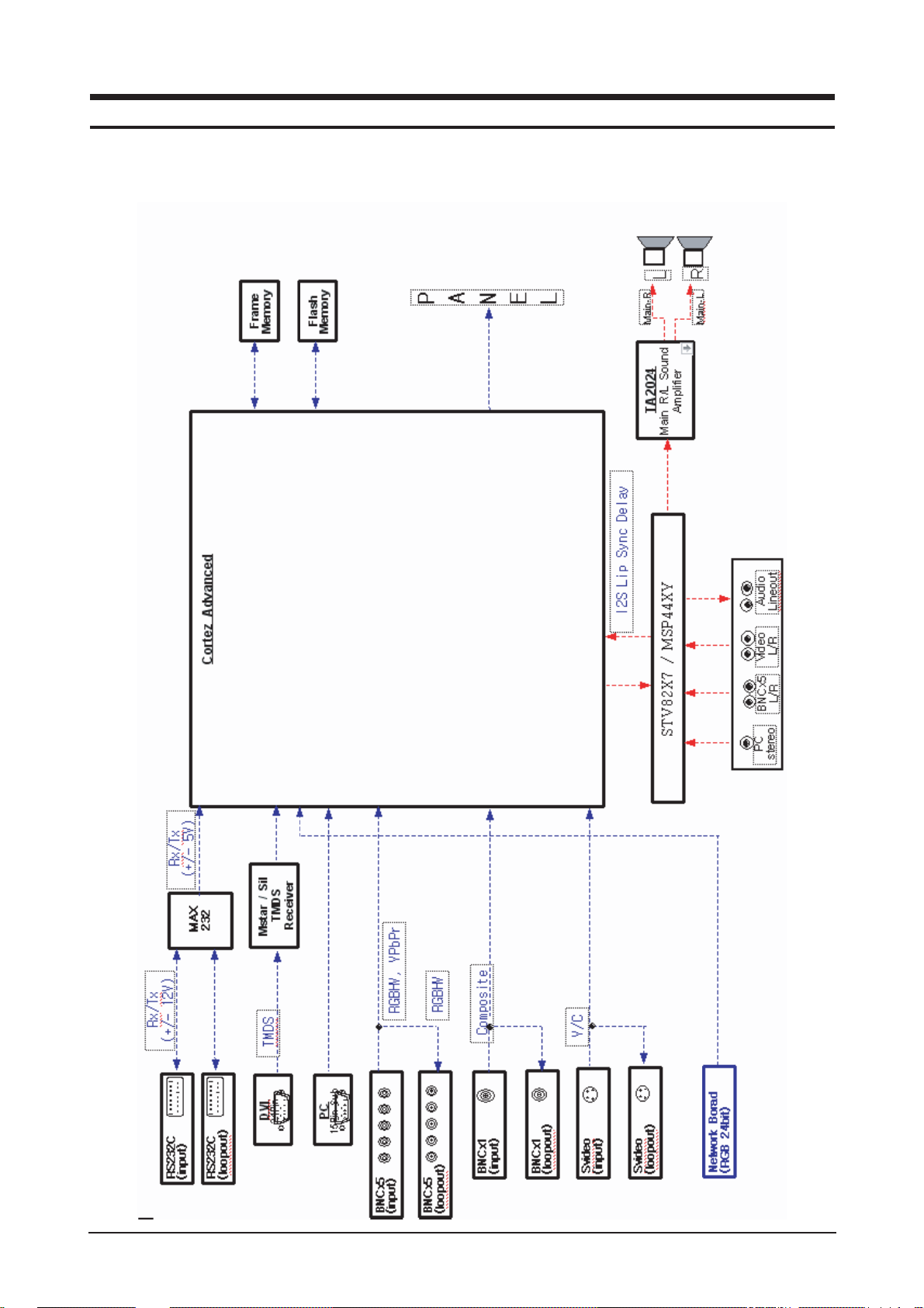
7 Block Diagrams
7-1
7 Block Diagram
- Document can not be used without Samsung's authorization.
7-1 Main Block
Page 73
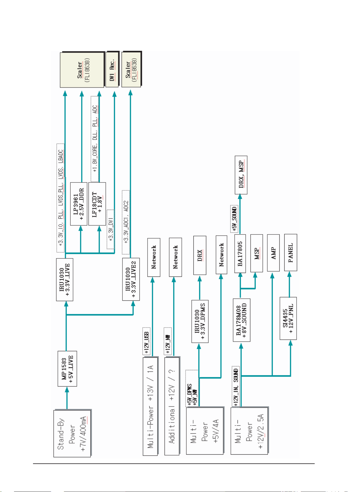
7 Block Diagrams
7-2
7-2-1 Main - Power Block
Page 74
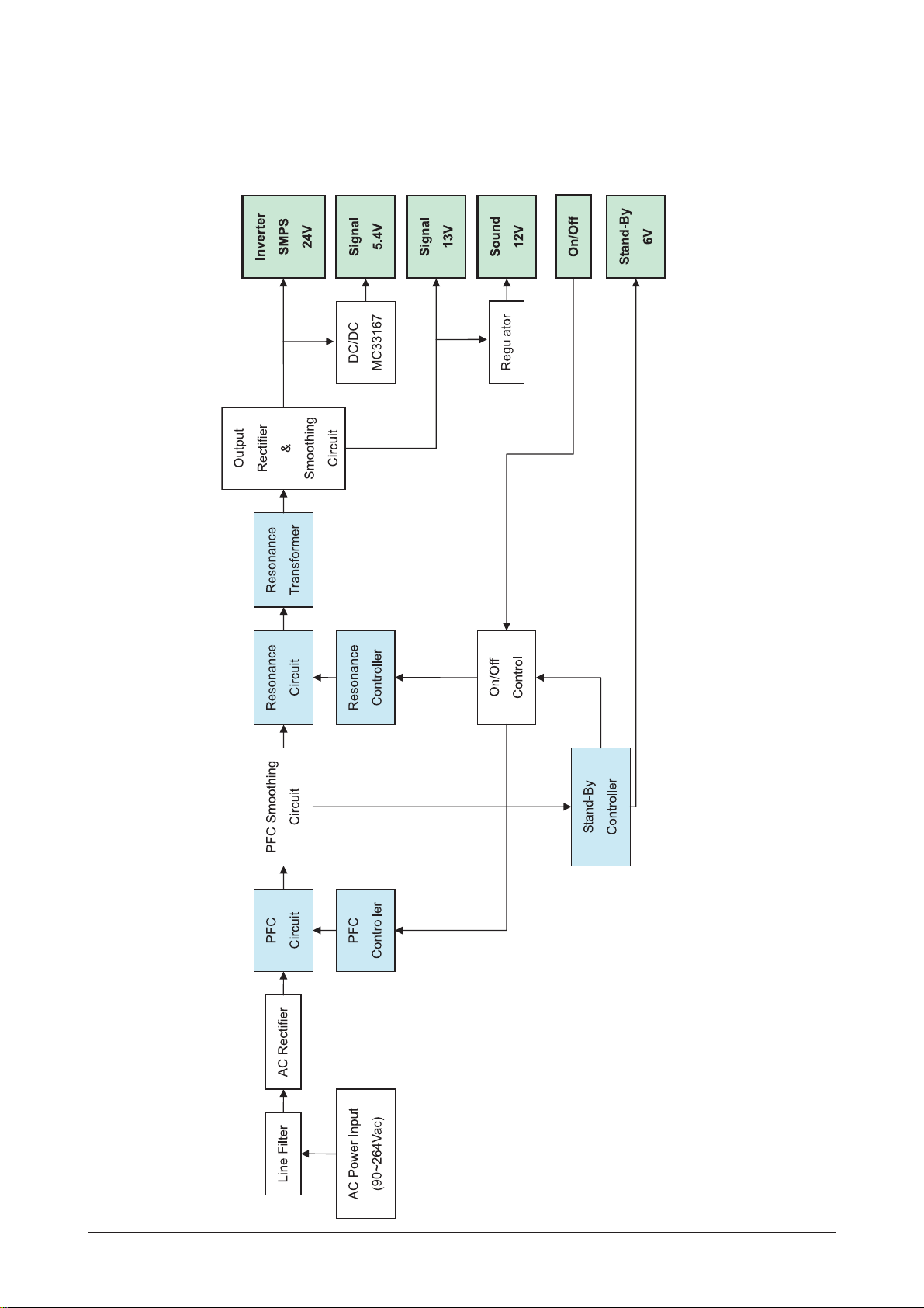
7 Block Diagrams
7-3
7-2 SMPS Board
Page 75

7 Block Diagrams
7-4
Memo
Page 76
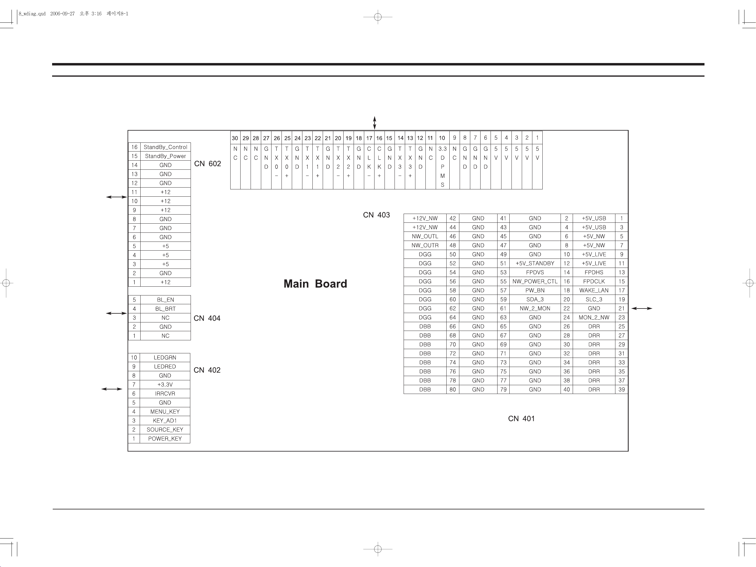
8-1
8 Wiring Diagram
8 Wiring Dia gr am
8-1 Main Board W iring Diag ram
LVDS Connector
(Connect to PANEL)
NETWORK
Board
Power Connector
(Connect to IP Board)
Power Connector
(Connect to SMPS)
Function
Page 77
8 Wiring Diagram
8-2
Memo
Page 78
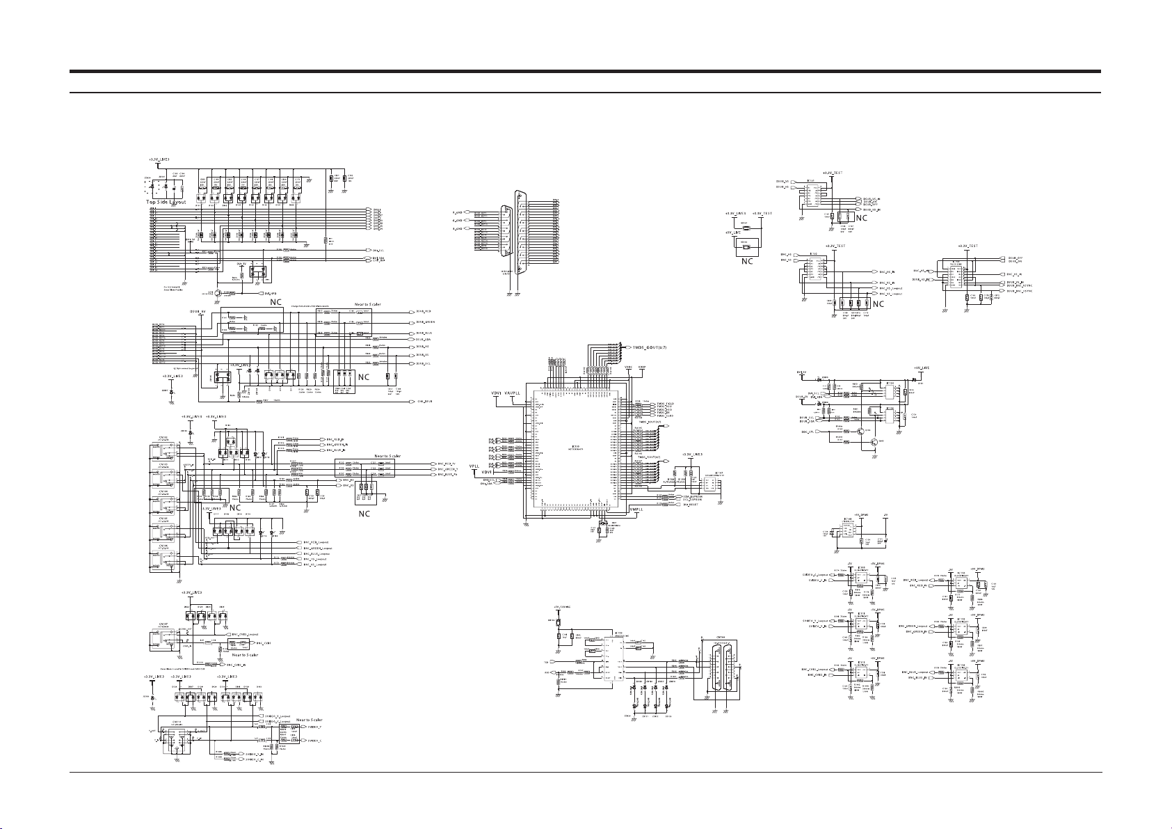
9-1
9 Schematic Diagram
9 Schematic Diagram
-This Document can not be used without Samsung ’s authorization.
9-1 Main board Schematics Diagram(Signal input)
Page 79
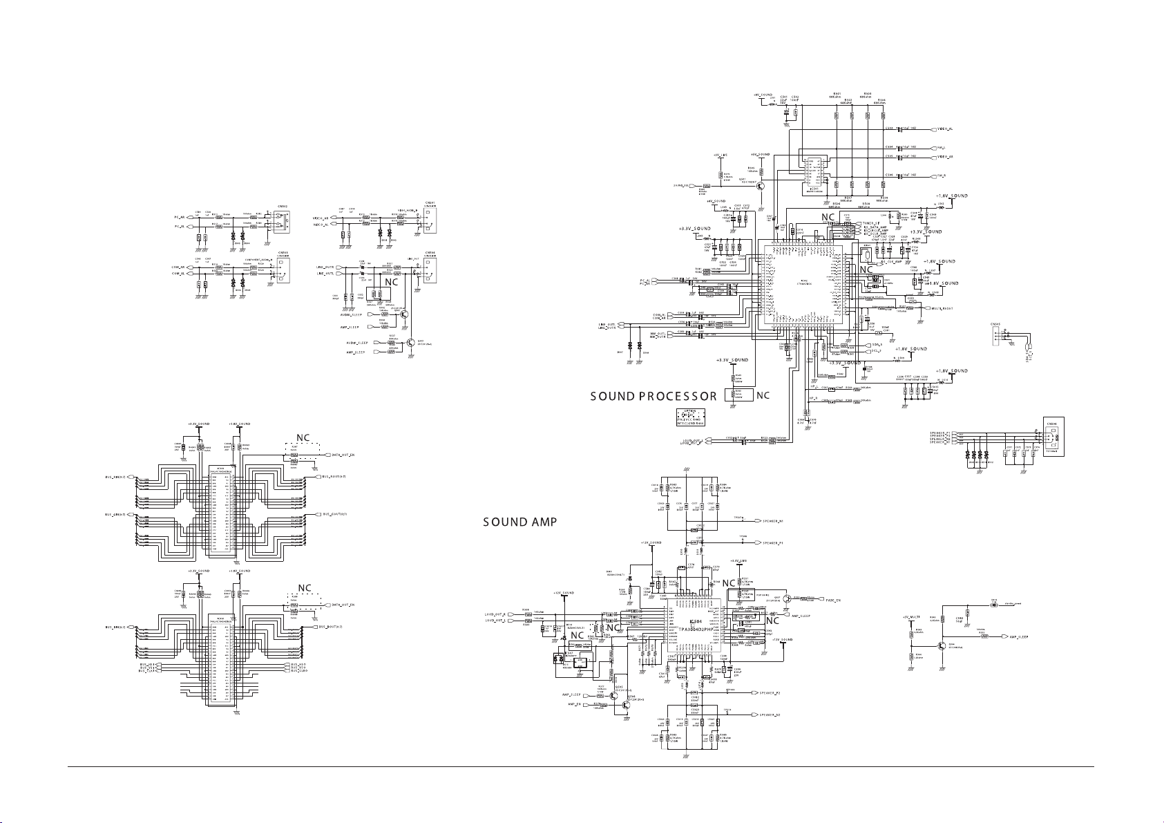
9 Schematic Diagram
9-2
9-1-2 Main board Schematics Diagram (SOUND)
Page 80
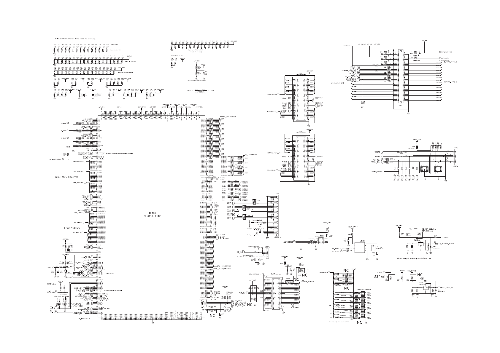
9-3
9 Schematic Diagram
9-1-3 Main board Schematics Diagram (SCALER)
Page 81
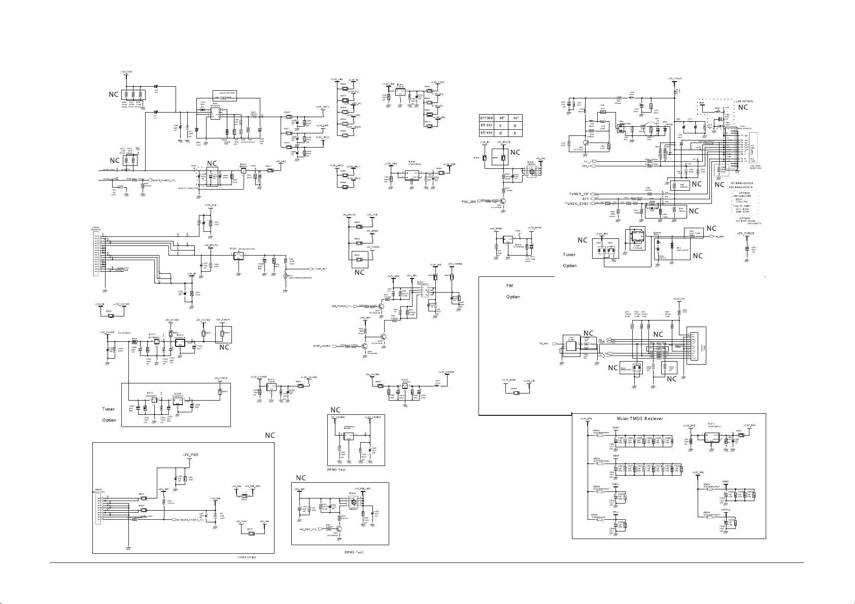
9 Schematic Diagram
9-4
9-1-4 Main board Schematics Diagram (Power & Tuner Option)
Page 82
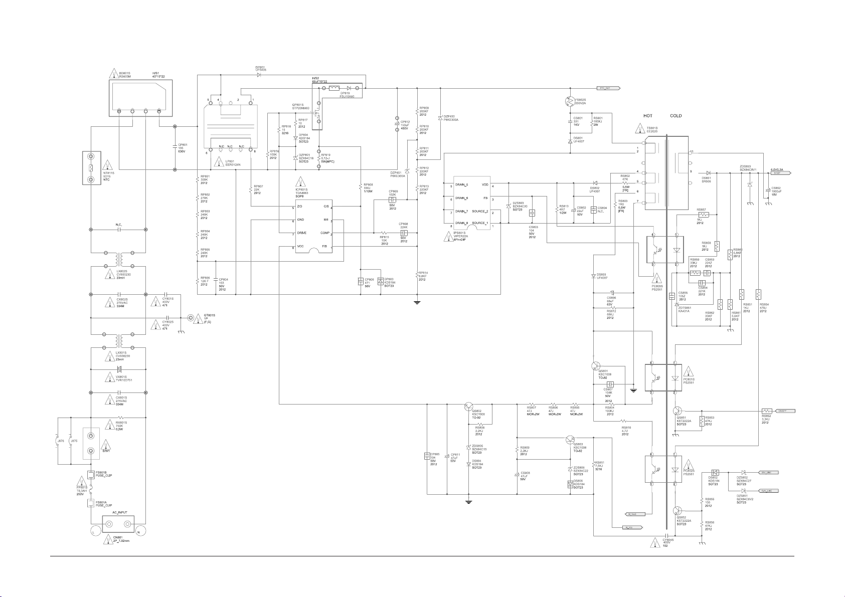
9-5
9 Schematic Diagram
9-1-5 SMPS Schematics Diagram (1)
Page 83
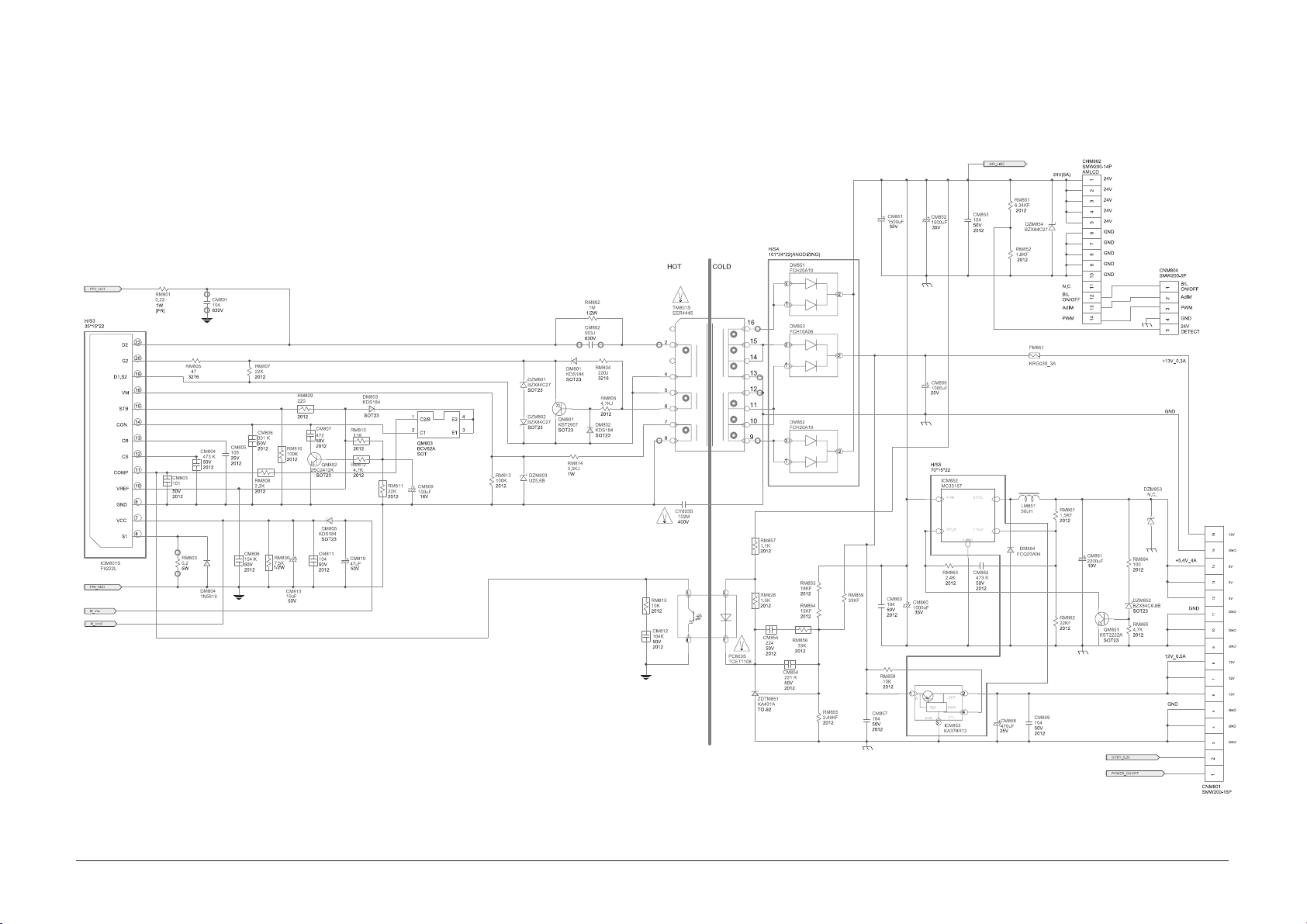
9 Schematic Diagram
9-6
9-1-6 SMPS Schematics Diagram (2)
Page 84
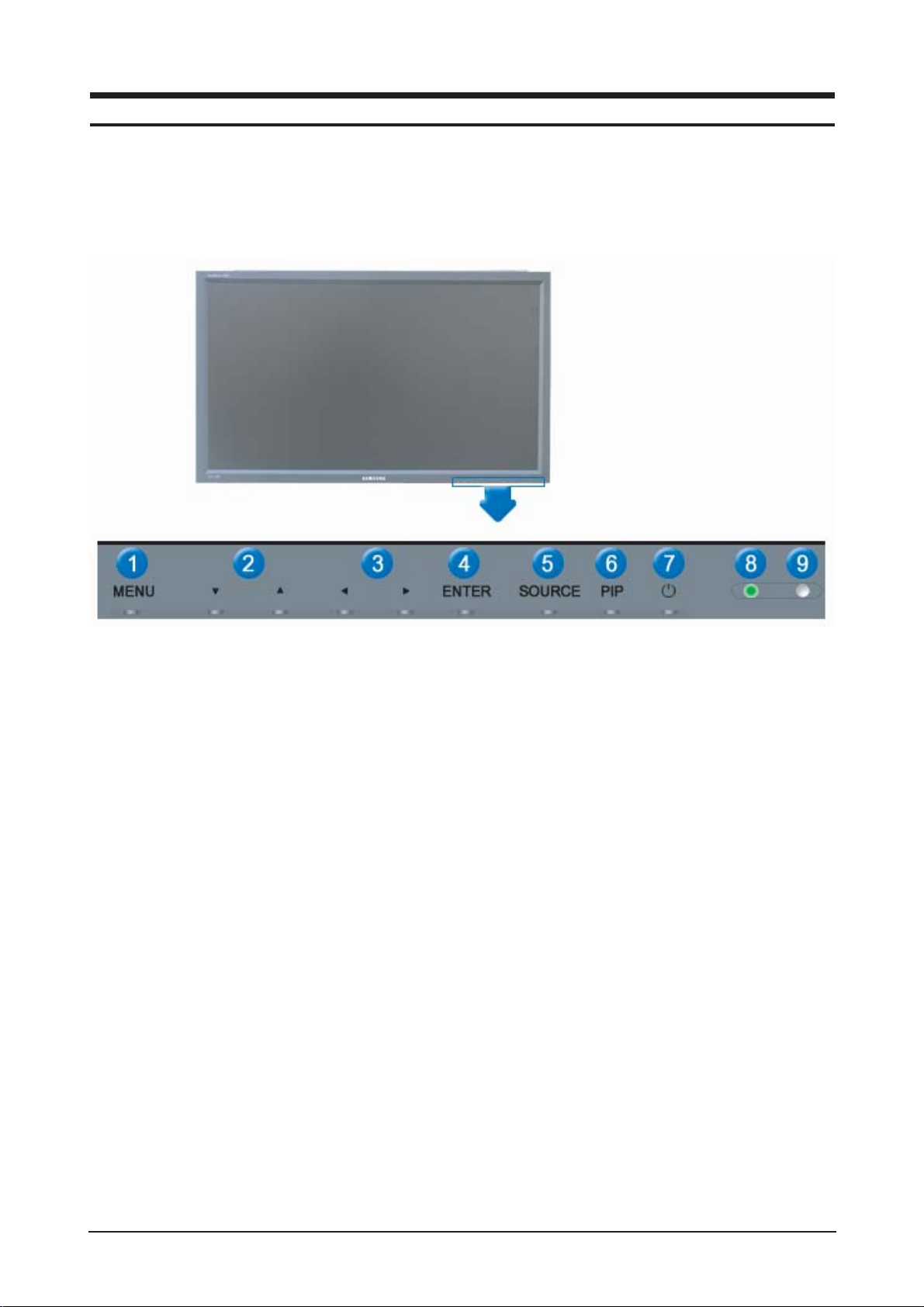
10 Operating Instructions and Installation
10-1
10 Operating Instructions and Installation
10-1 Front
1. MENU
2. Navigate button (Up-Down button)
3. Adjust button (Left-Right button)
Volume button
4. ENTER
5. SOURCE
6. PIP
7. Power button
8. Power indicator
9. Remote Control Sensor
MENU:
Use this button to open or exit the OSD menu or return to the previous menu.
Up-Down:
Moves from one menu item to another vertically or adjusts selected menu values.
Left-Right:
Moves from one menu item to another horizontally or adjusts selected menu values. Also use to adjust the
volume.
ENTER:
Activates a highlighted menu item.
SOURCE:
Selects the video signal. Changing the source is allowed only in devices that are connected to the monitor at
the time.
* Video Signal Changing Order
[PC] [BNC] [DVI] [AV] [S-Video] [Component] [MagicNet]
Page 85
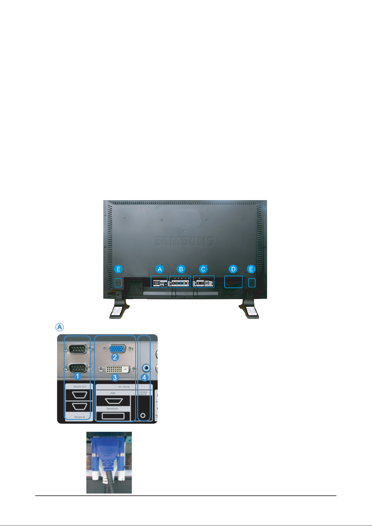
10-1-1 Rear
The monitor's rear configuration may vary slightly depending on the monitor model.
-Connection Terminal
1. RS232C OUT/IN (RS232C Serial Port)
: MDC(Multiple Device Control) Program Port
2. PC IN(RGB) (PC Video Connection Terminal)
: Using D-Sub (15 Pin) Cable - PC Mode (Analog PC)
3. DVI IN(HDCP) (PC Video Connection Terminal)
: Using DVI Cable (DVI-D to DVI-D) - DVI Mode (Digital PC)
4. PC/DVI/BNC AUDIO IN
(PC/DVI/BNC Audio Connection Terminal(Input))
10 Operating Instructions and Installation
10-2
PIP(Picture in Picture) :
Push the PIP button to turn PIP screen On/Off.
More than one PIP couldn't be overlapped on screen as BNC and the component use the same terminal.
- PC / DVI: AV / S-Videos / Component Mode
- BNC: AV / S-Video
- AV/ S-Video: PC / BNC / DVI Mode
- Component: PC / DVI Mode
POWER :
Use to turn the monitor on or off.
LED :
Lights up in normal mode. It blinks in green in Power Saver mode.
Remote Control Sensor:
Aim the remote control towards this spot on the Monitor.
Page 86
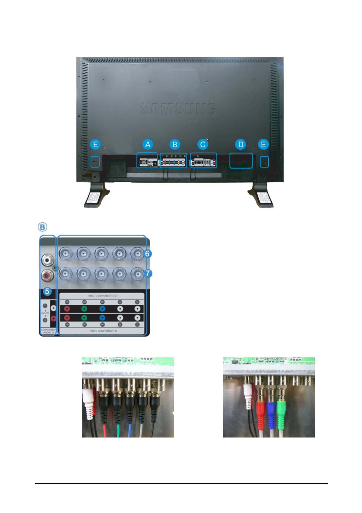
-Connection Terminal
10 Operating Instructions and Installation
10-3
5. COMPONENT AUDIO IN [L-AUDIO-R]
(Component Audio Connection Terminal (Input))
6. BNC/COMPONENT OUT
(BNC/Component Connection Terminal (Output))
- BNC (Analog PC) Connection :
connecting R, G, B, H, V port
- Component Connection :
connecting PR, Y, Pb port
7. BNC/COMPONENT IN
(BNC/Component Connection Terminal (Input))
BNC COMPONENT
Page 87
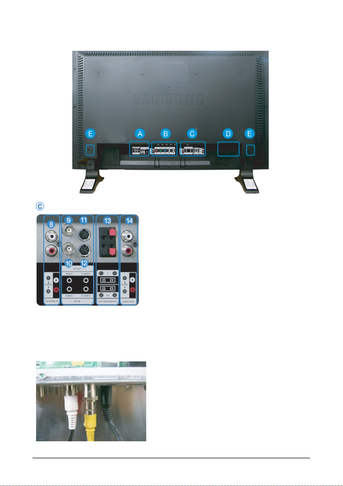
10 Operating Instructions and Installation
10-4
-Connection Terminal
8. AV AUDIO IN [L-AUDIO-R]
(Monitor Audio Connection Terminal (Input))
9. AV OUT [VIDEO] (Video Connection Terminal)
: AV mode (Output)
10. AV IN [VIDEO] (Video Connection Terminal)
: AV mode (Input)
11. AV OUT [S-Video] (S-Video Connection Terminal)
: S-Video mode (Output)
12. AV IN [S-Video] (S-Video Connection Terminal)
: S-Video mode (Input)
13. EXT SPEAKER(8 Ω ) (EXT Speaker Connection
Terminal)
14. AUDIO OUT [L-AUDIO-R]
(Monitor Audio Connection Terminal (Output))
: MONITOR OUT is the terminal for sound output of PC,
DVI or BNC
Page 88
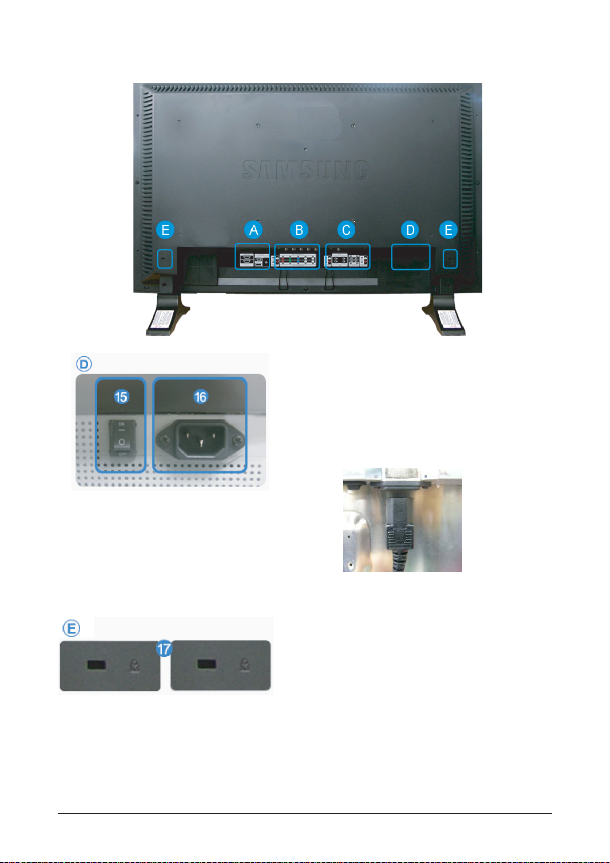
10 Operating Instructions and Installation
10-5
-Connection Terminal
15. POWER S/W
16. POWER IN
17. Kensington Lock
The Kensington lock is a device used to physically
fix the system when using it in a public place.
Page 89
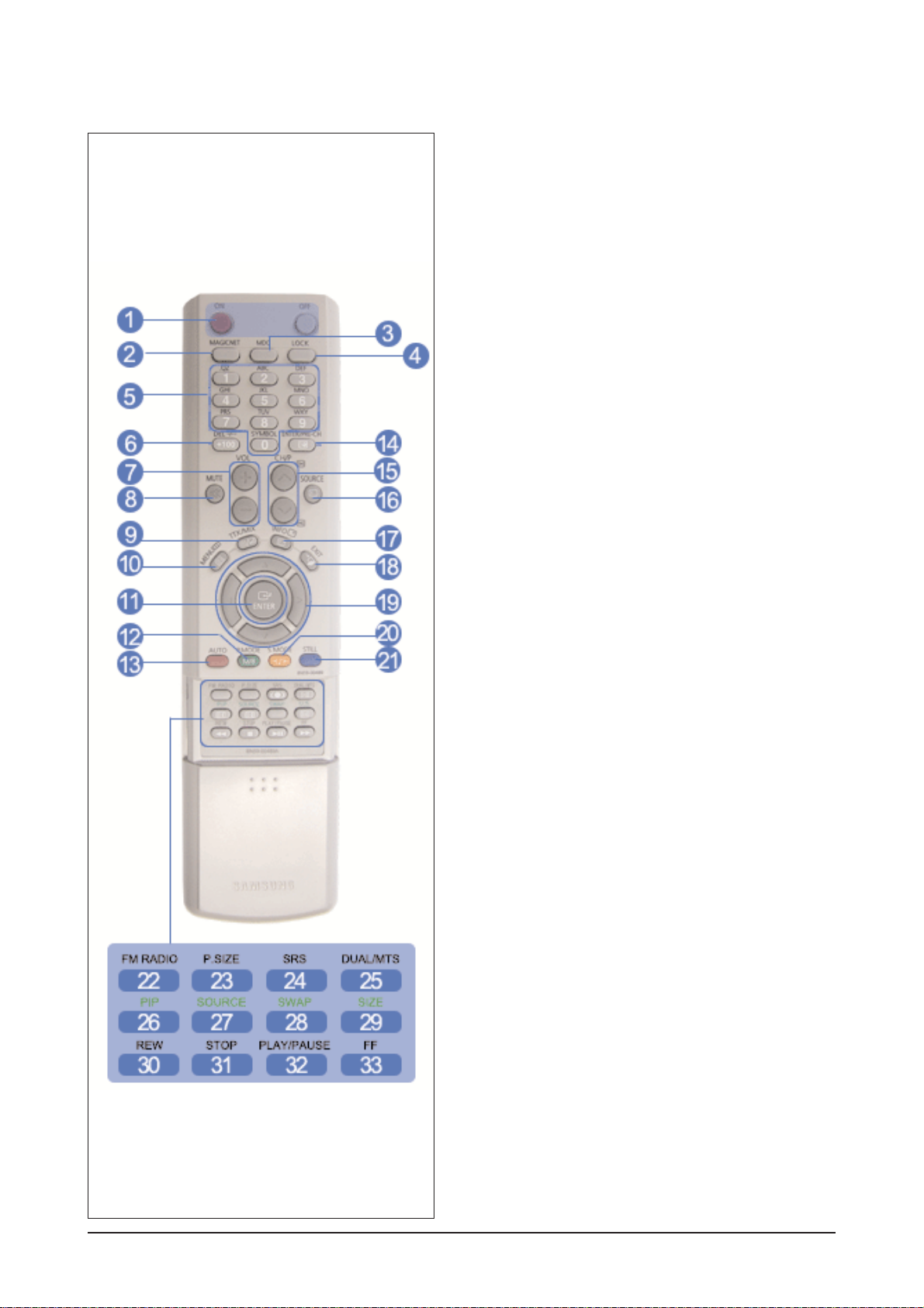
10 Operating Instructions and Installation
10-6
10-1-2 Remote Control
1) ON / OFF
Use these buttons to turn the monitor on or off.
2) MAGICNET
MagicNet Quick Launch Button.
3) MDC
MDC Quick Launch Button.
4) LOCK
This button will activate or deactivate all function
keys on both the remote control and the monitor
except for the Power and LOCK buttons.
5) MagicNet buttons
Used for MagicNet.
- Alphanumeric: Used to enter the Internet address.
- DEL: Functions as the backspace.
- SYMBOL: Used to enter the symbols. (.O_-:/)
- ENTER: Used to enter values.
6) +100
Press to select channels over 100.
For example, to select channel 121, press "+100",
then press "2" and "1".
[This fuction does not work for this monitor.]
7) VOL
Adjusts the audio volume.
8) MUTE
Pauses (mutes) the audio output temporarily.
Displayed on the lower left corner of the screen.
The audio resumes if MUTE or - VOL + is pressed
in the Mute mode.
9) TTX/MIX
TV channels provide written information services via
teletext.
[This function is available only in Europe. ]
10) MENU
Use this button to open the on-screen menu and
exit from the menu screen or close screen adjust
ment menu.
11) ENTER
Activate a highlighted menu item.
12) P.MODE
This button is used to return to the immediately pre
vious channel.
[This fuction does not work for this monitor.]
13) AUTO
Adjusts the screen display automatically.
If you change resolution in the control panel, auto
function will be executed.
Page 90

10-7
14) ENTER/PRE-CH
This button is used to return to the immediately
previous channel.
[This fuction does not work for this monitor.]
15) CH/P
In TV mode, selects TV channels.
16) SOURCE
Push this button to change video sources.
17) INFO
Current picture information displays on the
upper left corner of the screen.
18) EXIT
Exits from the menu screen.
19) Up-Down Left-Right buttons
Moves from one menu item to another
horizontally, vertically or adjusts selected menu
values.
20) S.MODE
When you press this button, current mode is
displayed on the lower center of the screen.
The monitor has a built-in high fidelity stereo
amplifier.
Then push button again to circle through
available preconfigured modes.
( Standard
→ Music → Movie → Speech →
Custom )
21) STILL
Operates only for the CVBS, S-Video and RF
Signal sources.
Press the button once to freeze the screen.
Press it again to unfreeze.
22) FM RADIO
Turns on/off FM Radio.
In PC/DVI mode, sets only SOUND to FM
Radio.
In general Video SOURCE mode, sets to FM
RADIO, turning off the screen.
In areas where signal is weak, noise may occur
while FM radio is broadcast.
23) P.SIZE
Press to change the screen size.
24) SRS
SRS
25) DUAL/MTS
DUALSTEREO/MONO, DUAL l / DUAL ll and
MONO/NICAM MONO/NICAM STEREO can be
operated depending on broadcasting type by
using DUAL button on the remote control while
watching TV.
MTSYou can select the MTS (Multichannel
Television Stereo) mode.
26) PIP
Every time you push the button, a PIP screen
appears.
27) SOURCE
The PIP window's signal source changes.
28) SWAP
Swapping the contents of the PIP and main
image.
The image in the PIP window will appear on the
main screen, and the main screen image will
appear in the PIP window.
29) SIZE
You can switch the Picture Size.
30) REW
Rewind
31) STOP
Stop
32) PLAY / PAUSE
Play/Pause
33) FF
Fast forward
3 Operating Instructions and Installation
Page 91
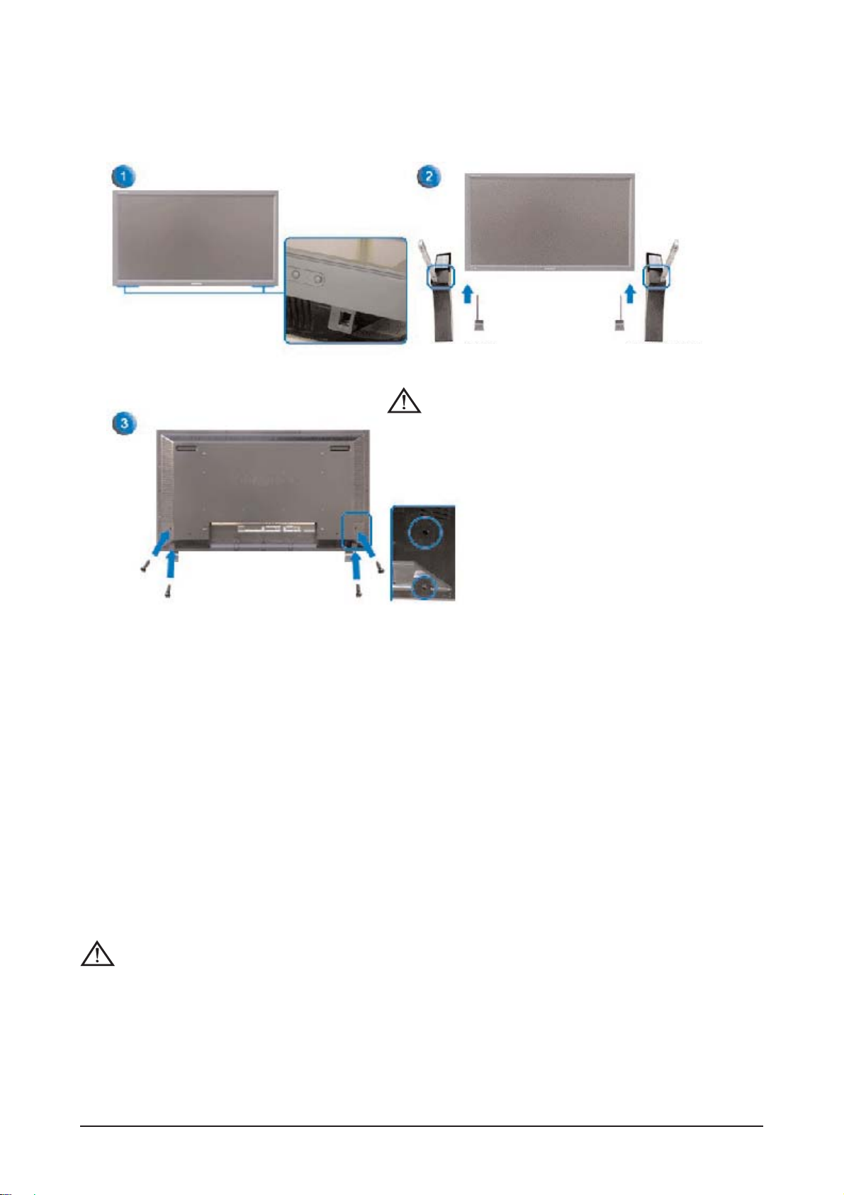
10 Operating Instructions and Installation
10-8
10-2 Installing Stand Kit
1. A 'Cover-Protector' is used to protect the hole at the bottom of the monitor, where the stand is inserted.
Be sure to remove the 'Cover-Protector' when attaching the provided Semi Stand or stand kit (sold
sepa rately) and cover the hole using the 'Cover-Hole' when attaching the wall mount kit.
2. Set up the left and right stands respectively.
3. Put the stand into the hole at the bottom of the monitor.
Insert screw into the hole indicated and tighten. (M4 × L15)
Left stand
Make sure to install the stand with Caution
label folded backward.
Right stand
Make sure to use the semi stand only for adjusting the screen.
The company is not responsible for the damage caused by using them with other purpose.
Page 92
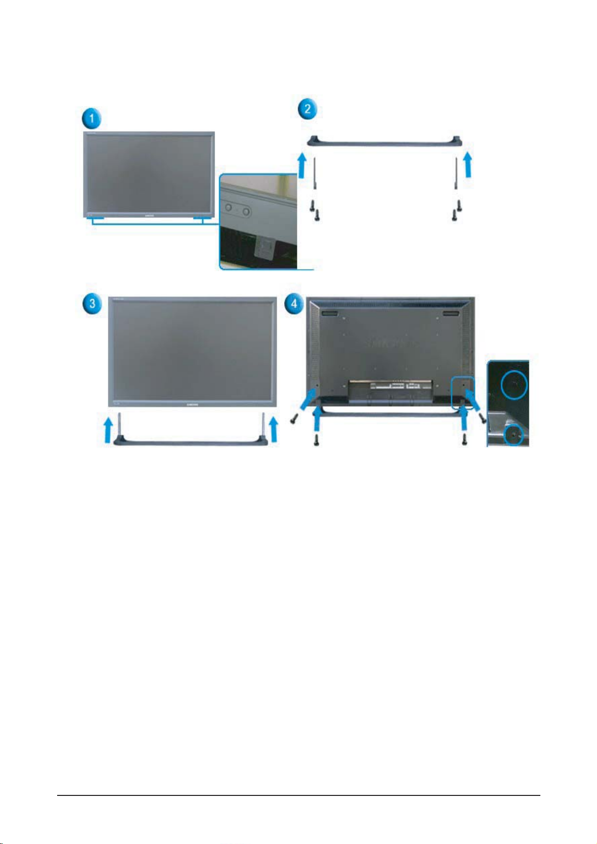
10 Operating Instructions and Installation
10-9
10-2-1 Installing Stand Kit (sold separately)
1. A 'Cover-Protector' is used to protect the hole at the bottom of the monitor, where the stand is inserted.
Be sure to remove the 'Cover-Protector' when attaching the provided Semi Stand or stand kit (sold sepa
rately) and cover the hole using the 'Cover-Hole' when attaching the wall mount kit.
2. Make sure you put the parts in the right direction and in the right place. (M4 × L15)
3. Put the stand into the hole at the bottom of the monitor.
4. Insert screw into the hole indicated and tighten. (M4 × L15)
Page 93

10 Operating Instructions and Installation
10-10
Memo
Page 94
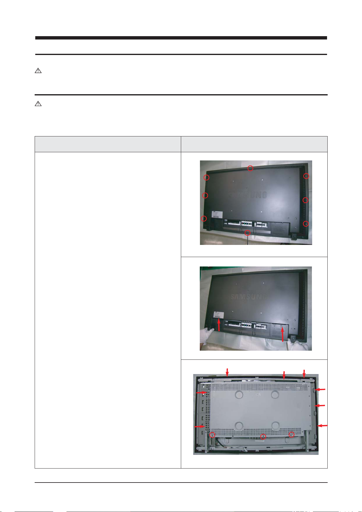
11 Disassembly and Reassembly
11-1
Description Picture Description
1. Place monitor face down on cushioned table.
Remove 8 screws from the rear cover.
Lift up the rear cover.
2. Remove 11 screws from the shield and lift up
the shield.
11-1 Disassembly
WARNING: This monitor contains electrostatically sensitive devices. Use caution
when handling these components.
Cautions: 1. Disconnect the monitor from the power source before disassembly.
2. Follow these directions carefully; never use metal instruments to pry apart the cabinet.
11 Disassembly and Reassembly
This section of the service manual describes the disassembly and reassembly procedures for the BE40TS LCD monitor.
Page 95
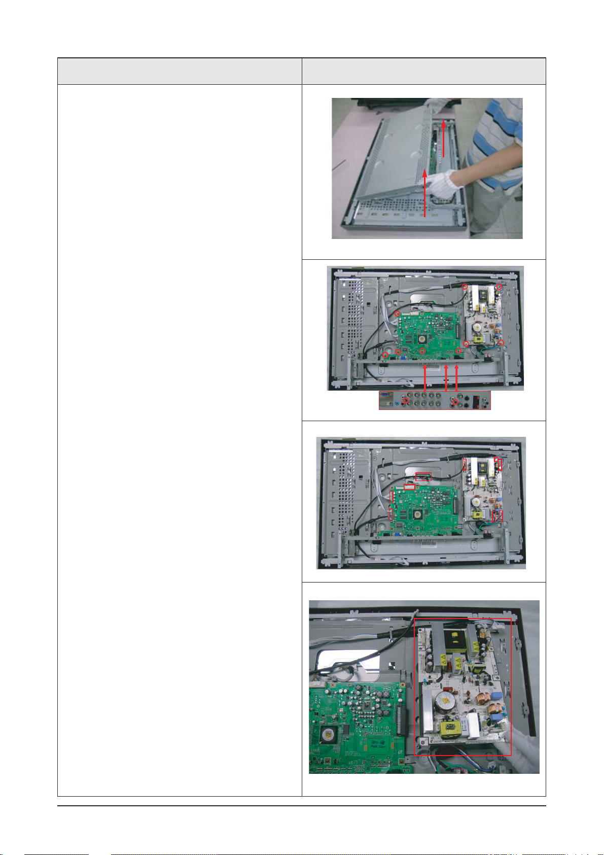
11 Disassembly and Reassembly
11-2
Description Picture Description
3. Remove the screws and cables as showed the
picture.
4. Separate the SMPS board and main board from
bottom BRKT as showed the picture.
(When changing panel only, not necessary to
separate boards but remove BRKT entirely.)
Page 96
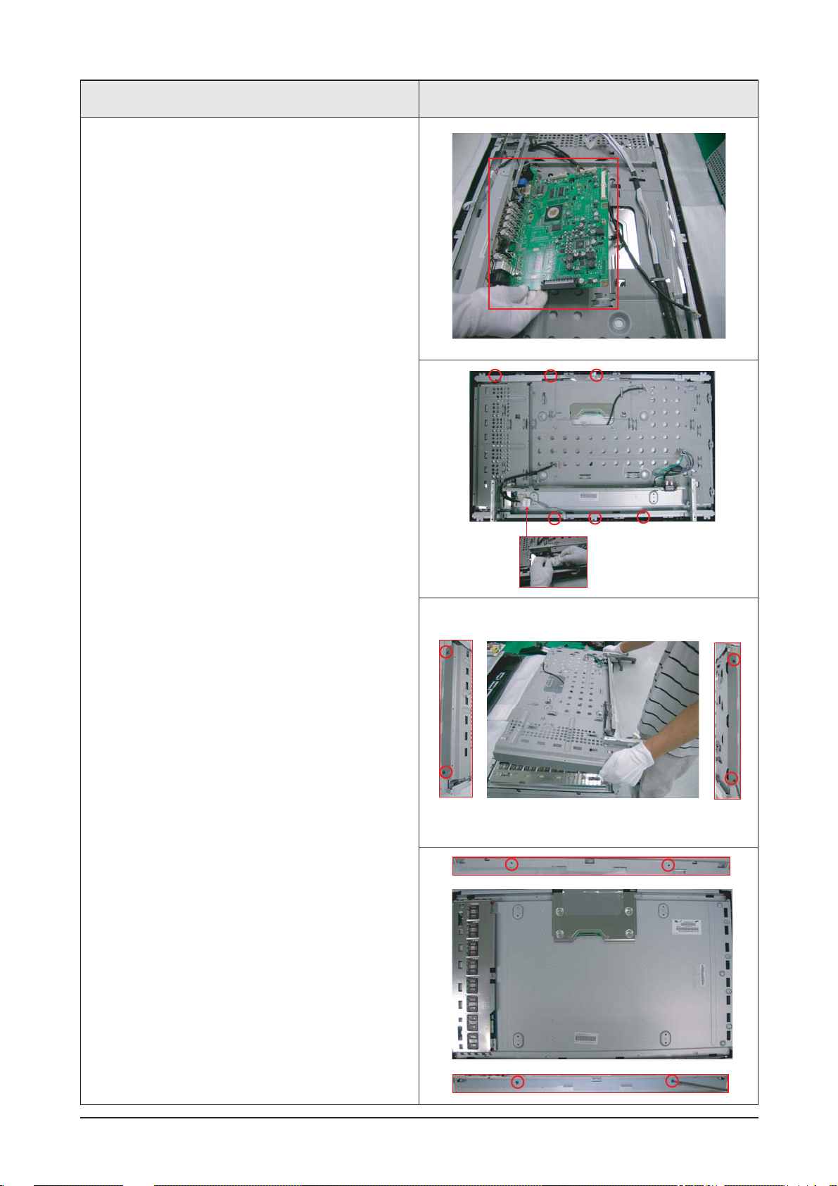
Description Picture Description
11 Disassembly and Reassembly
11-3
Description Picture Description
5. Remove the screws between side BRKT and
front cabinet, disconnect the cable of function
PCB as showed left picture, and lift up the panel.
6. Remove 4 screws (left-2, right-2) from side
BRKT, and lift up BRKT.
7. Remove the screws from side BRKT (top-2,
bottom-2), and separate panel and BRKTs.
Page 97

11 Disassembly and Reassembly
11-4
11-2 Reassembly
Reassembly procedures are in the reverse order of disassembly procedures.
Page 98
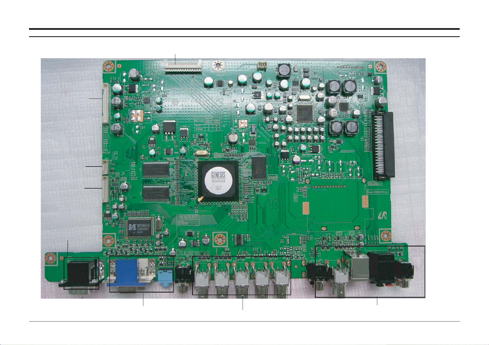
12 PCB layout
12-1
12 PCB layout
12-1 Main PCB layout
Power Connector
( Connect to the IP Board)
LVDS Connector
( Connect to the PANEL)
Power Connector
( Connect to the SMPS)
BNC/Component/Audio
PC (D-SUB/DVI/Audio)
RS232
Function
Speker/Audio out/Audio/AV/S-Video
Page 99
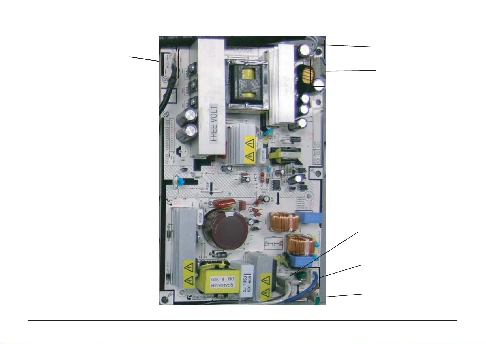
12 PCB layout
12-2
12-2 SMPS Board layout
Lamp Connector
(Connecting to panel inverter
- upper/left side)
Connecting to
AC socket
Power GND
Connecting to Mechanical switch
Power Connector
(Connecting to MAIN board,
Relation to Lamp control)
Power Connector
(Connecting to MAIN board)
Page 100
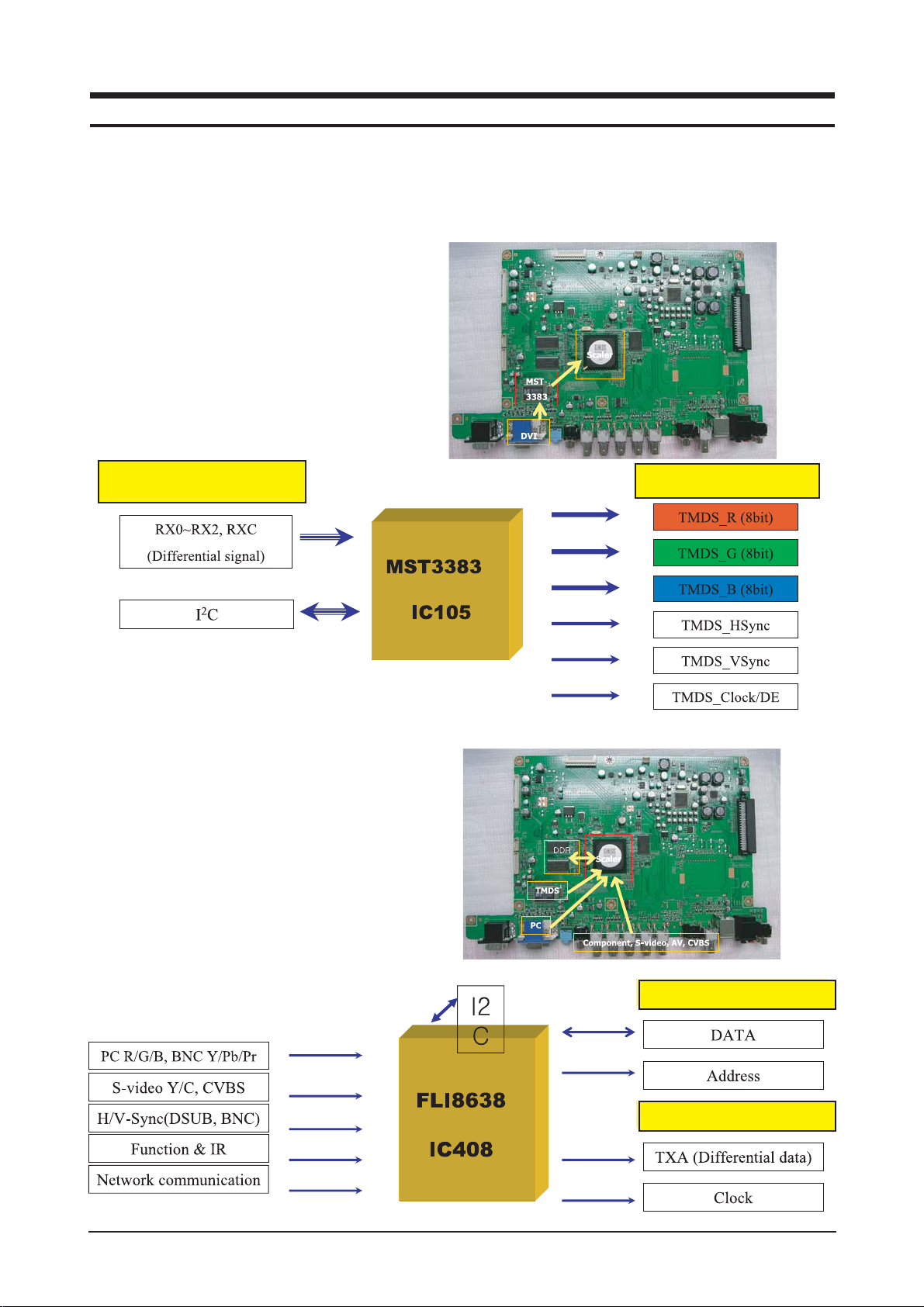
13 Circuit Descriptions
13-1
113
Circuit Descriptions
13-1 Main board par t
13-1-1 MST3383
- TMDS Receiver
- Convert the DVI input to the TMDS signal and send to the scaler.
13-1-2 FLI8638
- GENESIS Company Scaler IC
- Video decoder, micom, Image enhancer,
3-D Comb filter functions embedded
- Supports OSD and PIP
DVI input
FLI8638 input
HYB25D256 (DDR)
LVDS input
 Loading...