

Page 1

20-8910-0599
USER'S MANUAL
KS8910
100/10 Mbps Ethernet Transceriver(PHY)
Preliminary
Page 2

Important Notice
The information in this publication has been carefully
checked and is believed to be accurate at the time of
publication. Samsung assumes no responsibility,
however, for possible errors or omissions, or for any
consequences resulting from the use of the
information contained herein.
Samsung reserves the right to make changes to its
products or product specifications with the intent to
improve function or design at any time and without
notice and is not required to update this
documentation to reflect such changes.
This publication does not convey to a purchaser of
semiconductor devices described herein any license
under the patent rights of Samsung or others.
Samsung makes no warranty, representation, or
guarantee regarding the suitability of its products for
any particular purpose, nor does Samsung assume
any liability arising out of the application or use of any
product or circuit and specifically disclaims any and all
liability, including without limitation any consequential
or incidental damages.
KS8910 100/10 Mbps Ethernet Transceiver User’s Manual
Publication Number: 20-8910-0599
Publication Date: May 1999
1999 Samsung Electronics
"Typical" parameters can and do vary in different
applications. All operating parameters, including
"Typicals," must be validates for each customer
application by the customer’s technical experts.
Samsung products are not designed, intended, or
authorized for use as components in systems intended
for surgical implant into the body, for other applications
intended to support or sustain life, or for any other
application in which the failure of the Samsung product
could create a situation where personal injury or death
may occur.
Should the Buyer purchase or use a Samsung product
for any such unintended or unauthorized application,
the Buyer shall indemnify and hold Samsung and its
officers, employees, subsidiaries, affiliates, and
distributors harmless against all claims, costs,
damages, expenses, and reasonable attorney fees
arising out of, either directly or indirectly, any claim of
personal injury of death that may be associated with
such unintended or unauthorized use, even if such
claim alleges that Samsung was negligent regarding
the design or manufacture of said product.
All rights reserved. No part of this publication may be reproduced, stored in a retrieval system, or transmitted in any form or by
any means, electric or mechanical, by photocopying, recording, or otherwise, without the prior written consent of Samsung
Electronics.
Samsung Electronic’s microcontroller business has been awarded full ISO-14001
certification (BVQI Certificate No. 9330). All semiconductor products are designed and
manufactured in accordance with the highest quality standards and objectives.
Samsung Electronics Co., Ltd.
San #24, Nongseo-Ri, Kiheung-Eup
Yongin-City, Kyungi-Do, Korea
C.P.O. Box #37, Suwon 449-900
Phone: 82-331-209-3104
Fax: 82-331-209-3109
Internet: http://www.samsungsemi.com
Printed in the Republic of Korea
Page 3

Preface
The KS8910 100/10 Mbps Ethernet Transceiver User’s Manual is intended for application designers and
programmers who are using the KS8910 100/10 Mbps ethernet microcontroller for product development.
The first six sections of this manual give you a general orientation to the KS8910 100/10 Mbps ethernet
transceriver:
• Section 1 “Product Overview” introduces a product and describes features, PCI system, controller application
configurations.
• Section 2 “External Signals” describes external signal, pin assignments, and signals.
• Section 3 “Functional Blocks” describes functional block, MII, PCI bus, DMA function block, and MAC
functional block.
• Section 4 “100 Base-TX Digital Blocks”
• Section 5 “10 Base-T Digital Blocks”
• Section 6 “Analog Blocks”
• Section 7 “Registers”
• Section 8 “Electrical Characteristics”
• Section 9 “Application Note”
• Section 10 “Mechanical Data”
• Section 11 “Appendix”
PRELIMINARY SPECIFICATION
KS8910 100/10 Mbps ETHERNET CONTROLLER v
Page 4

PRELIMINARY SPECIFICATION
vi KS8910 100/10 Mbps ETHERNET CONTROLLER
Page 5

Table of Contents
Section 1 Product Overview
Introduction ............................................................................................................................................ 1-1
Features ................................................................................................................................................. 1-2
Ethernet 10Base-T and 100Base-TX Block Diagram .............................................................................1-3
Reference Documents .............................................................................................................................1- 4
Section 2 External Signals
Overview ................................................................................................................................................. 2-1
External Signals ...................................................................................................................................... 2-2
Pin Assignments ..................................................................................................................................... 2-3
Signal Descriptions ................................................................................................................................. 2-4
Section 3 Functional Blocks
MII data Interface .................................................................................................................................... 3-1
Management Agent ................................................................................................................................ 3-2
Power Management ................................................................................................................................ 3-2
Control Registers / Status Registers ....................................................................................................... 3-2
Auto-Negotiation ..................................................................................................................................... 3-2
100 Base-TX Digital Block ...................................................................................................................... 3-3
10Base-T Digital Block ........................................................................................................................... 3-5
100Base-TX and 10Base-T Analog Blocks ............................................................................................ 3-5
Section 4 100 Base-TX Digital Blocks
Overview ................................................................................................................................................. 4-1
Physical Coding Sublayer (PCS) ................................................................................................... 4-1
physical Medium Attachment Sublayer (PMA) ............................................................................... 4-2
Physical Medium Dependent Sublayer (PMD) ............................................................................... 4-2
Description of operation ................................................................................................................. 4-2
Physical Coding Sublayer (PCS) ............................................................................................................ 4-4
4B/5B Encoder, Decoder ............................................................................................................... 4-4
4B/5B Encoder (Transmit STM) ..................................................................................................... 4-6
4B/5B Decoder(Receive STM) ....................................................................................................... 4-6
Parallel and Serial Converters ....................................................................................................... 4-9
Carrier Sense ................................................................................................................................. 4-9
Physical Medium Attachment (PMA) ......................................................................................................4-10
Scrambling .....................................................................................................................................4-10
Link Monitor .................................................................................................................................... 4-12
NRZ to NRZI AND NRZI to NRZ ConversiON ............................................................................... 4-13
Physical Medium Dependent sublayer ................................................................................................... 4-14
PRELIMINARY SPECIFICATION
KS8910 100/10 Mbps ETHERNET CONTROLLER vii
Page 6

Table of Contents
Section 5 10 Base-T Digital Blocks
Overview .................................................................................................................................................5-1
Transmit Function ...................................................................................................................................5-1
Jabber Control Function .......................................................................................................................... 5-1
SQE Function .......................................................................................................................................... 5-3
Receive Function ....................................................................................................................................5-3
Polarity Reverse Function ..............................................................................................................5-3
Collision Detection Function ...........................................................................................................5-4
Loopback Function .................................................................................................................................. 5-5
Link Integrity Test..................................................................................................................................... 5-5
Section 6 Analog Blocks
Overview .................................................................................................................................................6-1
100Mbit/s Transmit Circuits .....................................................................................................................6-2
Frequency Synthesizer ................................................................................................................... 6-3
Crystal Oscillator ............................................................................................................................6-3
Transmit Twisted-Pair Driver ..........................................................................................................6-4
100Mbit/s Receive Circuits ......................................................................................................................6-5
Receiver Buffer ............................................................................................................................... 6-5
Adaptive Equalizer ..........................................................................................................................6-6
Base Line Restore ..........................................................................................................................6-6
Clock Recovery ..............................................................................................................................6-6
10Mbit/s transmit circuits .........................................................................................................................6-7
Transmit Wave Shaper ...........................................................................................................................6-7
10MBit/s Receive Circuits .......................................................................................................................6-7
Receiver .........................................................................................................................................6-7
Section 7 Registers
Overview .................................................................................................................................................7-1
Register Definitions ................................................................................................................................. 7-2
PHY registers ..........................................................................................................................................7-3
Base Mode Control : register 0 ....................................................................................................... 7-3
base mode status : register 1 ......................................................................................................... 7-5
PHY identifier 1 : register 2 .............................................................................................................7-6
PHY identifier 2 : register 3 .............................................................................................................7-6
Auto-negotiation Advertisement : Register 4 ..................................................................................7-7
Auto-negotiation Link Partner Ability : Register 5 ...........................................................................7-8
Auto-negotiation Expansion : Register 6 ........................................................................................ 7-9
Auto-negotiation Next Page Transmit Register : Register 7 ........................................................... 7-10
10Base-T Control Register : Register 16 ........................................................................................7-11
100Base-TX Control Register : Register 17 ...................................................................................7-12
PHY Address Register : Register 18 .............................................................................................. 7-12
Map Table Register 0 : Register 19 ................................................................................................ 7-13
Map Table Register 1 : Register 20 ................................................................................................ 7-13
Analog Control Register 0 : Register 21 .........................................................................................7-14
PRELIMINARY SPECIFICATION
viii KS8910 100/10 Mbps ETHERNET CONTROLLER
Page 7

Table of Contents
Analog Control Register 1 : Register 22 ......................................................................................... 7-14
Analog Status Register : Register 23 ............................................................................................. 7-15
10base-t Status Register : Register 24 .......................................................................................... 7-15
100base-t Status Register : Register 25 ........................................................................................ 7-16
Section 8 Electrical Characteristics
Absolute Maximum Ratings .................................................................................................................... 8-2
Recommended Operating Ranges ......................................................................................................... 8-2
D.C Electrical Characteristics .................................................................................................................8-3
MII PADS Specification .................................................................................................................. 8-3
100base-tx transceiver Specification ............................................................................................. 8-3
10base-t transceiver characteristics ............................................................................................... 8-4
Timming .................................................................................................................................................. 8-5
OSC clock frequency ..................................................................................................................... 8-5
MII-transmit clock Tolerance .......................................................................................................... 8-5
MII-Receive clock Tolerance .......................................................................................................... 8-6
MII/10base-T Transmit Timing .......................................................................................................8-7
MII/10base-T receive Timing .......................................................................................................... 8-8
MII/100Base-TX Transmit Timing .................................................................................................. 8-9
MII/100Base-TX receive Timing ..................................................................................................... 8-10
MII-Management Interface Timing ................................................................................................. 8-11
POWER on Reset Timming ........................................................................................................... 8-12
10Base-T SQE(Heartbeat) Timing ................................................................................................. 8-13
10Base-T Jabber Timing ................................................................................................................ 8-14
10Base-T Normal Link Pulse Timing .............................................................................................. 8-15
Auto- Negotiation And Fast Link Pulse Timing ............................................................................... 8-16
Section 9 Application Notes
NIC Applications ..................................................................................................................................... 9-1
KS9820 MAC Ethernet Controller Application ............................................................................... 9-1
Section 10 Mechanical Data
Package Dimension ................................................................................................................................ 10-1
Section 11 Appendix
Glossary .................................................................................................................................................. 11-1
Ethernet and Networking Acronyms and Terms ............................................................................ 11-1
PRELIMINARY SPECIFICATION
KS8910 100/10 Mbps ETHERNET CONTROLLER ix
Page 8

List of Figures
Figure Number Title Page Number
1-1 KS8910 PHY Transceiver (64-QFP-1414 Package) .........................................................1-1
1-2 Ethernet System Overview Diagram with Emphasis on MDI .............................................1-3
1-3 100/10 Mbps Ethernet Transceiver Block Diagram ........................................................... 1-3
2-1 External Signals .................................................................................................................2-2
2-2 KS8910 Pin Assignments ..................................................................................................2-3
3-1 Functional Block Diagram of KS8910 ................................................................................3-1
3-2 100Base-TX Digital Block of KS8910 ................................................................................. 3-3
3-3 Analog Blocks of KS8910 ..................................................................................................3-5
4-1 100Base-TX Operational Block Diagram of KS8910 ......................................................... 4-3
4-2 PCS Functional Block Diagram of KS8910 .......................................................................4-4
4-3 4B/5B Encoder (Transmit) State Diagram of KS8910 .......................................................4-7
4-4 5B/4B Decoder (Receive) State Diagram of KS8910 ........................................................4-8
4-5 Linear Feedback Shift Register (LFSR) .............................................................................4-10
4-6 Scrambler Function of KS8910 ..........................................................................................4-10
4-7 Descramble Function of KS8910 ....................................................................................... 4-11
4-8 Link Monitor State Diagram of KS8910 .............................................................................4-12
4-9 NRZ to NRZI Conversion of KS8910 ................................................................................. 4-13
5-1 State Diagram of Jabber Control Function ........................................................................5-2
5-2 SQE Function ....................................................................................................................5-3
5-3 State Diagram of Collision Detection Function .................................................................. 5-4
5-4 State Diagram of Link Integrity Test Function ...................................................................5-5
6-1 100Mbit/s Data Path Block Diagram of KS8910 ................................................................ 6-1
6-2 Analog Blocks of KS8910 ..................................................................................................6-2
6-3 Crystal Oscillator Connection ............................................................................................6-3
6-4 Transmit Twister-Pair Driver and Transmit Transformer ...................................................6-5
6-5 Receive Buffer Circuit Configuration .................................................................................6-6
8-1 Clock Frequency Timing Diagram .....................................................................................8-5
8-2 MII-Transmit Clock Tolerance Timing Diagram ................................................................. 8-5
8-3 MII-Receive Clock Tolerance Timing Diagram .................................................................. 8-6
8-4 MII/10Base-T Transmit Timing Diagram ............................................................................8-7
8-5 MII/10Base-T Receive Timing Diagram .............................................................................8-8
8-6 MII/100Base-TX Transmit Timing Diagram .......................................................................8-9
8-7 MII/100Base-TX Receive Timing Diagram ........................................................................8-10
8-8 MII-Management Interface Timing Diagram ......................................................................8-11
8-9 Power On Reset Timming Diagram ...................................................................................8-12
8-10 10Base-T (SQE)Heartbeat Timing Diagram ...................................................................... 8-13
8-11 10Base-T Jabber Timing Diagram .....................................................................................8-14
8-12 10Base-T Normal Link Pulse Timing Diagram ..................................................................8-15
8-13 Auto-Negotiation and Fast Link Pulse Timing Diagram ..................................................... 8-16
9-1 KS8910 (64-QFP-1414) Schematic Diagram with KS8920 ............................................... 9-1
10-1 KS8910 Package Dimension (64-QFP-1414) Type ...........................................................10-1
PRELIMINARY SPECIFICATION
x KS8910 100/10 Mbps ETHERNET CONTROLLER
Page 9

List of Tables
Table Number Title Page Number
2-1 KS8910 Signal Descriptions .............................................................................................. 2-4
4-1 4B/5B Coding of KS8910 .................................................................................................. 4-5
4-2 5B/4B Outputs.................................................................................................................... 4-6
6-1 Transmit Clocks Generated by the Frequency Synthesizer .............................................. 6-4
7-1 Address Mapping ..............................................................................................................7-2
8-1 Absolute Maximum Ratings (TA = 25 ° C) .......................................................................... 8-2
8-2 Recommended Operating Conditions ............................................................................... 8-2
8-3 MII Pads Specification ....................................................................................................... 8-3
8-4 100Base-TX Transceiver Specification ............................................................................. 8-3
8-5 10Base-T Transceiver Specification ................................................................................. 8-4
8-6 Clock Frequency ...............................................................................................................8-5
8-7 MII-Transmit Clock Tolerance ........................................................................................... 8-5
8-8 MII-Receive Clock Tolerance ............................................................................................ 8-6
8-9 MII/10Base-T Transmit Timing .......................................................................................... 8-7
8-10 MII/10Base-T Receive Timing ........................................................................................... 8-8
8-11 MII/100Base-TX Transmit Timing ..................................................................................... 8-9
8-12 MII/100Base-TX ReceiveTiming ....................................................................................... 8-10
8-13 MII-Management Interface Timing ....................................................................................8-11
8-14 10Base-T SQE(Heartbeat) Timing .................................................................................... 8-13
8-15 10Base-T Jabber Timing ................................................................................................... 8-14
8-16 10Base-T Normal Link Pulse Timing ................................................................................. 8-15
8-17 10Base-T Jabber Timing ................................................................................................... 8-16
PRELIMINARY SPECIFICATION
KS8910 100/10 Mbps ETHERNET CONTROLLER xi
Page 10
Preliminary Spec. ver 1.4
KS8910 100/10 Mbps ETHERNET TRANSCEIVER PRODUCT OVERVIEW
1 PRODUCT OVERVIEW
INTRODUCTION
The KS8910 10Base-T/100Base-TX Ethernet transceiver is fully compliant with the IEEE 802.3u specification,
provides configurable 100Mbs support for Category 5 unshielded twisted pair (UTP) and supports 10Mbs operation
on Category 3 UTP or Category 5 UTP. The transceiver provides an electrical interface between the Media
Independent Interface (MII) of the Media Access Controller (MAC) and the physical wire pair, and includes support
for the basic and extended register set of station management registers.
The Transceiver provides compatibility with full-duplex Ethernet and Fast Ethernet networks making it suitable for
applications such as switched hubs. Advanced features include Auto-Negotiation for enabling automatic
configuration of network characteristics as well as automatic power-down mode for reduced power consumption.
Functions provided by the transceiver include encoding and decoding of the serial data stream and delimiters, level
conversion, collision detection, signal quality error and link integrity testing, jabber control, and loopback testing.
The device also provides outputs for receive, transmit, collision, speed and link test LEDs.
The new 100-Mbit/s implementation of Ethernet increases the capacity of a network by a factor of ten while using
existing twisted-pair wiring. By maintaining the Media Access Control (MAC) layer and the CSMA/CD protocol
unchanged, network administrators can quickly deploy newer and faster implementations. This approach also
lowers cost of deployment since it allows re-use of existing software applications while supporting both 100- and
10-Mbit/s speeds, and new products may be deployed into transition markets.
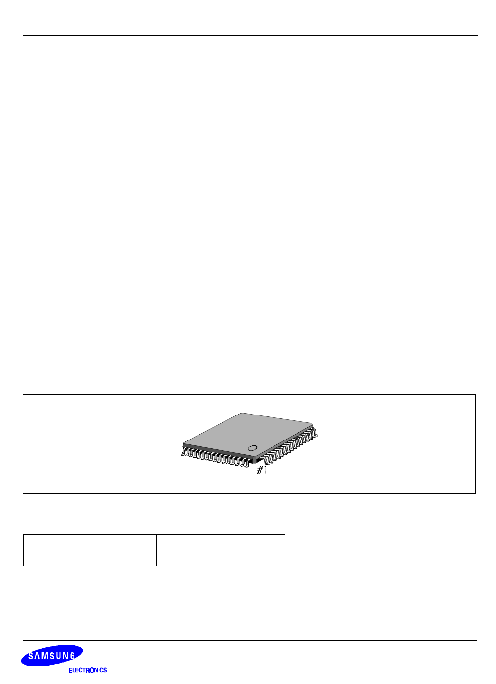
Figure 1-1. KS8910 PHY Transceiver (64-QFP-1414 Package)
Ordering Information
Device Package Operating Temperature
KS8910 64-QFP-1414 From 0 ° C to + 70 ° C
Applications
• 10BASE-T/100BASE-TX Network-ready PCs Interface, 10/100 Switches, Switched hubs
1-1
Page 11

Preliminary Spec. ver 1.4
PRODUCT OVERVIEW KS8910 100/10 Mbps ETHERNET TRANSCEIVER
FEATURES
• Support for old and new media : Compatible with existing 10-Mbit/s networks.
• 10BASE-T/100-BASE-TX operation : Range of price/performance points, Phased Conversion
• Full IEEE 802.3 compatibility : Compatible with existing hardware and software.
• Standard CSMA/CD,Full duplex capability at 10 and 100 Mbit/s : Increase in data throughput performance.
• Power management : Reduces power dissipation
• CMOS process with Single 3.3 volt operating supply : Compatible with standard system power supplies.
• On-chip filtering : Providing integrated lower cost solution
• Manual or automatic negotiation of port configuration : Provides ease of use in a mixed 10/100 Mbit/s network
configuration
• MII compliant interface : Can be used with many 100Base-TX MACs.
• Built-in transmit and receive filtering for 10BASE-T and 100BASE-TX
• Built-in LED drivers
ETHERNET SYSTEM BLOCK DIAGRAM
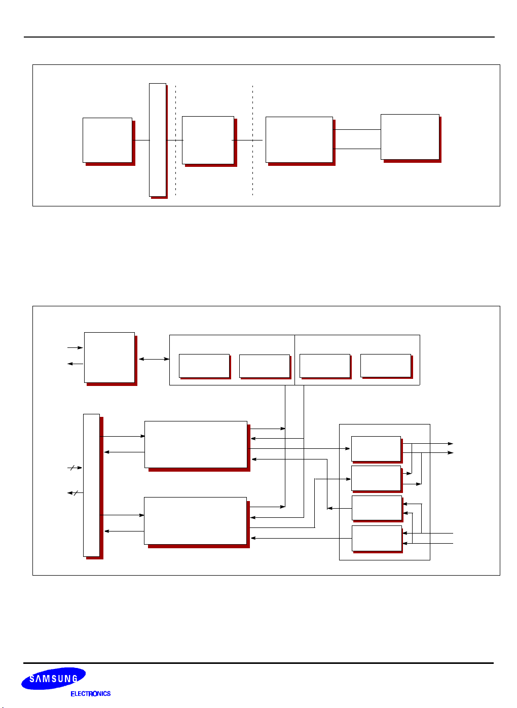
The complete Ethernet subsystem shown in Figure1-2 is divided into three sections:
• The system bus interface and Direct Memory Access (DMA) engine
• The Media Access Control (MAC) layer
• The Physical or Medium Dependent Interface (MDI) layer
The PCI bus interface section contains transmit and receive data buffering, DMA control buffering, and a register
access module buffering.
The MAC layer consists of transmit and receive blocks, a Content Addressable Memory (CAM) for address
recognition, along with control, status, and error counter registers.
This representative PCI-based 100/10-Mbit/s Ethernet controller supports the Media Independent Interface (MII).
The MII is a standard for a media-independent layer which separates physical-layer issues from the MAC layer.
The MII is part of the ISO approved IEEE 802.3 100-Base-T standard for 100 Mbit/s Ethernet.
This specification describes a single chip which implements a Physical or MDI layer capable of accepting 100/10
Mbit/s Ethernet signals that provides a Media Independent Interface (MII) for connectivity to the MAC layer. It is
intended as an interface specification and an architectural overview of the device and its operation.
1-2
Page 12
Preliminary Spec. ver 1.4
KS8910 100/10 Mbps ETHERNET TRANSCEIVER PRODUCT OVERVIEW
P
Processor
C
I
B
U
S
10/100Mbps
MAC
MII
10/100Mbps
PHY
10Base-T
Transformer
100Base-TX
KS8920
KS8910
Figure 1-2. Ethernet System Overview Diagram with Emphasis on MDI
ETHERNET 10BASE-T AND 100BASE-TX BLOCK DIAGRAM
MDC
MDIO
4
TX
4
RX
MI
Station
MGM
Interface
Mll Data Interface
Registers
Control
Registers
10/20MHz
10 Base-T
25MHz/125MHz
Fast Ethernet
100 Base-TX
20MHz
Status
Registers
Auto-Negotiation
Power
Management
Link Status
Link Control
Auto-neg
Arbitration
Driver
MLT3
Driver
10RX
100RX
20MHz
TX
RX
+
-
+
-
Figure 1-3. 100/10 Mbps Ethernet Transceiver Block Diagram
1-3
Page 13

Preliminary Spec. ver 1.4
PRODUCT OVERVIEW KS8910 100/10 Mbps ETHERNET TRANSCEIVER
REFERENCE DOCUMENTS
Supplement to ANSI/IEEE Std 802.3, 1993 Edition. Supplement to Carrier Sense Multiple Access with Collision
Detection (CSMA/CD) Access Method & Physical Layer Specifications: “MAC Parameters, Physical Layer, Medium
Attachment Units and Repeater for 100 Mb/s Operation”
Document # 802.3u / D5.3. June 14, 1995. This document has been approved, and is being submitted for
publication. This document has also been submitted and approved as an ISO/IEC standard.
International Standard ISO/IEC 8802-3: 1993(E), ANSI/IEEE Std 802.3. information technology--Local and
metropolitan area networks--Part 3: Carrier sense multiple access with collision detection (CSMA/CD) access
method and physical layer specifications: Fourth Edition, July 8, 1993.
FDDI Twisted Pair Physical Layer Medium Dependent (TP-PMD). ANSI T12/94-X3T9.5/93-TP-PMD/312 Rev 2.1.
March, 1994.
1-4
Page 14

Preliminary Spec. ver 1.4
KS8910 100/10 Mbps ETHERNET TRANSCEIVER EXTERNAL SIGNALS
2 EXTERNAL SIGNALS
OVERVIEW
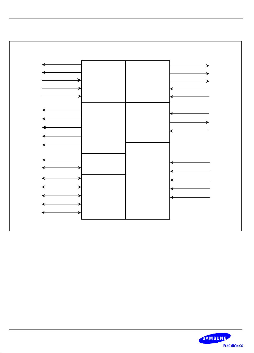
Figure2-1 shows the 44 external signals for the 10/100 Mbit/s Ethernet Physical Layer Transceiver, divided into
functional groups. Power and ground pins need to be added to this signal list. The device will require a 64 pin
package. This chapter groups the signal definitions by functional area, giving each signal’s symbolic name, full
name, type, and a brief definition. The groups are:
• pins for MII Transmit
• pins for MII Receive
• pins for MII Station Management
• pins for Twisted-Pair Interface
• pins for Analog Pins
• pins for LED Indicators
• pins for Control Signals
2-1
Page 15
Preliminary Spec. ver 1.4
EXTERNAL SIGNALS KS8910 100/10 Mbps ETHERNET TRANSCEIVER
EXTERNAL SIGNALS
Col
Tx_clk
TxD[3:0]
Tx_en
Tx_er
CrS
Rx_clk
RxD[3:0]
Rx_DV
Rx_er
MDC
MDIO
LEDC
LEDL
LEDT
LEDR
Transmit
Media
Independent
Interface(MII)
Receive
Media
Independent
Interface(MII)
MII
Management
LED
Interface
Twisted
Pair
Interface
Analog Pins
Controls
TPOP
TPON
TPOB
TPIP
TPIN
XTAL_IN
XTAL_OUT
RB
AN_EN
SP_SEL
FDUPL
PD
RESET
2-2
LEDS
Figure 2-1. External Signals
Page 16
Preliminary Spec. ver 1.4
LEDC[ID4]
LEDL[ID3]
LEDT[ID2]
LEDR[ID1]
LEDS[ID0]
XTAL_OUT
KS8910 100/10 Mbps ETHERNET TRANSCEIVER EXTERNAL SIGNALS
PIN ASSIGNMENTS
VSSDIG
VDDDIG
RxD0
RxD1
RxD2
RxD3
MDC
MDIO
VSSIO
VDDIO
VSSRXA
VDDRXAPDVSSRXQ
VDDRXQ
RESET
Rx_DV
Rx_clk
Rx_er
Tx_er
Tx_clk
SUBDIG
SUBIO
VSSIO
VDDIO
Tx_en
TxD0
TxD1
TxD2
TxD3
Col
CrS
484746454443424140393837363534
49
50
51
52
53
54
55
56
57
58
59
60
61
62
63
64
123456789
VSSDIG
VDDDIG
KS8910
64QFP-1414
Top View
VSSIO
FDPLX
33
10111213141516
VDDIO
VSSTXA
XTAL_IN
VDDTXA
VSSTXQ
VDDTXQ
32
31
30
29
28
27
26
25
24
23
22
21
20
19
18
17
TPIP
TPIN
SUBANA
SP_SEL
VDDREF
VSSREF
RB
RBGND
AN_EN
TPON
VSSDRV
TPOP
SUBDRV
TPOB
VDDDRV
VSSDRV
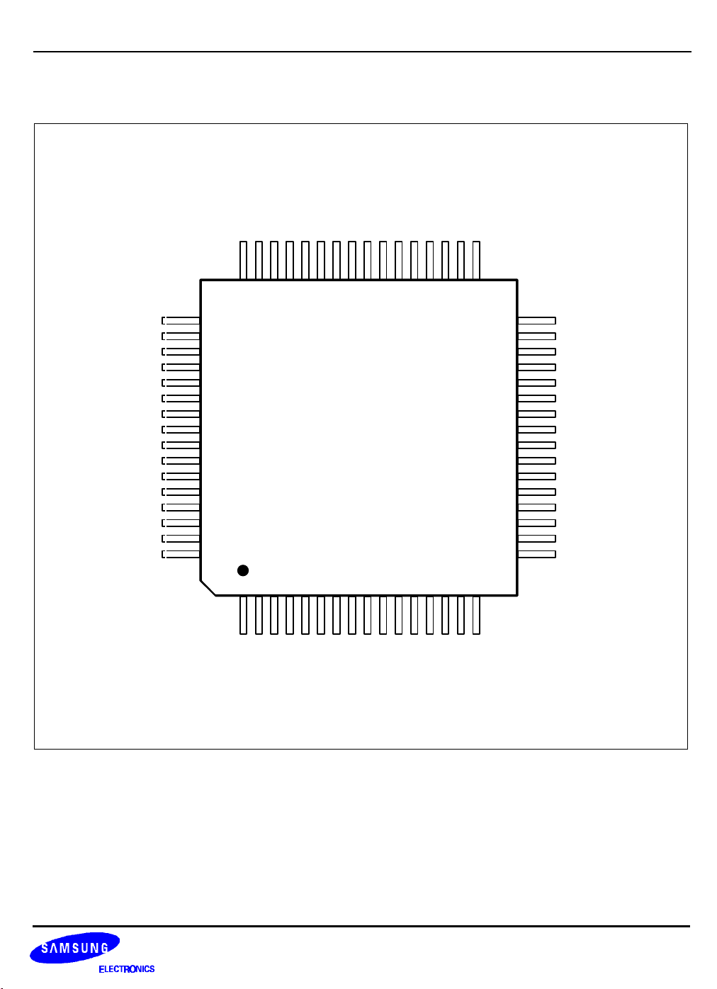
Figure 2-2. KS8910 Pin Assignments
2-3
Page 17

Preliminary Spec. ver 1.4
EXTERNAL SIGNALS KS8910 100/10 Mbps ETHERNET TRANSCEIVER
SIGNAL DESCRIPTIONS
Table 2-1. KS8910 Signal Descriptions
Signal Pin Number I/O Description
MEDIA INDEPENDENT INTERFACE (MII) SIGNALS
The MII is the interface between the 10/100 Mbit/s Ethernet Transceiver and a Media Access Control (MAC)
device. MII is a nibble-wide interface clocked at either 2.5MHz or 25MHz. The Transceiver side MII interface
supplies both the transmit and receive clocks.
Transmit MII Signals
The next sub-table shows the MII signals supported by the 10/100Mbit/s Ethernet Transceiver for transmitting
data packets. For a detailed description of these signals, see the MII sections of the IEEE 802.3u documents listed
in the reference document section
Col 63 O
Tx_clk 53 O
TxD[3:0] 62,61,60,59 I
Collision :
5T
Asserted asynchronously with minimum delay from the start of a collision
on the medium.
t/s
Transmit clock :
5T
TxD[3:0] and Tx_en are driven off the rising edge of the Tx_clk by the
MAC, and sampled by the Transceiver on the rising edge of the Tx_clk.
t/s
Transmit data :
5T
Transmit data is aligned on nibble boundaries. TxD[0] corresponds to the
first bit to transmit on the physical medium and is the LSB of the first byte,
PD
followed by the fifth bit of that byte during the next clock.
Tx_en 58 I
Tx_er 52 I
Transmit enable :
Tx_en provides precise framing for the data carried on TxD[3:0]. It is active
5T
during the clock periods that TxD[3:0] contains valid data to be transmitted,
PD
from preamble through CRC.
Transmit coding error :
Tx_er is driven synchronously to Tx_clk and is sampled continuously by
5T
the Transceiver. If asserted for one or more Tx_clk periods, it causes the
PD
Transceiver to emit one or more symbols which are not part of the valid
data or delimiter set somewhere in the frame being transmitted.
Receive MII Signals
The next sub-table shows the MII signals supported by the 10/100Mbit/s Ethernet Transceiver for receiving data
RX_CLK packets. For a detailed description of these signals, see the MII sections of the IEEE 802.3u standard
listed in the reference document section.
CrS 64 O
2-4
Carrier sense :
Asserted asynchronously with minimum delay from the detection of a non-
5T
idle medium.
t/s
Page 18

Preliminary Spec. ver 1.4
KS8910 100/10 Mbps ETHERNET TRANSCEIVER EXTERNAL SIGNALS
Table 2-1. KS8910 Signal Descriptions
Signal Pin Number I/O Description
Rx_clk 50 O
Receive clock :
5T
Rx_clk is a continuous clock. In 4-bit mode, its frequency is 25 MHz for
t/s
100Mbit/s operation, and 2.5 MHz for 10Mbit/s. RXD[3:0], Rx_DV, and
Rx_er are driven by the Transceiver off the falling edge of Rx_clk, and
sampled on the rising edge of Rx_clk.
RxD[3:0] 46,45,44,43 O
Receive data :
5T
RxD is aligned on nibble boundaries. RxD[0] corresponds to the first bit
t/s
received on the physical medium which is the LSB of the byte in one clock
period and the fifth bit of that byte in the next clock.
Rx_DV 49 O
Receive data valid :
5T
PHY asserts Rx_DV synchronously and holds it active during the clock
t/s
periods that RxD[3:0] contains valid received data. The Transceiver
asserts Rx_DV no later than the clock period when it places the first
nibble of the start frame delimiter (SFD) on RxD[3:0]. If the Transceiver
asserts Rx_DV prior to the first nibble of the SFD, then RxD[3:0] carries
valid preamble symbols.
O
Rx_er 51
Receive error :
5T
PHY asserts Rx_er synchronously whenever it detects a physical medium
t/s
error, e.g., a coding violation. The Transceiver asserts Rx_er only when it
asserts Rx_DV.
MII Station Management Signals
The next sub-table shows the two MII station management signals. Use of these signals for configuring the
transceiver or negotiating a link protocol is optional.
MDC 42
I
Management Data Clock :
5T
The timing reference for transfer of information on the MDIO signal. With
PD
the PCI clock at 33 MHz, the MDC clock has a maximum clock frequency
of 33/14 = 2.36 MHz. The minimum clock period is 424 ns.
I/O
MDIO 41
Management Data I/O :
5T
MDIO transfers control and status management data from the attached
t/s
MAC. MDIO Transmits status information from the PHY to the MAC.
PD
LED INTERFACE
These signals allow connection of LEDs to monitor the status of the Transceiver. The next sub-table shows a
summary of the LED signals generated by the Transceiver.
LEDC[D4] 3
Collision Indicator /Device ID4:
Pulled low for 10ms when a collision is detected. Otherwise LEDC is high
I/O
LEDL[D3] 4 Link Integrity Indicator /Device ID3:
5T
t/s
Pulled low during link test pass
LEDT[D2] 5 Transmit Indicator /Device ID2:
2-5
Page 19

Preliminary Spec. ver 1.4
EXTERNAL SIGNALS KS8910 100/10 Mbps ETHERNET TRANSCEIVER
Table 2-1. KS8910 Signal Descriptions
Signal Pin Number I/O Description
LEDR[D1] 6
Receive Indicator /Device ID1:
I/O
LEDS[D0] 7 Speed Indicator /Device ID0:
5T
Pulled low when 100Mbit/s operation is in affect either by manual
t/s
selection or after Arbitration. Pulled high when 10Mbit/s operation is in
affect and during Auto-Negotiation.
ANALOG PINS
The next sub-table shows the signals needed to support the analog circuitry in the Transceiver.
XTAL_OUT 11 O Oscillator Input/Output :
A ±50ppm 25 MHz oscillator is connected between these two pins. This
oscillator is used to time the 10Mbit/s transmitter and as a reference for the
XTAL_IN 12 I
clock recovery of both the 10Mbit/s and 100Mbit/s serial data. A frequency
synthesizer uses this crystal reference to produce the 100Mbit/s transmit
clock(125MHz).
TWISTED PAIR INTERFACE
The next sub-table lists the signals used to send and receive 100Mbit/s data on twisted pairs.
TPOP 21
TPON 23
TPIP 32
TPIN 31
O TPOP/TPON :
Differential driver outputs to the cable magnetics. The on-chip driver circuit
O
automatically switches between 10Mbit/s and 100Mbit/s operation.
I TPIP/TPIN :
Differential receiver inputs from the cable magnetics.
I
TPOB 19
O Provides a bias for the transmit transformer center tap. This bias is about
2.6 volts and should be connected with the Capacitor on GND.
CONTROL SIGNALS
The next sub-table shows the control signals. These control signals select various modes of operation of the
Transceiver
AN_EN
24 5T
Enables autonegotiation of operation speed.
PU
SP_SEL
29 100/10 Mbit/s is sampled at the negation of the RESET signal. A high level
on this input selects 100Mbit/s operation. A low level selects 10Mbit/s.
When undriven, this input will float high setting the default operation to
100Mbit/s.
RESET
33 Master reset for the Transceiver. Resets all digital logic and some analog
circuits.This Reset is an active Low.
PD 36
5T
Power Down Mode
PD
FDPLX 8
2-6
Enables full duplex operation.
Page 20

Preliminary Spec. ver 1.4
KS8910 100/10 Mbps ETHERNET TRANSCEIVER EXTERNAL SIGNALS
Table 2-1. KS8910 Signal Descriptions
Signal Pin Number I/O Description
Power and Ground Signals
VDDDIG 2,47
VDDIO 10,39,57
VDDTXA 14
VDDRXA 37
VDDREF 28
VDDTXQ 16
VDDRXQ 34
VDDDRV 18
VSSDIG 1,48
VSSIO 9,40,56
VSSTXA 13
VSSRXA 38
VSSREF 27
VSSTXQ 15
VSSRXQ 35
P
3.3V Power Supply for Digital Internal Block
P
3.3V Power Supply for Digital I/O Block
P
3.3V Power Supply for Analog Block
P
3.3V Power Supply for Analog Block
P
3.3V Power Supply for Analog Reference Block
P
3.3V Power Supply for Analog Block
P
3.3V Power Supply for Analog Block
P
3.3V Power Supply for Analog Driver Block
G
Ground for Digital Internal Block
G
Ground for for Digital I/O Block
G
Ground for for Analog Block
G
Ground for for Analog Block
G
Ground for for Analog Reference Block
G
Ground for for Analog Block
G
Ground for for Analog Blcok
VSSDRV 17,22
SUBIO 55
SUBDIG 54
SUBANA 30
SUBDRV 20
RBGND 25
G
Ground for for Analog Driver Block
G
Bulk Ground for Digital I/O Block
G
Bulk Ground for Digital Internal Block
G
Bulk Ground for Analog Block
G
Bulk Ground for Analog Driver Block
G
Reference Ground
RB 26 Reference Bias Resistor
NOTES:
1.t/s: (sustained)tri-state, 5T: 5V Tolerance,
2.PD: Pull Down, PU: Pull Up
3.P: Power Supply
4.G: Ground
2-7
Page 21

Preliminary Spec. ver 1.4
EXTERNAL SIGNALS KS8910 100/10 Mbps ETHERNET TRANSCEIVER
MEMO
2-8
Page 22
Preliminary Spec. ver 1.4
KS8910 100/10 Mbps ETHERNET TRANSCEIVER FINCTIONAL BLOCKS
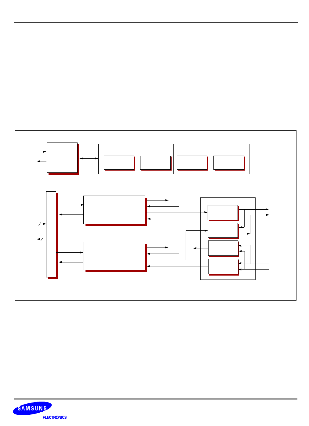
3 FUNCTIONAL BLOCKS
This section of the specification provides a description of the functional blocks of the KS8910 10/100 Mbit/s
Ethernet Transceiver architecture. The next Chapter of the document will describe the blocks in detail. Shown in
Figure3-1 are the functional blocks in the architecture.
MDC
MDIO
4
TX
4
RX
MI
Station
MGM
Interface
Mll Data Interface
Control
Registers
10/20MHz
10 Base-T
25MHz/125MHz
Fast Ethernet
100 Base-TX
Registers
20MHz
Status
Registers
Link Status
Auto-Negotiation
Power
Management
Link Control
Figure 3-1. Functional Block Diagram of KS8910
Auto-neg
Arbitration
Driver
MLT3
Driver
10RX
100RX
20MHz
TX
RX
+
-
+
-
MII DATA INTERFACE
The purpose of the MII data interface is to provide a simple, inexpensive, and easily implemented interconnection
between the Media Access Control (MAC) sublayer and Physical (PHY) layer devices and between PHY layer
devices and Station Management. The MII interface provides a uniform interface to the Reconciliation Sublayer for
all 100Base-T physical layer device implementation. Services required by the MII include the following:
3-1
Page 23

Preliminary Spec. ver 1.4
FUNCTIONAL BLOCKS KS8910 100/10 Mbps ETHERNET TRANSCEIVER
• Mapping of transmit and receive code-bits between the PMA’s client and the underlying PMD,
• Generating a control signal indicating the availability of the PMD to a PCS or other client and synchronizing
with Auto-Negotiation
• Encoding (decoding) of MII data nibbles to (from) 5-bit code-groups (4B/5B)
• Generating Carrier Sense and Collision Detect indications
• Serialization (deserialization) of code-groups for transmission (reception) on the underlying serial PMA.
• Mapping of Transmit, Receive, Carrier Sense and Collision Detection between the MII and the underlying PMA.
MANAGEMENT AGENT
A management interface having dedicated registers used to communicate Auto-Negotiation information to the MII
that includes the control, status, advertisement, link partner ability, and expansion registers.
POWER MANAGEMENT
Power management is performed on the transceiver by monitoring data stream activity and powering down
segments of the chip to conserve power. The power-down modes selected are based on maximizing power
conservation on-board the Transceiver chip.
Auto Power Down Function(10/100Mbps)
CONTROL REGISTERS / STATUS REGISTERS
The control and status registers set are used to control and monitor the 10Base-T/100Base-TX Transceiver chip
and can be accessed through the MII management interface. The management interface consists of a pair of
signals which physically transport the management information across the MII, a frame format and a protocol
specification for exchanging management frames, and a register set which can be read and written using these
frames. The register definition specifies a basic register set with a extension mechanism.
AUTO-NEGOTIATION
The Auto-negotiation provides a mechanism to control connection of a single MDI to a single PMA type, where
more than one PMA type may exist. Management may provide additional control of Auto-negotiation through the
management function, but the presence of a management agent is not required.
The Auto-negotiation function provides the Auto-Negotiation Transmit, Receive, Arbitration, and Normal Link
Pulses (NLP) receive link integrity test functions. The Auto-negotiation functions interact with technology
dependent PMA’s through the technology dependent interface. The Technology dependent interface includes
10Base-T/100Base-TX and 100Base-T4.The KS8910 does not support 100Base-T4.
3-2
Page 24
Preliminary Spec. ver 1.4
KS8910 100/10 Mbps ETHERNET TRANSCEIVER FINCTIONAL BLOCKS
100 BASE-TX DIGITAL BLOCK
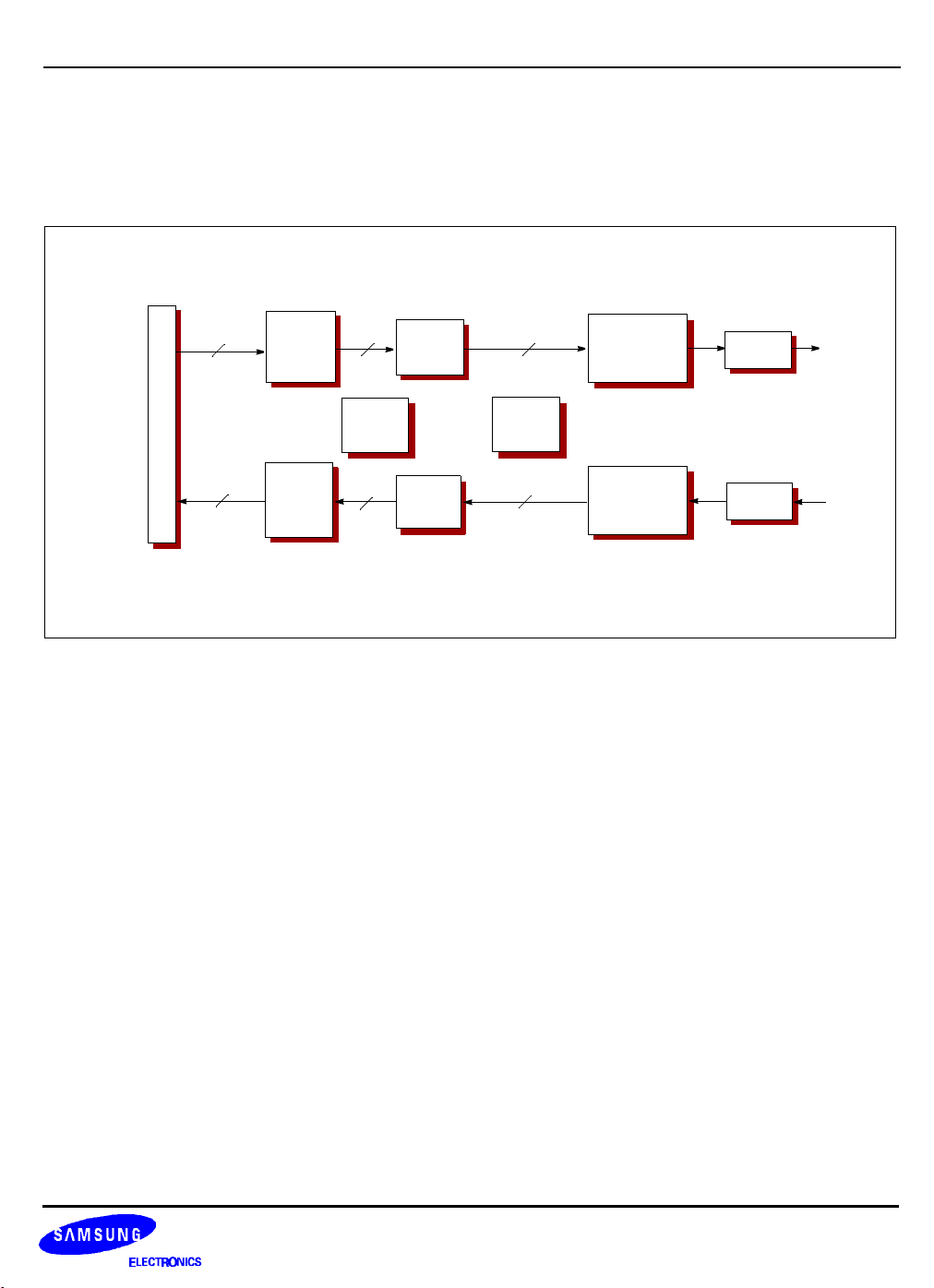
A functional description of the 100Base-TX digital blocks in the 10/100 Mbit/s Transceiver is provided in this
section. Shown in Figure 3-2 is the functional blocks of 100Base-TX digital architecture.
4
M
I
I
4
4B/5B
5B/4B
5
P
¡
S
Carrier
Sense
5 1
P
¡
S
1
Link
Monitor
Serial
Scrambler
Serial
DeScrambler
NRZI
NRZ
Figure 3-2. 100Base-TX Digital Bolck of KS8910
4B/5B
The symbol encoder converts 4-bit (4B) nibble data generated by the MAC into 5-bit (5B) symbols for transmission.
This conversion is required to allow control symbols to be combined with data symbols.
The symbol encoder substitutes the first 8 bits of the MAC preamble with a J/K symbol pair (11000 10001). The
symbol encoder continues to replace subsequent 4B codes with corresponding 5B symbols. At the end of the
transmit data packet, the symbol encoder injects the T/R symbol pair indicating end of frame.
The symbol encoder continuously injects IDLE symbols into the transmit data stream until the next transmit data
packet is detected.
Parallel to Serial Block
The Parallel to Serial Block performs Serialization of code-groups for transmission on the underlying serial Physical
Medium attachment sublayer.
NRZI to NRZ Block
The NRZI to NRZ Block formats NRZI data to NRZ format for descrambling. With the receive data in NRZ format,
the descrambler can properly synchronize with the scrambled data.
3-3
Page 25

Preliminary Spec. ver 1.4
FUNCTIONAL BLOCKS KS8910 100/10 Mbps ETHERNET TRANSCEIVER
Serial Scrambler
The Serial Scrambler is used to minimize electromagnetic emissions from the TP-PMD physical link. Serial
Scrambling randomizes the data spectrum by the addition of a pseudo-random key sequence to the plain-text
sequence transmitted by the PHY. The length of the pseudo-random sequence is chosen to reduce radiated
emissions by approximately 20 dB when the station is transmitting the Idle Line State. This radiation reduction is
necessary in order to meet regulatory requirements in many countries.The Serial Scrambler also has the desirable
property that single bit errors in the received scramble serial stream decode as single bit errors in the recovered
plain-text stream.
Serial Descrambler
In the Serial Descrambler the pseudo-random sequence is subtracted by the receiver to recover the transmitted
data.
NRZ to NRZI Block
This block receives scrambled transmit data stream and NRZI encodes the data in order to comply with the TPPMD standard for 100Base-TX transmission over Category-5 unshielded twisted pair cable.
Serial to Parallel Block
The function of the Serial to Parallel block is to provide Serial to Parallel conversion of code-groups for reception
from the underlying Physical Medium attachment sublayer.
5B/4B
The 5B/4B functional block Maps 5-bit nibbles from the PCS into 4-bit code groups.
Link Monitor Block
The link monitor is responsible for determining whether the underlying receive channel is providing reliable data.
Failure of the underlying channel typically causes the PMA’s client to suspend normal operation. The Link Monitor
function takes advantage of the PMD sublayer’s continuously-signaled transmission scheme, which provides the
PMA with a continuous indication of signal detection on the channel through signal_status as communicated by a
signal from the PMD. It responds to control by Auto-Negotiation, when implemented, which is effected through the
link control parameter of PMA_SIGNAL request.
Loop-Back Function
Digital side
3-4
Page 26
Preliminary Spec. ver 1.4
KS8910 100/10 Mbps ETHERNET TRANSCEIVER FINCTIONAL BLOCKS
10BASE-T DIGITAL BLOCK
The 10BASE-T digital block interfaces a back-end controller to a twisted-pair (TP) cable. The controller interface
includes transmit and receive clock and Manchester data as well as mode control logic and signaling. And the
10BASE-T Transceiver has synthesized clocks derived from a 25 MHz crystal oscillator and five LED drivers for
visual status reporting.
The 10BASE-T Transmit function refers to data transmitted to the twisted-pair network.The Receive function refers
to data received by the back end from the twisted-pair network. In the integrated PLS/MAU mode, the 10BASE-T
Ethernet Interface performs all required MAU functions defined by the IEEE 802.3 10BASE-T specification such as
collision detection, link integrity testing, signal quality error messaging, jabber control and loopback.
The 10Base-T digital block also provides repeater clients an indication that a carrier event has been sensed and an
indication if it is deemed in error. A carrier event is defined as receipt of two non-contiguous ZEROS within any l0
rx_code-bits. A carrier event is in error if it does not start with a Start-of-Stream Delimiter.
10Base-T Digital Block Diagram
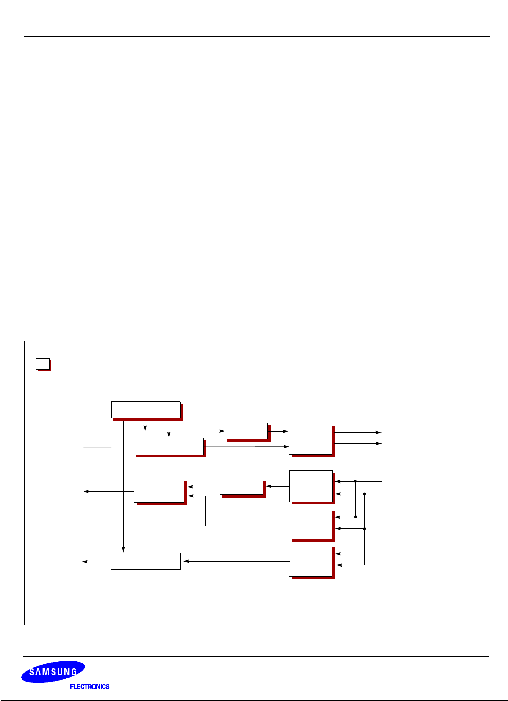
100BASE-TX AND 10BASE-T ANALOG BLOCKS
Figure3-3 shows the Analog Blocks of KS8910 10/100 Mbit/s Ethernet Transceiver.
10Mbit/s Analog Block
TXPLL
100M
10M
100M
10M
WAVE SHAPER
RXPLL
DPLL
MLT-3
BW EQ
DRIVER
100M
RX EQ
SD
10M
RX SQ
TPOP
TPON
TPIP
TPIN
Figure 3-3. Analog Blocks of KS8910
3-5
Page 27

Preliminary Spec. ver 1.4
FUNCTIONAL BLOCKS KS8910 100/10 Mbps ETHERNET TRANSCEIVER
Transmit Clock (TXPLL)
Internal clock synthesizer serves as internal master clock distribution system supplying all transmit clock reference.
The transmit clock block includes crystal oscillator, PLL frequency synthesis, and frequency divider functions
needed to generate all of the transmit clocks used in the design from a 25 MHz crystal attached to the chip. This
block generates 2.5 MHz, 10 MHz, 20 MHz, 25 MHz and 125 MHz clocks. The transmit frequency synthesizer
circuit uses an on-chip VCO.
Encoder (MLT-3)
The NRZI to MLT-3 Encoder receives the scrambled NRZI data stream from the PMA and encodes it into MLT-3 for
presentation to the Twisted-Pair Transmit Driver. MLT-3 coding has certain similtarities to NRZI, but three levels are
output instead of two, i.e. Positive voltage, Zero voltage and Negative voltage. A MLT-3 coded data stream keeps
cycling from Positive voltage to Zero voltage to Negative voltage and back to Positive voltage through Zero Voltage.
Each time a logic “1” is encoded a transition will take place. Each time a logic “0” is encoded the previous output
level will be maintained for another bit period.
Receive and Baseline Wander Equalization (RX EQ/BW EQ)
The receive equalizer compensates for amplitude and phase variations introduced by twisted pair cable. The
equalizer compensates the transfer functions of cables over the range of 0 meters to 100 meters.The equalization
circuit also corrects for baseline wander that is introduced by AC coupling transformers. The equalization circuits
require no off-chip components or external adjustments.
Signal Dectector
The Signal Detector monitors signal amplitude on cable and inform Digital Block about existence of 100
Rx_code_bit by checking link_status. Threshold of Detect Assertion is 400mVp-p and Detect Deassertion is
300mVp-p.
Receive Timing Recovery
The receive timing recovery circuit generates a 125 MHz clock and re-timed data from the equalized signal. The
timing recovery circuit uses an on-chip VCO.
Receive Squelch (RX SQ)
Receive squelch circuitry serves as receive signal slicer and noise rejector. The receive squelch circuit is activated
if the input signal amplitude is decreased below the carrier detect deassertion threshold of 300 mV peak-to-peak.
This prevents the transmission of high bit error rate data to the digital and protocol sections of the chip.
LED DRIVER
The KS8910 supports five status LEDs and LED pins are shared with PHY address.These pins can be externally
strapped as ‘High’ or ‘Low’ to encode different PHY addresses. When the pin is strapped to Low, the associated
LED will be actived to ‘High’. When the pin is strapped to ‘High’,the associated LED will be actived to ‘Low’
3-6
Page 28

Preliminary Spec. ver 1.4
KS8910 100/10 Mbps ETHERNET TRANSCEIVER 100BASE-TX DIGITAL BLOCKS
4 100 BASE-TX DIGITAL BLOCKS
OVERVIEW
This chapter describes the physical coding sublayer (PCS), physical medium attachment (PMA) sublayer, and the
physical medium dependent sublayer (PMD) for comprehension of the 100Base-TX within the KS8910.
This is based upon the IEEE 802.3U/D5.3 specification and ANSI X3.263:1995 TP-PMD, Revision 2.2 (1March
1995) specification.
PHYSICAL CODING SUBLAYER (PCS)
The PCS interface is the Media Independent Interface (MII) which provides a uniform interface to the Reconciliation
Sublayer for 100Base-TX of the KS8910.
The KS8910’s PCS realizes the following functions:
• Encoding (decoding) of MII data nibbles to (from) 5-bit code-groups (4B/5B)
• Generating Carrier Sense and Collision Detect indications
• Serialization (deserialization) of code-groups for transmission (reception) on the underlaying serial PMA
• Mapping of Transmit, Receive, Carrier Sense and Collision Detection between the MII and the underlying PMA
4-1
Page 29

Preliminary Spec. ver 1.4
100BASE-TX DIGITAL BLOCKS KS8910 100/10 Mbps ETHERNET TRANSCEIVER
PHYSICAL MEDIUM ATTACHMENT SUBLAYER (PMA)
The PMA provides a medium-independent means for the PCS and other bit-oriented clients to support the use of a
range of physical media. The KS8910’s PMA performs the following functions:
• Mapping of transmit and receive code-bits between the PMA’s client and the underlying PMD
• Generating a control signal indicating the availability of the PMD to a PCS or other client and synchronizing
with Auto-Negotiation
• Scrambling and descrambling of the transmit code-bits and the receive code-bits, respectively.
• Conversion of the scrambled transmit code-bits from NRZ to NRZI and reverse for the receive code-bits.
PHYSICAL MEDIUM DEPENDENT SUBLAYER (PMD)
The KS8910’s PMD receives NRZI code-bits from the PMA, encodes them into MLT-3, and transmits them to the
adjacent PMD over the physical link. The PMD also decodes the incoming bits and delivers them to the PMA in
NRZI format. Furthermore, the PMD recovers the clock from the incoming data bits. The PMD block is an Analog
Block.
DESCRIPTION OF OPERATION
Transmit operation
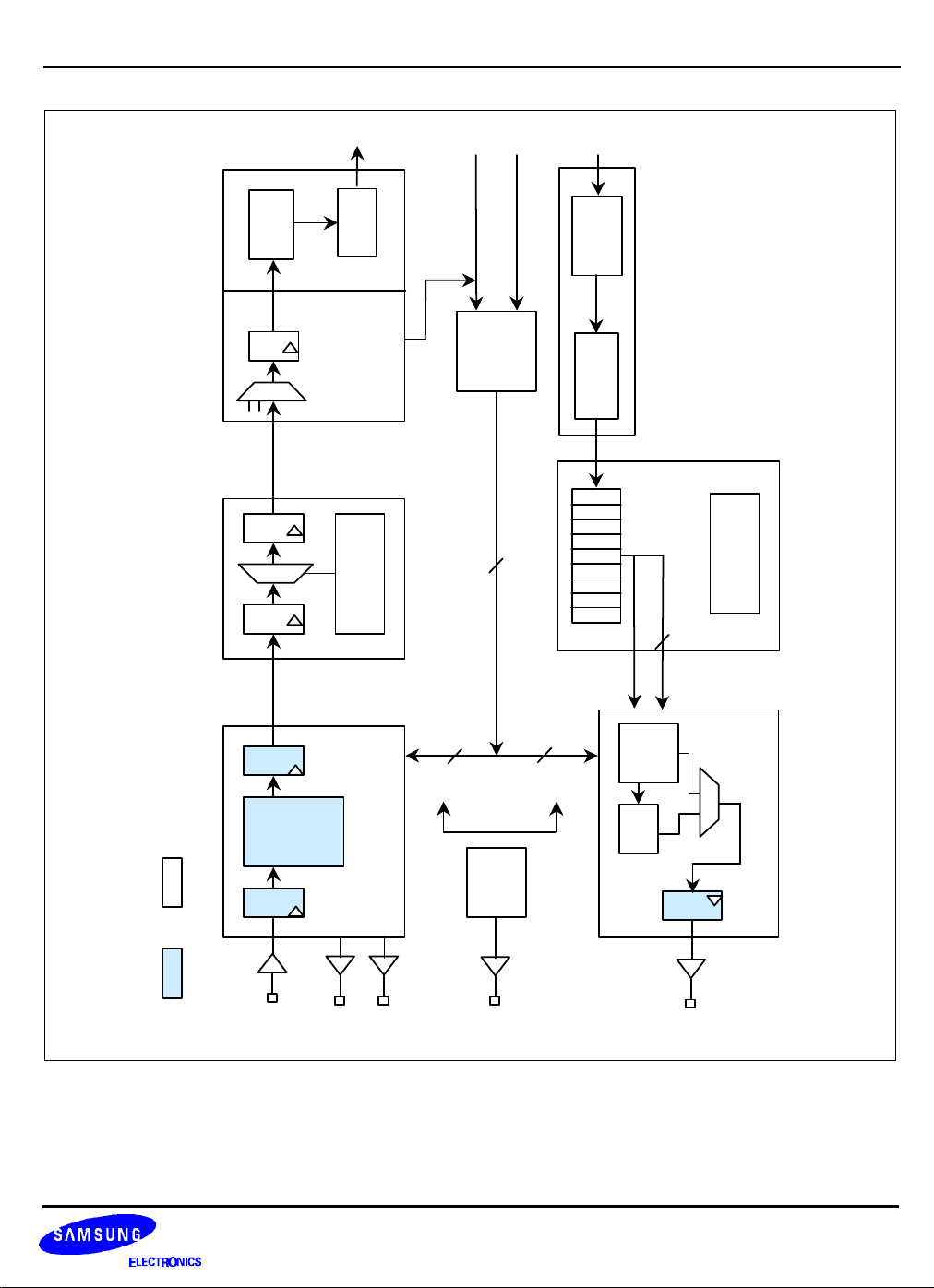
Data for transmission is received in nibbles by the PCS over the MII. The PCS then converts each nibble into a 5bit code-group which is serialized and forwarded to the PMA. The PMA scrambles the serialized bit stream and
converts it from NRZ to NRZI before it is forwarded to the PMD.The PMD converts the NRZI formatted outgoing bit
stream into MLT-3.
The first half of the above described data flow is illustrated in the Figure 4-1.
Receive operation
The incoming bit stream transmitted by the remote PMD through the physical link is received in MLT-3 format. The
PMD converts it into an NRZI formatted bit stream and then recovers the clock as well as data. The data stream is
changed into NRZ format by the PMA which also descrambles it. The PCS then looks for a Start-of-Stream Delimit,
SSD, in the incoming data stream, locks to it and converts it into 5-bit code-groups in parallel format. Each codegroup is, thereupon, translated into it’s corresponding 4-bit group and transmitted nibblewise over the MII which is
partly shown in Figure4-1.
4-2
Page 30
Preliminary Spec. ver 1.4
RX_EROUT
RX_CLKOUT
_RXBITSSM
KS8910 100/10 Mbps ETHERNET TRANSCEIVER 100BASE-TX DIGITAL BLOCKS
125MHz
Scrambler
0
1
PCS_TRANSMIT_BITS PMA_TXPCS_TRANSMIT
5
4B/5B
Encoder
TX_CODE_BIT
TX_BIT[4:0]
State
Machine
NRZI
PCS_TXBITSSM
SIGNAL_STATUS
LINK_CONTROL[1:0]
PMA_LMSM
LINK
2
LINK_STATUS[1:0]
2
TRANSMITTING
1/
MONITOR
PMA_RX
9 0
PCS_RECEIVE_BITS
2
PMA_RXSM
NRZI¡ NRZ
Descrambler
RECEIVING
1/
Receive
10
4B/5B
got_code
10
State
Machine
Decoder
PCS
RX_BIT[9:0]
4
4
4
PCS_CARSM
CARRIER
SENSE
25MHz
6 4
TX_EN
TX_ER
TX_CLKOUT
COL OUT
OUTPUT
TXD[3:0]
PCS_RECEIVE
Figure 4-1. 100Base-TX Operational Block Diagram of KS8910
7
RX_DOUT[3:0]
RX_DVOUT
4-3
Page 31
Preliminary Spec. ver 1.4
100BASE-TX DIGITAL BLOCKS KS8910 100/10 Mbps ETHERNET TRANSCEIVER
PHYSICAL CODING SUBLAYER (PCS)
The KS8910 PCS maps data and control signals between the MII and PMA. The PCS consists of five functional
blocks as it appears in Figure4-2.
MII
PMA
TxD[3:0]
Tx_en
Tx_er
PCS
TXbits[4:0]
TXbits_en
4B/5B
Encoder
Serial
Converter
TX_code-bit
Tx_clk
Col
Transmitting Receiving
CrS
Carrier
Sense
Link_status[1:0] RX_code-bit
RxD[3:0]
Rx_DV
Rx_er
Rx_clk
5B/4B
Decoder
Parallel
Converter
RXbits[9:0]
RXbits_en
25Mhz
Domain
125Mhz
Domain
Figure 4-2. PCS Functional Block Diagram of KS8910
In the transmit direction the PCS encodes the data nibbles, received through the MII, into 5-bit code-groups. The
data is, thereupon, serialized and forwarded to the PMA.
In the receive direction data is first deserialized into 5-bit code-groups. This requires that the Parallel Converter has
been able to lock to the incoming data stream which is the case after reception of Start-of-Stream Delimiter, SSD.
The 5-bit code-groups are then decoded into data nibbles which are transferred to the MAC through the MII.
Because of the different wire bit rates of data in parallel form and serial form, two different clocks are required. The
encoding takes place in the 25 MHz clock domain while all other functions require a 125 MHz clock.
A detailed description of each functional block is given the following sub-sections.
4B/5B ENCODER, DECODER
The mapping of the data nibbles into 5-bit code-groups and vice versa is done according to table 24-1 in the IEEE
802-3u standard. Shown at 4B/5B Coding table 4-1 of KS8910.
4-4
Page 32

Preliminary Spec. ver 1.4
KS8910 100/10 Mbps ETHERNET TRANSCEIVER 100BASE-TX DIGITAL BLOCKS
Table 4-1. 4B/5B Coding of KS8910
Code Type
4B Code
[3:0]
Name
5B Symbol
[4:0]
Interpretation
0000 0 11110 “0” Data
0001 1 01001 “1” Data
0010 2 10100 “2” Data
0011 3 10101 “3” Data
0100 4 01010 “4” Data
0101 5 01011 “5” Data
0110 6 01110 “6” Data
DATA
0111 7 01111 “7” Data
1000 8 10010 “8” Data
1001 9 10011 “9” Data
1010 A 10110 “A” Data
1011 B 10111 “B” Data
1100 C 11010 “C” Data
1101 D 11011 “D” Data
1110 E 11100 “E” Data
1111 F 11101 “F” Data
IDLE Undefined I 11111 Idle. Used as inter-steam fill code
0101 J 10001 First symbol of Start-of-Stream Delimiter(SSD1)
CONTROL
0101 K 01101 Last symbol of Start-of-Stream Delimiter(SSD2)
undefined T 00111 First symbol of End-of-Stream Delimiter(ESD1)
undefined R 00111 Last symbol of End-of-Stream Delimiter(ESD2)
undefined H 00100 Transmit Error:used to force signal error
undefined Invalid 00000 Invalid
undefined Invalid 00001 Invalid
undefined Invalid 00010 Invalid
undefined Invalid 00011 Invalid
INVALID
undefined Invalid 00101 Invalid
undefined Invalid 00110 Invalid
undefined Invalid 01000 Invalid
undefined Invalid 01100 Invalid
undefined Invalid 10000 Invalid
undefined Invalid 11001 Invalid
4-5
Page 33

Preliminary Spec. ver 1.4
100BASE-TX DIGITAL BLOCKS KS8910 100/10 Mbps ETHERNET TRANSCEIVER
4B/5B ENCODER (TRANSMIT STM)
The 4B/5B Encoder converts the received data nibbles into 5-bit code groups. This is a trivial translation process
except for the first two nibbles of the preamble which are substituted by the Start-of-Stream Delimiter, SSD.
Likewise, an End-of-Stream Delimiter, ESD, is added to the end of the transmitted data packet. The data packet is
fully recovered by the receiving 5B/4B decoder, i.e. the ESD is stripped and the SSD is changed back to the
preamble bit pattern.
The collision signal, COL, is put into the active state when transmission and reception are detected at the same
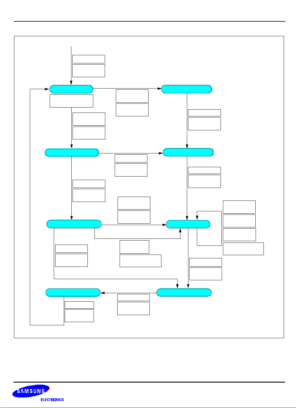
time. The 4B/5B Encoder is implemented as a state machine. The state diagram is given in Figure4-3. The state
“ERROR CHECK” of the state machine given in Figure 24-8 in the IEEE 802.3u standard has been merged into the
states “TRANSMIT” and “END STREAM T” for better efficiency.
4B/5B DECODER(RECEIVE STM)
The 5B/4B Decoder converts the received 5-bit code-groups into nibbles. In general, this is a trivial translation
process. However, preamble bits have to be substituted for the first two code-groups of a packet, the Start-ofFrame Delimiter. The 5B/4B Decoder scans the incoming bit stream for the SSD and locks to it. After locking to the
incoming bit stream each 5-bit code group is translated into a nibble according to table 24-1 in the IEEE 802.3u
standard. The last two code-groups of a packet, which is the End-of-Stream Delimiter, are removed from the code
stream.
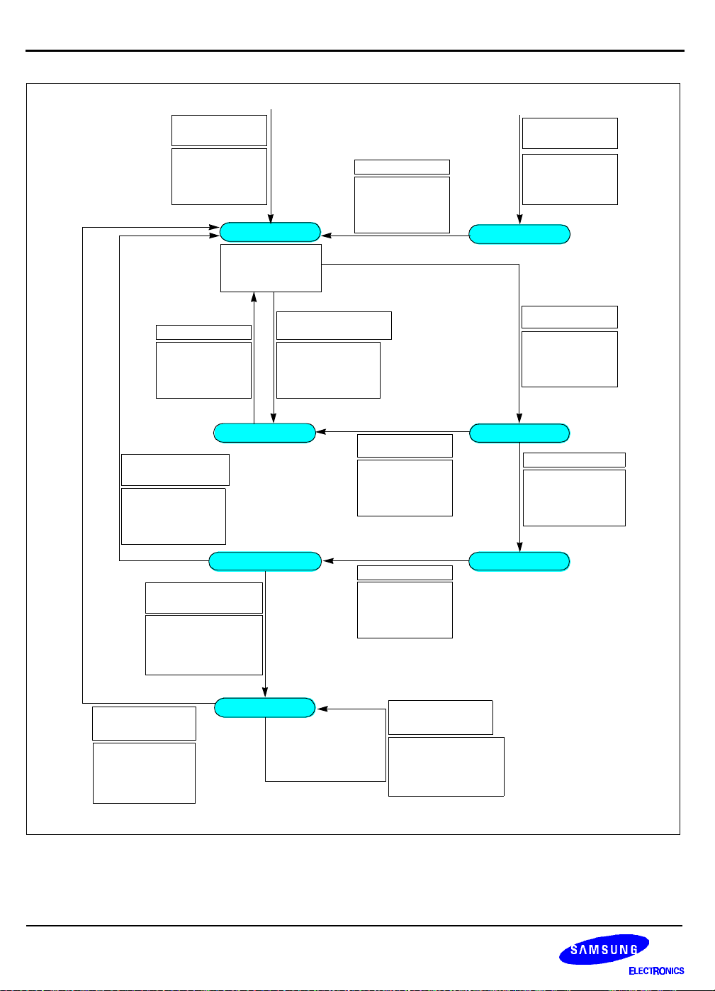
The states “CARRIER DETECT,” “CONFIRM K,” “START OF STREAM J” and “START OF STREAM K” in figure
24-11 in the IEEE 802.3u standard have been combined into “CONFIRM J” and “CONFIRM K” for better efficiency.
The same is true for “RECEIVE,” “DATA,” “DATA ERROR,” “PREMATURE END” and “END OF STREAM” which
have been merged into the “DECODE” state.
In the “DECODE” and “START STREAM” states, the outputs’ values depend on the received bit stream. The
relationship appears in Table4-2.
The 5B/4B decoder is implemented as a state machine with the state diagram shown in Figure4-4.
Table 4-2. 5B/4B Outputs
OUTPUT 0 1
Rx_DV {esd1, esd2} else
Rx_er valid data / {esd1, esd2} else
init_RXbits else {esd1, esd2}
4-6
Page 34
Preliminary Spec. ver 1.4
KS8910 100/10 Mbps ETHERNET TRANSCEIVER 100BASE-TX DIGITAL BLOCKS
reset !
link_status != OK
transmitting = 0
COL= 0
TXbits = idle
TR_IDLE
transmitting = 0
COL= 0
TXbits = ‘idle
sent_code *
TX_EN *
!TX_ERR
transmitting = 1
COL= receiving
TXbits = ‘ssd1
START STREAM J
sent_code *
!TX_ERR
transmitting = 1
COL= receiving
TXbits = ‘ssd2
START STREAM K
sent_code *
!TX_EN
transmitting = 0
COL = 0
TXbits = ‘esd1
sent_code *
TX_EN *
TX_ERR
transmitting = 1
COL= receiving
TXbits = ‘ssd1
sent_code *
TX_ERR
transmitting = 1
COL= receiving
TXbits = ‘ssd2
sent_code *
TX_EN *
TX_ERR
transmitting = 1
COL= receiving
TXbits = ‘halt
sent_code *
TX_EN *
!TX_ERR
transmitting = 1
COL= receiving
TXbits = encode(TXD)
START ERROR J
sent_code *
transmitting = 1
COL= receiving
TXbits = ‘ssd2
START ERROR K
sent_code *
transmitting = 1
COL= receiving
TXbits = ‘halt
TRANSMIT
sent_code *
!TX_EN
transmitting = 0
COL = 0
TXbits = ‘esd1
sent_code *
TX_EN *
TX_ERR
transmitting = 1
COL= receiving
TXbits = ‘halt
sent_code *
TX_EN *
!TX_ERR
transmitting = 1
COL= receiving
TXbits = encode(TXD)
END STREAM R
sent_code *
transmitting = 0
COL= 0
TXbits = idle
sent_code *
transmitting = 0
COL= 0
TXbits = ‘esd2
END STREAM T
Figure 4-3. 4B/5B Encoder (Transmit) State Diagram of KS8910
4-7
Page 35
Preliminary Spec. ver 1.4
100BASE-TX DIGITAL BLOCKS KS8910 100/10 Mbps ETHERNET TRANSCEIVER
reset |
(link_status! = OK*
!RX_DV)
receiving = 0
RX_DV = 0
RX_ER = 0
RXD = 4’h0
INIT_RBITS = 0
RXbits = {idle, idle}
receiving = 0
RX_DV = 0
RX_ER = 0
RXD = RXD
INIT_RBITS = 0
got_code *
(RXbits = {idle, idle}
RXbits ={ESD1, ESD2})
receiving = 1
RX_DV = 0/1
RX_ER = 0/1
RXD = 4’h0
INIT_RBITS = 0/1
RV_IDLE
receiving = 0
RX_DV = 0
RX_ER = 0
RXD = 4’h0
INIT_RBITS = 0
link_status = OK *
(~&RXbits[9:2] * ~RXbits[0]
* RXbits!={idle, SSD2})
BAD SSD
receiving = 1
RX_DV = 0
RX_ER = 1
RXD = 4’hE
INIT_RBITS = 0
got_code
receiving = 0
RX_DV = 0
RX_ER = 0
RXD = 4’h0
INIT_RBITS = 0
RXbits[9:5] = SSD1 *
RXbits[4:0]! = SSD2
receiving = 1
RX_DV = 0
RX_ER = 1
RXD = 4’hE
INIT_RBITS = 0
link_status != OK *
receiving * RX_DV *
got_code
receiving = 0
RX_DV = 0
RX_ER = 1
RXD = RXD
INIT_RBITS = 0
LINK_FAILED
link_status = OK *
RXbits ={idle, SSD2}
receiving = 1
RX_DV = 0
RX_ER = 0
RXD = 4’h0
INIT_RBITS = 0
CONFRM_J
RXbits ={SSD1, SSD2}
receiving = 1
RX_DV = 1
RX_ER = 0
RXD = 4’h5
INIT_RBITS = 0
4-8
got_code *
(RXbits != {idle, idle} *
RXbits !={ESD1, ESD2})
receiving = 1
RX_DV = 0/1
RX_ER = 0/1
RXD = decode(RXbits[9:5])
/ 4’h0
INIT_RBITS = 0
got_code *
(RXbits = {idle, idle} |
RXbits ={ESD1, ESD2})
receiving = 1
RX_DV = 0/1
RX_ER = 0/1
RXD = 4’h0
INIT_RBITS = 0/1
Figure 4-4. 5B/4B Decoder (Receive) State Diagram of KS8910
START STREAM
DECODE
got_code
receiving = 1
RX_DV = 1
RX_ER = 0
RXD = 4’h5
INIT_RBITS = 0
got_code *
(RXbits! = {idle, idle} *
RXbits!={ESD1, ESD2})
receiving = 1
RX_DV = 0/1
RX_ER = 0/1
RXD = decode(RXbits[9:5])
/ 4’h0
INIT_RBITS = 0
CONFRM_K
Page 36

Preliminary Spec. ver 1.4
KS8910 100/10 Mbps ETHERNET TRANSCEIVER 100BASE-TX DIGITAL BLOCKS
PARALLEL AND SERIAL CONVERTERS
Serial Converter (Transmit Bits STM)
The Serial Converter receives a stream of 5-bit code-groups in parallel form from the Encoder and converts it into a
serial bit stream which is then forwarded to the PMA. The serial inversion takes place in the 125MHz clock domain.
The state diagram for the converter is shown in Figure 24-7 in the IEEE 802.3u standard.
Parallel Converter (Receive Bits State)
The Parallel Converter receives a serial bit stream from the PMA and coverts it into a stream of 5-bit code-groups in
parallel form which is then forwarded to the Decoder. Before the conversion can take place the Encode has to lock
to the incoming serial bit stream. The Encoder provides the Parallel Converter with an “align signal” after it has
discovered the Start-of-Stream Delimiter. The parallel conversion takes place in the 125MHz clock domain. The
state diagram for the converter is shown in Figure 24-10 in the IEEE 802.3u standard.
CARRIER SENSE
Carrier sense, CRS, is set active if either the Encoder is transmitting or if the Decoder is receiving or if both are
active at the same time. It is used by the MAC controller for frame reception or deferral of frame transmission.
4-9
Page 37
Preliminary Spec. ver 1.4
100BASE-TX DIGITAL BLOCKS KS8910 100/10 Mbps ETHERNET TRANSCEIVER
PHYSICAL MEDIUM ATTACHMENT (PMA)
SCRAMBLING
The Scrambler and Descrambler can be bypassed. This is controllable through a register bit.
Scrambler
The scrambler shall encode a plain-text bit stream derived from the TX_code_bit. The bit stream shall be encoded
by addition (modulo 2) of a key stream to produce a cipher-text bit stream. The key stream shall be the periodic
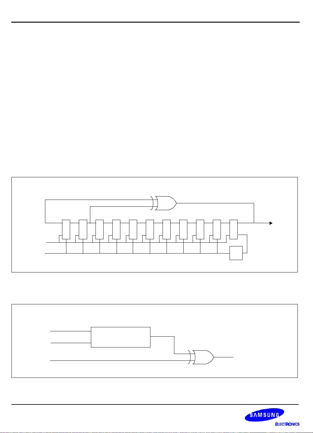
sequence of 2047 bits generated by the recursive linear function X[n] = X[n-11] + X[n-9] (modulo 2). The scrambler
shall generate the specified non-zero key stream whenever the Active Output Interface is required to transmit a
scrambled data stream.
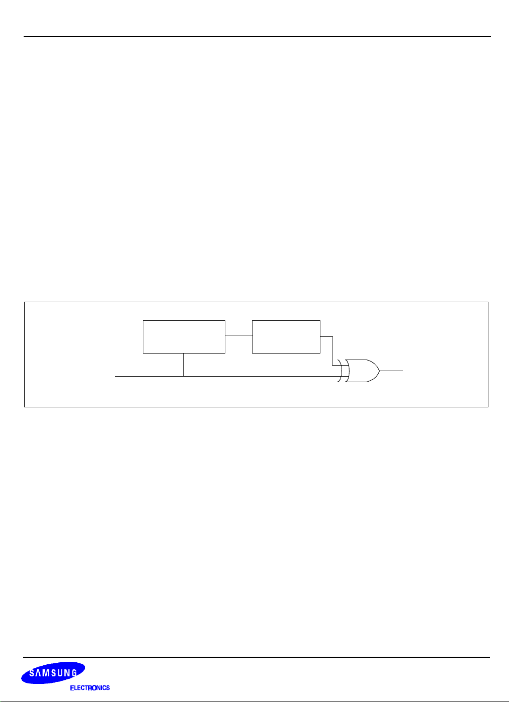
The key steam sequence can be generated by an 11-bit Linear Feedback Shift Register(LFSR) whose input bit is
the exclusive-OR of its 11th and 9th previous bits, and which contains at least one non-zero bit. The functional
diagram for the LFSR is given Figure4-5 whereas a functional block diagram of the scrambler s in Figure4-6.
Tx_clk
Tx_en
Tx_clk
Tx_en
TX_bit
Rst
Figure 4-5. Linear Feedback Shift Register (LFSR)
LFSR
lfsr_out
cipher-text_out
Figure 4-6. Scrambler Function of KS8910
D0D1D2D3D4D5D6D7D8D9D10
cl/st
Q0Q1Q2Q3Q4Q5Q6Q7Q8Q9Q10Q11
lfsr_out
4-10
Page 38
Preliminary Spec. ver 1.4
KS8910 100/10 Mbps ETHERNET TRANSCEIVER 100BASE-TX DIGITAL BLOCKS
Descrambler
The Descrambler shall decode the NRZ cipher-text bit stream from the MLT-3 decoder. The cipher-text bit stream
shall be decoded by addition (modulo 2) of a key stream to produce a plain-text bit stream. The key stream shall be
the periodic sequence of 2047 bits generated by the recursive linear function X[n] = X[n-11] + X[n-9] (modulo 2).
The descrambler shall generate the specified key stream while it is synchronized.
The descrambler is defined to be synchronized while the descrambler key stream added to a sequence of ciphertext bits is identical to the upstream scrambler key stream added to those bits. While the descrambler is
synchronized, error free bits in the cipher-text stream decode as error free bits in the plain-text stream, and errored
bits in the cipher-text stream decode as errored bits in the plain-text stream.
The descrambler shall acquire synchronization on receipt of 60 consecutive error-free cipher-text bits of the Idle
Line State (ILS) pattern while SIGNAL_DETECT is asserted and the output of the MLT-3 decoder is valid:
In the KS8910, the hybrid mode is supported, the descrambler will, therefore, acquire synchronization on receipt of
30 consecutive error-free cipher-text bits of the JK symbol sequence while SIGNAL_DETECT is asserted and the
output of the MLT-3 decoder is valid.
A functional block diagram of the Descrambler is given in Figure4-7.
cipher-text
Lock
Acquisition
LFSR
lfsr_out
Figure 4-7. Descramble Function of KS8910
plain-text_out
4-11
Page 39
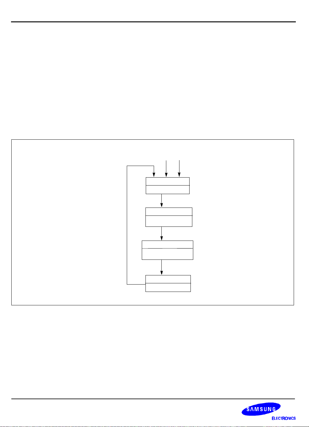
Preliminary Spec. ver 1.4
100BASE-TX DIGITAL BLOCKS KS8910 100/10 Mbps ETHERNET TRANSCEIVER
LINK MONITOR
The Link Monitor process is responsible for determining whether the underlying receive channel is providing
reliable data. Failure of the underlying channel typically causes the PMA’s client to suspend normal actions. The
Link Monitor process takes advantage of the PMD sublayer’s continuously-signaled transmission scheme, which
provides the PMA with a continuous indication of signal detection on the channel through SIGNAL_STATUS as
communicated by the PMD_SIGNAL.indicated primitive. It responds to control by Auto-negotiation.
The Link Monitor process monitors SIGNAL_STATUS and sets link_status to FAIL whenever SIGNAL_STATUS is
OFF or when Auto-negotiation sets link_control to DISABLE. The link is deemed to be reliably operating when
SIGNAL_STATUS has been continuously ON for a certain period of time. If so qualified, Link Monitor sets
link_status to READY in order to synchronize with Auto-negotiation. Auto-negotiation permits full operation by
setting link_control to ENABLE. Figure4-8 shows the state diagram for the Link Monitor
BEGIN(pwon_reset)
(SIGNAL_STATUS = OFF) +
(link_control = DISABLE) +
(faulting = TRUE)
LINK DOWN
link_status=FAIL
link_control = SCAN_FOR_CARRIER
Figure 4-8. Link Monitor State Diagram of KS8910
SIGNAL_STATUS = ON
HYSTERESIS
Start stabilize_timer
stabilize_timer_done
LINK READY
link_status=READY
link_control = ENABLE
LINKUP
link_status=OK
4-12
Page 40
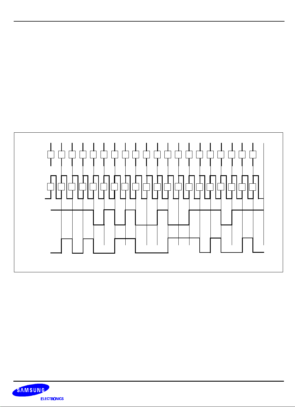
Preliminary Spec. ver 1.4
KS8910 100/10 Mbps ETHERNET TRANSCEIVER 100BASE-TX DIGITAL BLOCKS
NRZ TO NRZI AND NRZI TO NRZ CONVERSION
An NRZ to NRZI and NRZI to NRZ conversion module is designed into the KS8910 chip.This conversion can be
bypassed, and is controllable through a register bit.
The NRZ to NRZI module converts the signal from NRZ to NRZI as follows: The converter module samples the
input at the center of each bit period. If it sees a ONE, the output will shift at the beginning of the next bit period.
This transition can be high to low or low to high. If the converter module sees a ZERO, the output will remain
unchanged for another bit period.
The NRZI to NRZ module converts the signal from NRZI to NRZ as follows: If the input remains unchanged from 1bit period, then the converter module will output a ZERO. If there is a change, then a ONE will be output.
Data Bit
Bit Clock
NRZ Data
NRZI Data
1 1 1 1 0 1 0 1 0 0 1 0 0 1 1 1 0 1 1 1
1 2 3 4 5 6 7 8
9
10 111312 14 15 16
001111 0 00 0 1111111 0 1
17
18 19 20
Figure 4-9. NRZ to NRZI Conversion of KS8910
4-13
Page 41

Preliminary Spec. ver 1.4
100BASE-TX DIGITAL BLOCKS KS8910 100/10 Mbps ETHERNET TRANSCEIVER
PHYSICAL MEDIUM DEPENDENT SUBLAYER
The majority of the PMD is either analog or mixed-signal and is, therefore, not described in this charter, though a
resume is given just below. A detailed description of this part of the circuitry can be found in chapter 6 of this
document.
In the transmit direction the serial data stream is converted from NRZI to MLT-3.
In the inbound direction the DC level of the signal is first restored, then it runs through an equalizer and finally it
gets converted from MLT-3 to NRZI format. Then the clock as well as data are recovered and forwarded to the
PMA.
4-14
Page 42

Preliminary Spec. ver 1.4
KS8910 100/10 Mbps ETHERNET TRANSCEIVER 10BASE-T DIGITAL BLOCKS
5 10 BASE-T DIGITAL BLOCKS
OVERVIEW
The 10BASE-T Ethernet Interface Transceiver subsystem performs the physical layer signaling (PSL) and Media
Attachment Unit (MAU) functions as defined by the IEEE 802.3 specification. It functions as a PLS-only device as
an Integrated PLS/MAU (for use with 10BASE-T twisted-pair networks).
The 10BASE-T Ethernet interfaces a back-end controller to a twisted-pair (TP) cable. The controller interface
includes transmit and receive clock and NRZ data channels, as well as mode control logic and signaling. The
twisted-pair interface comprises two circuits: Twisted-Pair Input (TPI) and Twisted-Pair Output (TPO). In addition to
the three basic interfaces, the 10BASE-T Transceiver has synthesized clocks derived from a 25 MHz crystal oscillator and five LED drivers for visual status reporting.
Functions are defined from the back end controller side of the interface. The 10BASE-T Transceiver function refers
to data transmitted to the twisted-pair network (Integrated PLS/MAU mode). The10BASE-T Ethernet Interface
Receive function refers to data received by the back end from the twisted-pair network (Integrated PLS/MAU
mode). In the integrated PLS/MAU mode, the 10BASE-T Ethernet Interface performs all required MAU functions
defined by the IEEE 802.3 10BASE-T specification such as collision detection, link integrity testing, signal quality
error messaging, jabber control and loopback.
TRANSMIT FUNCTION
The 10BASE-T transceiver receives NRZ data from the controller at the TXD input (see 10/100-Mbit/s transceiver
block diagram of KS8920 ), and passes it through a Manchester encoder. The encoded data is transferred to the
twisted-pair network . The advanced integrated pulse shaping and filtering network produces the output signal on
TPON and TPOP, shown in the Chapter 9,” Timming” section. The TPO output is pre-distorted and prefiltered to
meet the 10BASE-T jitter template. No external filters are required. During idle periods, the 10BASE-T transceiver
transmits link integrity test pulses on the TPO circuit integrated PLS/MAU mode is selected.
JABBER CONTROL FUNCTION
Figure 5-1 is a state diagram of the 10BASE-T Transceiver Jabber control function. The 10BASE-T Transceiver onchip watchdog timer prevents the DTE from locking into a continuous transmit mode. When a transmission exceeds
the time limit, the watchdog timer disables the transmit and loopback functions, and activates the JAB pin. Once the
10BASE-T is in the jabber state, the TXD circuit must remain idle for a period of 0.25 to 0.75 seconds before it will
exit the jabber state.
5-1
Page 43
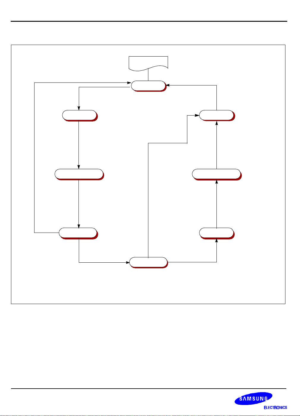
Preliminary Spec. ver 1.4
10BASE-T DIGITAL BLOCKS KS8910 100/10 Mbps ETHERNET TRANSCEIVER
Reset
(1)Unjab
TimerEq0=‘1’
JC_UNJAB
jc_set_UnJabTimer=’0’
DO_active
JC_IDLE
jc_set_TxMaxTimer=’1’
jc_en_TxMaxTimer=’1’
JC_IDLE_1w
jc_dis_XMIT=’0’
jc_ci_sqe=’0’
jc_set_TxMaxTimer=’0’
jc_clr_TxMaxTimer=’0’
jc_en_TxMaxTimer=’0’
jc_set_sr_JabberStatus=’0’
jc_set_UnJabberStatus=’0’
jc_set_UnjabberStatus=’0’
jc_set_UnJabberTimer=’0’
jc_en_unJabberTimer=’0’
(1) DO_active
JC_NONJAB_1w
jc_set_TxMaxTimer=’0’
JC_NONJAB
jc_set_sr_jabberStatus=’1’
(2) DO_active &&
TxMaxTimerEq &&
cr_Jaben=’1’
Figure 5-1. State Diagram of Jabber Control Function
(2)DO_active=’1’
JC_JAB_1w
jc_dis_XMIT=’1’
jc_dis_LPBK=’1’
jc_ci_sqe=’1’
jc_set-sr_JabberStatus=’0’
JC_UNJAB_1w
jc_dis_XMIT=’1’
jc_dis_LPBK=’1’
jc_ci_sqe=’1’
jc_set-UnjabTimer=’1’
jc_en_UnjabTimer=’1’
JC_JAB
DO_active=’0’
5-2
Page 44
Preliminary Spec. ver 1.4
KS8910 100/10 Mbps ETHERNET TRANSCEIVER 10BASE-T DIGITAL BLOCKS
SQE FUNCTION
The 10BASE-T transceiver supports the signal quality error (SQE) function as shown in Figure 5-3. If SQE register
is enabled after every successful transmission on the 10BASE-T network, the 10BASE-T transceiver transmits the
SQE signal to the DTE for ten 5 bit times over the internal CI Circuit.
If SQE is disabled, the 10Base-T transceiver does not transmit SQE signal.The default value of SQE register is disable.
DO_active
XMIT_EN
CLK(20MHz)
wait 1us after
transmit finished
signal 1us
Generation sqet
Figure 5-2. SQE Function
sqet_ci_sqe
RECEIVE FUNCTION
The 10BASE-T transceiver receive function acquires timing and data from the twisted-pair network (the TPI circuit)). Valid received signals are passed through the on-chip filters and Manchester decoder and output as decoded
NRZ data and receive timing on the RXD and RCLK pins, respectively. No external filters are required. An internal
intelligent squelch function discriminates noise from link test pulses and valid data streams. The receive function is
activated only by valid data streams above the squelch level and with proper timing. If the differential signal at the
TPI circuit inputs falls below 75% of the threshold level (unsquelched) for eight bit times (typical), the 10BASE-T
transceiver receive function enters the idle state. If the polarity of the TPI circuit is reversed, the 10BASE-T transceiver detects the polarity reversal and reports it via the PLR output. The 10BASE-T transceiver automatically corrects reversed polarity.
POLARITY REVERSE FUNCTION
The 10BASE-T transceiver polarity reverse function uses both link pulses and end-of-frame data to determine the
polarity of the received signal. A reversed polarity condition is detected when eight opposite receive link pulses are
detected without receipt of a link pulse of the expected polarity. Reversed polarity is also detected if four frames are
received with a reversed start-of-idle. Whenever polarity is reversed, these two counters are reset to zero. If the
10BASE-T transceiver enters the link fail state and no valid data or link pulses are received within 96 to 128 ms the
polarity is reset to the default non-flipped condition. If Link Integrity Testing is disabled, polarity detection is based
only on received data. The polarity reverse function can be controlled by B10CR register.
5-3
Page 45
Preliminary Spec. ver 1.4
10BASE-T DIGITAL BLOCKS KS8910 100/10 Mbps ETHERNET TRANSCEIVER
COLLISION DETECTION FUNCTION
The collision detection function operates on the twisted-pair side of the interface. A collision is defined as the simultaneous presence of valid signals on both the TPI circuit and the TPO circuit. The 10BASE-T transceiver reports
collisions to the back-end via the COL pin. If the TPI circuit becomes active while there is activity on the TPO circuit,
the TPI data is passed to the back-end over the RXD circuit, disabling normal loopback. Figure 5-3 is a state diagram of the 10BASE-T transceiver collision detection function.
CI
(collision Input)
CID_IDLE
CI=’1’
CID_S1_1w
CI=’1’
CID_S1
CI=’0’
CID_S1O_1w
CID_S1O
CI=’0’
Collision State
Machine
Reset or
default
CID_IDLE_w
CI=’1’
cid_Col=’0’
cid_Col=’0’
CI=’0’
CI=’1’
CI=’1’
cid_COL
(collision detected)
CID_SO1O
CID_SO1O_1w
CI=’0’
CID_S1O1
5-4
cid_Col=’0’
’(collision detec)
CID_S1O1_1w
Figure 5-3. State Diagram of Collision Detection Function
Page 46
Preliminary Spec. ver 1.4
KS8910 100/10 Mbps ETHERNET TRANSCEIVER 10BASE-T DIGITAL BLOCKS
LOOP-BACK FUNCTION
The 10BASE-T Transceiver provides the normal loopback function specified by the 10BASE-T standard for the
twisted-pair port. The loopback function operates in conjunction with the transmit function. Data transmitted by the
back-end is internally looped back within the 10BASE-T Transceiver from the TXD pin through the Manchester
encoder/decoder to the RXD pin and returned to the back-end. The normal loopback function is disabled when a
data collision occurs, clearing the RXD circuit for the TPI data. Normal loopback is also disabled during link fail and
jabber states.
The 10BASE-T Transceiver also provides three additional loopback functions. An external loopback mode, useful
for system-level testing, is controlled by LEDC. When LEDC is tied low, the 10BASE-T Transceiver disables the
collision detection and internal loopback circuits, to allow external loopback or full duplex operation. The 10BASE-T
Transceiver provides additional forced loopback functions controlled by LBK BMCR Register Bit. When the TP port
is selected and LBK=1, TP loopback is forced, overriding collisions on the TP circuit. When LBK=0, normal loopback is in effect.
LINK INTEGRITY TEST
Figure 5-4 is a state diagram of the 10BASE-T Transceiver Link Integrity test function. The link integrity test is used
to determine the status of the receive side twisted-pair cable. Link integrity testing is enabled when the LI pin is tied
high. When enabled, the receiver recognizes link integrity pulses which are transmitted in the absence of receive
traffic. If no serial data stream or link integrity pulses are detected within 50-150 ms, the chip enters a link fail state
and disables the transmit and normal loopback functions. The 10BASE-T Transceiver ignores any link integrity
pulse with an interval less than 2~7 ms. The 10BASE-T Transceiver will remain in the link fail state until it detects
either a serial data packet or two or more link integrity pulses.
lipd_link_test_rcv
DO_active
RD_active
link test min timer
link test max timer
10Base-T
Link Status
Monitoring &
Control
link loss timer
Figure 5-4. State Diagram of Link Integrity Test Function
lnk_st_B10[1:0]
lit_dis-XMIT,
lit_dis_RCV,
lit_dis_LPBK
5-5
Page 47

Preliminary Spec. ver 1.4
10BASE-T DIGITAL BLOCKS KS8910 100/10 Mbps ETHERNET TRANSCEIVER
MEMO
5-6
Page 48
Preliminary Spec. ver 1.4
KS8910 100/10 Mbps ETHERNET TRANSCEIVER 100BASE-TX ANALOG BLOCKS
6 ANALOG BLOCKS
OVERVIEW
The 100Base-TX Analog block interfaces the digital logic to the transmit and receive twisted-pair interfaces. A block
diagram of the 100Mbit/s data path is shown in Figure6-1. The 100Mbit/s digital components are described in
Chapter 4. The analog components are shaded and are described in this chapter.see figure 6-2 for the analog
block of the KS8910.
The main transmit analog blocks are the frequency synthesizer and the transmitter. The receive blocks include a
receive buffer, an adaptive equalizer, a baseline restore circuit, and clock recovery. In addition, the receive circuit
detects the presence of on the receive twisted pair and supplies status signals to the autonegotiation circuit
indicating lock detect and signal detect.
A few board-level passive components are required to support the analog circuits. These components include a 25
MHz crystal, a reference bias resistor, but the chip loop filters for the transmit and receive PLLs is integrated on
chip.
100Mbit/s Digital Blocks
100Mbit/s Analog Blocks
4B5B
MII
5B4B
25Mhz
Scrambler
Descrambler
Figure 6-1. 100Mbit/s Data Path Block Diagram of KS8910
Frequency
Synthesizer
Baseline Restore
Clock
Recovery
Transmitter
Adptive
Equalization
Chip
Cat.5 UTP
Transformer
Cat.5 UTP
Board
6-1
Page 49
Preliminary Spec. ver 1.4
100BASE-TX ANALOG BLOCKS KS8910 100/10 Mbps ETHERNET TRANSCEIVER
The 10Base-T Analog block interfaces the digital logic to the transmit and receive twisted-pair interfaces. A block
diagram of the 10Mbit/s data path is shown in Figure6-2. The 10Mbit/s digital components are described in
Chapter 5. The analog components are shaded and are described in this chapter.
10Mbit/s Analog Block
TXPLL
100M
10M
100M
10M
WAVE SHAPER
RXPLL
DPLL
MLT-3
BW EQ
DRIVER
100M
RX EQ
SD
10M
RX SQ
TPOP
TPON
TPIP
TPIN
Figure 6-2. Analog Blocks of KS8910
The main transmit analog blocks are the clock generator, the wave shaper, and the driver. The receive blocks
include a receive buffer . In addition, the receive circuit detects the presence of on the receive twisted pair and
supplies status signals to the auto-negotiation circuit indicating lock detect and signal detect.
A few external components are required to support the analog circuits. These components include a 25MHz
oscillation circuit and a current reference bias circuit.
100MBIT/S TRANSMIT CIRCUITS
The 100 Mbit/s Transmit analog block generates the clocks required for data transmission and drives the twisted
pair. An on-chip PLL synthesizes a 125 MHz clock from a 25 MHz crystal reference. The 100Base-TX Transmit
Driver provides an output capable of driving a transformer-coupled unshielded twisted pair.
6-2
Page 50
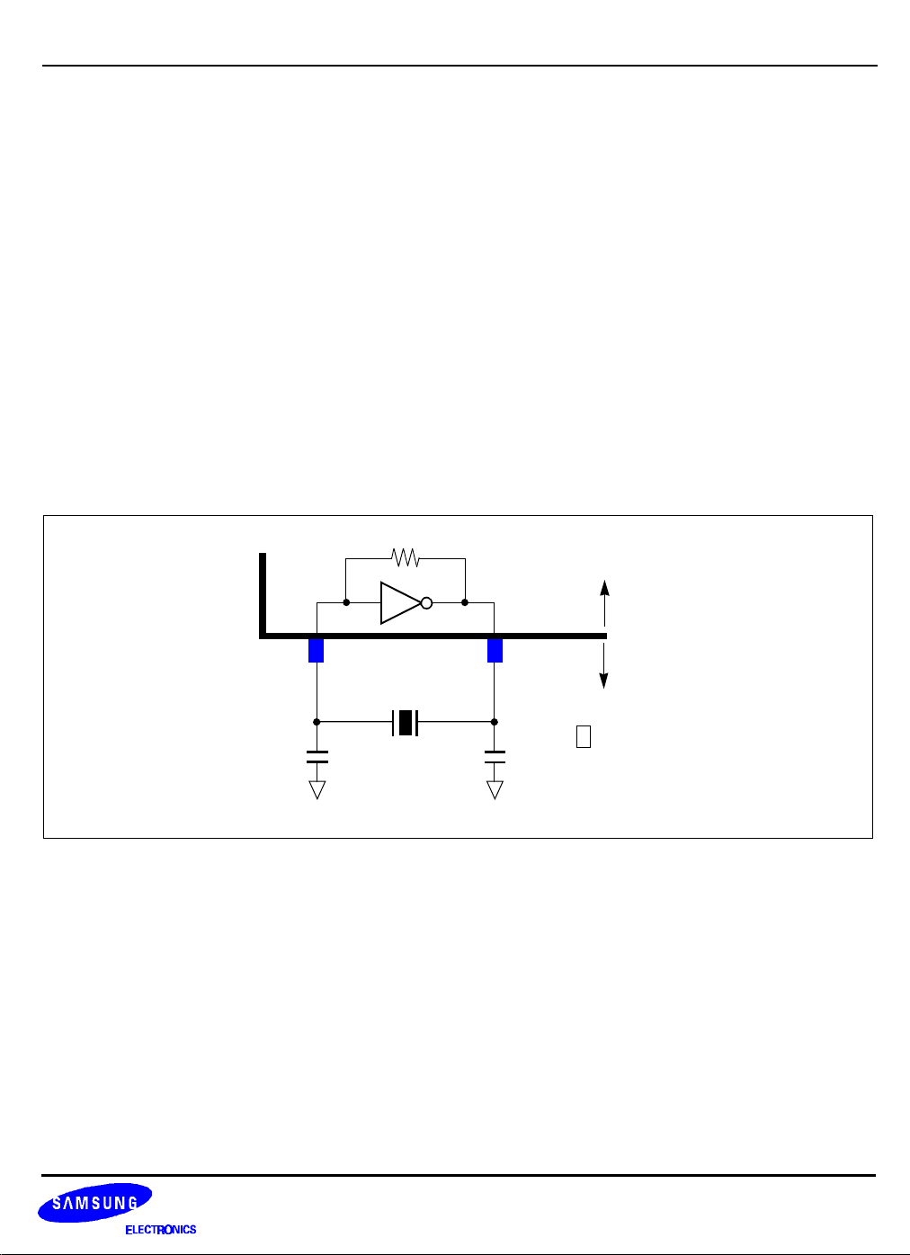
Preliminary Spec. ver 1.4
KS8910 100/10 Mbps ETHERNET TRANSCEIVER 100BASE-TX ANALOG BLOCKS
FREQUENCY SYNTHESIZER
The frequency synthesizer generates all of the clocks required by the chip. A 25MHz parallel resonant crystal is
connected to the on-chip oscillator. This reference frequency drives an on-chip frequency synthesis PLL that
multiplies the 25MHz clock by five to generate a 125MHz clock.
Also this block generates the 2.5MHz, 5.0MHz, and 10MHz clocks for 10Mbit/s.The clock synthesizer generates all
of the clocks required by the netlist. This reference frequency drives an on-chip frequency clock synthesizer that
generates 20MHz clock phases used in the analog and digital sections of the PHY.
CRYSTAL OSCILLATOR
An on-chip Pierce oscillator generates the transmit frequency reference. The recommended connection of the
crystal to the oscillator circuit is shown in Figure6-3. A 25 MHz ±50ppm fundamental mode parallel resonant
crystal should be used. The values of the loading capacitors should be adjusted to match the recommended
loading for the crystal used. The recommended crystal is loaded with 15pF capacitors as shown in Figure6-3.
The external crystal and loading capacitors are connected between the XTAL_IN and XTAL_OUT pins of KS8910 .
KS8910
Chip
XTAL_IN
PIn 15
15pF
XTAL_OUT
Pin14
15pF
GNDGND
Board
Figure 6-3. Crystal Oscillator Connection
Transmit PLL
The frequency synthesis PLL generates a 125 MHz clock from the 25 MHz frequency reference. The PLL uses a
phase-frequency detector, a charge pump, and an voltage controlled oscillator (VCO).
A differential loop filter is integrated on chip. This loop filter forms a second-order loop. Higher order high frequency
filtering is performed on-chip. The VCO gain is 100 MHz/Volt, and the charge pump current is 20 uA. The
recommended components result in a loop bandwidth of 250 KHz and a phase margin of 75 degrees.
6-3
Page 51
Preliminary Spec. ver 1.4
100BASE-TX ANALOG BLOCKS KS8910 100/10 Mbps ETHERNET TRANSCEIVER
Clock Dividers
The frequency synthesizer is completed by a clock divider circuit that generates the remaining clocks required by
the design. The clocks and their uses are summarized in Table 6-1.
Table 6-1. Transmit Clocks Generated by the Frequency Synthesizer
Clock Use
clk125 100 Mbit/s Transmit Logic
clk25 100 Mbit/s MII and Digital
clk10 10 Mbit/s Digital
clk2.5 10 Mbit/s MII
clk20 10 Mbit/s Analog
TRANSMIT TWISTED-PAIR DRIVER
The Transmit Twisted-Pair Driver drives current into the transmit transformer. The combination of the driver and the
transformer must meet the ANSI FDDI TP-PMD template specification. External resistors are used to generate a
reference current and to match the driver to the impedance of the twisted-pair transmission line. These external
resistors must have accuracy of ±1%.
A block diagram showing connection of the driver to the transformer is shown in Figure6-4. The recommended
transformer has a turns ratio of 1(second coil) : (first coil). However, turns ratios lower than 1(second coil) :
(firstcoil)will not enable full 10 Mb/s voltage swing, and higher turns ratios will result in higher power dissipation.
2
2
A Pulse ,Valor, XFMRS’s transformer can meet the application requirements.Please refer to “Application Notes”.
The 100 Mbit/s driver is connected in parallel with the 10 Mbit/s driver to the TPOP and TPON pins. The chip
automatically switches between the two drivers depending on the state of the autonegotiation circuit and the
Control register (Reg 0). Care should be taken on the board layout to minimize parasitic capacitance and
inductance on traces connecting these pins to the transformer.
The recommand transceiver is Halo Co’s “TG110-S131N2”,Pulse Co’s “H001”, “H0010”, “H1033”, “H1035”,
“H1095” and Valor Co’s “ST6122”, “ST6149”.
6-4
Page 52
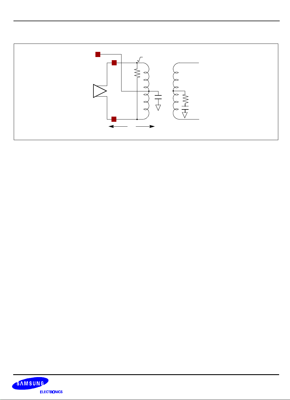
Preliminary Spec. ver 1.4
KS8910 100/10 Mbps ETHERNET TRANSCEIVER 100BASE-TX ANALOG BLOCKS
TPOB
TPOP
200Ω
±1%
CT
2
1 CT
Cable
Chip
0.1uF
TPON
Board
75Ω
±1%
0.1uF
Figure 6-4. Transmit Twister-Pair Driver and Transmit Transformer
Voltage Reference
An on-chip band-gap reference calibrates the output voltage swing. This reference generates an on-chip voltage
voltage reference with an error of ±2.5%. The twisted-pair output voltage swing is proportional to the band-gap
voltage times the impedance matching resistance divided by the current reference resistance. The overall accuracy
of this output swing must be ± 5%.
Current Reference
An on-chip current reference circuit generates the transmit current from the band-gap reference and the external
current reference resistor, RRef. This reference resistor should be connected between ground and the RB pin. The
transmit output current is given by 25Kohm.
100MBIT/S RECEIVE CIRCUITS
The receive circuits include a receive buffer, an adaptive equalizer, a baseline restore circuit, and clock recovery.
The outputs of the analog receive block are data on 100RXD and a recovered clock on 100RXClk. The presence of
a receive signal is signaled as RX Signal Detect. The clock recovery lock detect is signaled on RXClk Lock.
RECEIVER BUFFER
A receive buffer is used to isolate the internal circuits from common mode noise that remains at the transformer
output. The common mode rejection ratio of the receive buffer is at least 40 dB at DC and 20dB at 100 MHz.
The input voltage at the input should be ±400mV differential. The receive buffer automatically generates its
common mode input reference. This allows operation with AC coupled signals. A voltage division and transmission
line termination is performed by the circuit shown in Figure6-5.
6-5
Page 53
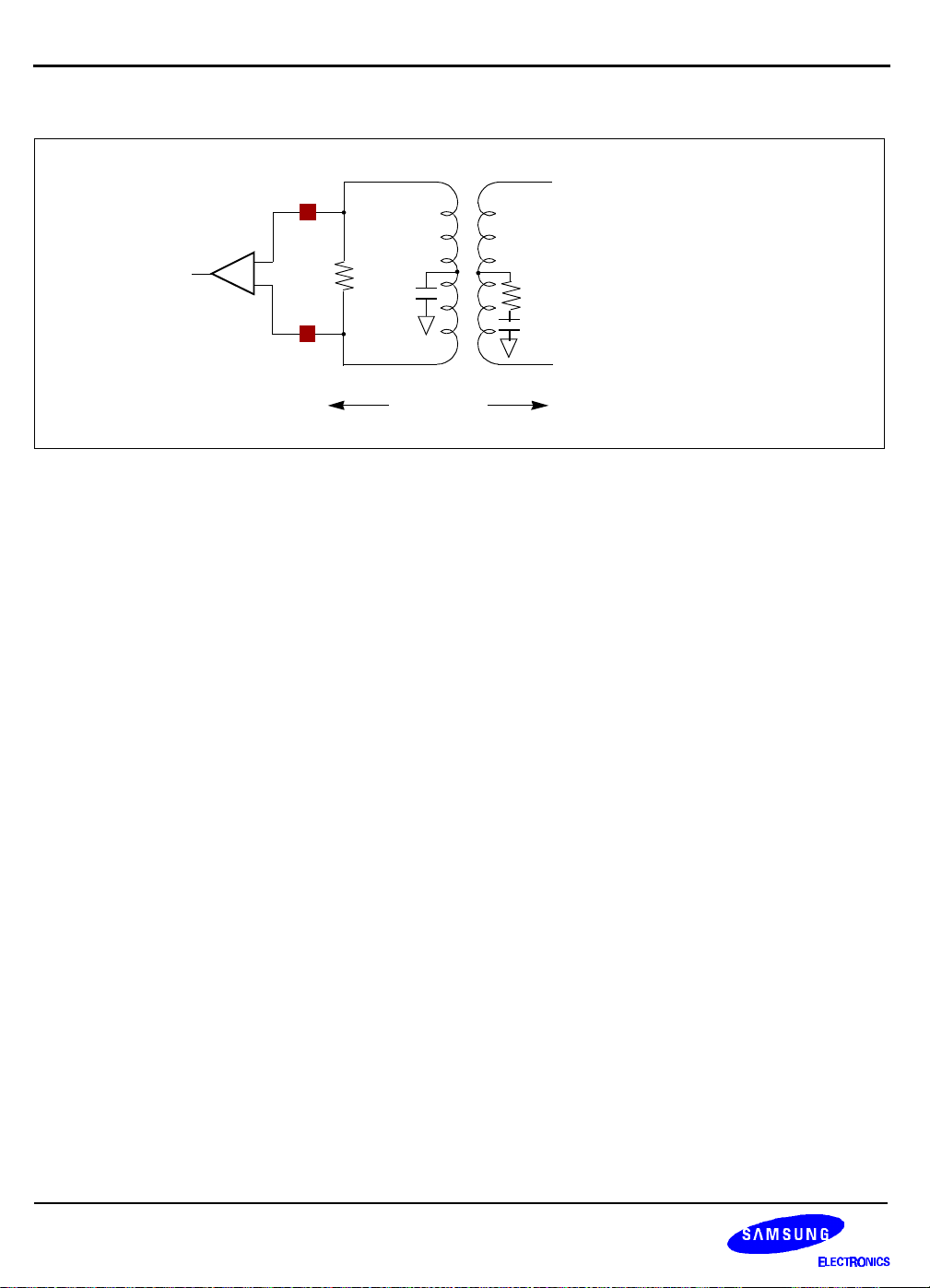
Preliminary Spec. ver 1.4
100BASE-TX ANALOG BLOCKS KS8910 100/10 Mbps ETHERNET TRANSCEIVER
1 CT
TPIP
100Ω
0.1uF
TPIN
Chip
1 CT
all resistors are 1%
75Ω
0.1uF
Board
Figure 6-5. Receive Buffer Circuit Configuration
ADAPTIVE EQUALIZER
High frequency attenuation and group delay variation introduced by the twisted pair degrades the data signal. The
adaptive equalizer restores these high frequency components and restores the data to a condition suitable for clock
recovery and data slicing.
The signal arriving at the receiver after propagation through a 100 meter unshielded twisted pair exhibits a
completely closed eye diagram. The adaptive equalizer restores this eye to a >90% open state. The equalizer is
capable of restoring data transmitted over cables from 0 meters in length to 125 meters in length.
The adaptive equalizer requires no external filter components and no external user interaction. It is capable of
equalizing NRZ or MTL-3 data.
BASE LINE RESTORE
Baseline wander caused by long run lengths in data is compensated by the baseline restore circuit. Run lengths as
long as 57 bits are possible on 100Base-TX. It is impractical to build transformers that display droop times long
enough to recover data of this run length.
The baseline restore circuit uses a nonlinear signal processing technique to restore data signals that have drooped
due to excessive run lengths.
The circuit also further opens the eye. Residual jitter after equalization and baseline restoration is less than 300 ps.
This decreases the jitter tolerance of the clock recovery circuit.
CLOCK RECOVERY
An on-chip frequency synthesis PLL generates a 125MHz clock from the 25 MHz frequency reference. The Clock
Recovery circuit generates a 125Mhz clock and re-timed data from the equalized signal and The PLL uses a
phase-frequency detector, a charge pump, and integrated voltage controlled oscillator (VCO).
6-6
Page 54

Preliminary Spec. ver 1.4
KS8910 100/10 Mbps ETHERNET TRANSCEIVER 100BASE-TX ANALOG BLOCKS
A differential loop filter is integrated on chip. This loop filter forms a second-order loop. Higher order high frequency
poles are added by on-chip filters. The VCO gain is 140MHz/Volt, and the charge pump current is 20uA. The
recommended components result in a loop bandwidth of 250KHz and a phase margin of 75 degrees.
SIGNAL DECTECTOR
The Signal Detector monitors signal amplitude on cable and inform Digital Block about existence of 100
Rx_code_bit by checking link_status. Threshold of Detect Assertion is 400mVp-p and Detect Deassertion is
300mVp-p.
10MBIT/S TRANSMIT CIRCUITS
The 10Mbit/s Transmit analog block generates the clocks required for data transmission and drives the twisted pair.
An oscillation circuit synthesizes clocks from a 25MHz crystal reference. The 10Base-T Transmit Driver provides
an output capable of driving a transformer-coupled unshielded twisted pair. The Clock generator block, Wave
shaper block and Driver block is combined use with 100Mbit/s Analog Block.
TRANSMIT WAVE SHAPER
The Transmit Wave Shaper takes a manchester encoded bit-stream and converts it into a waveshape that fits the
IEEE 802.3 template. refer to IEEE802.3u
10MBIT/S RECEIVE CIRCUITS
The receive circuits include a receive buffer, an adaptive equalizer, a baseline restore circuit, and receive clock
recovery. The outputs of the analog receive block are data on 10RXD and a recovered clock on 20RXClk. The
presence of a receive signal is signaled as RXSignal Detect. The clock recovery lock detect is signaled on
RXClkLock.
RECEIVER
The 10Base receiver has three function blocks : attenuator, receiver, and squelch generator. The attenuator
receives signal range which is specified in the IEEE802.3 and has DC biased at 1.8V. The attenuator is to ensure
the largest input signal amplitude fill below the 3V power supply before feeding the signal to the receiver.
The receiver detects signals with specification listed in IEEE802.3, and generates output signal for the squelch
generator. The squelch generator output a self-time pulse(typical 300ns or 3bit width) triggered by the rising edge
of the sugnal from the receiver. This pulse signals the valid input data is receiving.
The input voltage at the input should be ±585mV differential. The receive buffer automatically generates its
common mode input reference. This allows operation with AC coupled signals. A voltage division and transmission
6-7
Page 55

Preliminary Spec. ver 1.4
100BASE-TX ANALOG BLOCKS KS8910 100/10 Mbps ETHERNET TRANSCEIVER
line termination is performed by the circuit shown in Figure6-5.
RECEIVE CLOCK RECOVERY(20MHZ,DPLL)
An on-chip frequency synthesis PLL recovers a 20MHz clock using the frequency reference from receiving data.
The PLL uses digital techniques to create the optimum clock for re-timinig the received data.
6-8
Page 56

Preliminary Spec. ver 1.4
KS8910 100/10 Mbps ETHERNET TRANSCEIVER REGISTERS
7 REGISTERS
OVERVIEW
The register set is used to control and monitor the 10Base-T/100Base-TX Transceiver chip and can be accessed
through the MII management interface.
All changed bits will become active immediately. That includes the ‘Reset’ and ‘Restart Auto-Negotiation’ bits in the
Base Mode Control Register, BMCR. The software reset, the ‘Reset’ bit in BMCR, will reset the status registers and
all the state machines of the 10Base-T/100Base-TX Transceiver to their default values. All other registers will
maintain their pre-reset values. All required changes of the control registers necessary to obtain a wanted mode of
operation should be carried out before the ‘Reset’ bit is activated. In order to reset all the registers (including the
control registers) and all the state machines of the 10Base-T/100Base-TX transceiver chip to their default value, a
hardware or power-on reset has to take place.
7-1
Page 57

Preliminary Spec. ver 1.4
REGISTERS KS8910 100/10 Mbps ETHERNET TRANSCEIVER
REGISTER DEFINITIONS
Table 8-1. Address Mapping
Register Name Address(Hex) Initial Value B/E
BMCR Base Mode Control Register 0(00h) 0011_0100_0000_0000 B
BMSR Base Mode Status Register 1(01h) 0111_1000_0000_1001 B
PHYIDR1 PHY Identification Register #1 2(02h) 0000_0000_1111_0000 E
PHYIDR2 PHY Identification Register #2 3(03h) 0000_0000_1111_0000 E
ANAR
ANLPAR(BASE PAGE)
ANLPAR(NEXT PAGE) 0000_0000_0000_0000 E
ANER Auto-Negotiation Expansion
ANNPTXR Auto-Negotiation Next Page
Reserved - (08h ~ 0fh) - E
B10CR 10Base-T Control Register 16(10h) 1110_0000_0010_0000 E
TXCR 100Base_TX Control Register 17(11h) 0000_0000_0000_0000 E
PAR PHY Address Register 18(12h) 0000_0000_0000_0000 E
MPTBLE0 MAP Table Register #0 19(13h) 0000_0000_0000_0000 E
MPTBLE1 MAP Table Register #1 20(14h) 0000_0000_0000_0000 E
anacr0 Analog Control Register #0 21(15h) 0000_0000_0000_0000 E
anacr1 Analog Control Register #1 22(16h) 0000_0000_0000_0000 E
anasr Analog Status Register 23(17h) 0000_0000_0000_0000 E
B10SR 10Base-T Status Register 24(18h) 0000_0000_0000_0000 E
TXSR 100Base-TX Status Register 25(19h) 0000_0000_0000_0000 E
RESERVED - (1a ~ 1fh) - E
Auto-Negotiation Advertisement
Register
Auto-Negotiation Link Partner
Ability Register
Register
Transmit Register
4(04h) 0000_0001_1110_0001 E
0000_0000_0000_0001 E
5(05h)
6(07h) 0000_0000_0000_0100 E
7(07h) 0000_0000_0000_0000 E
7-2
NOTE: * The addresses given in table 8-1 are in decimal(hex) while they are hexadecimal in the following tables.
* B/E : Basic/Extended
Page 58

Preliminary Spec. ver 1.4
KS8910 100/10 Mbps ETHERNET TRANSCEIVER REGISTERS
PHY REGISTERS
BASE MODE CONTROL : REGISTER 0
[BMCR] 00h
00h
15 14 13 12 11 10 9 8 7 6 0
PhyRst PhyLoop Sp_Sel An_En PD Isolate Re_AN Dup_Mode Col_Test Reserved
• Col_Test Collision Test 1 = enable Collision signal test
0 = disable Collision signal test(default)
When set, this bit will cause the COL signal to be asserted in response
to the assertion of TX_EN.
• Dup_Mode Duplex Mode 1 = Full Duplex
• Re-AN Restart Auto-negotiation 1 = Restart Auto-negotiation Process
0 = Half Duplex(default)
Duplex selection is allowed when Auto-negotiation is disabled (bit 12 of
this register is cleared). With Auto-Negotiation enabled, this bit does
not reflects the duplex mode.
0 = Normal operation (default)
Re-initiates the Auto-Negotiation process. If Auto-negotiation is AutoNegotiation disabled (bit 12 of this register cleared), this bit has no
function and should be cleared. This bit is self-clearing and will return a
value of 1 until Auto-Negotiation is initiated by KS8925, whereupon it
will self-clear. Operation of the Auto-Negotiation process is not
affected by the management entity clearing this bit.
• Isolate Isolate 0 = Normal operation (default)
1 = Internal MII Isolate(High Impedence)
When this bit is set, the PHY Layer does not respond to TXD[3::0],
TX_EN, and TX_ER inputs, and it presents a ‘0’ on its TX_CLK,
RX_CLK, RX_DV, RX_ER, RXD[3::0], COL and CRS outputs. The
KS8910 still responds to internal management transactions.
• PD Power Down 1 = Power Down Mode
0 = Normal operation (default)
When this bit is set, PHY blocks goes into power down mode.
• AN_En Auto-negotiation Enable 1 = Enable Auto-negotiation Process (default)
• Sp_Sel Speed Selection
0 = Disable Auto-negotiation Process
Bit 8 and 13 of this register are ignored when this bit is set. Bit 8 and 13
determine the link speed and mode if this bit is cleared.
1 = 100 Mbit/s
0 = 10 Mbit/s(default)
Sp_Sel Link speed is selected by this bit or by Auto-negotiation
if bit 12 of this register is set. (In which case, the value of this bit
is ignored)
7-3
Page 59

Preliminary Spec. ver 1.4
REGISTERS KS8910 100/10 Mbps ETHERNET TRANSCEIVER
• PhyLoop PHY Loopback 1 = Enable loop back mode
0 = Disable loop back mode (default)
The loopback function enables MII transmit data to be routed to the MII
receive data path. This loopback will go through the PMA and the RX
clock will be TX clock.
• PhyRst PHY Reset 1 = KS8910 reset
0 = Normal operation (default)
This bit set the status registers and all of the states of PHY to their
default value. This bit, which is self-clearing, returns a value of zero
until the reset process is complete.
7-4
Page 60

Preliminary Spec. ver 1.4
KS8910 100/10 Mbps ETHERNET TRANSCEIVER REGISTERS
BASE MODE STATUS : REGISTER 1
[BMSR] 01h
01h
15 14 13 12 11 10 7 6 0
-
100FD 100HD 10FD 10HD
Reserved
MF Prm Sup AN_Comp Rmt Fault AN_Abt Link _Stat Jab_Det Ext_Cap
• Ext_Cap Extended Capability
• Jab-Det Jabber Detector 1 = Jabber condition detected
• Link_Stat Link Status 1 = Link is up indicates that the XCVR has determined that a valid link
• AN_Abt Auto-Negotiation Ability
• Rmt_Fault Remote Fault 1 = Remote fault detected
• AN_Comp Auto-Negotiation Complete
• MFPrmSup MF Preamble Suppression
• 10HD 10Base-T Half Duplex 1 = 10Base-T Half Duplex capable (permanently set)
• 10FD 10Base-T Full Duplex 1 = 10Base-T Full Duplex capable (permanently set)
• 100HD 100Base-TX Half Duplex 1 = 100Base-TX Half Duplex capable (permanently set)
• 100FD 100Base-TX Full Duplex 1 = 100Base-TX Full Duplex capable (permanently set)
1 = extended register capabilities (permanently set)
0 = basic register set capabilities only
0 = No jabber condition detected. (default)
This bit has meaning only in 10Mbit/s modes.This bit is implemented
with a latching function so that the occurrence of a jabber condition
causes it to become set until it is cleared by a read to this register by
the management interface.
has been established.
0 = Link is down (default)
The link status bit is implemented with a latching function, so that the
occurrence of a link failure condition causes the Link status bit to
become cleared and remain cleared until it is read via the management
interface. After the read, this bit will latch the XCVR link status at the
end of the read.
1 = Auto-negotiation Available (permanently set)
0 = Auto negotiation not available.
0 = No remote fault detected(default)
This bit is cleared on read. When the RF bit in the received base Link
Code Word is set to logic one, this Remote Fault bit will be set to one.
1 = Auto-negotiation Completed
0 = Auto-negotiation not Completed(default)
1 = Accept management frames with preamble suppressed.
0=Not accept management frames with preamble suppressed.
(permanently set)
0 = Not 10Base-T Half Duplex capable
0 = Not 10Base-T Full Duplex capable
0 = Not 100Base-T Half Duplex capable
0 = Not 100Base-TX Full Duplex capable
7-5
Page 61

Preliminary Spec. ver 1.4
REGISTERS KS8910 100/10 Mbps ETHERNET TRANSCEIVER
PHY IDENTIFIER 1 : REGISTER 2
[PHYIDR1] 02h
02h
15 0
OUI_MSB
• OUI_MSB OUI Most Significant Bits OUI MOST SIGNIFICANT BITS: This register stores bits 3 to 18 of the
OUI (000000h) to bits 15 to 0 of this register respectively. The most
significant two bits of the OUI are ignored. The OUI_MSB should be
programmed by the system manufacturer to reflect the OUI assigned
to their organization.
Initial value:0000 0000 1111 0000
PHY IDENTIFIER 2 : REGISTER 3
[PHYIDR2] 03h
15 10 9 4 3 0
OUI_LSB VNDR_MDL MDI_REV
• MDI_REV Model Revision Number Four bits of vendor model revision number mapped to bit 3 to 0 (most
significant bit to bit 3)
Initial value:0000
• VNDR_MDL Vendor Model Number Six bits of vendor model number mapped to bits 9 to 4 (most significant
bit to 9). The VNDR_MDL and MDI_REV should be programmed by
the system manufacturer to reflect the product model and revision
which uses this KS8910.
03h
Initial Value:00 1111
• OUI_LSB OUI Least Significant Bits Bits 19 to 24 of the OUI (000000h) are mapped to bits 15 to 10 of this
7-6
register respectively. The OUI_LSB should be programmed by the
system manufacturer to reflect the OUI assigned to their organization.
Initial Value:0000 00
Page 62

Preliminary Spec. ver 1.4
KS8910 100/10 Mbps ETHERNET TRANSCEIVER REGISTERS
AUTO-NEGOTIATION ADVERTISEMENT : REGISTER 4
[ANAR] 04h
04h
15 14 13 12 11 10 9 8 7 6 5 4 0
NextPg ACK Rmt_Fault 0 0 0 100FullDup 100HalfDup 10FullDup 10HalfDup Selector
• Selector Protocol Selector These bits contain the binary encoded protocol selector supported by
this node. (00001) indicates that this device supports IEEE 802.3
CSMA/CD.
• 10HalfDup 10Base-T Half Duplex 1 = 10Base-T HALF DUPLEX is supported by the KS8910.
0 = 10Base-T HALF DUPLEX is not supported by the KS8910.
• 10FullDup 10Base-T Half Duplex 1 = 10Base-T FULL DUPLEX is supported by the KS8910.
0 = 10Base-T FULL DUPLEX is not supported by the KS8910.
• 100HalfDup
• 100FullDup 100Base-TX Half Duplex 1 = 100Base-TX FULL DUPLEX is supported by the KS8910.
• Rmt_Fault Remote Fault
• ACK
100Base-TX Half Duplex
Acknowledge 1 = Acknowledge the Reception of Link Partner ability.
1 = 100Base-TX HALF DUPLEX is supported by the KS8910.
0 = 100Base-TX HALF DUPLEX is not supported by the KS8910.
0 = 100Base-TX FULL DUPLEX is not supported by the KS8910.
1 = Advertised that this device has detected a Remote Fault.
0 = Not Remote Fault detected.
0 = Not Acknowledge the Reception of Link Partner ability.
.
• NextPg
This field only used in the transmitting/receiving of the link code word.
The XCVR Auto-Negotiation state machine will automatically control
this bit in the outgoing FLP bursts, setting it at the proper time during
the Auto-Negotiation process. Write as zero, ignore on read.
Next Page Indication 1 = Next Page able
0 = Not Next Page able
This KS8910 supports the next page capability.
7-7
Page 63

Preliminary Spec. ver 1.4
REGISTERS KS8910 100/10 Mbps ETHERNET TRANSCEIVER
AUTO-NEGOTIATION LINK PARTNER ABILITY : REGISTER 5
[ANLPAR] 05h : Base Page
05h
15 14 13 12 11 10 9 8 7 6 5 4 0
NP ACK RF Reserved T4 100_FD 100_HD 10_FD 10_HD Selector
• Selector Protocol Selector =00001: These bits contain the binary encoded protocol selector
• 10_HD 10Base-T Half Duplex If set(=1), Linlk Parter supports 10Base-T Half Duplex mode.
• 10_FD 10Base-T Half Duplex If set(=1), Link Parter supports 10Base-T Full Duplex mode.
• 100_HD
• 100_FD 100Base-TX Half Duplex If set(=1), Link Parter supports 100Base-TX Full Duplex mode.
• T4 T4 Support 1= 100Base-T4 is supported by the Link Parter
• RF Remote Fault If set(=1), a Remote Fault is detected by Link Partner.
• ACK
• NP
100Base-TX Half Duplex If set(=1), Link Parter supports 100Base-TX Half Duplex mode.
Acknowledge If set(=1), Link Partner acknowledge the Reception of ability data word.
Next Page Indication. If set(=1), Link Parter supports Next page function.
supported by the Link Partner.
0= 100Base-T4 is not supported by the Link Parter.
[ANLPAR] 05h : Next Page
15 14 13 12 11 10 0
NextPg ACK MsgPg ACK2 Tog Pg_Code
05h
• Pg_Code Page Code If the MsgPg=1, this field will be interpreted as the Message Page.
If the MsgPg=0, this field will be interpreted as the Unformated Page.
• Tog Toggle 1 = Previous value of the toggle bit in the Link Code Word sent by the Link
Partner is ‘0’.
0 = Previous value of the toggle bit in the Link Code Word sent by the Link
Partner is ‘1’.
• ACK2 Acknowledge 2 1 = This has ability to comply with the message.
0 = This has not ability to comply with the message.
• MsgPg
• ACk Message Page If set(=1), Link Partner acknowledges the Reception of a Next Page Link
• NextPg Next Page If set(=1), Link Partner Next Page available.
7-8
Message Page 1 = Formatted message page.
0 = Unformatted message page.
Code Word.
Page 64

Preliminary Spec. ver 1.4
KS8910 100/10 Mbps ETHERNET TRANSCEIVER REGISTERS
AUTO-NEGOTIATION EXPANSION : REGISTER 6
[ANER] 06h
06h
15 5 4 3 2 1 0
0 0 0 0 0 0 0 0 0 0 0 PDF LP_NP_Able NP_Able Page_RX LP_AN_Able
• LP_AN_Able Link Partner AN Able 1 = The Link Partner supports the Auto-Negotiation.
0 = The Link Partner does not support the Auto-Negotiation.
• Page_RX Link Code word Page
Received
• NP_Able Next Page Able This status bit indicates if this XCVR supports Next Page negotiation.
• LP_NP_Able Link Partner Next Page
Able
• PDF Parallel Detection Fault 1 = Parallel Detection Fault. During the Parallel detection, Zero or More
1 = A new Link Code Word has been received. This bit is cleared
automatically when Auto-Negotiation Expansion is read or when a next
page is written to Auto-Negotiation Next Page Transmit register.
0 = New Link Code Word has not been received.
This XCVR is capable of supporting the Next Page negotiation.
1 = This XCVR is Next Page Able. (Permanently Set)
0 = This XCVR is not Next Page Able.
This status bit indicates if the Link Partner supports Next Page
negotiation.
1 = Link Partner is Next Page Able.
0 = Link Partner is not Next Page Able.
than One PMAs indicate that their links are READY.
0 = No Parallel Detection Fault. This PDF bit will be reset to 0 upon a
read of the ANER register.
7-9
Page 65

Preliminary Spec. ver 1.4
REGISTERS KS8910 100/10 Mbps ETHERNET TRANSCEIVER
AUTO-NEGOTIATION NEXT PAGE TRANSMIT REGISTER : REGISTER 7
[ANNPTXR] 07h
07h
15 14 13 12 11 10 0
NextPg ACK MsgPg ACK2 Tog Pg_Code
• Pg_code Page Code If the MsgPg = 1, this field will be interpreted as the Message Page.
• Tog Toggle 1 = Previous value of the Toggle bit in the Link Code Work sent by this
• ACK2 Acknowledge 2 1 = This has ability to comply with the message.
• MsgPg Message Page 1 = Message Page.
• ACK2 Acknowledge 1 = This KS8910 acknowledges the Reception of a Link Code Word.
• NextPg Next Page Indication 1 = This KS8910 is Next Page able
If the MsgPg = 0, this field will be interpreted as the Unformatted Page.
KS8910 is 0.
0 = Previous value of the Toggle bit in the Link Code Work sent by this
KS8910 is 1.
0 = This has not ability to comply with the message.
0 = Unformatted Page.
0 = This KS8910 does not Acknowledge the Reception of a Link Code
Word. Write as ZERO, read don’t care.
0 = This KS8910 is Not Next Page able
7-10
Page 66

Preliminary Spec. ver 1.4
KS8910 100/10 Mbps ETHERNET TRANSCEIVER REGISTERS
10BASE-T CONTROL REGISTER : REGISTER 16
[B10CR] 10h
10h
15 14 13 12 11 10 9 8 6 5 4 3 2 0
LIT Nor-Thd Jab_En SQE_En Reserved DLPBK 0 0 0 PLR . TstMode TMUXSEL
• TMUXSEL Test MUX Selection Not Use
• TstMode Test Mode Reduce the 1us Tick to 0.1 us tick. Reduce the 1ms tick to 50us Tick.
This will speed up the timer test 20 time. The following timer for AutoNegotiation are set to the test initial values when this bit is set.
• Break Link Timer
TestMode = 0: 1400 ms ticks.
TestMode = 1: 7 ms ticks.
• Auto-negotiation Wait Timer
TestMode = 0: 800 ms ticks.
TestMode = 1: 4 ms ticks.
• Link Fail Inhibit Timer
TestMode = 0: 800 ms ticks.
TestMode = 1: 4 ms ticks.
To get out of the test mode, the programmer has to clear this
TstMode
• PLR Link Polarity Reverse
Enable
• DLPBK Data Loopback If set, start 10Base-T Data Loop-Back.
• SQE_En SQE Test Enable 1 = Enable SQE Test Function.
• Jab_En Jabber Enbale
• Nor_Thd Normal Threshold 1 = normal squelch threshold selected. (default)
• LIT Link Integrity Test 1 = Link Integrity Test Enable.(defalut)
1 = Enable Link Polarity Reverse function.
0 = Disable Link Polarity Reverse function.
0 = Disable SQE Test Function(default).
When this KS8910 is configured for 10Base-T Full Duplex operation,
this bit will be ignored.(The collision/SQE function has no meaning in
Full Duplex mode.)
1 = Enable 10Base-T Jabber function. (default)
0 = Disable 10Base-T Jabber function.
0 = reduced squelch threshold selected.
0 = Link Integrity Test Disable. good link condition forced.
7-11
Page 67

Preliminary Spec. ver 1.4
REGISTERS KS8910 100/10 Mbps ETHERNET TRANSCEIVER
100BASE-TX CONTROL REGISTER : REGISTER 17
[TXCR] 11h
11h
15 14 13 12 11 10 9 8 7 6 5 4 3 2 1 0
0 0 0 0 0 0 LPBK BPNRZI 0 0 BP_4B5B BP_SCR DTMode DHybrid IDLESEL
• IDLESEL Select the number of IDLE
Bits for descrambler synchronization:
• DHybrid Hybride Mode 1 = Use both IDLE and IIIJK to achieve Descrambler synchronization.
• DTMode Descrambler Test Mode 1 = Descrambler Lock timeout value is equal to 260 bits.
• BP_SCR Bypass Scrambler 1 = Scrambler and descrambler functions bypassed.
• BP_4B5B Bypass 4B5B 1 = 4B/5B encoder and 5B/4B decoder functions are bypassed.
• BPNRZI Bypass NRZI
• LPBK Loopback 1 = 100Base-TX Loop Back.
00 = 22 IDLE bits (default)
01 = 32 IDLE bits
10 = 42 IDLE bits
0 = Use only IDLE to achieve Descrambler synchronization.
0 = Descrambler Lock timeout value is equal to 2**17 bits(1.048 ms.)
0 = Normal Scrambler/Descrambler operation.
0 = Normal 4B/5B and 5B/4B operation.
1= NRZI By pass(TX/RX).
0= Normal NRZI Operation(TX/RX).(default)
0 = Normal TX/RX.(default)
PHY ADDRESS REGISTER : REGISTER 18
[PAR] 12h
15 5 4 0
Reserved PHYAddr
• PHYAddr Phy Address The values of the ID[4:0] pins are latched into this register at power-up/
reset.
7-12
12h
Page 68

Preliminary Spec. ver 1.4
KS8910 100/10 Mbps ETHERNET TRANSCEIVER REGISTERS
MAP TABLE REGISTER 0 : REGISTER 19
[MPTBLE0] 13h
13h
15 0
Map_Table
• Map_Table Map Table PRF Mux output value of PH~PA is desided by Map_Table[26:0]value.
The initial value of the Map_Table[15:0] is 0000 0000 0000 0000.
Map_Table[26:0]=MPTBLE0[15:0],MPTBLE1[10:0].
MAP TABLE REGISTER 1 : REGISTER 20
[MPTBLE1] 14h
15 14 13 12 11 10 0
Iadj_UP Iadj_S1 IadjS0 SS_Mux Sel_BG Map_Table
• Iadj_UP
• Iadj_S1,Iadj_S0
• SS_Mux Select SS Mux
• Sel_BG Select BG
• Map_Table Map Table[26:16]
PrefilterCnt Data Input Signal comparing level control(RX path data
jitter control)
The initial value of tIadj_S1[15:13] is 0
100M Path Data Input Signal comparing level control.
The initial value of tIadj_S1, ladj_S0 is 00
Select SS Mux for PRF
Select BG Reference Block status for ANSR(Register 23)
The initial value of the map_table[26:16] is 0 000 0000 0000
14h
7-13
Page 69

Preliminary Spec. ver 1.4
REGISTERS KS8910 100/10 Mbps ETHERNET TRANSCEIVER
ANALOG CONTROL REGISTER 0 : REGISTER 21
[ANARC0] 15h
15h
15 8 7 0
QinH ~ QinA PinH ~ PinA
• QinA Equalizer HPF s/w The fixed output value of prefilter counter when Use_PQ(Reg(16.1)=1
• PinA Equalizer BPF s/w Thefixed output value of prefilter counter.
ANALOG CONTROL REGISTER 1 : REGISTER 22
[ANARC1] 16h
16h
15 14 13 12 11 10 9 8 7 6 5 4 3 2 1 0
UPDNB S1 S0 QFCBP FR PDWS PDSQ PDSG PDR PDPF PRRE PDRP PDTP PDDRV USEPQ Qinl
• Qinl TheMSB value of ‘0’ input of prefilter counter.
• USEPQ use PQ
• PDDRV Power down TXPLL Power Down for DRIVER.
• PDTP Power down TXPLL Power Down for TXPLL.
• PDRP Power down RXPLL Power Down for RXPLL.
• PDRE Power down Reference Power Down for Reference and X-tal.
• PDPF Power down Prefilter Power Down for bias bulk of prefilter.
• PDR Power down Reference Power Down for reference.
• PDSG Power down Signal Dectect Power Down for Signal Detect and prefilter.
• PDSQ Power down Squelch Power Down for Squelch(10RX).
• PDWS Power down Waveshaper Power Down for Waveshaper.
• FR Freeze The operation Halt of prefilter counter MUX.
• QFCBP QFC Bypass RXPLL Input data selection between QFCOUTPUT data and external
• S1 ~ S0 Band Gap Reference Level comparing reference.
• UPDNB Band Gap Reference Level comparing reference.
The Initial selection of the output value of prefilter counter.
1 = PQ value select
0 = Normal operatoin value select
input data. If set(=1), Selected external input.
7-14
Page 70

Preliminary Spec. ver 1.4
KS8910 100/10 Mbps ETHERNET TRANSCEIVER REGISTERS
ANALOG STATUS REGISTER : REGISTER 23
[ASR] 17h
17h
15 14 13 12 11 10 9 0
AnaStat
• AnaStat Analog Status Register
If Sel_BG(MTPBLE0[11] bit value,
1 = Selection of Band gap reference value.
0 = Selection of prefilter counter output value[PG~PA,QI~QA]
10BASE-T STATUS REGISTER : REGISTER 24
[B10SR] 18h
15 14 13 12 11 10 9 8 0
XMT RCV COL PLR JAB LNKST FD Reserved
• FD Full Duplex 1 = Full Duplex
• LNKST Link Status 1 = 10Base-T link is up
• JAB Jabber Detected 1 = jabber condition detected
• PLR Polarity Reverse Detected 1 = Polarity Reverse Detected.
• COL Collision Detected 1 = Collision detected.
• RCV Receive active 1 = Active Receive.
• XMT Transmit active 1 = Active Transmit.
0 = Half Duplex.
0 = 10Base-T link is down.
0 = no jabber condition detected
0 = Polarity Reverse not Detected.
0 = Collision not detected.
0 = Receive IDLE.
0 = Transmit IDLE.
18h
7-15
Page 71

Preliminary Spec. ver 1.4
REGISTERS KS8910 100/10 Mbps ETHERNET TRANSCEIVER
100BASE-T STATUS REGISTER : REGISTER 25
[TXSR] 19h
19h
15 14 13 12 11 10 9 8 0
XMT RCV COL Resreved LNKST FD Reserved
• FD Full Duplex
• LNKST Link status 1 = 100Base-TX link is up.
• COL Colision Detected 1 = Collision detected.
• RCV Receive Active 1 = Active Receive.
• XMT Transmit Active 1 = Active Transmit.
1 = Full Duplex.
0 = Half Duplex.
0 = 100Base-TX link is down.
0 = Collision not detected.
0 = Transmit IDLE.
0 = Transmit IDLE.
7-16
Page 72

Preliminary Spec. ver 1.4
KS8910 100/10 Mbps ETHERNET TRANSCEIVER ELECTRICAL CHARACTERISTICS
8 ELECTRICAL CHARACTERISTICS
This chapter describes the electrical characteristics of KS8910 100/10Mbps Ethernet Transceiver. The information
is presented according to the following table of contents.
• Absolute Maximum Ratings
• Recommaned Operating Ranges
• D.C Electrical Characteristics
• Timming
8-1
Page 73
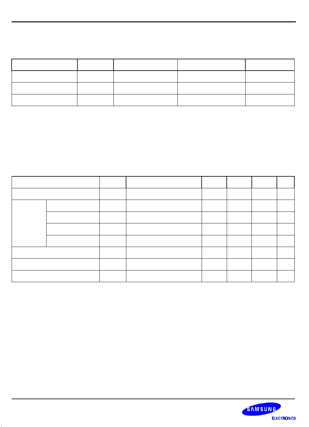
Preliminary Spec. ver 1.4
ELECTRICAL CHARACTERISTICS KS8910 100/10 Mbps ETHERNET TRANSCEIVER
ABSOLUTE MAXIMUM RATINGS
Table 8-1. Absolute Maximum Ratings (T
Parameter Symbol Min Max Unit
Supply Voltage V
Operating Tempatature T
Storage Temperature T
NOTE: Absolute Maximum Ratings may cause critical device failure by above table beyond limits.
DD
OP
STG
RECOMMENDED OPERATING RANGES
Table 8-2. Recommended Operating Conditions
Parameter Symbol Conditions Min Typ Max Unit
Operating Voltage V
Supply
100Base-TX I
Current
10Base-T I
Power-Down Mode I
DD
100TX
10T
PD
= 25 ° C)
A
GND-0.3 3.8 V
0 70 ° C
-65 150 ° C
- 3.1 3.3 3.5 V
- - 180 - mA
- - 200 - mA
- - 300 - uA
Auto-Negotiation I
Ambient Operating Temperature T
X-tal OSC Frequency f
X-tal OSC Frequency Tolerance f
NOTE: The device is guaranteed within above limits.
8-2
AN
OP
OSC
OT
- - 300 - mA
- 0 - 70 ° C
CL = 15pF - 25 - MHz
- -50 - 50 PPM
Page 74

Preliminary Spec. ver 1.4
KS8910 100/10 Mbps ETHERNET TRANSCEIVER ELECTRICAL CHARACTERISTICS
D.C ELECTRICAL CHARACTERISTICS
MII PADS SPECIFICATION
VDD=3.3V¡ 10%, TA=0 to 125° C(5.0V Tolerant I/O)
Table 8-3. MII Pads Specification
Parameter Symbol Conditions Min Typ Max Unit
Input Low Voltage V
Input High Voltage V
Ouput Low Voltage V
Ouput High Voltage V
VDD Supply Current I
PowerDown Current I
Input Low Current I
Input High Current I
NOTES :
1. Only leakage Current
DD
PD
OL
OH
IL
IH
IL
IH
I
OL
I
OH
100BASE-TX TRANSCEIVER SPECIFICATION
VDD=3.3V¡ 10%, TA=0 to 125° C(5.0V Tolerant I/O)
Table 8-4. 100Base-TX Transceiver Specification
Parameter Symbol Conditions Min
- - - 0.8 V
- 2.0 - -
= 6mA - - 0.4
= 6mA 2.4 - -
- - - 100
Note 1 - - -
- -10 - 10
- -10 - 10
1
Typ
Max Unit
V
V
V
uA
uA
uA
uA
Peak Differential Output Voltage V
Over shoot V
Signal Amplitude Symmertry V
Signal Rising/Falling Time TR/T
Signal Rising/Falling Symmertry TSR/T
Jitter V
Duty Cycle Distortion DCD
NOTES :
1. Typical Value are at 25 ° C and are for design aid only;not guaranteed and not suject to prodiction testing.
2. Measured at the line side of the transformer, line replaced by 100ohm(±1%) register.
OUT_100
OV
S
F
SF
JTTR_100
Measured differentially - - 1.4
Offset from 16ns pulse width
Note2 0.95 - 1.05 V
- - - 5
Note2 98 - 102
Note2 3.0 0 5.0
Note2 - - 0.5
at 50% of pulse peak
- - 0.5
%
%
ns
ns
ns
ns
8-3
Page 75
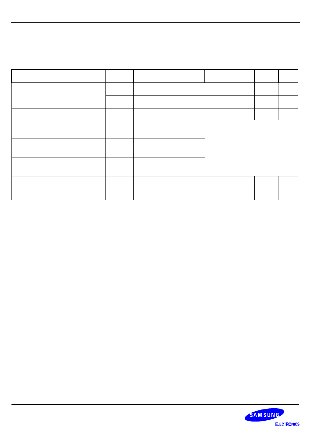
Preliminary Spec. ver 1.4
ELECTRICAL CHARACTERISTICS KS8910 100/10 Mbps ETHERNET TRANSCEIVER
10BASE-T TRANSCEIVER CHARACTERISTICS
VDD=3.3V¡ 10%, TA=0 to 125° C(5.0V Tolerant I/O)
Table 8-5. 10Base-T Transceiver Specification
Parameter Symbol Conditions Min
V
TSQ_I
Normal Threshhold : NTH=1 300 - 585
Typ
1
Differential Squelch Threshold
V
Link Transmit Period T
TPOP/TPON Output Voltage
TSQ_O
Normal Threshhold : NTH=0 180 - 461
LTP
Note2 8 - 24
- Note2
Template
TPOP/TPON Link Pulse Output
Voltage Template
TPOP/TPON TP_IDL Output
- Note2
- Note2
Shown in figure 9-1,9-2,9-3 based
upon IEEE Standard 802.3
Voltage Template
TPOP/TPON Harmonic Distortion THD
Jitter V
NOTES :
1. Typical Value are at 55 ° C and are for design aid only;not guaranteed and not suject to prodiction testing.
2. Measured at the line oppsite side of the transformer.
JTTR_10
Note3
Note4
- - -27
3. Measured at the line side of the transformer.
4. After line model specified by IEEE802.3 for 10Base-T
Max Unit
mV
mV
ms
dB
11
ns
8-4
Page 76
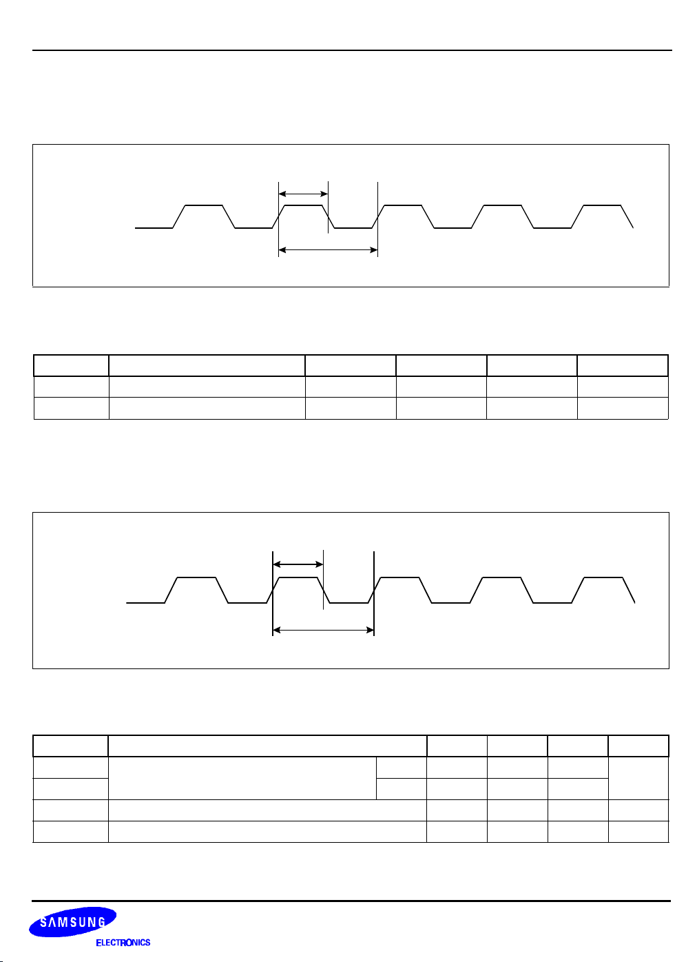
Preliminary Spec. ver 1.4
KS8910 100/10 Mbps ETHERNET TRANSCEIVER ELECTRICAL CHARACTERISTICS
TIMMING
OSC CLOCK FREQUENCY
t
1
Clk_freq
t
2
Figure 8-1. Clock Frequency Timing Diagram
Table 8-6. Clock Frequency
Symbol Conditions Min Typ Max Unit
t1 Clock Freq Dudy Cycle 45 50 55 %
t2 Clock Period - 40 -
ns
NOTES : 1. Clk Freq switching point is 50% if VDD
MII-TRANSMIT CLOCK TOLERANCE
t
1
Tx_clk
t
2
Figure 8-2. MII-Transmit Clock Tolerance Timing Diagram
Table 8-7. MII-Transmit Clock Tolerance
Symbol Conditions Min Typ Max Unit
t1
Tx_clk Duty Cycle
100M 35 60 65
10M 35 50 65
t2a Tx_clk Period (100Base-TX / MII Interface) - 40 -
t2b Tx_clk Period (10Base-T / MII Interface) - 400 -
%
ns
ns
NOTES : 1.TX_clk Duty Cycle switching point is 50% if VDD
8-5
Page 77
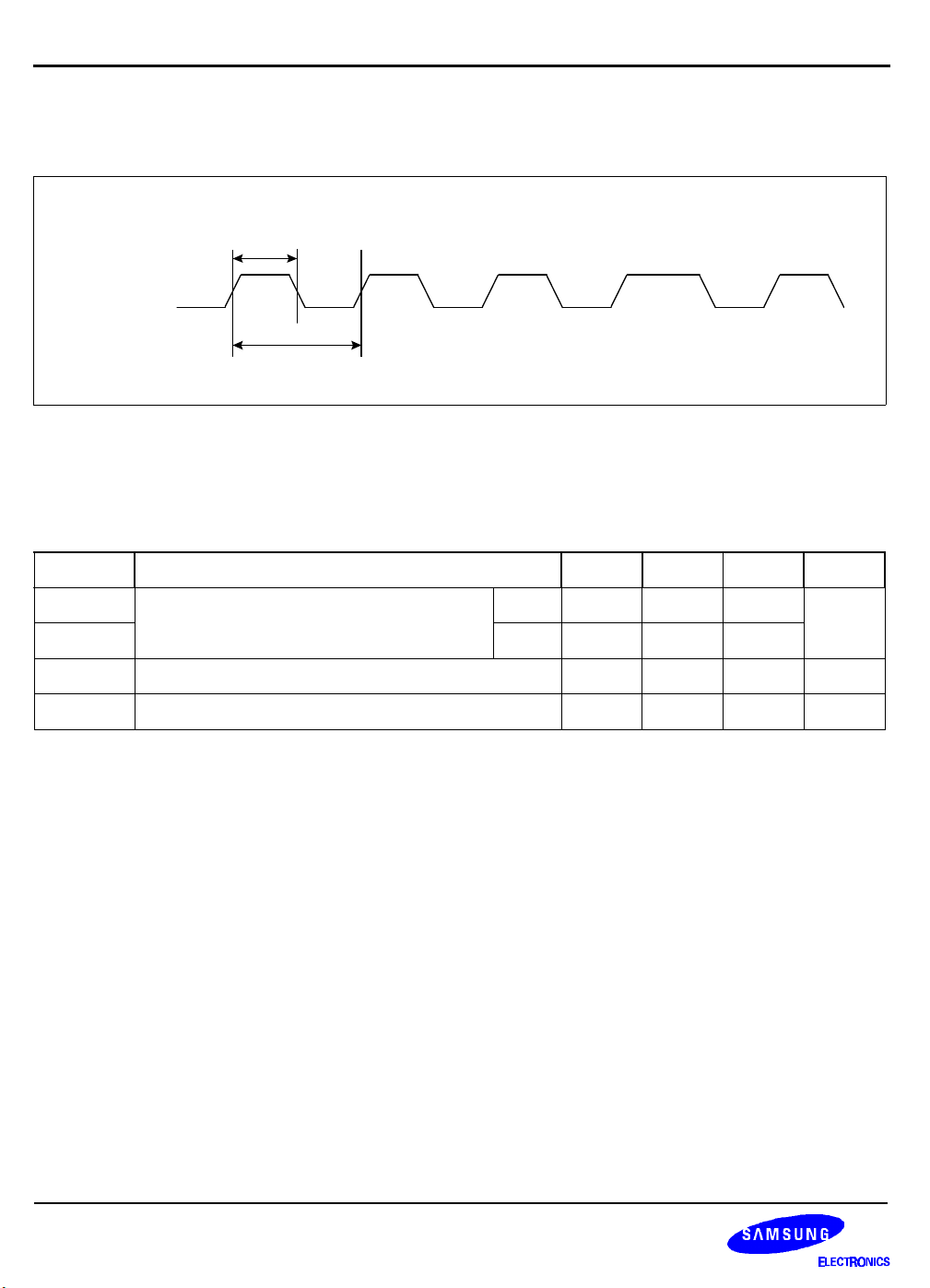
Preliminary Spec. ver 1.4
ELECTRICAL CHARACTERISTICS KS8910 100/10 Mbps ETHERNET TRANSCEIVER
MII-RECEIVE CLOCK TOLERANCE
t
1
RX_clk
t
2
Figure 8-3. MII-Receive Clock Tolerance Timing Diagram
Table 8-8. MII-Receive Clock Tolerance
Symbol Conditions Min Typ Max Unit
t1
100M 35 60 65
Rx_clk Duty Cycle
10M 35 50 65
t2a Rx_clk Period (100Base-TX / MII Interface) - 40 -
t2b Rx_clk Period (10Base-T / MII Interface) - 400 -
NOTES : 1.RX_clk Duty Cycle switching point is 50% if VDD
%
ns
ns
8-6
Page 78
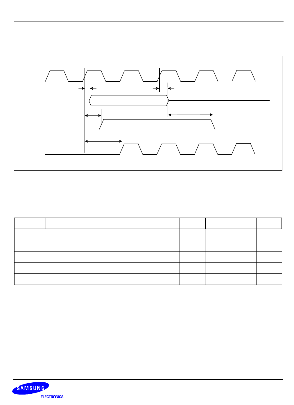
Preliminary Spec. ver 1.4
KS8910 100/10 Mbps ETHERNET TRANSCEIVER ELECTRICAL CHARACTERISTICS
MII/10BASE-T TRANSMIT TIMING
Tx_clk
TxD
t
1
t
2
Tx_en
Tx_er
t
3
t
4
CrS
t
5
TPOP
Figure 8-4. MII/10Base-T Transmit Timing Diagram
Table 8-9. MII/10Base-T Transmit Timing
Symbol Conditions Min Typ Max Unit
t1 TxD,Tx_en,Tx_er Setup to Tx-clk rise 10 - - ns
t2 TxD,Tx_en,Tx_er Hold from Tx-clk rise 10 - -
ns
t3 Tx_en sampled to CrS asserted - 4.8 -
t4 Tx_en sampled to CrS de-asserted - 2.0 -
t5 Tx_en sampled to TPO out (Tx latency) - 1.0 -
us
us
us
8-7
Page 79
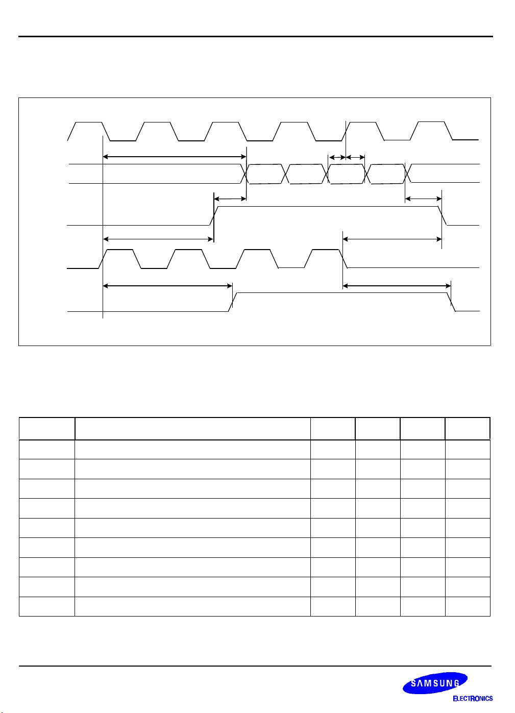
Preliminary Spec. ver 1.4
ELECTRICAL CHARACTERISTICS KS8910 100/10 Mbps ETHERNET TRANSCEIVER
MII/10BASE-T RECEIVE TIMING
Rx_clk
t
1
RxD
Rx_DV
Rx_er
t
4
CrS
t
6
TPIP
t
8
Col
Figure 8-5. MII/10Base-T Receive Timing Diagram
Table 8-10. MII/10Base-T Receive Timing
Symbol Conditions Min
t
t
2
3
t
5
t
7
t
9
Typ
Max
Unit
t1 TPI in to RxD out (Rx latency) - 4 - us
t2 RxD,Rx_DV,Rx_er Setup to Rx-clk rise 10 - -
t3 RxD,Rx_DV,Rx_er Hold form Rx-clk rise 10 - -
t4 CrS asserted to RxD,Rx_DV,Rx_er asserted - 0 -
t5 RxD,Rx_DV,Rx_er de-asserted to CRS de-asserted - 0 -
t6 TPIP in to CRS asserted 0 4 -
t7 TPIP quiet to CRS de-asserted 0 1.0 -
t8 TPIP in to COL asserted 0 1.7 -
t9 TPIP quiet to COL de-asserted 0 1.0 -
8-8
ns
ns
us
us
us
us
us
us
Page 80
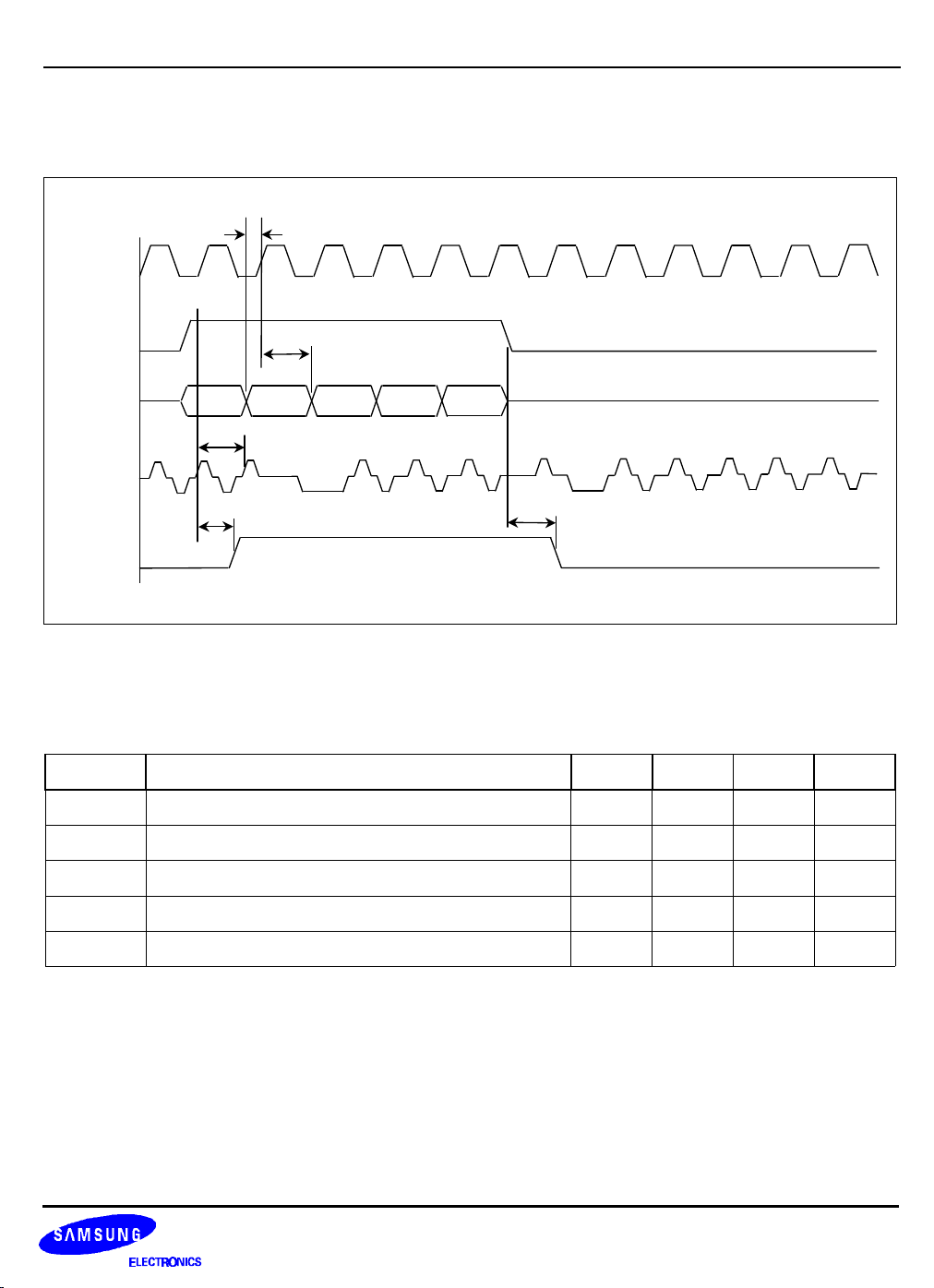
Preliminary Spec. ver 1.4
KS8910 100/10 Mbps ETHERNET TRANSCEIVER ELECTRICAL CHARACTERISTICS
MII/100BASE-TX TRANSMIT TIMING
t
1
Tx_clk
Tx_en
t
2
TxD[3:0]
t
3
TPOP
t
4
t
5
CrS
Figure 8-6. MII/100Base-TX Transmit Timing Diagram
Table 8-11. MII/100Base-TX Transmit Timing
Symbol Conditions Min Typ Max Unit
t1 TxD,Tx_en,Tx_er Setup to Tx-clk rise - - 25 ns
t2 TxD,Tx_en,Tx_er Hold from Tx-clk rise - - 25
ns
t3 Tx_en sampled toTPO out (Tx latency) - 50 -
t4 Tx_en sampled to CRS asserted - 10 -
t5 Tx_en sampled to CRS de-asserted - 50 -
ns
ns
ns
8-9
Page 81
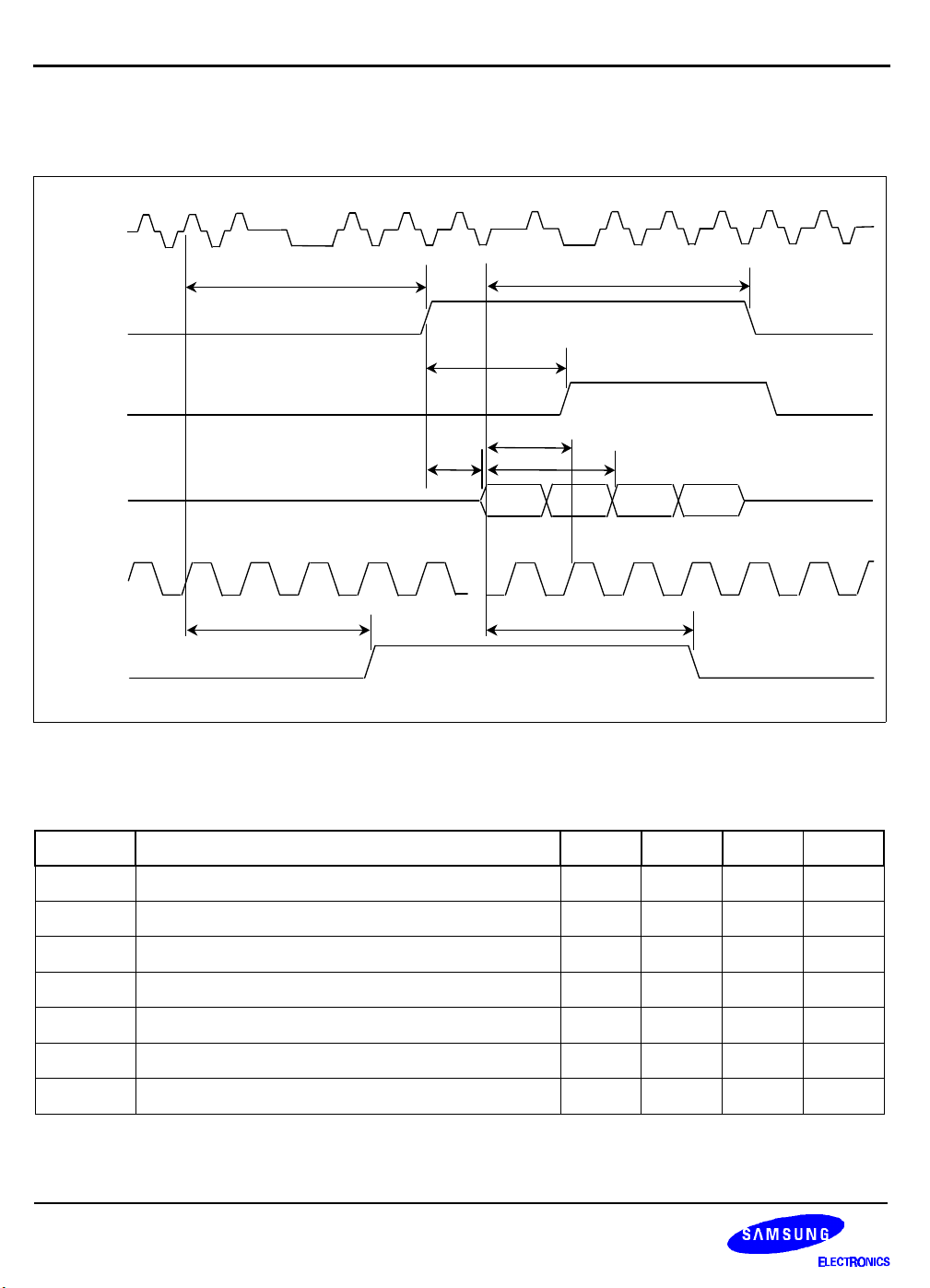
Preliminary Spec. ver 1.4
ELECTRICAL CHARACTERISTICS KS8910 100/10 Mbps ETHERNET TRANSCEIVER
MII/100BASE-TX RECEIVE TIMING
TPIP
CrS
RxDV
RxD[4:0]
Rx_clk
Col
t
6
t
4
t
t4 A
t
8
1
t
2
t
7
t
9
Figure 8-7. MII/100Base-TX Receive Timing Diagram
Table 8-12. MII/100Base-TX ReceiveTiming
Symbol Conditions Min Typ Max Unit
t1 RXD,RX_EN,RX_RX Setup to RX-CLK rise 10 - - ns
t2 RXD,RX_EN,RX_ER Hold from RX-CLK rise 10 - -
t4 CRS asserted to RX_DV asserted - 160 -
t6 Receive start of “J” to CRS asserted - 80 -
t7 Receive start of “T” to CRS de-asserted - 90 -
t8 Receive start of “J” to CRS asserted 0 15~19 20
t9 Receive start of “T” to CRS de-asserted 13 23~27 28
8-10
ns
ns
ns
ns
ns
ns
Page 82
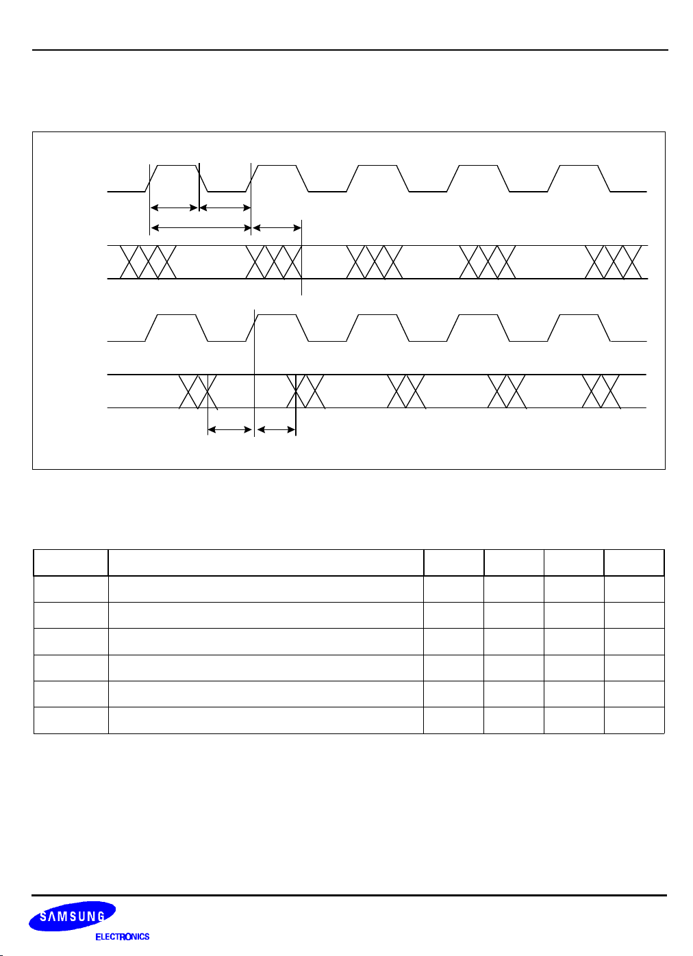
Preliminary Spec. ver 1.4
KS8910 100/10 Mbps ETHERNET TRANSCEIVER ELECTRICAL CHARACTERISTICS
MII-MANAGEMENT INTERFACE TIMING
MDC
t
1
t
2
t
3
t
4
MDIO
(output)
MDC
MDIO
(Input)
t
5
t
6
Figure 8-8. MII-Management Interface Timing Diagram
Table 8-13. MII-Management Interface Timing
Symbol Conditions Min Typ Max Unit
t1 MDC Minimum High Time 160 - - ns
t2 MDC Minimum Low Time 160 - -
t3 MDC Period 400 - -
t4 MDC rise to MDIO valid 0 - 300
t5 MDIO Setup to MDC 10 - -
t6 MDIO Hold after MDC 10 - -
ns
ns
ns
ns
ns
8-11
Page 83
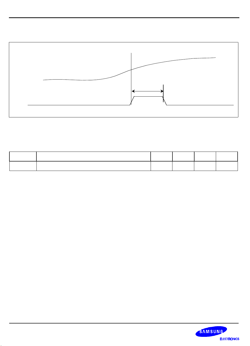
Preliminary Spec. ver 1.4
ELECTRICAL CHARACTERISTICS KS8910 100/10 Mbps ETHERNET TRANSCEIVER
POWER ON RESET TIMMING
VDD=2.0V
VDD
t
R
POR
Figure 8-9. Power On Reset Timming Diagram
Table 9-14. Power On Reset Timming
Symbol Conditions Min Typ Max Unit
tR Power_On to normal operation - 3.0 - us
8-12
Page 84
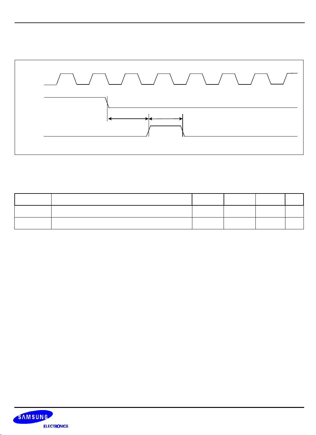
Preliminary Spec. ver 1.4
KS8910 100/10 Mbps ETHERNET TRANSCEIVER ELECTRICAL CHARACTERISTICS
10BASE-T SQE(Heartbeat) TIMING
Tx-clk
Tx_en
t
1
t
2
Ready
Figure 8-10. 10Base-T (SQE)Heartbeat Timing Diagram
Table 8-15. 10Base-T SQE(Heartbeat) Timing
Symbol Conditions Min Typ Max Unit
t1 COL(SQE) Delay after Tx_en off - 1.2 - us
t2 COL(SQE) Pulse duration - 1.2 - us
8-13
Page 85
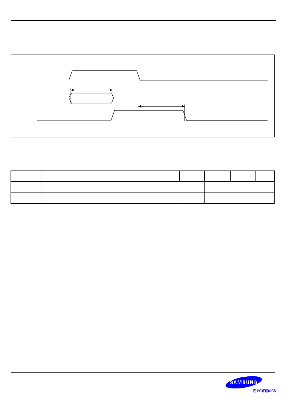
Preliminary Spec. ver 1.4
ELECTRICAL CHARACTERISTICS KS8910 100/10 Mbps ETHERNET TRANSCEIVER
10BASE-T JABBER TIMING
Tx_en
t
1
TxD
t
2
Col
Figure 8-11. 10Base-T Jabber Timing Diagram
Table 8-16. 10Base-T Jabber Timing
Symbol Conditions Min Typ Max Unit
t1 Maximum Transmit time - 100
2
- ms
t2 Unjab time - 500 - ms
8-14
Page 86
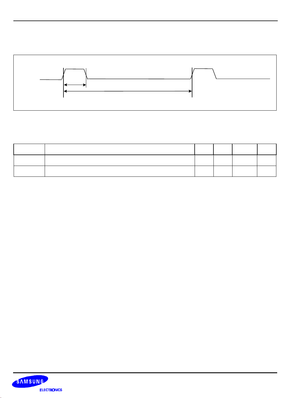
Preliminary Spec. ver 1.4
KS8910 100/10 Mbps ETHERNET TRANSCEIVER ELECTRICAL CHARACTERISTICS
10BASE-T NORMAL LINK PULSE TIMING
TPOP
t
1
t
2
Figure 8-12. 10Base-T Normal Link Pulse Timing Diagram
Table 8-17. 10Base-T Normal Link Pulse Timing
Symbol Conditions Min Typ Max Unit
t1 Normal Link Pulse Width (10Base-T) - 100 - ns
t2 COL Heartbeat assertion duration 8 10 24 ms
8-15
Page 87
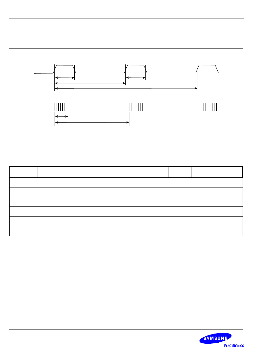
Preliminary Spec. ver 1.4
ELECTRICAL CHARACTERISTICS KS8910 100/10 Mbps ETHERNET TRANSCEIVER
AUTO- NEGOTIATION AND FAST LINK PULSE TIMING
Data Pulse Data Pulse
t
1
t
3
TPOP
TPOP
Clock Pulse
t
1
FLP Burst FLP Burst FLP Burst
t
4
t
2
t
5
Figure 8-13. Auto-Negotiation and Fast Link Pulse Timing Diagram
Table 8-18. 10Base-T Jabber Timing
Symbol Conditions Min
Typ
1
Max
t1 Clock/Data pulse width - 100 - ns
t2 Clock pulse to Data pulse timing - 64 - us
t3 Clock pulse to Clock pulse - 128 - us
Unit
t4 FLP Burst width - 2 - ms
t5 FLP burst to FLP burst timing 8 14 24 ms
t6 Number if Clock/Data pulses in a burst 17 - 33 pulses
8-16
Page 88
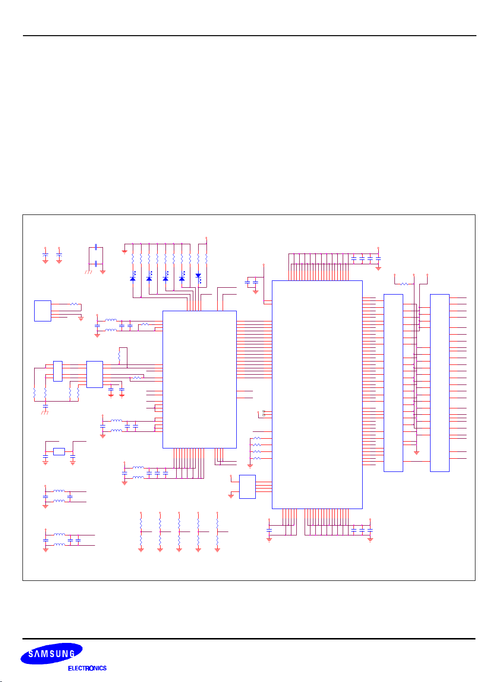
Preliminary Spec. ver 1.4
KS8910 100/10 Mbps ETHERNET TRANSCEIVER APPLICATION NOTE
9 APPLICATION NOTE
NIC APPLICATIONS
KS8920 MAC ETHERNET CONTROLLER APPLICATION
VddD1
2
R6
10
LED4
3VDD
VssD1
1
R7
§
330
RX
12
VddIO110VddIO239VddIO3
VddD247VssD2
48
SW5
0
SW10
0
3VDD
R9
R8
¥
¥
§
330
10
1 2
LED5
SPD
FDPLX
6
7
8
LEDR
LEDT5LEDL4LEDC3LEDS
FDPLX
U3
KS8910_64QFP
SubDIG
VssIO1
VssIO2
VssIO3
SubIO
57
9
40
54
55
56
3VDD
SW6
0
PDANEN SEL_7W
SW11
0
3VDD
R10
§
10
XTALOUT
XTALIN
11
12
XO
XI
TXCLK
TXD3
TXD2
TXD1
TXD0
TXEN
TXER
CRS
RXCLK
RXD3
RXD2
RXD1
RXD0
RXDV
RXER
MDC
MDIO
RESET
AN_EN
VddTXA
VssTXA
VssTXQ
VddTXQ
15
14
16
13
VDDTQ
VSSTQ
5VDD
3VDD
SW7
§
0
SW12
§
0
3VDD
19
16
14
8
C9
C10
§
§
0.1
0.1
63
COL
53
62
61
60
59
58
52
64
50
43
44
45
46
49
51
42
41
33
RST#
24
ANEN
3VDD
SEL_7W
§
R18 1.5
§
R19 1.5
§
R20 1.5
§
R21 1.5
8
4
VCC
DO
3
DI
2
SK
U4
1
5
CS
GND
93C46B
7
VSSIc
VSSIe
VDD3Ia4VSSIb6VDD3Ib
VDD3Ic11VSSId
36
VDD5ha
101
VDD5hc
110
COL
119
TXCLK
112
TXD3
113
TXD2
115
TXD1
116
TXD0
118
TXEN
121
TXER
109
CRS
126
RXCLK
3
RXD3
2
RXD2
1
RXD1
128
RXD0
124
RXDV
123
RXER
9
MDC
10
MDIO
KS8920_128QFP
107
LOOP_10
95
CAM_LOAD
94
CAM_HIT#
105
SEL_7W
106
LINK_10
103
SE
98
STM
5
TMS
88
PROM_DI
89
PROM_DO
91
PROM_CLK
92
PROM_CS
VDD3P1
VDD3P2
VDD3P3
VDD3O1
VSSO1
VSSP1
VSSP3
VSSP2
75
82
79
68
85
69
90
77
3VDD
C27
§
0.1
25
VDD3If
VDD3Ie21VSSIf23VDD3Id
VDD3O2
VSSO287VSSO3
96
93
28
31
VSSIg
VDD3lg
U1
VDD3O3
VSSO497VSSO5
99
43
34
VDD3lh
VDD3O4
102
100
49
VDD3Ii
VSSIi46VSSIh
VDD3O5
VSSO6
104
108
56
53
VDD3lk
VSSIj
VDD3O6
VSSO7
111
114
64
VDD3Ij
VSSIl
VDD3O7
VSSO8
120
61
VSSIa
VDD3O8
122
117
VDD3Il
VSSO9
125
72
127
C4
0.1
AD10
AD11
AD12
AD13
AD14
AD15
AD16
AD17
AD18
AD19
AD20
AD21
AD22
AD23
AD24
AD25
AD26
AD27
AD28
AD29
AD30
AD31
CBE#0
CBE#1
CBE#2
CBE#3
FRAME#
TRDY#
IRDY#
STOP#
DEVSEL
IDSEL
GNT#
REQ#
PERR#
SERR#
C28
0.1
C6
C5
C7
§
§
§
§
0.1
0.1
0.1
3VDD
PCIB1
86
AD0
AD0
45
84
AD1
AD1
AD2
AD3
AD4
AD5
AD6
AD7
AD8
AD9
PAR
INTA
CLK
RST#
AD1
AD2
83
43
81
AD3
AD3
80
AD4AD4
42
78
AD5
AD5
76
AD6
40
74
AD7
AD7
39
71
AD8
AD8
70
AD9
38
67
AD10
AD10
66
AD11
37
65
AD12
AD12
63
AD13
35
62
AD14
AD14
60
AD15
45
AD16
23
44
AD17
AD17
42
AD18
21
41
AD19
AD19
40
AD20
+3.3V
20
39
AD21
AD21
38
AD22
18
37
AD23
AD23
32
AD24
+3.3V
15
30
AD25
AD25
29
AD26
14
27
AD28
AD27
26
AD27
+3.3V
12
24
AD29
AD29
22
AD30
11
20
AD31
AD31
73
59
47
33
58
48
51
50
54
52
35
17
18
55
57
12
15
13
C29
§
0.1
+3.3V
CBE#0
CBE#1
CBE#134+3.3V
24
CBE#2
CBE#2
17
CBE#3
CBE#3
PAR
FRAME#
+3.3V
TRDY#
26
IRDY#
IRDY#
STOP#
28
DEVSEL
DEVSEL
IDSEL
PNT1#
GNT#
PNT2#
10
REQ#
REQ#
30
PERR#
PERR#
32
SERR#
SERR#
INTA
8
CLK
CLK
RST#
3VDD
C30
§
§
0.1
5VDD3VDD_2
SW1
§
0
1
GND
3
+5V
4
+5V
46
+5V
47
+5V
7
GND
9
GND
13
GND
16
19
GND
22
25
GND
27
29
GND
31
33
36
GND
41
44
GND
5
6
2
TDO
PCIA1
42
AD0
AD0
41
AD2
AD2
2
+5V
39
AD4
AD4
4
+5V
38
AD6
AD6
43
+5V
44
35
AD9
+5V
AD9
33
AD11
AD11
32
AD13
AD13
30
7
9
12
15
18
21
23
25
27
28
31
34
37
40
1
AD15
AD15
GND
20
AD16
AD16
+3.3V
19
AD18
AD18
GND
17
AD20
AD20
+3.3V
16
AD22
AD22
GND
13
AD24
AD24
+3.3V
11
AD26
AD26
GND
10
AD28
AD28
GND
8
AD30
AD30
+3.3V
36
CBE#0
CBE#0
GND
29
PAR
PAR
+3.3V
22
FRAME#
FRAME#
24
TRDY#
TRDY#
GND
26
STOP#
+3.3V
STOP#
14
IDSEL
GND
IDSEL
6
GNT#
GNT#
3
INTA
INTA
5
RST#
RST#
TDI
PCI Decoupling Caps Decoupling
3VDD
5VDD
C3
C2
§
§
22
22
5.0_3.3V POWER
U2
REG78R33
SW2
1
5VDD
+5V
+3.3V
GND
+5V
§
30
2
3VDD
3
4
5VDD
PHY Transceiver+ RJ45
J1
1
4
TX+
TXD+
5
TX-
TXD-2
3
RX+
8RXD+
7
6
RX-
RXD-
RJ-45
R1475R15
VDDDR
3VDD
3VDD
75
C40-2KV1
.001
XTALOUT
C19
17.5
C25
0.1
VDDTQ
C31
0.1
2
§
§
§
25Mhz
0.068
0.068
R16
75
XTALIN
X1
XI1XO
C20
17.5
L7
VDDDR
C26
L8
§
0.1
VSSDR
L9
C32
C33
0.068
L10
§
0.1
0.068
16
TX+
14
TX-
11
RX+
RX-9RD-
15
TXCT
10
RXCT
ST6122
R17
75
HALO
TG110-S131N2
VDDTQ
§
10
VSSTQ
C1
§
0.1
C8
§
0.1
3VDD
L1
0.068
C11
L2
§
0.1
0.068
T1
1
TD+
3
TD-
6
RD+
8
7
CT2
2
CT1
3VDD
C16
§
0.1
R1
R2
¥
§
330
10
LED1
LED2
COL
TX
12
§
C12
C13
25
R11
§
§
0.1
10
§
R12
200
TD+
TD- TPON
100
R13
RD+
TPOB
C15
C14
§
§
0.1
0.1
L3
VDDRQ
0.068
C18
C17
L4
§
§
0.1
10
VSSRQ
0.068
3VDD
L5
0.068
C21
L6
§
0.1
0.068
SW3
0
FDPLX SPSEL
SW8
0
§
TPOP
TPOB
TPIP
TPIN
SPSEL
PD
VDDDR
VSSDR
R4
R3
R5
§
¥
¥
10
330
330
LED3
LINK
12
12
28
VddRef
26
RB
27
VssRef
25
RBGND
21
TPOP
23
TPON
19
TPOB
32
TPIP
31
TPIN
29
SP_SEL
36
PD
18
VddDrv
17
VssDrv
20
SubDrv
22
VssDrv2
37
VddRxA
34
VddRxQ
30
SubAna
35
VssRxQ
38
VssRxA
VDDDIG
C22
C23
C24
§
§
§
10
0.1
0.1
VSSDIG
3VDD3VDD
SW4
0
SW9
0
Figure 10-1. KS8910(64-QFP-1414) Schematic Diagram with KS8920
9-1
Page 89

APPLICATION NOTE KS8910 100/10 Mbps ETHERNET TRANSCEIVER
Preliminary Spec. ver 1.4
MEMO
9-2
Page 90
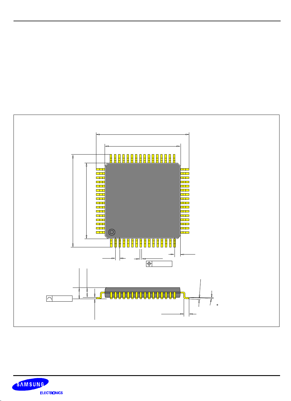
Preliminary Spec. ver 1.4
KS8910 100/10 Mbps ETHERNET TRANSCEIVER MECHANICAL DATA
10 MECHANICAL DATA
PACKAGE DIMENSION
64-QFP-1414 PACKAGE
0.10MAX
17.20 ± 0.30
14.00 ± 0.20
17.20 ± 0.30
14.00 ± 0.20
#64
#1
0.80
2.60 ± 0.10
2.80MAX
0.35 ± 0.10
0.10MAX
Demension in milimeter
1.00
0
5
1
0
.
.
0
0
-
+
5
1
.
0
0
~
8
0.80 ± 0.20
0.05MIN
Figure 10-1. KS8910 Package Dimension(64-QFP-1414 Type)
10-1
Page 91

Preliminary Spec. ver 1.4
MECHANICAL DATA KS8910 100/10 Mbps ETHERNET TRANSCEIVER
MEMO
10-2
Page 92

Preliminary Spec. ver 1.4
KS8910 100/10 Mbps ETHERNET TRANSCEIVER APPENDIX
11 APPENDIX
GLOSSARY
This glossary contains a brief explanation of technical terms, abbreviations, and acronyms used in this document.
ETHERNET AND NETWORKING ACRONYMS AND TERMS
• 10BASE5 - 500-meter-per-segment Ethernet using half-inch diameter thick coaxial cable. Up to 100 nodes.
• 10BASE2 - 185-meter-per-segment Ethernet, using RG-58 50-ohm thin coaxial cable similar to that used for
community-antenna television. Up to 30 nodes. Also, Cheapernet or Thinnet.
• 10BASE-T - 24-gauge, unshielded, twisted-pair 10-Mbit/s Ethernet.
• 100BASE-FX - 100-Mbit/s Ethernet using fibre optic cable.
• 100BASE-T - Twisted-pair 100-Mbit/s Fast Ethernet, over one of the following media: 100BASE-TX, 100BASEFX, 100BASE-T4, or 100BASE-T2.
• 100BASE-T2 - 100-Mbit/s Ethernet using two pairs of Category-3, 4, or 5 generic twisted balanced cable.
• 100BASE-T4 - 100-Mbit/s Ethernet using four pairs of Category-3, 4, or 5 generic twisted balanced cable.
• 100BASE-TX - 100-Mbit/s Ethernet using two pairs of Category-5 balanced cable or 150 Ohm sielded
balanced cable.
• 100BASE-X - 100-Mbit/s Ethernet 100BASE-TX or 100BASE-FX.
• 100BASE-VG - IEEE 802.12 Network Protocol. See AnyLAN.
• AnyLAN - Also 100BASE-VG AnyLAN.100-Mbit/s alternative to Ethernet and Token Ring. Also, IEEE 802.12.
• ADSL - Asymmetric Digital Subscriber Lines. From Bell Communications Research Inc. Uses as few as fourwire twisted pair.
• Alignment error - When the Mac receives a frame that is not an integer number of bytes long, and the CRC is
invalid. Synonym: framing error. See also, dribble.
• ARP - Address Resolution Protocol. Maps an Internet address to a physical address. Not all networks need it.
• AUI - Attachment Unit Interface layer of LAN CSMA/CD. Connects the DTE to the MAU. See OSI. Used with
thick Ethernet, involving a drop cable.
• Babble - Transmit continuously for more than 1500 bytes.
• Big endian - The byte at memory address 0 contains the most-significant bits. Used by IBM 370, Motorola
68000, Pyramid, and TCP/IP protocol header integers.
• Bridge - A store-and-forward device connecting physical networks that merely passes all packets. Unlike a
gateway, strictly speaking, it performs no protocol conversion, and unlike a router, it does not switch packets to
the appropriate network (although some bridges can learn where various hosts reside and route packets).
• Broadcast address - A distinguished, predefined multicast address that always denotes the set of all stations
on a given local area network. All ones in the destination address field shall be predefined to be the broadcast
A-1
Page 93

Preliminary Spec. ver 1.4
APPENDIX KS8910 100/10 Mbps ETHERNET TRANSCEIVER
address, ff-ff-ff-ff-ff-ff.
• Bundle - A group of signals which have a common set of characteristics and differ only in their information
content.
• Capture effect - Under heavy load, if at least one of the contending stations is capable of transmitting back-toback packets continuously, that station can capture the network for long periods. This occurs because, once a
station has succeeded in transmitting, it zeroes its attempts counter, so its next maxBackOff will be set to 2.
Other stations, however, will continue to increment their attempts counters, causing their maxBackOff variables
to grow exponentially. The network still carries traffic at its full rate (except for second-order effects), but its
arbitration has become unfair.
• CCITT - Consultative Committee for International Telephony and Telegraphy. Renamed ITU.
• Cheapernet - 185-meter-per-segment Ethernet. Also, 10BASE2.
• CSMA/CD - Carrier Sense Multiple Access with Collision Detection. Used by Ethernet.
• CDDI - Copper Distributed Data Interface. FDDI without the fiber.
• CO - Central Office.
• CRC - Cyclic Redundancy Code. Called Cyclic Redundancy Check in IEEE 802.3 document.
• DCE - Data Communications Equipment.
• DS0 - 64-Kbit/s asynchronous rate. One voice channel.
• DS1 - 1.544 Mbit/s asynchronous rate. 24 DS0 signals. T1 equipment and cable carry DS1 rate and format
between COs.
• DS2 - 6.312 Mbit/s asynchronous rate. Four DS1 signals.
• DS3 - 44.736 Mbit/s asynchronous rate. 28 DS1 signals. T3 equipment and cable carry DS3 rate and format
between COs.
• DMA - Direct Memory Access.
• Dribble - When the Mac receives a frame that is not an integer number of bytes long. Dribble produces an
alignment error when the CRC is invalid.
• DTE - Data Terminal Equipment. If the AUI is not exposed, this is the PLS and up. See OSI.
• EFD - The End of Frame Delimiter <EFD> indicates the end of a transmission. For the MII, deassertion of the
Tx_en signal constitutes an end of frame delimiter.
• Fast Ethernet group - 100-Mbit/s CSMA/CD Ethernet proposal C.f. 100BASE-VG or AnyLAN. Supported by
approximately 30 companies, including Grand Junction Networks Inc., Sun Microsystems Inc., 3Com corp.,
Cabletron Systems Inc., and Synoptics Communications Inc.
• FCS - Frame Check Sequence. Also, CRC.
• FDDI - Fiber Distributed Data Interface. Fiber-optic Data Distribution Interface. 100 Mbit/s.
• FIFO - First-In, First-Out data buffer. Also, silo or queue.
• Fragment - A frame that is less than 64 bytes (minFrameSize) long, exclusive of preamble and SFD. Presumed
to be the result of a collision, fragments are discarded and are not reported as an error. Also, runt packet.
• Frame - A frame is everything in a packet except the preamble and the start frame delimiter: destination and
source addresses, length, LLC data, padding, and frame check sequence.
• Framing error - See alignment error, dribble.
• Gateway - A device connecting networks that performs some protocol conversion.
A-2
Page 94

Preliminary Spec. ver 1.4
KS8910 100/10 Mbps ETHERNET TRANSCEIVER APPENDIX
• Globally administered address - An Ethernet address whose second bit transmitted, used to distinguish
between locally or globally administered addresses, is set to 0, indicating a globally administered (or U,
universal) address. If an address is to be assigned locally, this bit is set to 1. Note that for the broadcast
address, this bit is also a 1.
• Group address - An Ethernet destination address whose first bit transmitted, used to identify it either as an
individual or as a group address, is 1, indicating that the address field contains a group address that identifies
none, one or more, or all of the stations connected to the local area network. More commonly called a multicast
address. The first byte of a multicast address is odd, for example, 01-00-00-00-00-00. There are two kinds of
multicast address: (a) Multicast-group address. An address associated by higher-level convention with a group
of logically-related stations. (b) Broadcast address. A distinguished, predefined multicast address, ff-ff-ff-ff-ff-ff,
that always denotes the set of all stations on a given local area network.
• HDLC - High-level Data Link Control. Used in X.25.
• Heartbeat - Signal Quality Error (SQE).
• IAB - Internet Activities Board.
• ICMP - Internet Control Message Protocol. The protocol to handle error and control information between
gateways and hosts. TCP/IP networking software, not user processes, generates and processes ICMP
messages.
• IEEE 1149.1 - See JTAG.
• IEEE 802.12 - 100-Mbit/s standard based on demand priority. Also, 100BASE-VG or AnyLAN.
• IEEE 802.3 - Information technology Local and metropolitan area networks Part 3: Carrier sense multiple
access with collision detection (CSMA/CD) access method and physical layer specifications. International
Standard ISO/IEC 8802-3: 1993(E), ANSI/IEEE Std. 802.3, 1993 Edition, July 8, 1993. Also, Ethernet.
• IEEE 802.4 - Token bus.
• IEEE 802.5 - Token ring.
• Individual address - An Ethernet address whose first bit transmitted, used to identify it either as an individual or
as a group address, is 0, indicating that the address field contains an individual address, and so is associated
with a particular station on the network. The first byte of a individual address is even, for example, 00-00-00-0000-00.
• IP - Internet Protocol. Fragments (segments), routes, delivers, and reassembles packets for TCP, UDP, and
ICMP. Connectionless and unreliable. Adds a 20-byte header and a check sum.
• ISDN - Integrated Services Digital Network.
• ISO - International Organization for Standardization.
• Jabber - In order to protect the network from babbling nodes, IEEE Std. 803.3 requires MAUs to inhibit
transmission onto the network if they have been transmitting for an excessive time. The window for jabber must
be between 20 and 150 ms.
1
• JTAG - Joint Test Action Group. A group of companies that developed what became IEEE 1149.1 Test Access
Port... for board-level production test of integrated-circuit pin continuity.
1. Project 802 Local and Metropolitan Area Networks. Draft Guide to ANSI/IEEE Std. 802.3 (CSMA/CS Ac-
cess Method and Physical Layer Specifications). SysTAG Network Guide, Draft 5.2, January 23, 1994.
Section 3.5 False Jabber, page 13.
A-3
Page 95

Preliminary Spec. ver 1.4
APPENDIX KS8910 100/10 Mbps ETHERNET TRANSCEIVER
• LAN - Local Area Network.
• Little endian - The byte at memory address 0 contains the least-significant bits. Used by Intel x86, DEC Vax,
and DEC PDP-11.
• LLC - Logical Link Control layer of LAN CSMA/CD. The upper half of the OSI (which see) reference model data
link layer, between the MAC and the network layer.
• Locally administered address - An Ethernet address whose second bit transmitted, used to distinguish between
locally or globally administered addresses, is set to 1, indicating a locally administered address. If an address is
to be assigned globally (or U, universal), this bit shall be set to 0. Note that for the broadcast address, this bit is
also a 1.
1
• MAC - Media Access Control layer of LAN CSMA/CD. The lower half of the OSI (which see) reference model
data link layer, between the LLC and the PLS.
• MAU - Medium Attachment Unit layer of LAN CSMA/CD. See OSI.
• MDI - Medium Dependent Interface layer of LAN CSMA/CD. The part of the MAU that connects the PMA to the
medium. See OSI.
• MII - Media Independent Interface. A four-bit-wide interface between a reconciliation layer and the PLS. The
reconciliation layer connects to the MAC using the existing 802.3 MAC-PLS interface.
• Minimum frame length - 64 bytes (512 bits). Note that this does not include the preamble and the start frame
delimiter.
• Multicast address - An Ethernet destination address whose first bit transmitted, used to identify it either as an
individual or as a group address, is 1, indicating that the address field contains a group address that identifies
none, one or more, or all of the stations connected to the local area network. The first byte of a multicast
address is odd, for example, 01-00-00-00-00-00. There are two kinds of multicast address: (a) Multicast-group
address. An address associated by higher-level convention with a group of logically-related stations. (b)
Broadcast address. A distinguished, predefined multicast address that always denotes the set of all stations on
a given local area network.
• Multicast-group address - An address associated by higher-level convention with a group of logically-related
stations. This is one of two kinds of multicast address, the other being the broadcast address, ff-ff-ff-ff-ff-ff.
• NDIS - Network Driver Interface Specification for a generic device driver, independent of protocol or hardware.
• Network acquisition time - If the DTE transmits for a period exceeding the net acquisition time without detecting
a collision, then the DTE is said to have acquired the network. The DTE will send the remainder of its frame
without the possibility of having a collision in a correctly operating network. By this time, all DTEs in the network
have detected network activity and are deferring to it.... For example, the network acquisition time on a single-
segment 10BASE5 network of 500-meter length is approximately 108 bit times.2 Also called round trip delay.
• NIC - Network Interface Controller or Card. Also Network Information Center, at SRI International, which
assigns a network a class field (A, B, or C) and a unique network ID field of the 32-bit TCP/IP addresses.
• OC1 - 51.84 Mbit/s Optical Carrier 1, SONET Synchronous Transport Signal STS-1. 28 DS1 signals or one
DS3.
• OC3 - 155.52 Mbit/s Optical Carrier 3, SONET Synchronous Transport Signal STS-3. Three byte-interleaved
STS-1 signals.
1. ANSI/IEEE Std. 802.3, 1993 Edition. Section 3.2.3 Address Fields, page 42.
2. Project 802 Local and Metropolitan Area Networks. Draft Guide to ANSI/IEEE Std. 802.3 (CSMA/CS Ac-
cess Method and Physical Layer Specifications). SysTAG Network Guide, Draft 5.2, January 23, 1994.
Section 2.3.1: Network Acquisition Time, page 4.
A-4
Page 96

Preliminary Spec. ver 1.4
KS8910 100/10 Mbps ETHERNET TRANSCEIVER APPENDIX
• OC12 - 622.08 Mbit/s Optical Carrier 12, SONET Synchronous Transport Signal STS-12. Twelve byteinterleaved STS-1 signals.
• OC48 - 2488.32 Mbit/s Optical Carrier 48, SONET Synchronous Transport Signal STS-48. 48 byte-interleaved
STS-1 signals.
• Octet - byte.
• OSI - Open System Interconnection reference model layers adopted by the ISO application, presentation,
session, transport, network, data link (composed of LLC and MAC layers of LAN CSMA/CD), and physical
(composed of PLS and PMA layers of LAN CSMA/CD, connected by AUI). Also, Obsolete Systems
Interconnect.
1
• Packet - According to 802.3 Tutorial, a packet is a frame, preceded by the preamble and the start frame
delimiter fields. Thus, it consists of (1) preamble, (2) start frame delimiter, (3) destination and (4) source
addresses, (5) length, (6) LLC data, (7) padding, and (8) frame check sequence fields.
• PCI - Peripheral Component Interconnect. 32 or 64 bits wide, 0 to 33 MHz clock rate, 132 to 264 MBytes/s
(peak). Intel Corporation released version 1.0 of the PCI specification on June 22, 1992, and the PCI Special
Interest Group released revision 2.0 on April 30, 1993.
• Ping - Packet InterNet Groper. Tests the reachability of another site by sending an ICMP echo request
message.
• PCMCIA - Personal Computer Memory Card International Association. Also, People Can’t Memorize Computer
Industry Acronyms.
• PDU - Protocol Data Unit in ATM.
• PHY - Physical Layer Entity, as defined in the 802 Architecture and Overview Standard. The word PHY is used
to denote the set of functions associated with a physical layer protocol.
• PLS - Physical Signalling layer of LAN CSMA/CD. See OSI.
• PMA - Physical Medium Attachment. See OSI.
• PMD - Physical Medium Dependent layer. PMD connects to MAC via MII on one side, and connects to MDI on
the other.
• PPP - Point-to-Point Protocol. Successor to SLIP, Serial Line Internet Protocol. Provides router-to-router and
host-to-network connections over both synchronous and asynchronous circuits.
• PSTN - Public Switched Telephone Network.
• Preamble - The first field of a packet, up to seven bytes long. Each byte has value 10101010, transmitted left to
right.
• QAM - Quadrature Amplitude Modulation. Modulation of both amplitude and phase, to increase the information
capacity of a channel.
• RARP - Reverse Address Resolution Protocol. Maps a physical address to an Internet address. Only some
networks need it.
• Repeater - Connects two or more Ethernet segments, with signal amplification and timing and preamble
regeneration, but without storing packets.
• RJ-11 - Four-wire modular telephone connector.
• RJ-45 - Eight-wire modular telephone connector.
1. Greg Chesson, “ Protocol Engine Design”, Summer Usenix Conference, Phoenix Arizona, 1987, pages
209-215.
A-5
Page 97

Preliminary Spec. ver 1.4
APPENDIX KS8910 100/10 Mbps ETHERNET TRANSCEIVER
• Router - A store-and-forward protocol-dependent device connecting networks that switches packets to the
appropriate network.
• Runt - A frame that is less than 64 bytes (minFrameSize) long, exclusive of preamble and SFD. Synonym:
fragment.
• Saturn - Sonet-ATM User Network. A group to develop chips to Sonet and ATM Forum specifications.
• SCSI - Small Computer System Interface.
• SDH - Synchronous Digital Hierarchy. ITU’s European designation for fiber-optic transmission. See also Sonet.
• SDLC - Synchronous Data Link Control. Used in Systems Network Architecture.
• Sending End Overshoot SEO.
1
• SFD - Start Frame Delimiter. A single byte with value 10101011, transmitted from left to right. It follows the
preamble.
• Signal Quality Error - SQE. Also, heartbeat.
• SLIP - Serial Line Internet Protocol. Predecessor to PPP.
• SMDS - Switched Multimegabit Data Service, a 45-Mbit/s cell-relay service based on IEEE 802.6 Distributed
Queue Dual Bus. Also, Sorta Mega Data Stuff. (Seen on a workbench at Pacific Bell s Broadband Labs,
Concord, California.)
• SMTP - Simple Mail Transfer Protocol. An application program provided by almost every TCP/IP
implementation.
• SNMP - Simple Network Management Protocol. Allows a TCP/IP host to query other nodes for network-related
statistics and error conditions.
• Sonet - Synchronous Optical Network. ANSI U.S. fiber-optic transmission standard. See also SDH.
• SonicTM - National Semiconductor Corporation’s DP83932B Systems-Oriented Network Interface Controller.
• Spanning tree - An algorithm to create a logical topology connecting all network segments, and ensures that
only one path exists between any two stations.
• Spool - Simultaneous Peripheral Operation On-line.
• SQE - Signal Quality Error. Also, heartbeat.
• Start Frame Delimiter - see SFD.
• Station address - An Ethernet address whose first bit transmitted, used to identify it either as an individual or as
a group address, is 0, indicating that the address field contains an individual address, and so is associated with
a particular station on the network. The first byte of a multicast address is even, for example, 00-00-00-00-00-
00.
• STS-1 - Synchronous Transport Signals.
• T1 - 1.544 Mbits/s.
• TAP - Test Access Port. See JTAG.
1. Project 802 Local and Metropolitan Area Networks. Draft Guide to ANSI/IEEE Std. 802.3 (CSMA/CS Ac-
cess Method and Physical Layer Specifications). SysTAG Network Guide, Draft 5.2, January 23, 1994.
Section 4.9: Sending End Overshoot (SEO), page 33.
A-6
Page 98

Preliminary Spec. ver 1.4
KS8910 100/10 Mbps ETHERNET TRANSCEIVER APPENDIX
• TCP - Transmission Control Protocol, a connection-oriented, reliable, full-duplex, virtual circuit byte-stream
facility for a user process. Uses IP. Part of the TCP/IP protocol suite.
• TCP/IP - Transmission Control Protocol/Internet Protocol, the DARPA Internet protocol suite.
• Type 1 cable - Shielded, two-pair cable.
• Type 3 cable - Unshielded, twisted-pair cable.
• UDP - User Datagram Protocol, a connectionless, unreliable datagram facility for a user process. Uses IP. Part
of the TCP/IP protocol suite.
• Universal address - An Ethernet address whose second bit transmitted, used to distinguish between locally or
globally administered addresses, is set to 0, indicating a globally administered (or U, universal) address. If an
address is to be assigned locally, this bit shall be set to 1. Note that for the broadcast address, this bit is also a
1
1.
• V.32terbo modem - 19.2 Kbits/s.
• V.34 modem - 28.8 Kbits/s.
• VESA - Video Electronics Standards Association, an association of companies involved in the design and
manufacture of video graphics adapters.
• VL - VESA Local bus.
1. ANSI/IEEE Std. 802.3, 1993 Edition. Section 3.2.3 Address Fields, page 42.
A-7
Page 99

Preliminary Spec. ver 1.4
APPENDIX KS8910 100/10 Mbps ETHERNET TRANSCEIVER
NOTES
A-8
 Loading...