

Samsung KS16114 Datasheet

KS16112/4
9600/14400 bps FAX MODEM
INTRODUCTION
The KS16112 and KS16114 are synchronous, half - duplex
modems capable of speeds up to 9600 bps ( KS16112 ) or
up to 14400 bps ( KS16114 ).
These modem devices can operate over the public switched
telephone network ( PSTN ) with the addition of the appropriate
data access arrangement ( DAA ).
These modems satisfy the requirements specified in ITU-T re commendations V.17 ( KS16114 ), V.29, V.27 ter, V.21 Channel 2
and T.4, and meet the binary signaling requirements of T.30.
These products are intended to be used in
Group 3 facsimile machines or fax processing boards
and can operate at 14400 ( KS16114 ), 12000
( KS16114 ), 9600, 7200, 4800, 2400 or 300 bps
depending on the selected configuration.
These devices also feature V.17 short train
( KS16114 ) and V.27 ter short train and three
programmable tone detectors as well as a pro grammable DTMF receiver. Additionally, HDLC
framing ( according to T.30 ) at 14400 ( KS16114 ),
12000 ( KS16114 ), 9600, 7200, 4800, 2400 or 300 bps
is also featured.
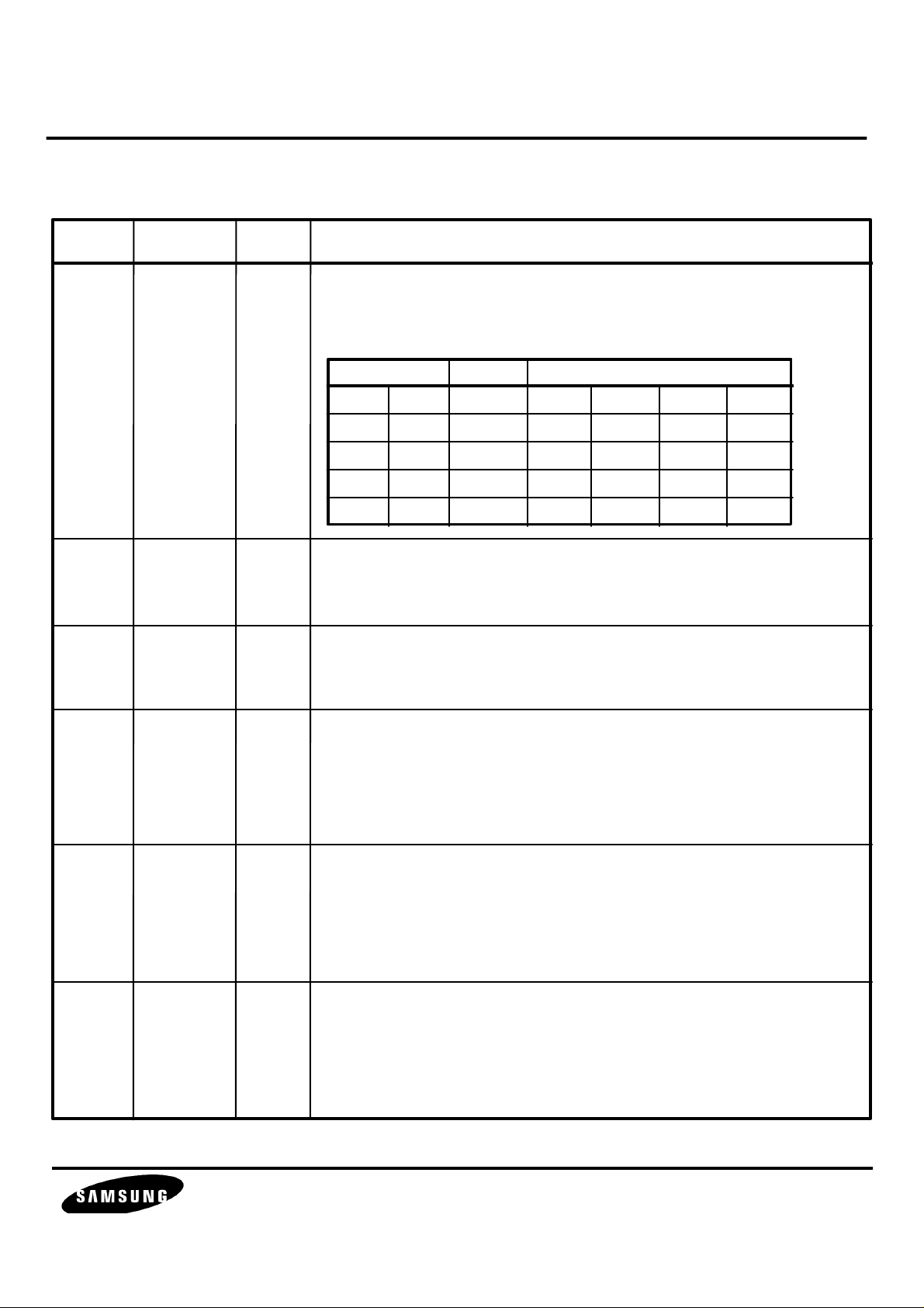
ORDERING INFORMATION
Device Package
KS16112
KS16114
68 - PLCC - SQ
KS16112/4
Operating Temperature
68-PLCC-SQ
0 ~ +70 °C
68-PLCC-SQ
FEATURES
• Group 3 facsimile transmission / reception according to :
- ITU-T V.17 short and long train ( KS16114 )
- ITU-T V.29, V.27 ter short and long train, V.21 Ch.2, T.30 and T.4
• Half - duplex operation
• Receiver dynamic range : 0 dBm to - 43 dBm
• Programmable transmit level : 0 dBm to - 15 dBm
• Programmable dual tone generation
• Programmable tone detection
• Programmable interface memory interrupt
• Programmable turn on and turn off thresholds
• Automatic T/ 2 adaptive equalizer
• HDLC capability at all speeds
• Diagnostic capability allowing telephone line quality monitoring
• ITU-T V.24 compatible interface
• TTL and CMOS compatible
• Low power consumption, KS16112 : 400mW typical, KS16114 : 550mW typical
• Programmable compromise filter for high speed RX modes
- 1 -
KS16112/4
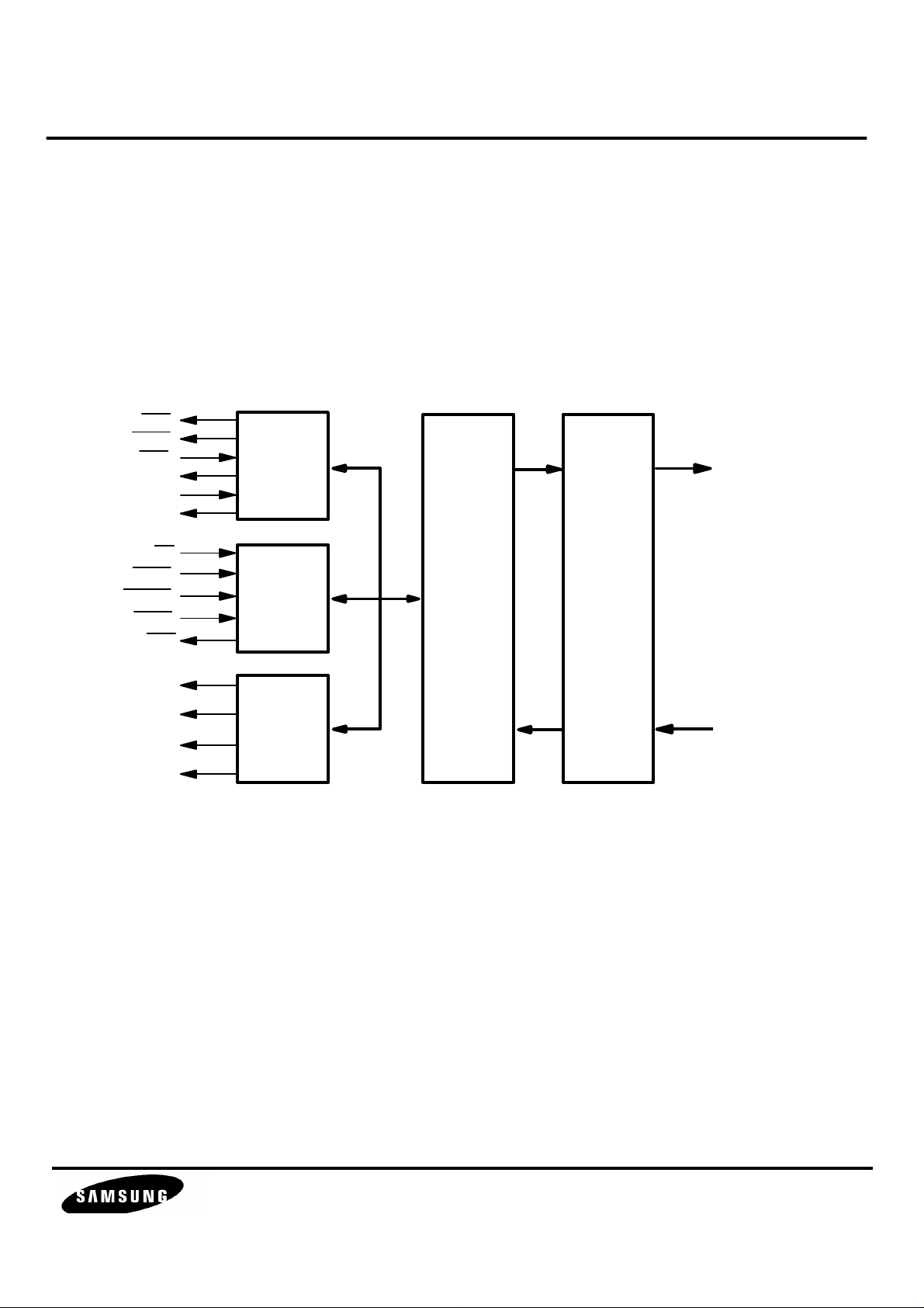
BLOCK DIAGRAM
9600/14400 bps FAX MODEM
CTS
RLSD
RTS
DCLK
TXDI
RXDO
CS
READ
WRITE
EN85
IRQ
SEPWCLK
SEPCLK
SEPXO
SEPYO
V.24 I/F
&
Timing
Chain
Host I/F
&
Dual - port
RAM
Eye
Pattern
I/F
Digital
Signal
Processor
TXAO
Analog
Front
End
RXAI
- 2 -
KS16112/4
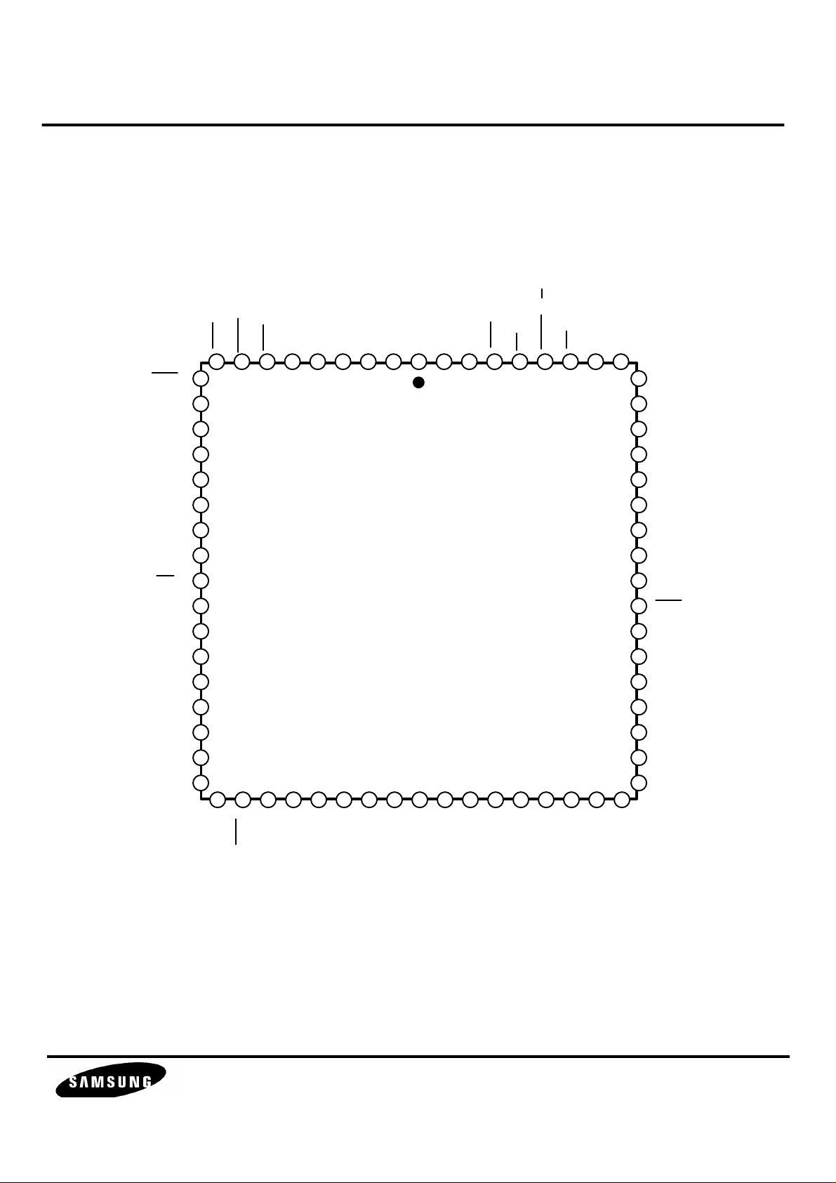
PIN CONFIGURATION
EN85
PORI
10
9600/14400 bps FAX MODEM
EN85I
RTS
NC
NC
RS0
RS1
RS2
RS3
GNDD1
RS4
READ - Ø2
CS
WRITE - R/W
IRQ
D0
D1
9 8 7 6 5 4 3 2 1 68 67 66 65 64 63 62 61
60
D2
XTALI
XTALO
XCLKO
YCLKO
V
DD
DCLKI
SYNCIN2
CTS
TXDI
DCLK
SEPWCLK
SEPCLK
SEPXO
ADIN
DAOUT
SEPYO
11
12
13
14
15
16
17
18
19
20
21
22
23
24
25
26
27 28 29 30 31 32 33 34 35 36 37 38 39 40 41 42 43
KS16112 / 4
59
58
57
56
55
54
53
52
51
50
49
48
47
46
45
44
D3
D4
D5
D6
D7
GNDD2
AGCIN
GNDA1
PORO
RCI
SYNCIN1
DAIN
ADOUT
ECLKIN2
RXAI
AOUT
RXDO
RLSD
RCVO
GNDA2
VBB AUXAI
FOUT
TXAO
AES
- 3 -
AEE
NC
ECLKIN
VCC
CABL1
CABL2
RCVI
FIN

KS16112/4
PIN DESCRIPTION
9600/14400 bps FAX MODEM
Pin No. Symbol
67
1
2
3
4
55
56
57
58
59
60
61
62
65
RS4
RS3
RS2
RS1
RS0
D7
D6
D5
D4
D3
D2
D1
D0
CS
Type
I
I/O
I
Description
• Register select bus
These lines are used to address interface memory registers within
the modem. When CS is active, the modem decodes RS0 through
RS4 to address one of its 32 internal interface memory registers.
RS4 is the most significant bit. In a typical design, RS0 - RS4 are
connected to A0 - A4 address lines of the host microprocessor.
• Data bus
These bi-directional data bus lines provide parallel data transfer
between the modem and the host microprocessor.
D7 is the most significant bit.
The direction of the D0 - D7 data bus is controlled by the
READ - Ø2 and WRITE - R/W signals.
When not being written into or read from, D0 - D7 assume the
high impedance state.
• Chip select
The modem is selected and decodes RS0 - RS4 when CS
becomes active at which time data transfer between the modem
and the host can take place over the parallel data bus.
Typically, CS is driven by address decode logic.
66
64
READ - Ø2
WRITE -R/W
• Read enable ( bus mode ) or phase2 ( 6500 bus mode )
If 8085 bus mode is selected ( EN85 is connected to ground ), this
I
I
signal acts as the READ input.
If 6500 bus mode is selected ( EN85 is pulled - up to +5V ), this signal
acts as the Phase 2 clock input.
• Write enable ( bus mode ) or R/W ( 6500 bus mode )
If 8085 bus mode is selected ( EN85 is connected to ground ), this
signal acts as the WRITE input.
If 6500 bus mode is selected ( EN85 is pulled - up to +5V ), this signal
acts as the R/W strobe.
- 4 -
KS16112/4
PIN DESCRIPTION ( Continued )
9600/14400 bps FAX MODEM
Pin No.
63
19
27
Symbol
IRQ
TXDI
RXDO
Type
O
I
O
Description
• Interrupt request
The modem can use IRQ to interrupt the host microprocessor
program execution. IRQ can be enabled in the modem interface
memory to be asserted in response to a specified change of
conditions in the modem status. IRQ is an open drain output
and must be connected to an external pull up resistor of suitable
value ( typically, a 5.6 KΩ, 1/4 watt, 5% resistor is adequate ).
• Transmit data input
TXDI is the modem’s transmit data serial input. When configured for
serial data mode ( PDME bit is reset ) the modem accepts data bits
for transmission via this input. When transmitting data, the modem reads
the TXDI pin on the rising edge of DCLK. When the modem is con figured for parallel data mode ( PDME bit is set ), the TXDI pin is ig nored and transmit data is accepted by the modem via the DBFR register.
• Receive data output
RXDO is the modem receive data output.
Received data is output to the DTE via the RXDO pin in both
serial and parallel data modes ( PDME bit set or reset ).
When receiving data, the modem outputs a data bit on the falling
edge of DCLK.
The center of RXDO bits coincides with the rising edge of DCLK,
thus, the DTE should read RXDO on the rising edge of DCLK.
• Request to send
When the RTS input is forced low, the transmitter starts transmitting
the modem training sequence according to the selected configuration.
Once the training sequence has been transmitted ( signaled by the
7
RTS
I
CTS pin and CTSB bit becoming active ), data present at either the
TXDI input pin in serial mode ( PDME bit is reset ) or written into the
DBFR register in parallel mode ( PDME bit is set ) is modulated and
transmitted.
The RTS input pin is logically ORed with the RTSB bit in the
interface memory.
- 5 -
KS16112/4
PIN DESCRIPTION ( Continued )
9600/14400 bps FAX MODEM
Pin No. Symbol
18
28
20
CTS
RLSD
DCLK
Type
O
O
O
Description
• Clear to send
CTS is used to indicate of that the training sequence transmission
has been completed and the modem is ready to transmit any
data present at either the TXDI input pin in serial mode
( PDME bit is reset ) or in DBFR in parallel mode ( PDME bit is set ).
• Received line signal detector
RLSD becomes active at the end of the reception of the training
sequence indicating the beginning of data reception.
If no training is detected but the received energy level is above
the RLSD off - to - on threshold, RLSD will become active.
• Data clock
DCLK acts as received data clock or transmit data clock depending
on the state of the modem ( transmit or receive mode ).
The frequency of the clock corresponds to the data rate of the
selected modem configuration and is accurate to ± 0.01%.
In receive mode the RXDO pin is clocked out by
the modem on the rising edge of DCLK. In transmit mode, TXDI is
clocked in by the modem on the falling edge of DCLK.
11
12
XTALI
XTALO
• Oscillator In / Out
An external 24.00014 MHz ( KS16112 ) or 38.00053 MHz ( KS16114 )
crystal and two capacitors are connected to the XTALI and XTALO.
Alternatively, an external crystal oscillator of the appropriate frequency
can be connected to the XTALI input leaving XTALO unconnected.
I
O
In order to minimize electromagnetic emissions and ensure proper
oscillator start up and operation, the crystal and the capacitors should
be placed as close as possible to the XTALI and XTALO pins.
Further, the circuit board traces connecting the crystal and capacitors
to XTALI and XTALO should be as short as possible.
The use of circuit board vias should be avoided in the crystal
oscillator circuitry and circuit board traces should be routed using
curved turns.
- 6 -

KS16112/4
PIN DESCRIPTION ( Continued )
9600/14400 bps FAX MODEM
Pin No.
10
51
15
39
Symbol
PORI
PORO
V
DD
V
CC
Type
I
O
Power
Power
Description
• Power On reset In/Out
PORI and PORO must be connected together forming a bi-directional
modem reset signal ( POR ).
When power is first applied to the modem, POR is held low for
approximately 350 ms.
The modem is then ready for normal operation 15 ms after the
low to high transition of POR.
• + 5V Digital voltage supply
This pin must be connected to +5V ± 5% supply.
The + 5V Digital power supply voltage ripple should not exceed
100mV
• + 5V Analog voltage supply
This pin must be connected to +5V ± 5% supply.
The + 5V Analog power supply voltage ripple should not exceed
100mV
P - P.
P - P.
31
68
54
52
30
9
VBB
GNDD1
GNDD2
GNDA1
GNDA2
EN85
Power
GND
GND
I
• - 5V Analog voltage supply
This pin must be connected to -5V ± 5% supply.
The - 5V Analog power supply voltage ripple should not exceed
100mV
• Digital ground
These pin must be connected to digital ground.
• Analog ground
These pin must be connected to analog ground.
• Enable 8085 bus mode
When EN85 is connected to ground, 8085 bus mode is selected
and the modem can interface directly to an 8085 compatible
microprocessor bus using READ and WRITE.
When EN85 is pulled - up to + 5V, 6500 bus mode is selected and
the modem can interface directly to a 6500 compatible micro processor using Ø2 and R/W.
P - P.
- 7 -
KS16112/4
PIN DESCRIPTION ( Continued )
9600/14400 bps FAX MODEM
Pin No. Symbol
40
41
13
14
CABL1
CABL2
XCLKO
YCLKO
Type
I
O
O
Description
• Cable 1 and Cable 2 equalizer select
These two inputs are used to select equalization for the following
cable lengths :
CABLE TYPE LENGTH Gain (dB)
CABL2
low
low
high
high
• XCLK output
This output pin is a 12MHz ( KS16112 ) or 19MHz ( KS16114 )
square wave output derived from XTALI.
• YCLK output
This output pin is a 6MHz ( KS16112 ) or 9.5MHz ( KS16114 )
square ware output derived from XTALI.
CABL1
low
high
low
high
LENGTH 700Hz 1500Hz 2000Hz 3000Hz
0.0Km
1.8Km
3.6Km
7.2Km
0.00
-0.99
-2.39
-3.93
0.00
-0.20
-0.65
-1.22
0.00
0.15
0.87
1.90
0.00
1.43
3.06
4.58
23
26
22
21
SEPXO
SEPYO
SEPCLK
SEPWCLK
• Serial eye pattern bit data
These two outputs provide two serial bit streams containing eye
O
O
O
O
pattern display data for the oscilloscope X and Y axis.
The data words are 9 bits long with the sign bit shifted out first
and the bits clocked by the rising edge of SEPCLK.
• Serial eye pattern bit clock
SEPCLK is a 230.4KHz clock used to shift the eye pattern data
into the serial-to-parallel converters.
SEPXO and SEPYO are shifted out by the modem on the rising
edge of SEPCLK.
• Serial eye pattern word clock
SEPWCLK ( 9600Hz ) provides SEPXO and SEPYO 9 - bit word
timing and its rising edge is used for copying the output of the
serial to parallel converters into the X and Y digital-to-analog
converters.
- 8 -

KS16112/4
PIN DESCRIPTION ( Continued )
9600/14400 bps FAX MODEM
Pin No.
34
45
32
Symbol
TXAO
RXAI
AUXAI
Type
O
I
I
Description
• Transmitter analog output
The TXAO can supply a maximum of 3.03 VPK into a load
resistance of 10KΩ ( minimum ).
An external analog smoothing filter with transfer function 28735.63 /
( S + 11547.34 ) is required.
• Receiver analog input
The input impedance of RXAI is greater them 1MΩ.
An external analog anti - aliasing filter with transfer function
21551.72 / ( S + 11547.43 ) is required between the line interface
and the modem RXAI input.
The maximum input signal level into the anti-aliasing filter should
not exceed 0 dBm.
• Auxiliary analog input
The transmitter output ( TXAO ) can be accessed by user equipment
through AUXAI.
Since this is a sampled input any signals with frequency components
higher than 4800Hz ( half of the sampling rate ) will cause aliasing
errors.
The input impedance of AUXAI is 1MΩ and the gain to TXAO is
0 dB ± 1dB.
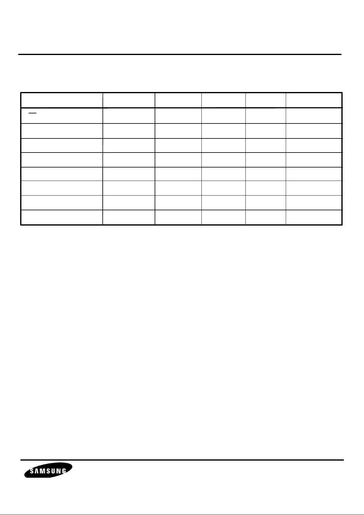
ABSOLUTE MAXIMUM RATINGS ( Ta = 25 °C )
Characteristic
Positive Digital Supply Voltage
Positive Analog Supply Voltage
Negative Analog Supply Voltage
Power Dissipation
Operating Temperature
Storage Temperature
Symbol
V
DD
V
CC
V
BB
P
D
T
OPR
T
STG
- 9 -
Value
5V ± 5%
5V ± 5%
-5V ± 5%
400 (KS16112) 550 (KS16114)
0 ~ 70
-55 ~ 150
Unit
V
V
V
mW
°C
°C

KS16112/4
9600/14400 bps FAX MODEM
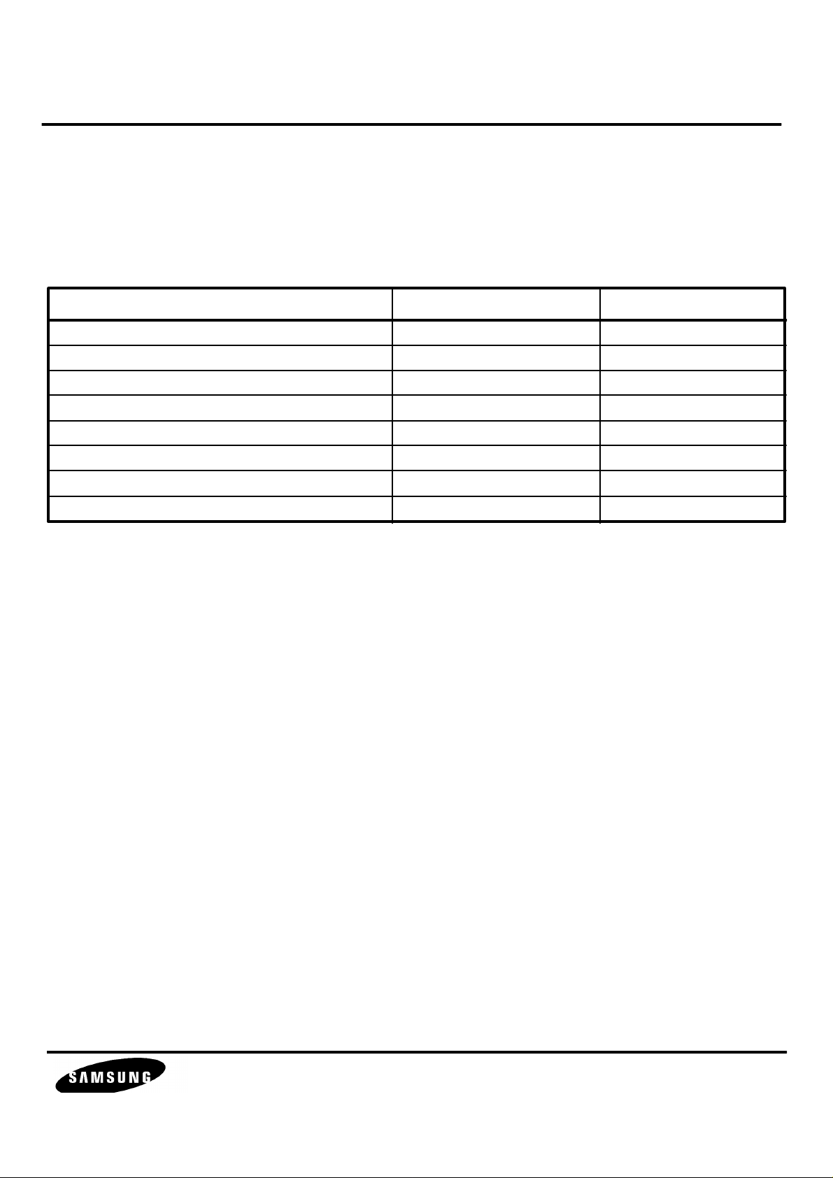
ELECTRICAL CHARACTERISTICS
( Ta = 25 °C , VCC = 5V, VBB = -5V, Unless otherwise specified )
Characteristic
Input Voltage
Input Current
Input Leakage
Current
Output Leakage
Current
Output Voltage
V.24 Signals,
TTL
PORI
TTL
TTL w / p - up
PORITTL and
TTL 3 - S
TTL 3 - S
PORO
Symbol
V
IH
V
IL
I
IH
I
IL
I
I( LKG )
I
O( LKG )
V
OH
Test Condition
VCC = 5.25V, Vin = 5.25V
VCC = 5.25V
VCC = 5.25V
Vin = 0 to 5V
Vin = 0.4 to V
I
= -100 µA
LOAD
I
= -40 µA
LOAD
CC
- 1
Min
2.0
0.8V
-0.3
3.5
2.4
Typ Max Unit
V
CC
V
0.8
40
-400
± 2.5
± 10
CC
CC
V
V
µA
µA
µA
µA
V
V.24 Signals,
Clock Output
Current
Capacitive Load
Capacitive Drive
IRQ
D0 - D7
PORO
TTL and
PORI
TTL w / p - up
TTL 3-S and Open
Drain CLOCK
V
OL
I
OH( CLK )
I
OL( CLK )
C
L
C
D
I
LOAD
I
LOAD
I
LOAD
= 1.6mA
= 0.8mA
= 0.4mA
5
20
100
50
0.4
0.4
0.4
-0.1
100
V
mA
µA
PF
PF
- 10 -
KS16112/4
9600/14400 bps FAX MODEM
MICROPROCESSOR INTERFACE TIMING CHARACTERISTICS ( Ta = 25 °C )
Characteristics Symbol Min Typ Max Unit
CS Set up time
RSI Set up time
Data access time
Data hold time
Control hold time
Write data set up time
Write data hold time
Phase 2 Clock high
t
CS
t
RS
t
DA
t
DHR
t
HC
t
WDS
t
DHW
t
2CH
0
25
10
10
20
10
100
75
nSec
nSec
nSec
nSec
nSec
nSec
nSec
nSec
- 11 -

KS16112/4
9600/14400 bps FAX MODEM
CS
t
RS
RS0 - RS4
WRITE
READ
D0 - D7
CS
t
RS
READ WRITE
t
WDS
t
CS
t
HC
t
DHW
t
CS
t
DA
t
HC
t
DHR
t
RS
a. 8085 Bus Compatible ( EN85 = “L” )
READ WRITE
t
CS
t
HC
t
RS
t
CS
t
HC
RS0 - RS4
R / W
Ø2
D0 - D7
t
2CH
t
DA
t
DHR
t
WDS
t
DHW
b. 6500 Bus Compatible ( EN85 = “H” )
Figure 1. MICROPROCESSOR BUS INTERFACE TIMING DIAGRAM
- 12 -

KS16112/4
9600/14400 bps FAX MODEM
TECHNICAL SPECIFICATIONS
1 Configurations, Signaling Rates and Data Rates
The various modem configurations with the corresponding modulation specifications are shown in Table 7.
Table 7. Modulation Specifications
Configuration
V.17 14400
( KS16114 )
V.17 12000
( KS16114 )
V.17 9600
( KS16114 )
V.17 7200
( KS 16114 )
V.29 9600
V.29 7200
V.29 4800
Modulation
Scheme
TCM
TCM
TCM
TCM
QAM
QAM
QAM
Carrier Fre quency ( Hz )
1800
1800
1800
1800
1700
1700
1700
Data Rate
( bps )
14400
12000
9600
7200
9600
7200
4800
Data Rate
( Symbols/Sec. )
2400
2400
2400
2400
2400
2400
2400
No of Bits
per Symbol
6
5
4
3
4
3
2
No. of Signal
Points
128
64
32
16
16
8
4
V.27 ter 4800
V.27 ter 2400
V.21 Ch2 300
2 Transmitted Data Spectrum
The transmitted data spectrum is shaped with the following characteristics:
At 2400 baud a square root of 25% raised cosine filter is used.
At 1600 baud a square root of 50% raised cosine filter is used.
At 1200 baud a square root of 90% raised cosine filter is used.
DPSK
DPSK
FSK
1800
1800
1650, 1850
4800
2400
300
- 13 -
1600
1200
300
3
2
1
8
4
KS16112/4
3 Turn - On Sequence
The transmitter turn - on sequence times are shown in Table 8.
Table 8. Turn - On Sequence Duration
9600/14400 bps FAX MODEM
Configuration
V.17 long train ( all speeds ) ( KS16114 )
V.17 short train ( all speeds ) ( KS16114 )
V.29 ( all speeds )
V.27 ter 4800 bps long train
V.27 ter 4800 bps short train
V.27 ter 2400 bps long train
V.27 ter 2400 bps short train
V.21 Ch2 300 bps
4 Turn - Off Sequence
The turn - off sequence consists of:
- for V.17 ( KS16114 ) approximately 14 ms of remaining data and scrambled ones
followed by 20 ms of silence.
- for V.29 approximately 5 ms of remaining data and scrambled ones followed by 20
ms of silence
- for V.27 ter approximately 10 ms of remaining data and scrambles ones ( 1200 baud )
and 7 ms of data and scrambled ones ( 1600 baud ) and 20 ms of silence.
- for V.21 ch 2 the transmitter turns-off within 7 ms after RTS goes inactive.
EPTE OFF
1393 ms
142 ms
253 ms
708 ms
50 ms
943 ms
67 ms
< 400 us
EPTE ON
1600 ms
350 ms
441 ms
915 ms
257 ms
1150 ms
274 ms
< 400 us
5 Data Encoding
The data encoding is in accordance with ITU-T recommendations V.17 ( KS16114 ), V.29, V.27 ter, V.21
Channel 2, and T.3.
6 Equalization
Required line equalization is implemented in V.17 ( KS16114 ), V.29 and V.27 ter modes with an adaptive
48 - tap T/2 transversal equalizer.
- 14 -

KS16112/4
7 Tone Generation
The modem is capable of generating single or dual tones in the frequency range of 400 to 3200 Hz with a
resolution of 0.15 Hz and accuracy of 0.01%. This feature allows the modem to function as a DTMF dialer.
8 Transmit Level
The transmitter output level is programmable from 0 dBm to - 15.0 dBm and is accurate to ± 1.0 dB.
9 Scrambler / Descrambler
The scrambler and descrambler are in accordance with ITU-T recommendations V.17 ( KS16114 ), V.29 and
V.27ter.
10 Receiver Dynamic Range
The receiver can operate with line signal levels from 0 dBm to - 43 dBm at the receiver analog input
( RXAI ). The RLSD threshold levels are programmable as follows:
9600/14400 bps FAX MODEM
Turn on: - 10 dBm to - 47 dBm ( default = - 43 dBm )
Turn off: - 10 dBm to - 52 dBm ( default = - 48 dBm )
11 Receiver Timing
The receiver can track a timing error of up to ± 0.035%
12 Carrier Recovery
The receiver can track a frequency offset up to ± 10 Hz.
13 Received Data
The serial received data output ( RXDO ) is clamped to a constant mark whenever RLSD is off.
14 Tone Detection
The modem features three tone detectors two of which operate in all non - high speed modes. The third
tone detector operates in all receive modes. The three tone detectors can be cascaded to form a single
12th order filter. The filter coefficients of each tone detector are programmable by the host.
- 15 -

KS16112/4
15 Power Requirements
The power requirements are as follows:
+ 5V ± 5% @ 60 mA ( typical : KS16112 ), @95mA ( typical : KS16114 )
- 5V ± 5% @ 14 mA ( typical )
16 Environmental Requirements
The environmental requirements are as follows:
Temperature operating range from 0 - 70 °C.
17 Differences Between the Samsung KS16112/4 and Rockwell R96DFX/R144EFX
The KS16112/4 are pin - to- pin and software compatible modem devices that can be used to replace
the Rockwell R96DFX /R144EFX modem. Functionally, the Samsung and Rockwell modems are nearly
identical. However, there are a few differences between the two that the user should be aware of.
9600/14400 bps FAX MODEM
• The KS16112/4 feature an improved equalizer with 48 taps thus allowing better performance without a
compromise equalizer. The KS16112/4 work over 7 Japanese links as well as over all EIA lines.
The equalizer is always T/2 fractionally spaced and there is no provision for a T-spaced equalizer.
Also when reading the equalizer taps from the DSP it should be noted that the direction of the time axis
is different from Rockwell’s ( i.e the smallest address corresponds to the oldest data ). The tap coefficients
between the Samsung KS16112/4 and Rockwell R96DFX / R144EFX are not interchangeable ( i.e taps
stored from the R96DFX / R144EFX cannot be loaded into the KS16112/4 ).
• Instantaneous energy detector ( IED ) does not include state 2.
• During DTMF detection the DEDT bit is the same as the DTDT bit.
• The following DTMF parameters are not available:
Minimum cycle time
Minimum dropout time ( is always set to 5 ms )
Frequency deviation, low group
Frequency deviation, high group
Maximum energy hit time
• Programmable Interrupt does not include dual port interface memory locations 0 and 10.
- 16 -

KS16112/4
Maximum speed energy ( CR1=1 , ADDR1=1E ) works differently from Rockwell. Maximum speech energy sets
• The signal level should be derived from the AGC gain word since the average energy is not implemented.
• The carrier detect turn - on and carrier detect turn - off thresholds function differently from the R96DFX /
R144EFX .
The carrier thresholds should be changed by changing MAXG ( MAXG is R96DFX /R144EFX compatible ).
• Samsung modem does not support squelch extend.
• The host should complete high speed configuration change prior to 30mS before receiving data.
• The host should not write data into DBFR during RTS to CTS in HDLC mode
•
the ratio between the total energy and the DTMF tone energy before valid DTMF digits are detected.
The default is 4000 hex which is 3dB.
9600/14400 bps FAX MODEM
• 1800pF capacitor must be connected between AGCIN and GNDA1 OR GNDA2.
• Data speed detection of V.33 is not supported ( KS16114 ).
• 1700 HZ carrier for V.17 is not supported ( KS16114 ).
• Samsung modem provides a host programmable receiver compromise filter.
• G2 mode is not supported ( KS16114 ).
• Voice mode is not supported ( KS16114 ).
• IRQ2 is not supported ( KS16114 ).
- 17 -

KS16112/4
• DSP memory bits that are not supported
KS16112 does not support Rockwell R96DFX DSP memory
• 07:2 SQEXT
• 07:1 T2
KS16114 does not support R144EFX DSP memory
• 1E:4 B2I2E
• 1E:1 B1I2E
• 1D:7 SHPR
• 1D:6 ASPEED
• 1D:5 PR
• 1D:4 PRDET
• 15:6 AREX2
• 15:4 DR2
• 0E:7 FSKFLS
• 0D:3 G2FGC
• 08:2 FSK7E
• 08:1 G2CTK
• 07:2 SQEXT
• 05:6 AREX1
• 05:5 PIDR
• 05:4 DR1
9600/14400 bps FAX MODEM
- 18 -

KS16112/4
or coefficient RAM if CRAM1=1) during a RAM access cycle. The 16-bit real and imaginary data to be written
9600/14400 bps FAX MODEM
SOFTWARE INTERFACE
Communication between the modem and the host microprocessor is accomplished by means of a dual port
interface memory. The dual port memory consists of 32 8-bit registers that both the host microprocessor
and the modem have access to. The host can control modem operation by writing control bits or
parameter values to the dual port interface memory. The host can also monitor modem operation by reading
status bits or data values ( such as the eye quality monitor value or EQM ) from the interface memory.
The dual port read and write procedures are described in section 3.
1. Dual - Port Memory Map
The memory map for the 32 - byte interface memory registers is shown in Table 1. These registers can be
accessed during any host read or write cycle. In order to operate on a single bit or a group of bits, the
host microprocessor must first read the desired register, set or reset the desired bits and then write the
modified and unmodified bits back into the interface memory register.
2 Modem Interface Memory Bit Definitions
This section describes in detail the function of all bits, fields and registers in the interface memory. All bit,
field or register names are listed in alphanumeric order. For each bit, field or register the convention
R :B ( D ) is used to indicate the location of the term and its power up default value. R is the register
number ( hexadecimal ), B is the bit or group of bits within that register and D is the associated power up
default value. A default value of ‘- ’ indicates that the bit state depends on modem operating conditions,
thus, these bits do not truly have a power up default value.
ABORT 09 : 3 ( - )Abort/Idle
In the transmit mode when ABORT is set the modem will finish sending the current DBFR byte after which
it will send continuous ones ( if ZCLMP is reset ) or continuous zeros ( if ZCLMP is set ). When ABORT
is reset the modem will not send continuous ones or zeros.
In the receive mode when ABORT is set the modem has received a minimum of seven consecutive ones.
ABORT must then be reset by the host.
Address 1ADR 1
ADR1 is used to specify the modem’s internal RAM address to be read or written ( data RAM if CRAM1=0
04 : 0 - 7 ( 17h )
into RAM or read out of RAM is placed in XDM1, XDL1 and YDM1, YDL1. The address value in ADR1 also
determines the data to be output by the modem via the eye pattern interface ( SEPXO and SEPYO ). At
power-up, ADR1 defaults to 17h which corresponds to the rotated equalizer output ( normal eye pattern
output ).
- 19 -

KS16112/4
internal RAM address to be read or written ( data RAM if CRAM2 = 0
ADR2 Address2 14 : 0 - 7 ( - )
ADR2 is used to specify the modem’s
or coefficient RAM if CRAM2 = 1 ) during a RAM access cycle. The 16 - bit real and imaginary data to be
written into RAM or read out of RAM is placed in XDM2, XDL2 and YDM2, YDL2.
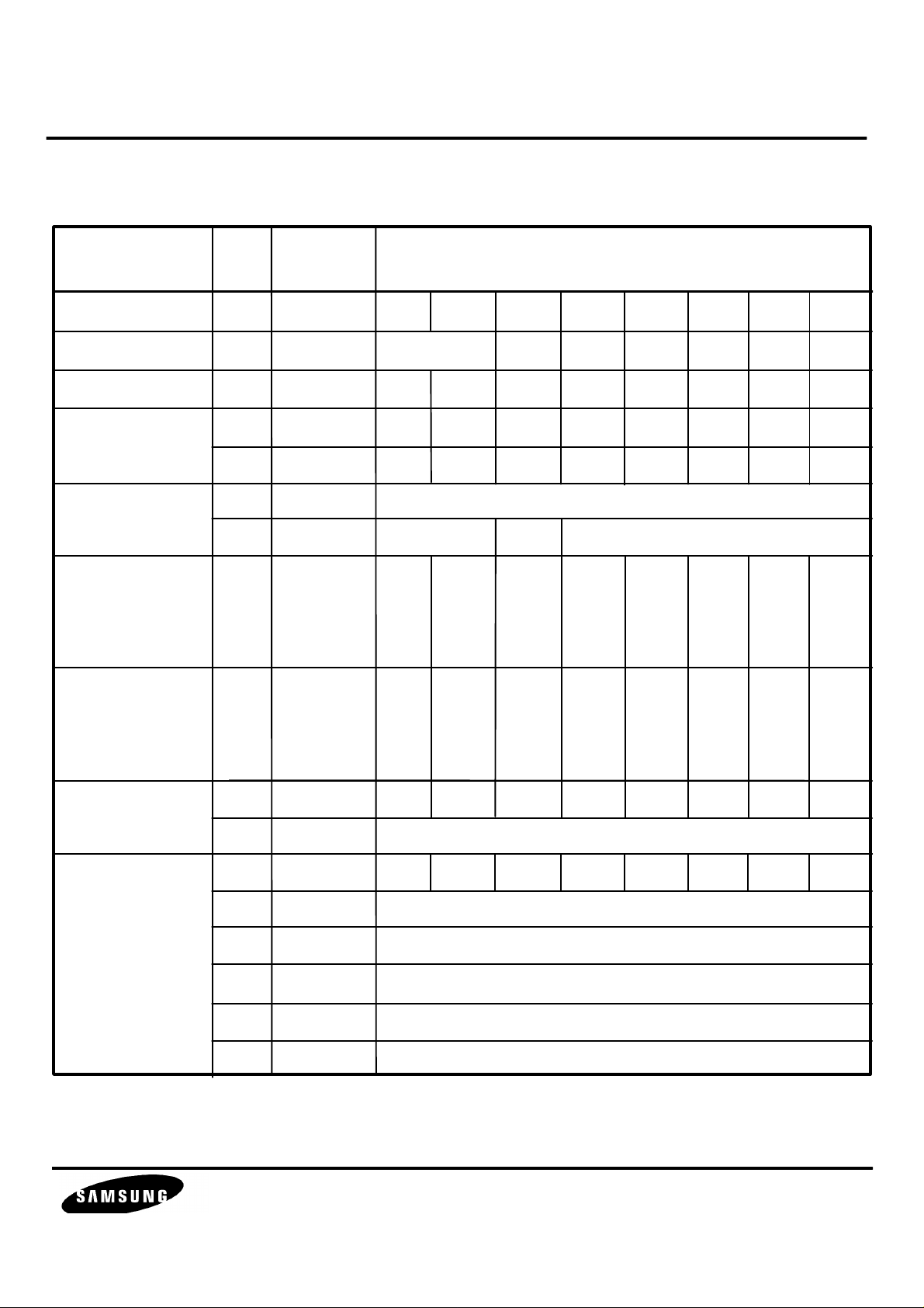
Table 1. Dual Port Interface Memory Map
9600/14400 bps FAX MODEM
Register Function
Interrupt Handling
Not Used
DTMF Status
Not Used
Reg.
Addr.
( Hex )
1F
1E
1D
1C
1B
1A
19
18
17
16
Default
Value ( Bin )
- XX0 - XX0
- - 0X - 0X XXXXXXXX
- - - - - - - XXXXXXXX
XXXXXXXX
XXXXXXXX
XXXXXXXX
XXXXXXXX
XXXXXXXX
7
PINTA
INTA2
DEDT
-
-
-
-
-
-
6
INTA1
DTDT
-
-
-
-
-
-
5
INTE2
DOTS
-
-
-
-
-
-
4
PINTE
-
DSDET
-
-
-
-
-
-
Bit
3
PIRQ
BDA2
-
-
-
-
-
-
-
2
INTE1
DTMFW
-
-
-
-
-
-
1
-
-
-
-
-
-
-
-
-
0
CSET
BDA1
-
-
-
-
-
-
-
15
RAM Access2
Control and Status
and Parallel Data
Buffer
14
13
12
11
10
00000000
- - - - - - - -
- - - - - - - -
- - - - - - - -
- - - - - - - -
- - - - - - - -
RA2
RAM ADDRESS2 ( ADR2 )
X RAM DATA2 MSB ( XDM2 )
X RAM DATA2 LSB ( XDL2 )
Y RAM DATA2 MSB ( YDM2 )
Y RAM DATA2 LSB ( YDL2 ) / DATA BUFFER ( DBFR )
- 20 -
AHEOF
-
-
BRT2
WT2
CRAM2
KS16112/4
Table 1. Dual Port Interface Memory Map ( Continued )
9600/14400 bps FAX MODEM
Register Function
Modem Status
Not Used
High Speed Status
Programmable
Interrupt Control
High Speed Control
and HDLC Control
and Status
Tone Detect and
Reg.
Addr.
( Hex )
0F
0E
0D
0C
0B
0A
09
Default
Value ( Bin )
- - XXXX - XXXXXXXX
- - XXXXXX
XX - - - - - 00000000
00000000
- 000 - - - -
7
IED
REC
-
ITRG
ORUR
6
PNDT
-
SAVEQ
5
-
-
DATM
INTML
FRZEQ
4
-
-
SCR1S
INTMSK
ZCLMP
Bit
3
-
-
PNS
ABORT
2
-
-
P2S
INTADR
EOHF
1
CTSB
-
P1S
CRCE
0
DCDB
-
SILIDL
FLG
High Speed Control
& Status
Mode Control
RAM Access1
Control & Status
and Programmable
Interrupt Control
08
07
06
05
04
03
02
01
00
- - - 0 - XXX
00001000
00010100
10000101
00010111
- - - - - - - -
- - - - - - - -
- - - - - - - -
- - - - - - - -
TD3
RTSB
RA1
TD2
TRND
-
TD1
PDME
RAM ADDRESS1 ( ADR1 )
X RAM DATA1 MSB ( XDM1 )
X RAM DATA1 LSB ( XDL1 )
Y RAM DATA1 MSB ( YDM1 )
Y RAM DATA1 LSB ( YDL1 )
CASC
SHTRN
-
PNSX
EPTE
CONFIG
-
-
-
BRT1
-
-
WT1
-
HDLCE
CRAM1
- 21 -
 Loading...