

Samsung KS0718 Datasheet
KS0718
written permission of LCD Driver IC Team.
81 COM / 104 SEG DRIVER & CONTROLLER FOR STN LCD
Contents in this document are subject to change without notice. No part of this document may be reproduced
or transmitted in any form or by any means, electronic or mechanical, for any purpose, without the express
August. 1999.
Ver. 1.4
Prepared by: Chan-Young, Jeong
Cyjeong7@samsung.co.kr
81 COM / 104 SEG DRIVER & CONTROLLER FOR STN LCD SPEC. VER. 1.4 KS0718
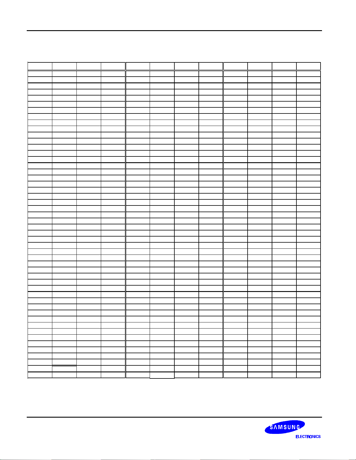
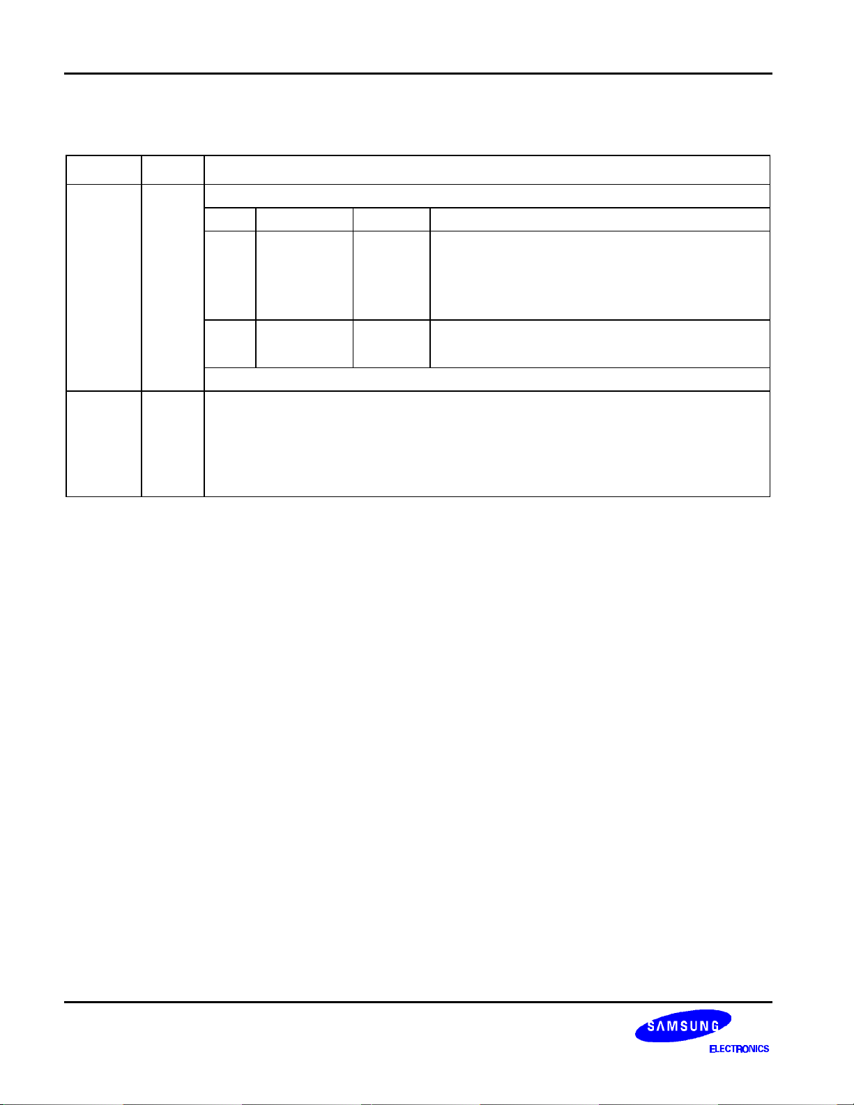
KS0718 Specification Revision History
Version Content Date
0.0 Original Nov.1998
Modify syntax errors
0.1
Append n-line inversion wave form to figure 11 on page 19.
Dec.1998
Modify figure 12 on page 20
Change the number of COM/SEG (85COM / 100SEG -> 81COM /
1.0
104SEG)
Mar.1999
Modify PAD location
1.1
Append PAD center coordinates to table 1, 2 on page 4, 5
Append referential instruction setup flow on page 48 to 51
Apr.1999
Change bumped PAD size (modify figure 2 and table 1 on page 3)
Change the PAD Center Coordinates of COM39 and COMS1.
1.2
(modify table 2 on page 4)
May.1999
Change LCD power supply voltage
(modify VOUT and V0 voltage on page1, 52, 53, 54, 55)
Modify Set partial display duty ratio (refer to page 32)
Modify N-line Inversion Register “2 to 32” -> “3 to 33” (refer to page 41)
1.3
Change Consumption Current “2mA” -> “2uA”, “10mA” -> “10uA”
(refer to page 47)
Jun.1999
Add Partial Duty Changing “Waiting for Discharging the LCD Power
Levels (refer to figure 39)
1.4
Fix the TBD Value of DC/AC Characteristics.
Aug.1999
2
KS0718 SPEC. VER. 1.4 81 COM / 104 SEG DRIVER & CONTROLLER FOR STN LCD
CO
NTENTS
INTRODUCTION ..................................................................................................................................................1
BLOCK DIAGRAM...............................................................................................................................................2
PAD CONFIGURATION .......................................................................................................................................3
PAD CENTER COORDINATES ............................................................................................................................5
PIN DESCRIPTION ..............................................................................................................................................7
POWER SUPPLY ..........................................................................................................................................7
LCD DRIVER SUPPLY..................................................................................................................................7
SYSTEM CONTROL .....................................................................................................................................8
MICROPROCESSOR INTERFACE...............................................................................................................9
LCD DRIVER OUTPUTS.............................................................................................................................11
FUNCTIONAL DESCRIPTION............................................................................................................................ 12
MICROPROCESSOR INTERFACE.............................................................................................................12
DISPLAY DATA RAM (DDRAM)..................................................................................................................15
LCD DISPLAY CIRCUITS............................................................................................................................19
LCD DRIVER CIRCUIT ...............................................................................................................................21
POWER SUPPLY CIRCUITS ......................................................................................................................24
REFERECE CIRCUIT EXAMPLES..............................................................................................................29
RESET CIRCUIT.........................................................................................................................................31
INSTRUCTION DESCRIPTION...........................................................................................................................32
SPECIFICATIONS..............................................................................................................................................52
ABSOLUTE MAXIMUM RATINGS...............................................................................................................52
DC CHARACTERISTICS .............................................................................................................................53
AC CHARACTERISTICS.............................................................................................................................56
REFERENCE APPLICATIONS........................................................................................................................... 61
MICROPROCESSOR INTERFACE.............................................................................................................61
CONNECTIONS BETWEEN KS0718 AND LCD PANEL..............................................................................62
3
KS0718 SPEC. VER. 1.4 81 COM / 104 SEG DRIVER & CONTROLLER FOR STN LCD
INTRODUCTION
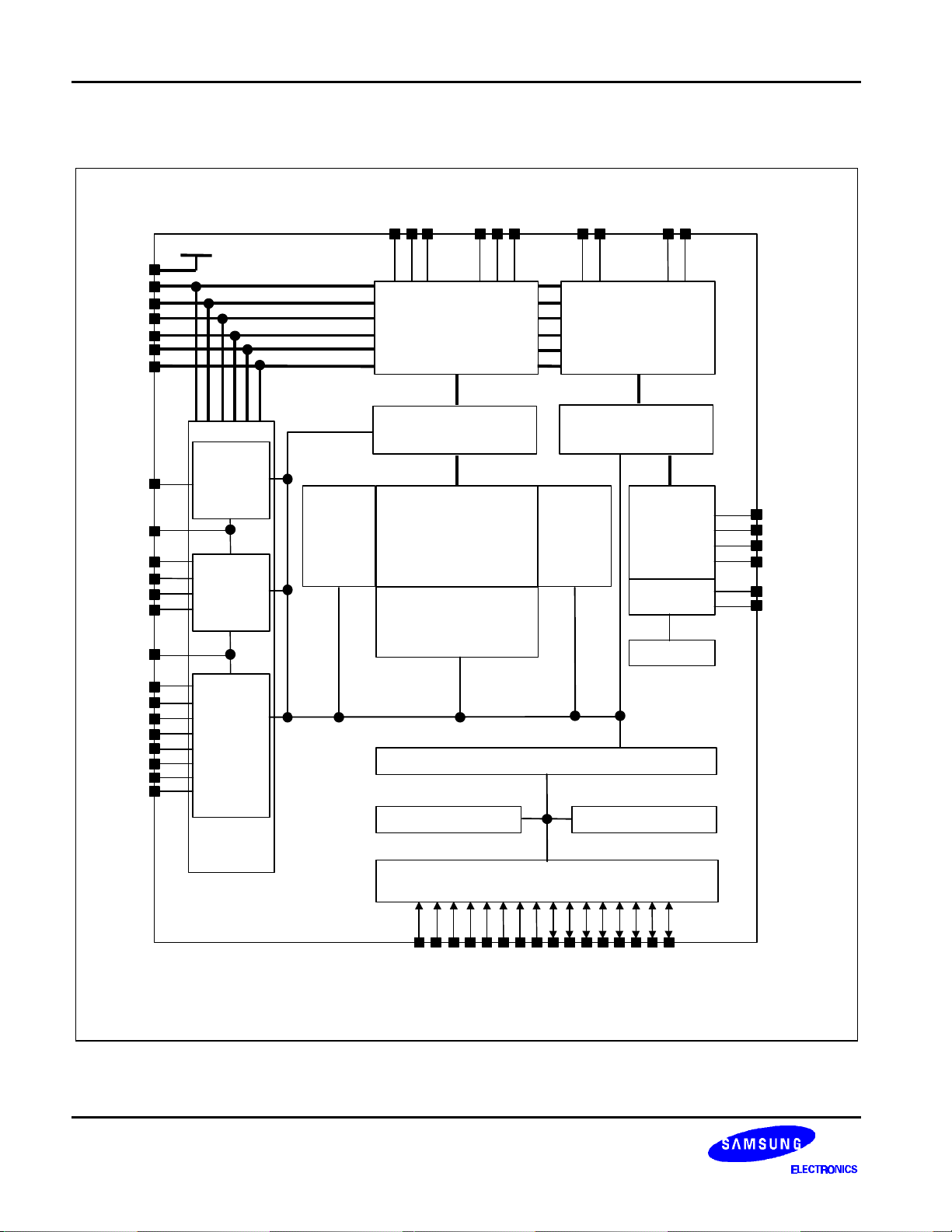
The KS0718 is a driver & controller LSI for graphic dot-matrix liquid crystal display systems. It contains 81
common and 104 segment driver circuits. This chip is connected directly to a microprocessor, accepts serial or 8bit parallel display data and stores in an on-chip display data RAM of 89 x 104 bits. It provides a highly flexible
display section due to 1-to-1 correspondence between on-chip display data RAM bits and LCD panel pixels. And it
performs display data RAM read/write operation with no externally operating clock to minimize power
consumption. In addition, because it contains power supply circuits necessary to drive liquid crystal, it is possible
to make a display system with the fewest components.
FEATURES
Driver Output Circuits
− 81 common outputs / 104 segment outputs
Applicable Duty Ratios
Programmable duty ratio Applicable LCD bias Maximum display area
1/9 to 1/81 1/4 to 1/11
− Various partial display
− Partial window moving & data scrolling
On-chip Display Data RAM
81 × 104
− Capacity: 89 x 104 = 9,256 bits
− Bit data "1": a dot of display is illuminated.
− Bit data "0": a dot of display is not illuminated.
Microprocessor Interface
− 8-bit parallel bi-directional interface with 6800-series or 8080-series
− Serial interface (only write operation) available
On-chip Low Power Analog Circuit
− On-chip oscillator circuit
− Voltage converter (x3, x4, x5 or x6)
− Voltage regulator (temperature coefficient: -0.05%/°C or external input)
− On-chip electronic contrast control function (64 steps)
− Voltage follower (LCD bias: 1/4 to 1/11)
Operating Voltage Range
− Supply voltage (VDD): 2.4 to 5.5 V
− LCD driving voltage (VLCD = V0 - VSS): 4.0 to 15.0 V
Low power Consumption
− 150 µΑ Max. (VDD = 3V, x5 boosting, V0 = 12V, internal power supply on and display OFF)
− 15 µΑ Max. (during power save [standby] mode)
Package Type
− Gold bumped chip or TCP
1
81 COM / 104 SEG DRIVER & CONTROLLER FOR STN LCD SPEC. VER. 1.4 KS0718
DB0
DB1
COMS1
COM
BLOCK DIAGRAM
SEG103
SEG102
VDD
V0
V1
V2
V3
V4
VSS
:
SEG101
:
SEG2
SEG1
SEG0
104 SEGMENT
DRIVER CIRCUITS
COMS
COM0
:
:
:
82 COMMON
DRIVER CIRCUITS
79
HPMB
V0
VR
INTRS
VEXT
REF
VOUT
C1-
C1+
C2C2+
C3+
C4+
C5+
VCI
V / F
CIRCUIT
V / R
CIRCUIT
V / C
CIRCUIT
INTERNAL
POWER
SUPPLY
PAGE
ADDRESS
CIRCUIT
SEGMENT CONTROLLER
DISPLAY DATA RAM
89 X 104 = 9,256 Bits
COLUMN ADDRESS
CIRCUIT
INSTRUCTION DECODER & REGISTER
MPU INTERFACE (PARALLEL & SERIAL)
COMMON CONTROLLER
DISPLAY
LINE
ADDRESS
CIRCUIT
STATUS REGISTERBUS HOLDER
TIMING
GENERATOR
CIRCUIT
STATIC
DRIVER
OSCILLATOR
MS
CL
SYNC
M
FRS
FR
DB2
DB3
DB4
DB5
DB6(SCLK)
DB7(SID)
RW_WR
E_RD
RS
CS2
CS1B
PS
C68
RESETB
Figure 1. Block Diagram
2
KS0718 SPEC. VER. 1.4 81 COM / 104 SEG DRIVER & CONTROLLER FOR STN LCD
Y
(0,0)
X
ðððð
- - - -
ððð
ð
ðððð
- - - -
ððð
ð
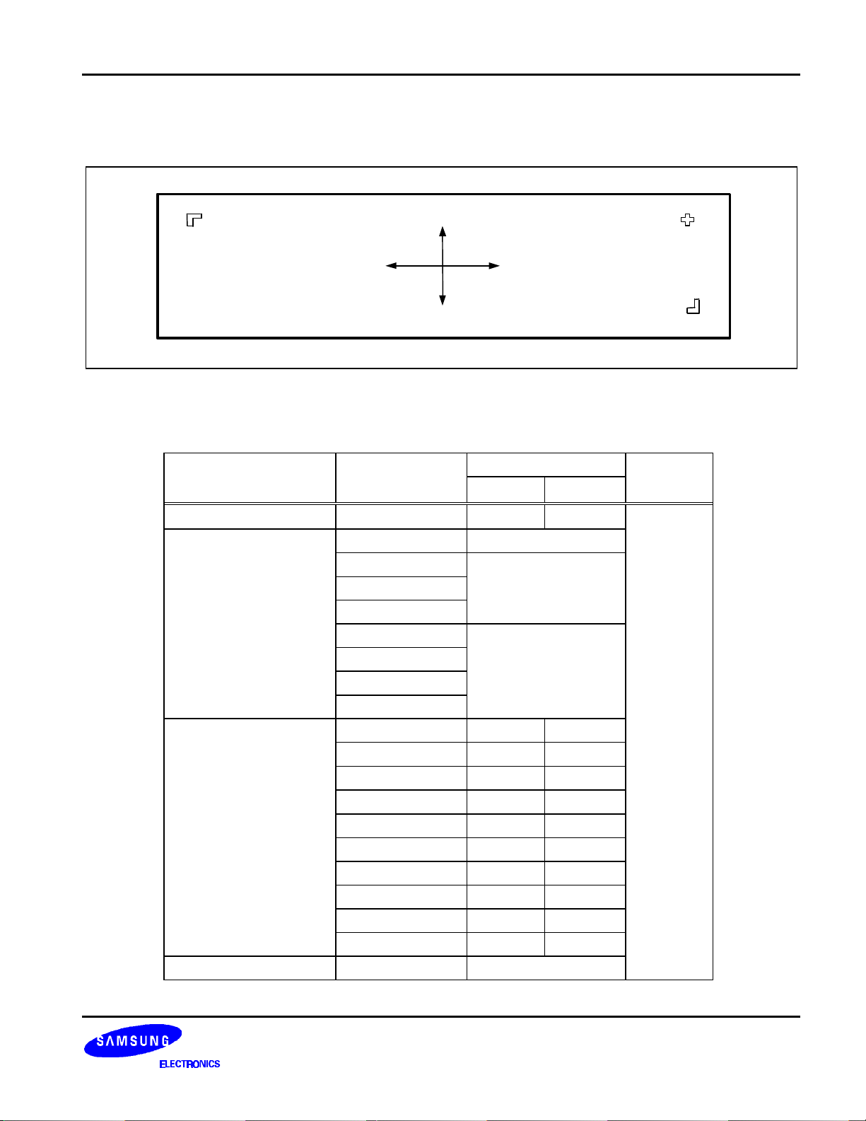
PAD CONFIGURATION
113242
243
рр ррррррррррррррррррр
KS0718
(TOP VIEW, PADS UP)
- - - - - - - - - -
ррррррррррррррррррр
ðð
112
274
рррррррррррррррррррррр
1
Figure 2. KS0718 Chip Configuration
Table 1. KS0718 Pad Dimensions
Item Pad No.
Chip size - 8350 2380
Pad pitch
- - - - - - - - - -
1 to 80 90
82 to 110
115 to 240
245 to 273
81
111 to 114
241 to 244
274
1 to 80 54 112
81 110 80
ррррррррррррррррррррррр
X Y
81
80
Size
Unit
60
80
µm
82 to 110 110 40
111 to 112 110 60
Bumped pad size (Max.)
Bumped pad height All pad 14 (Typ.)
113 to 114 60 110
115 to 240 40 110
241 to 242 60 110
243 to 244 110 60
245 to 273 110 40
274 110 80
3
81 COM / 104 SEG DRIVER & CONTROLLER FOR STN LCD SPEC. VER. 1.4 KS0718
30µm
30µm
30µm
42µm
108µm
42µm
108µm
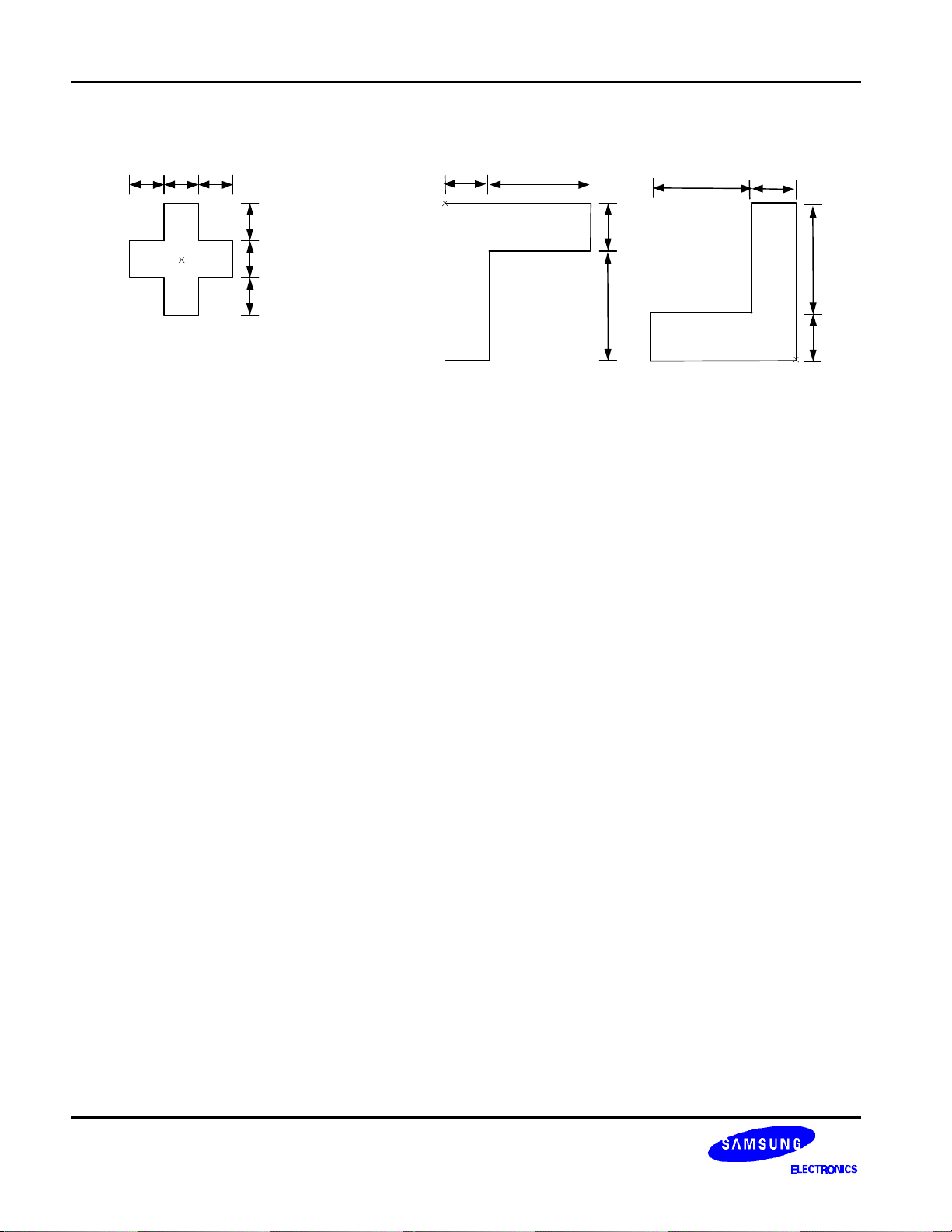
COG Align Key Coordinate ILB Align Key Coordinate
30µm 30µm 30µm
(+3565, +640)
42µm 108µm
(-3493.5, -488.5)
42µm108µm
(+3493.5, +408.5)
4
KS0718 SPEC. VER. 1.4 81 COM / 104 SEG DRIVER & CONTROLLER FOR STN LCD
50
C5+
855
-1066
100
COM20
4028
130
150
SEG24
1650
1043
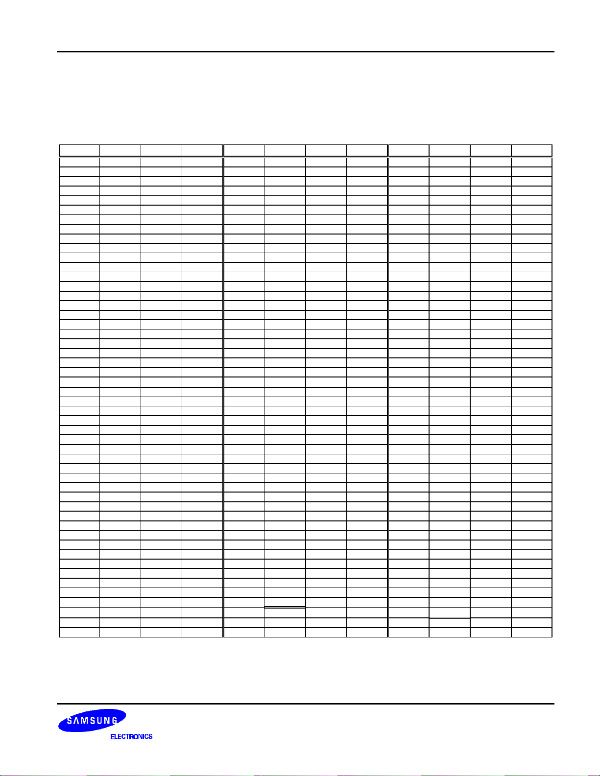
PAD CENTER COORDINATES
Table 2. Pad Center Coordinates
[Unit: µm]
No. Name X Y No. Name X Y No. Name X Y
1 FRS -3555 -1066 51 C3+ 945 -1066 101 COM19 4028 190
2 FR -3465 -1066 52 C3+ 1035 -1066 102 COM18 4028 250
3 TEST1 -3375 -1066 53 C1- 1125 -1066 103 COM17 4028 310
4 TEST2 -3285 -1066 54 C1- 1215 -1066 104 COM16 4028 370
5 TEST3 -3195 -1066 55 C1+ 1305 -1066 105 COM15 4028 430
6 CL -3105 -1066 56 C1+ 1395 -1066 106 COM14 4028 490
7 M -3015 -1066 57 C2+ 1485 -1066 107 COM13 4028 550
8 SYNC -2925 -1066 58 C2+ 1575 -1066 108 COM12 4028 610
9 VSS -2835 -1066 59 C2- 1665 -1066 109 COM11 4028 670
10 HPMB -2745 -1066 60 C2- 1755 -1066 110 COM10 4028 730
11 MS -2655 -1066 61 C4+ 1845 -1066 111 DUMMY 4028 810
12 VDD -2565 -1066 62 C4+ 1935 -1066 112 DUMMY 4028 890
13 PS -2475 -1066 63 VSS 2025 -1066 113 DUMMY 3910 1043
14 C68 -2385 -1066 64 REF 2115 -1066 114 DUMMY 3830 1043
15 VSS -2295 -1066 65 VEXT 2205 -1066 115 COM9 3750 1043
16 CS1B -2205 -1066 66 VDD 2295 -1066 116 COM8 3690 1043
17 CS2 -2115 -1066 67 INTRS 2385 -1066 117 COM7 3630 1043
18 VDD -2025 -1066 68 VSS 2475 -1066 118 COM6 3570 1043
19 RESETB -1935 -1066 69 V4 2565 -1066 119 COM5 3510 1043
20 RS -1845 -1066 70 V4 2655 -1066 120 COM4 3450 1043
21 VSS -1755 -1066 71 V3 2745 -1066 121 COM3 3390 1043
22 RW_WR -1665 -1066 72 V3 2835 -1066 122 COM2 3330 1043
23 E_RD -1575 -1066 73 V2 2925 -1066 123 COM1 3270 1043
24 VDD -1485 -1066 74 V2 3015 -1066 124 COM0 3210 1043
25 DB0 -1395 -1066 75 V1 3105 -1066 125 COMS 3150 1043
26 DB1 -1305 -1066 76 V1 3195 -1066 126 SEG0 3090 1043
27 DB2 -1215 -1066 77 V0 3285 -1066 127 SEG1 3030 1043
28 DB3 -1125 -1066 78 V0 3375 -1066 128 SEG2 2970 1043
29 DB4 -1035 -1066 79 VR 3465 -1066 129 SEG3 2910 1043
30 DB5 -945 -1066 80 VR 3555 -1066 130 SEG4 2850 1043
31 DB6 -855 -1066 81 COM39 4028 -1030 131 SEG5 2790 1043
32 DB7 -765 -1066 82 COM38 4028 -950 132 SEG6 2730 1043
33 VDD -675 -1066 83 COM37 4028 -890 133 SEG7 2670 1043
34 VDD -585 -1066 84 COM36 4028 -830 134 SEG8 2610 1043
35 VDD -495 -1066 85 COM35 4028 -770 135 SEG9 2550 1043
36 VDD -405 -1066 86 COM34 4028 -710 136 SEG10 2490 1043
37 VDD -315 -1066 87 COM33 4028 -650 137 SEG11 2430 1043
38 VCI -225 -1066 88 COM32 4028 -590 138 SEG12 2370 1043
39 VCI -135 -1066 89 COM31 4028 -530 139 SEG13 2310 1043
40 VSS -45 -1066 90 COM30 4028 -470 140 SEG14 2250 1043
41 VSS 45 -1066 91 COM29 4028 -410 141 SEG15 2190 1043
42 VSS 135 -1066 92 COM28 4028 -350 142 SEG16 2130 1043
43 VSS 225 -1066 93 COM27 4028 -290 143 SEG17 2070 1043
44 VSS 315 -1066 94 COM26 4028 -230 144 SEG18 2010 1043
45 VOUT 405 -1066 95 COM25 4028 -170 145 SEG19 1950 1043
46 VOUT 495 -1066 96 COM24 4028 -110 146 SEG20 1890 1043
47 VOUT 585 -1066 97 COM23 4028 -50 147 SEG21 1830 1043
48 VOUT 675 -1066 98 COM22 4028 10 148 SEG22 1770 1043
49 C5+ 765 -1066 99 COM21 4028 70 149 SEG23 1710 1043
5
81 COM / 104 SEG DRIVER & CONTROLLER FOR STN LCD SPEC. VER. 1.4 KS0718
200
SEG74
-1350
1043
250
COM56
-4028
430
Table 2. Pad Center Coordinates (Continued)
[Unit: µm]
No. Name X Y No. Name X Y No. Name X Y
151 SEG25 1590 1043 201 SEG75 -1410 1043 251 COM57 -4028 370
152 SEG26 1530 1043 202 SEG76 -1470 1043 252 COM58 -4028 310
153 SEG27 1470 1043 203 SEG77 -1530 1043 253 COM59 -4028 250
154 SEG28 1410 1043 204 SEG78 -1590 1043 254 COM60 -4028 190
155 SEG29 1350 1043 205 SEG79 -1650 1043 255 COM61 -4028 130
156 SEG30 1290 1043 206 SEG80 -1710 1043 256 COM62 -4028 70
157 SEG31 1230 1043 207 SEG81 -1770 1043 257 COM63 -4028 10
158 SEG32 1170 1043 208 SEG82 -1830 1043 258 COM64 -4028 -50
159 SEG33 1110 1043 209 SEG83 -1890 1043 259 COM65 -4028 -110
160 SEG34 1050 1043 210 SEG84 -1950 1043 260 COM66 -4028 -170
161 SEG35 990 1043 211 SEG85 -2010 1043 261 COM67 -4028 -230
162 SEG36 930 1043 212 SEG86 -2070 1043 262 COM68 -4028 -290
163 SEG37 870 1043 213 SEG87 -2130 1043 263 COM69 -4028 -350
164 SEG38 810 1043 214 SEG88 -2190 1043 264 COM70 -4028 -410
165 SEG39 750 1043 215 SEG89 -2250 1043 265 COM71 -4028 -470
166 SEG40 690 1043 216 SEG90 -2310 1043 266 COM72 -4028 -530
167 SEG41 630 1043 217 SEG91 -2370 1043 267 COM73 -4028 -590
168 SEG42 570 1043 218 SEG92 -2430 1043 268 COM74 -4028 -650
169 SEG43 510 1043 219 SEG93 -2490 1043 269 COM75 -4028 -710
170 SEG44 450 1043 220 SEG94 -2550 1043 270 COM76 -4028 -770
171 SEG45 390 1043 221 SEG95 -2610 1043 271 COM77 -4028 -830
172 SEG46 330 1043 222 SEG96 -2670 1043 272 COM78 -4028 -890
173 SEG47 270 1043 223 SEG97 -2730 1043 273 COM79 -4028 -950
174 SEG48 210 1043 224 SEG98 -2790 1043 274 COMS1 -4028 -1030
175 SEG49 150 1043 225 SEG99 -2850 1043
176 SEG50 90 1043 226 SEG100 -2910 1043
177 SEG51 30 1043 227 SEG101 -2970 1043
178 SEG52 -30 1043 228 SEG102 -3030 1043
179 SEG53 -90 1043 229 SEG103 -3090 1043
180 SEG54 -150 1043 230 COM40 -3150 1043
181 SEG55 -210 1043 231 COM41 -3210 1043
182 SEG56 -270 1043 232 COM42 -3270 1043
183 SEG57 -330 1043 233 COM43 -3330 1043
184 SEG58 -390 1043 234 COM44 -3390 1043
185 SEG59 -450 1043 235 COM45 -3450 1043
186 SEG60 -510 1043 236 COM46 -3510 1043
187 SEG61 -570 1043 237 COM47 -3570 1043
188 SEG62 -630 1043 238 COM48 -3630 1043
189 SEG63 -690 1043 239 COM49 -3690 1043
190 SEG64 -750 1043 240 COM50 -3750 1043
191 SEG65 -810 1043 241 DUMMY -3830 1043
192 SEG66 -870 1043 242 DUMMY -3910 1043
193 SEG67 -930 1043 243 DUMMY -4028 890
194 SEG68 -990 1043 244 DUMMY -4028 810
195 SEG69 -1050 1043 245 COM51 -4028 730
196 SEG70 -1110 1043 246 COM52 -4028 670
197 SEG71 -1170 1043 247 COM53 -4028 610
198 SEG72 -1230 1043 248 COM54 -4028 550
199 SEG73 -1290 1043 249 COM55 -4028 490
6
KS0718 SPEC. VER. 1.4 81 COM / 104 SEG DRIVER & CONTROLLER FOR STN LCD
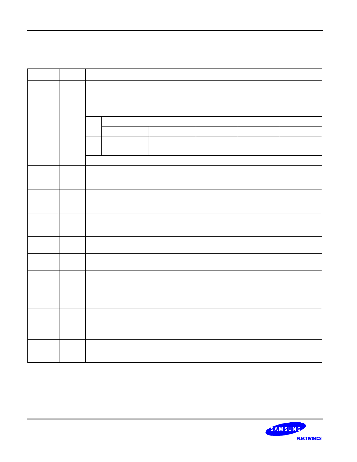
PIN DESCRIPTION
POWER SUPPLY
Table 3. Power Supply Pins
Name I/O Description
VDD Supply Power supply
VSS Supply
V0
V1
V2
V3
V4
I/O
Ground
LCD driver supplies voltages
The voltage determined by LCD pixel is impedance converted by an operational amplifier
for application.
Voltages should have the following relationship;
V0 ≥ V1 ≥ V2 ≥ V3 ≥ V4 ≥ VSS
When the internal power circuit is active, these voltages are generated as following table
according to the state of LCD bias.
LCD bias
1/N bias
NOTE: N = 4 to 11
V1
(N-1) / N x V0
V2 V3 V4
(N-2) / N x V0 (2/N) x V0 (1/N) x V0
LCD DRIVER SUPPLY
Table 4. LCD Driver Supply Pins
Name I/O Description
C1- O Capacitor 1 negative connection pin for voltage converter
C1+ O Capacitor 1 positive connection pin for voltage converter
C2- O Capacitor 2 negative connection pin for voltage converter
C2+ O Capacitor 2 positive connection pin for voltage converter
C3+ O Capacitor 3 positive connection pin for voltage converter
C4+ O Capacitor 4 positive connection pin for voltage converter
C5+ O Capacitor 5 positive connection pin for voltage converter
VOUT I/O Voltage converter input / output pin
VCI I
VR I
REF I
VEXT I
Voltage converter input voltage pin
Voltages should have the following relationship: VDD ≤ VCI ≤ V0
V0 voltage adjustment pin
It is valid only when on-chip resistors are not used (INTRS = "L")
Selects the external VREF voltage via VEXT pin
− REF = "L": using the external VREF
− REF = "H": using the internal VREF
Externally input reference voltage (VREF) for the internal voltage regulator
It is valid only when REF is "L".
7
81 COM / 104 SEG DRIVER & CONTROLLER FOR STN LCD SPEC. VER. 1.4 KS0718
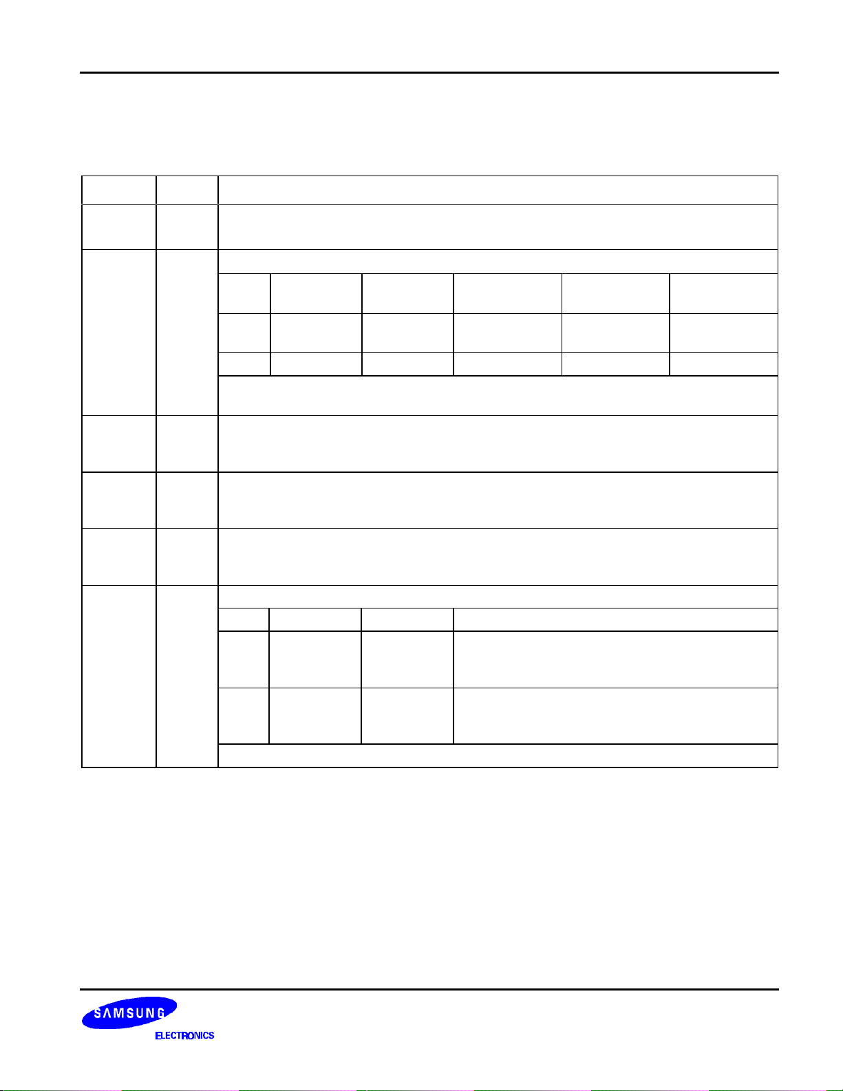
SYSTEM CONTROL
Table 5. System Control Pins
Name I/O Description
Master / slave operations select pin
− MS = "H": master operation
− MS = "L": slave operation
The following table depends on the MS status.
MS I
CL I/O
SYNC I/O
M I/O
FR O
FRS O
INTRS I
HPMB I
TEST1
to
TEST3
MS
H Enabled Enabled Output Output Output
L Disabled Disabled Input Input Input
Display clock input / output pin
When the KS0718 is used in master/slave mode (Multi-chip), the CL pins must be
connected each other.
Display sync input / output pin
When the KS0718 is used in master/slave mode (Multi-chip), the SYNC pins must be
connected each other.
LCD AC signals input / output pin
When the KS0718 is used in master/slave mode (Multi-chip), the M pins must be
connected each other.
Static driver common output pin
This pin is used together with the FRS pin.
Static driver segment output pin
This pin is used together with the FR pin.
Internal resistors select pin
This pin selects the resistors for adjusting V0 voltage level.
− INTRS = "H": use the internal resistors
− INTRS = "L": use the external resistors
VR pin and external resistive divider control V0 voltage.
Power control pin of the power supplies circuit for LCD driver
− HPMB = "L": high power mode
− HPMB = "H": normal mode
This pin is valid in master operation.
Test pins
I
Don’t use these pins.
Internal analog circuits Display timing signals
Oscillator Power supply CL SYNC M
8
KS0718 SPEC. VER. 1.4 81 COM / 104 SEG DRIVER & CONTROLLER FOR STN LCD
MICROPROCESSOR INTERFACE
Table 6. Microprocessor Interface Pins
Name I/O Description
RESETB I
PS I
C68 I
CS1B
CS2
RS I
RW_WR I
Reset the input pin
When RESETB is "L", initialization is executed.
Parallel/Serial data input select input
PS
H Parallel RS DB0 to DB7
L Serial RS SID(DB7) Write only SCLK(DB6)
*NOTE: When PS is "L", DB0 to DB5 are high impedance and E_RD and RW_WR
must be fixed to either "H" or "L".
Microprocessor interface select input pin
− C68 = "H": 6800-series MPU interface
− C68 = "L": 8080-series MPU interface
Chip select input pins
Data/instruction I/O is enabled only when CS1B is "L" and CS2 is "H". When chip
I
select is non-active, DB0 to DB7 may be high impedance.
Register select input pin
− RS = "H": DB0 to DB7 are display data
− RS = "L": DB0 to DB7 are control data
Read / Write execution control pin
C68 MPU Type RW_WR Description
H 6800-series RW
L 8080-series /WR
Interface
Mode
Data/
Instruction
Data Read / Write Serial Clock
E_RD
RW_WR
Read/Write control input pin
− RW = "H": read
− RW = "L": write
Write enable clock input pin
The data on DB0 to DB7 are latched at the rising
edge of the /WR signal.
-
9
81 COM / 104 SEG DRIVER & CONTROLLER FOR STN LCD SPEC. VER. 1.4 KS0718
Table 6 (Continued)
Name I/O Description
Read / Write execution control pin
C68 MPU Type E_RD Description
Read/Write control input pin
− RW = "H": When E is "H", DB0 to DB7 are in an
E_RD I
H 6800-series E
output status.
− RW = "L": The data on DB0 to DB7 are latched at
the falling edge of the E signal.
Read enable clock input pin
L 8080-series /RD
When /RD is "L", DB0 to DB7 are in an output
status.
8-bit bi-directional data bus that is connected to the standard 8-bit microprocessor data
DB0
to
DB7
I/O
bus. When the serial interface selected (PS = "L");
− DB0 to DB5: high impedance
− DB6: serial input clock (SCLK)
− DB7: serial input data (SID)
When chip select is not active, DB0 to DB7 may be high impedance.
10
KS0718 SPEC. VER. 1.4 81 COM / 104 SEG DRIVER & CONTROLLER FOR STN LCD
LCD DRIVER OUTPUTS
Table 7. LCD Driver Outputs Pins
Name I/O Description
LCD segment driver outputs
The display data and the M signal control the output voltage of segment driver.
SEG0
to
SEG103
COM0
to
COM79
COMS
(COMS1)
Display data M
H H V0 V2
O
LCD common driver outputs
The internal scanning data and M signal control the output voltage of common driver.
O
O
Common output for the icons
The output signals of two pins are same. When not used, these pins should be left open.
H L VSS V3
L H V2 V0
L L V3 VSS
Power save mode VSS VSS
Scan data M Common driver output voltage
H H VSS
H L V0
L H V1
L L V4
Power save mode VSS
Segment driver output voltage
Normal display Reverse display
NOTE: DUMMY – These pins should be opened (floated).
11
81 COM / 104 SEG DRIVER & CONTROLLER FOR STN LCD SPEC. VER. 1.4 KS0718
FUNCTIONAL DESCRIPTION
MICROPROCESSOR INTERFACE
Chip Select Input
There are CS1B and CS2 pins for chip selection. The KS0718 can interface with an MPU only when CS1B is "L"
and CS2 is "H". When these pins are set to any other combination, RS, E_RD, and RW_WR inputs are disabled
and DB0 to DB7 are to be high impedance. And, in case of serial interface, the internal shift register and the
counter are reset.
Parallel / Serial Interface
KS0718 has three types of interface with an MPU, which are one serial and two parallel interface. This parallel or
serial interface is determined by PS pin as shown in table 8
Table 8. Parallel / Serial Interface Mode
PS Type CS1B CS2 C68 Interface mode
H Parallel CS1B CS2
L Serial CS1B CS2
Parallel Interface (PS = "H")
The 8-bit bi-directional data bus is used in parallel interface and the type of MPU is selected by C68 as shown in
Table 9. The type of data transfer is determined by signals at RS, E_RD and RW_WR as shown in table 10.
Table 9. Microprocessor Selection for Parallel Interface
C68 CS1B CS2 RS E_RD RW_WR DB0 to DB7 MPU bus
H CS1B CS2 RS E RW DB0 to DB7 6800-series
L CS1B CS2 RS /RD /WR DB0 to DB7 8080-series
Table 10. Parallel Data Transfer
Common 6800-series 8080-series Description
RS
E_RD
(E)
RW_WR
(RW)
E_RD
(/RD)
RW_WR
(/WR)
H 6800-series MPU mode
L 8080-series MPU mode
*×
Serial-mode
*×: Don't care
H H H L H Display data read out
H H L H L Display data write
L H H L H Register status read
L H L H L Writes to internal register (instruction)
12
KS0718 SPEC. VER. 1.4 81 COM / 104 SEG DRIVER & CONTROLLER FOR STN LCD
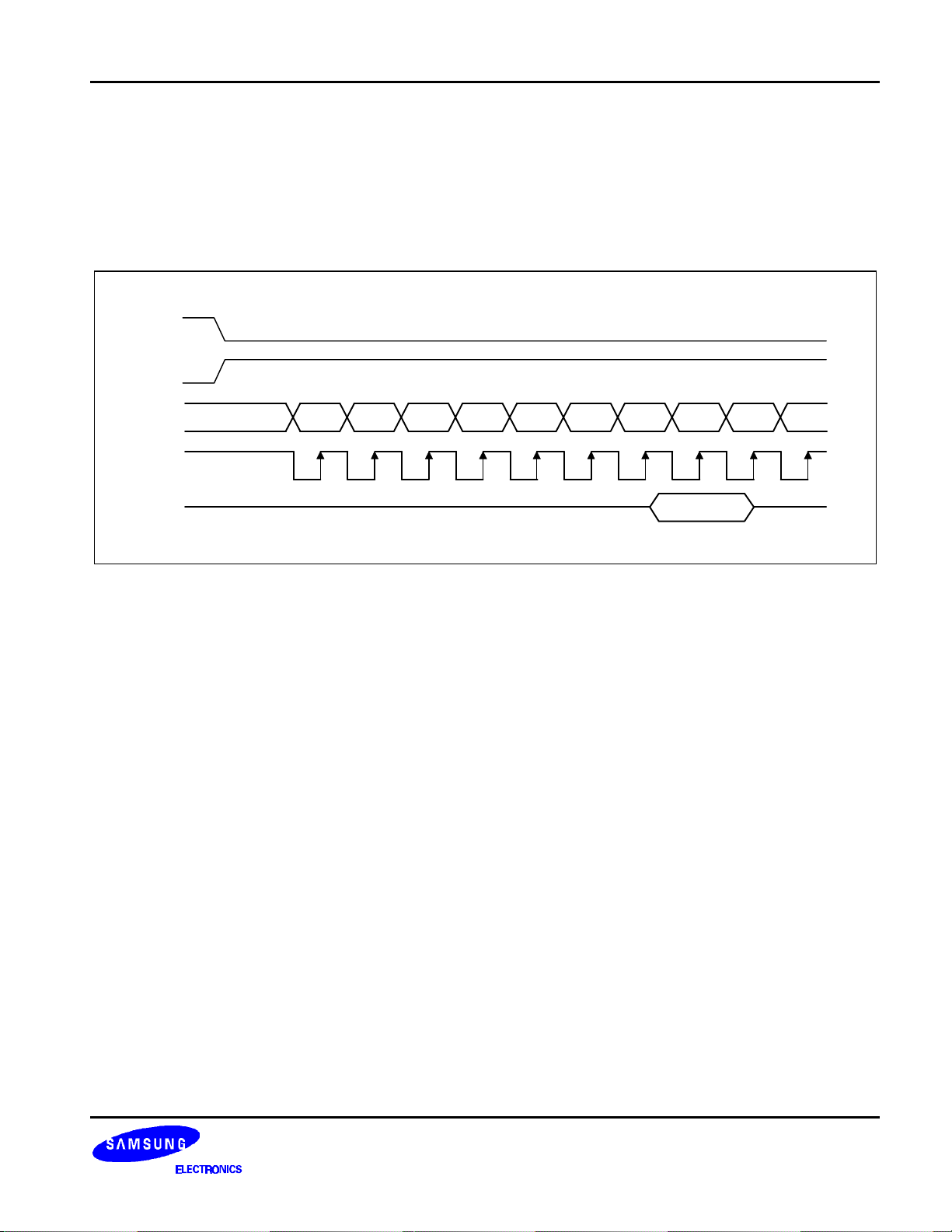
Serial Interface (PS = "L")
When the KS0718 is active, serial data (DB7) and serial clock (DB6) inputs are enabled. And not active, the
internal 8-bit shift register and the 3-bit counter are reset. Serial data can be read on the rising edge of serial clock
going into DB6 and processed as 8-bit parallel data on the eighth serial clock. Serial data input is display data
when RS is high and control data when RS is low. Since the clock signal (DB6) is easy to be affected by the
external noise caused by the line length, the operation check on the actual machine is recommended.
CS1B
CS2
SID
SCLK
RS
DB6DB7DB0DB1DB2DB3DB4DB5DB6DB7
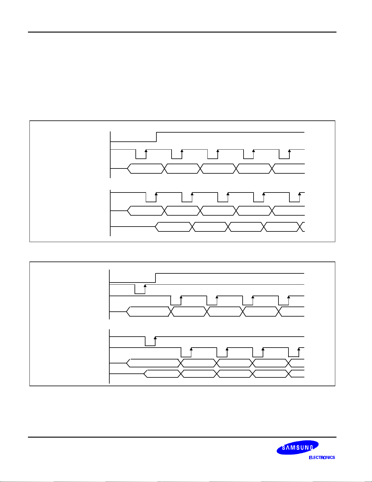
Figure 3. Serial Interface Timing
Busy Flag
The Busy Flag indicates whether the KS0718 is operating or not. When DB7 is "H" in read status operation, this
device is in busy status and will accept only read status instruction. If the cycle time is correct, the microprocessor
needs not to check this flag before each instruction, which improves the MPU performance.
13
81 COM / 104 SEG DRIVER & CONTROLLER FOR STN LCD SPEC. VER. 1.4 KS0718
D(N)
D(N+1)
D(N+2)
N
N+1
N+2
N+3
Data Transfer
The KS0718 uses bus holder and internal data bus for Data Transfer with the MPU. When writing data from the
MPU to on-chip RAM, data is automatically transferred from the bus holder to the RAM as shown in figure 4. And
when reading data from on-chip RAM to the MPU, the data for the initial read cycle is stored in the bus holder
(dummy read) and the MPU reads this stored data from bus holder for the next data read cycle as shown in figure
5. This means that a dummy read cycle must be inserted between each pair of address sets when a sequence of
address sets is executed. Therefore, the data of the specified address cannot be output with the read display data
instruction right after the address sets, but can be output at the second read of data.
MPU signals
RS
/WR
DB0 to DB7
Internal signals
/WR
BUS HOLDER
COLUMN ADDRESS
MPU signals
RS
/WR
/RD
DB0 to DB7
Internal signals
/WR
N D(N) D(N+1) D(N+2) D(N+3)
N D(N) D(N+1) D(N+2) D(N+3)
N N+1 N+2 N+3
Figure 4. Write Timing
N
Dummy D(N) D(N+1)
14
/RD
BUS HOLDER
COLUMN ADDRESS
N
Figure 5. Read Timing
KS0718 SPEC. VER. 1.4 81 COM / 104 SEG DRIVER & CONTROLLER FOR STN LCD
- -
- -
- -
- -
001
- -
0
011
- -
0
101
- -
0
000
- -
1
DISPLAY DATA RAM (DDRAM)
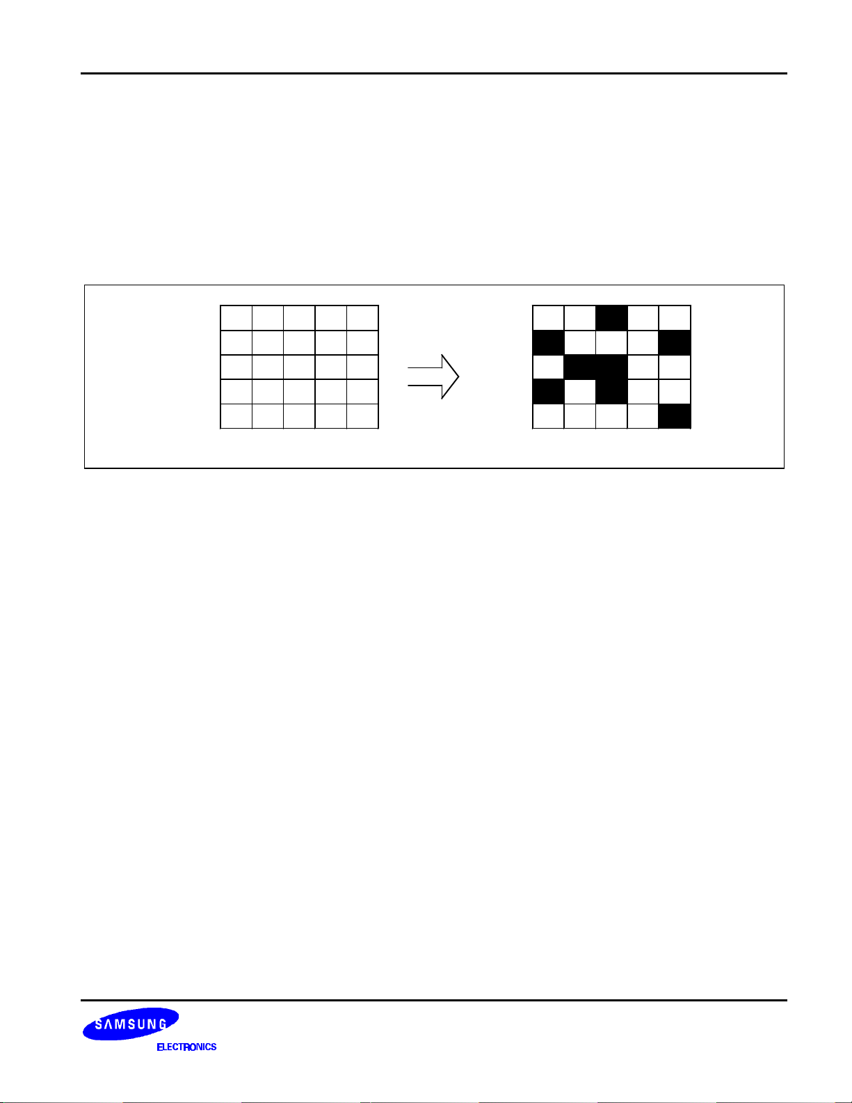
The Display Data RAM stores pixel data for the LCD. It is 89-row by 104-column addressable array. Each pixel
can be selected when the page and column addresses are specified. The 89 rows are divided into 11 pages of 8
lines and the 12th page with a single line (DB0 only). Data is read from or written to the 8 lines of each page
directly through DB0 to DB7. The display data of DB0 to DB7 from the microprocessor correspond to the LCD
common lines as shown in figure 6. The microprocessor can read from and write to RAM through the I/O buffer.
Since the LCD controller operates independently, data can be written into RAM at the same time as data is being
displayed without causing the LCD flicker.
DB0
DB1
DB2
DB3
DB4
1 0 0 - - 1
COM0
COM1
COM2
COM3
COM4
- -
Display Data RAM LCD Display
Figure 6. RAM-to-LCD Data Transfer
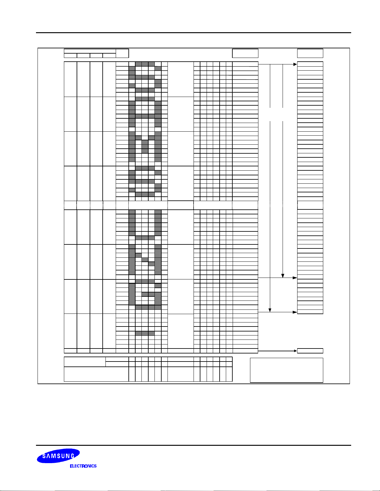
Page Address Circuit
This circuit is for providing a Page Address to Display Data RAM shown in figure 8. It incorporates 4-bit Page
Address register changed by only the "Set Page" instruction. Page Address 11 (DB3, DB1 and DB0 are "H", DB2
is "L") is a special RAM area for the icons and display data DB0 is only valid.
Line Address Circuit
This circuit assigns DDRAM a Line Address corresponding to the first line (COM0) of the display. Therefore, by
setting line address repeatedly, it is possible to realize the screen scrolling and page switching without changing
the contents of on-chip RAM as shown in figure 8 & figure 9. It incorporates 7-bit Line Address register changed
by only the initial display line instruction and 7-bit counter circuit. At the beginning of each LCD frame, the
contents of register are copied to the line counter which is increased by CL signal and generates the Line Address
for transferring the 104-bit RAM data to the display data latch circuit. However, display data of icons are not
scrolled because the MPU can not access Line Address of icons.
15
81 COM / 104 SEG DRIVER & CONTROLLER FOR STN LCD SPEC. VER. 1.4 KS0718
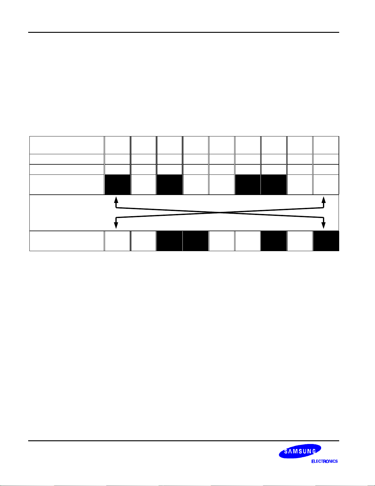
Column Address Circuit
Column address circuit has a 7-bit preset counter that provides column address to the Display Data RAM as
shown in figure 8. When set Column Address MSB / LSB instruction is issued, 7-bit [Y6:Y0] is updated. And, since
this address is increased by 1 each a read or write data instruction, microprocessor can access the display data
continuously. However, the counter is not incremented and locked if a non-existing address above 67H. It is
unlocked if a Column Address is set again by set Column Address MSB / LSB instruction. And the Column
Address counter is independent of page address register.
ADC Select instruction makes it possible to invert the relationship between the column address and the segment
outputs. It is necessary to rewrite the display data on built-in RAM after issuing ADC Select instruction. Refer to
the following figure 7.
SEG output
SEG
0
SEG
1
SEG
2
SEG
3
... ...
SEG
100
SEG
101
SEG
102
SEG
103
Column address [Y6:Y0] 00H 01H 02H 03H ... ... 64H 65H 66H 67H
Display data 1 0 1 0 1 1 0 0
LCD panel display
... ...
( ADC = 0 )
LCD panel display
( ADC = 1 )
... ...
Figure 7. The Relationship between the Column Address and the Segment Outputs
Segment Control Circuit
This circuit controls the display data by the Display ON / OFF, reverse display ON / OFF and entire display ON /
OFF instructions without changing the data in the display data RAM.
16
KS0718 SPEC. VER. 1.4 81 COM / 104 SEG DRIVER & CONTROLLER FOR STN LCD
Page Address
DB3 DB0DB1DB2
0 0 0 0
0 0 0 1
0 0 1 0
0 0 1 1
0 1 1 1
1 0 0 0
1 0 0 1
1 0 1 0
1 0 1 1
Column
Address
LCD Output
Data
ADC=0
ADC=1
DB0
DB1
DB2
DB3
DB4
DB5
DB6
DB7
DB0
DB1
DB2
DB3
DB4
DB5
DB6
DB7
DB0
DB1
DB2
DB3
DB4
DB5
DB6
DB7
DB0
DB1
DB2
DB3
DB4
DB5
DB6
DB7
DB0
DB1
DB2
DB3
DB4
DB5
DB6
DB7
DB0
DB1
DB2
DB3
DB4
DB5
DB6
DB7
DB0
DB1
DB2
DB3
DB4
DB5
DB6
DB7
DB0
DB1
DB2
DB3
DB4
DB5
DB6
DB7
DB0
00
01 02 03 04 05 62 63 64 65 66 67
SEG1
SEG0
SEG2
SEG3
SEG4
SEG5
Page 0
Page 1
Page 2
Page 3
Page7
Page8
Page9
Page10
Page 11
- - - - -
- - - - -
- - - - -
SEG99
SEG98
SEG100
SEG101
00
0102030405626364656667
SEG103
SEG102
Line
Address
00H
01H
02H
03H
04H
05H
06H
07H
08H
09H
0AH
0BH
0CH
0DH
0EH
0FH
10H
11H
12H
13H
14H
15H
16H
17H
18H
19H
1AH
1BH
1CH
1DH
1EH
1FH
38H
39H
3AH
3BH
3CH
3DH
3EH
3FH
40H
41H
42H
43H
44H
45H
46H
47H
48H
49H
4AH
4BH
4CH
4DH
4EH
4FH
50H
51H
52H
53H
54H
55H
56H
57H
register = 00H
1/81
When Initial line address = 00H
Initial line
Duty
1/73
Duty
COM
Output
COM0
COM1
COM2
COM3
COM4
COM5
COM6
COM7
COM8
COM9
COM10
COM11
COM12
COM13
COM14
COM15
COM16
COM17
COM18
COM19
COM20
COM21
COM22
COM23
COM24
COM25
COM26
COM27
COM28
COM29
COM30
COM31
COM56
COM57
COM58
COM59
COM60
COM61
COM62
COM63
COM64
COM65
COM66
COM67
COM68
COM69
COM70
COM71
COM72
COM73
COM74
COM75
COM76
COM77
COM78
COM79
COMS
Figure 8. Display Data RAM Map (Initial Line Address = 00H)
17
 Loading...