

Samsung KS0127B Datasheet

KS0127B Data Sheet
MULTISTANDARD VIDEO DECODER/SCALER
MULTIMEDIA VIDEO
The KS0127B converts analog NTSC, PAL or SECAM
video in composite, S-video, or component format to
digitized component video. Output data can be selected for
CCIR 601 or square pixel sample rates in either YCbCr or
RGB formats. The digital video can be scaled down in both
the horizontal and vertical directions. The KS0127B also
decodes Intercast, Teletext, Closed Caption, and WSS
data with a built-in bit data slicer. Digitized CVBS data can
be output directly during VBI for external processing.
FEATURES
• Accepts NTSC-M/N/4.43, PAL-M/N/B/G/H/I/D/K/L and
SECAM formats with auto detection
• 6 analog inputs: 3 S-video, 6 composite, or 1 3-wire
YCbCr component video
• 2-line luma and chroma comb filters including
adaptive luma comb for NTSC
• Programmable luma bandwidth, contrast,
brightness, and edge enhancement
• Programmable chroma bandwidth, hue, and
saturation
• High quality horizontal and vertical down scaler
• Intercast, Teletext and Closed Caption decoding with
built-in bit slicer
• Direct output of digitized CVBS during VBI for
Intercast application
• Analog square pixel or CCIR 601 sample rates
• Output in 4:4:4, 4:2:2, or 4:1:1 YCbCr component, or
24-bit or 16-bit RGB formats with dithering
• YCbCr 4:2:2 output can be 8 or 16 bits wide with
embedded timing reference code support for 8-bit
mode
• Simultaneous scaled and non-scaled digital output
ports outputs for 8-bit mode.
• Direct access to scaler via bi-directional digital port.
• Programmable Gamma correction table
• Programmable timing signals
• Industry standard IIC interface
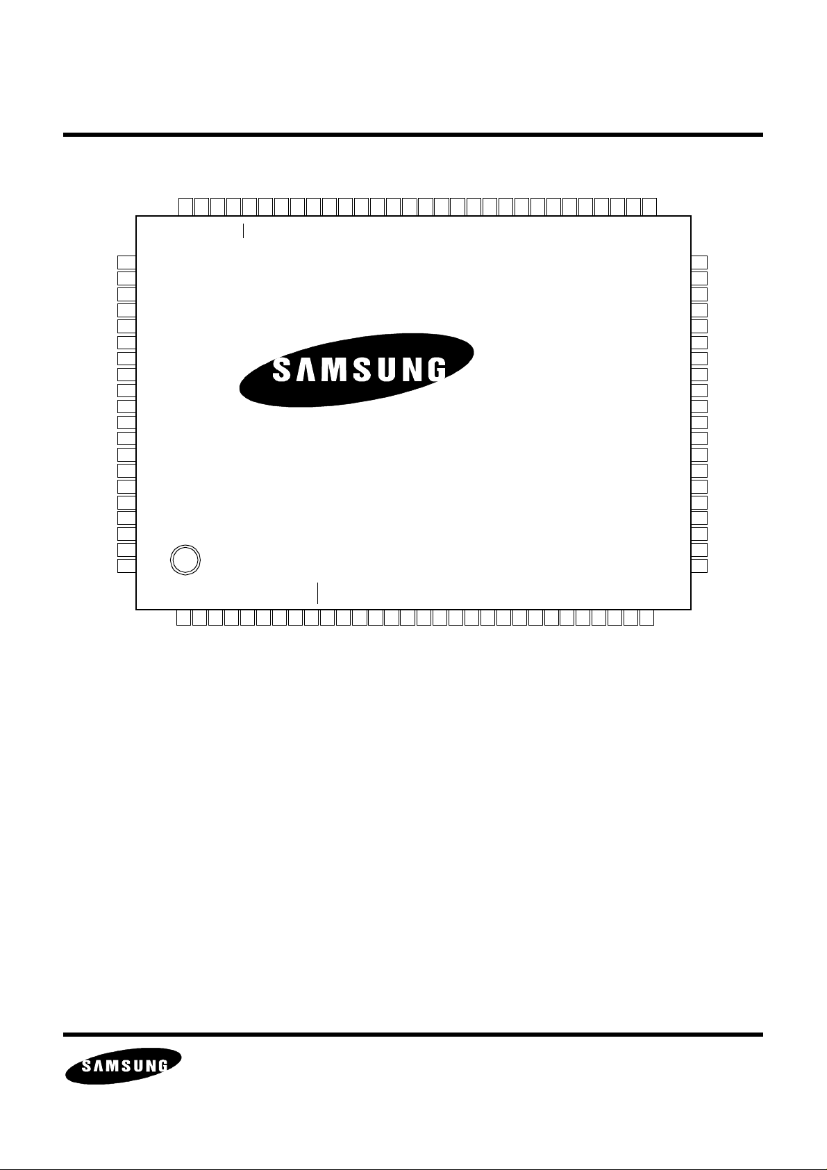
100 PQFP
ORDERING INFORMATION
Device Package Temperature Range
KS0127B 100 PQFP -20°~+70°C
APPLICATIONS
• Multimedia
• Digital Video
• Video Capture/Editing
RELATED PRODUCTS
• KS0119Q2 NTSC VIDEO ENCODER
• KS0123 MULTISTANDARD VIDEO ENCODER
• KS0125 MULTISTANDARD VIDEO ENCODER
• KS0122 MULTISTANDARD VIDEO DECODER
• KS0127 MULTISTANDARD VIDEO DECODER
ELECTRONICS
PAGE 1 OF 96Modified on May/04/2000
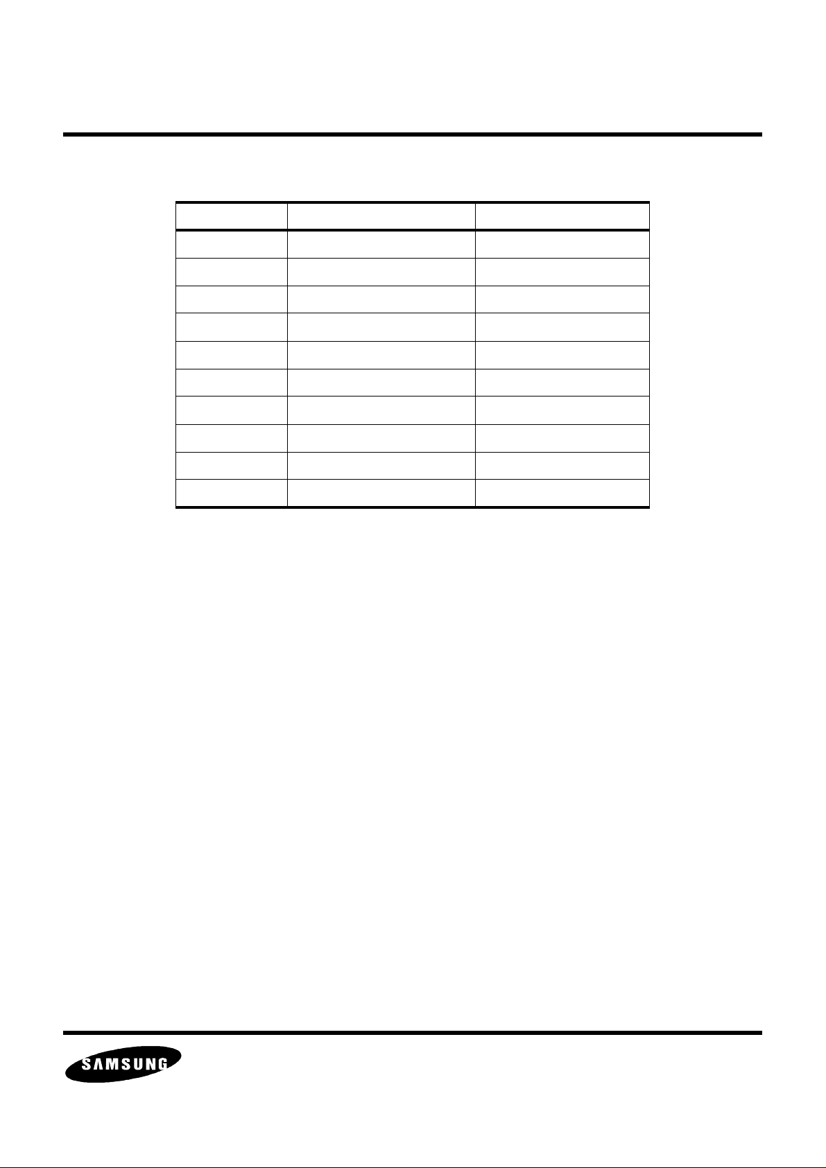
KS0127B Data Sheet MULTIMEDIA VIDEO
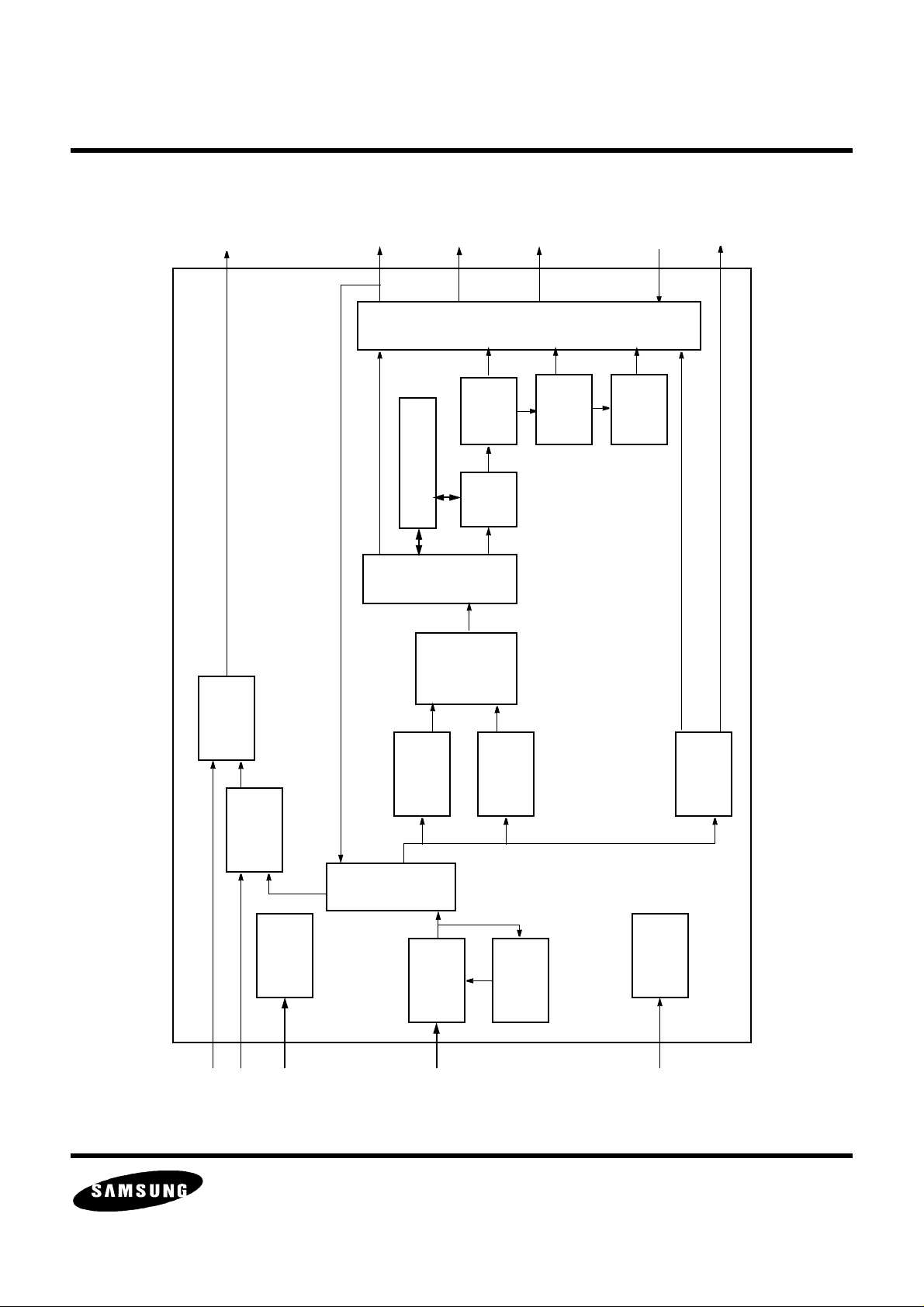
BLOCK DIAGRAM
HS1
HS2VSHAV
VAVCKCK2
SCH
PID
EHAV
EVAV
EXV[7:0]
Non Scaler Output
Y[7:0]
Data
Format
Output
Horizontal
SRAM
Vertical
C[7:0]
Color
Space
Scaler
Scaler
Converter
OEN
Gamma
LUT
CCEN
CCDAT
Comb
Filter
Variable
LPF
Sliced VBI or Raw CVBS
Line Lock,
Timing
Generation
Scaler Input OR Simultaneous Non Scaler Output OR 24-bit Output
Digital
Input
Timing
Reference
Generator/
Compensation
Luma
Processing
EXV
Control
Direct.
6 input MUX
2-AGCs
Chroma
Processing
Gain/Offset
2-ADCs
Control
VBI Data
Decoding
IIC Host
Interface
XTALI
XTALO
ELECTRONICS
HS1
VS
COMP2
VRT
VRB
AY[2:0]
AC[2:0]
Modified on May/04/2000
SCLK
SDAT
AEX1,0
PAGE 2 OF 96
KS0127B Data Sheet MULTIMEDIA VIDEO
PIN ASSIGNMENT - 100 PQFP
81
82
83
84
85
86
87
88
89
90
91
92
93
94
95
96
97
98
99
100
80 79 78 77 76 75 74 73 72 71 70 69 68 67 66 65 64 63 62 60 59 58 57 56 55 54 53 52 51
NCP
NCP
VSS
AY0
VDDA
AY1
VSS
AY2
VDDA
AC0
VSS
AC1
VDDA
AC2
VSS
TEST
COMP2
VDDA
NCP
NCP
VRT
VRB
NCP
NCP
SCLK
CCEN
HS2(IIC)
EXV7
AEX1
AEX0
SDAT
CCDAT
EXV6
KS0127B
EHAV
VSS
XTALO
XTALI
VDDA1
RST
VDD3
VAV(OENC0)
EVAV(OENC1)
NCP
NCP
1 2 3 4 5 6 7 8 9 10 11 12 13 14 15 16 17 18 19 20 21 22 23 24 25 26 27 28 29 30
VSS
VDD3
VSS
VDD3
VDD3
VSS
OEN
EXV0
VSS
EXV5
PIDCKVSS
61
VSS
VDD
EXV3
EXV4
VDD
CK2
PORTA
ODDVSSCH(PORTB)
TESTEN
Y7
HAV
HS1
NCP
NCP
NCP
50
NCP
49
Y3
48
Y2
47
Y1
46
Y0
45
C7
44
VDD3
43
VDD3
42
VSS
41
VSS
40
C6
39
C5
38
C4
37
C3
36
C2
35
34
C1
33
C0
NCP
32
NCP
31
NCP
EXV1
NCP
EXV2
Y4
Y5
Y6
ELECTRONICS
Modified on May/04/2000
PAGE 3 OF 96

KS0127B Data Sheet MULTIMEDIA VIDEO
PIN DESCRIPTION
Pin Name Pin # Type Description
INPUT
AY0 84 I 1 of 6 analog CVBS or 1of 3 S-video Y inputs.
AY1 86 I 1 of 6 analog CVBS or 1of 3 S-video Y inputs.
AY2 88 I 1 of 6 analog CVBS input or 1 of 3 S-video Y inputs or Y input for 3
wire component input
AC0 90 I 1 of 6 analog CVBS or 1 of 3 S-video C inputs.
AC1 92 I 1 of 6 analog CVBS or 1 of 3 S-video C inputs or Cb input for 3 wire
component input
AC2 94 I 1 of 6 analog CVBS or 1 of 3 S-video C inputs or Cr input for 3 wire
component input
XTALI 8 I Pin 1 for an external crystal or TTL clock input.
XTALO 7 O Pin 2 for an external crystal.
RST 10 I Chip reset. Active low signal.
OUTPUT (All output pins can be selectively three-stated)
Y0 - Y7, C0 - C7 45-48,53-56,33-
39,44
EXV0 - EXV7 16,27,28,61-63,
68,71
HS1 26 I/O Programmable horizontal timing signal. One pulse every video line.
HS2(IIC) 76 I/O Programmable horizontal timing signal. One pulse every video line.
VS 23 I/O Programmable vertical timing signal. When the EXV port is
HAV 25 O Programmable horizontal active video flag.
VAV(OENC0) 3 I/O Programmable vertical active video flag.
O Digital video outputs.
I/O Expanded digital video I/O port. Can be configured as an additional
8-bit output port (no scaling), or additional outputs of the main digital
output stream for 24 bit output modes, as an 8-bit input for direct
digital access of the down scaler.
When the EXV port is configured as an input, this pin can be
programmed as an input.
At power up, this pin needs a 10 kΩ pull-down resistor to configure
the chip to operate in IIC mode.
configured as an input, this pin can be programmed as an input.
During reset, the pin is an input and the logic state of this pin is
latched into the OENC[0] register bit. Use a 10 kΩ resistor for pull-up
or pull-down.
EHAV 5 O Valid pixel data flag. Polarity is programmable. Active when output
video data is valid.
Modified on May/04/2000
ELECTRONICS
PAGE 4 OF 96
KS0127B Data Sheet MULTIMEDIA VIDEO
PIN DESCRIPTION (Continued)
Pin Name Pin # Type Description
EVAV(OENC1) 4 I/O Valid line flag. Polarity is programmable. Active when output video
line is valid. During reset, the pin is an input and the logic state of
this pin is latched into the OENC[1]register bit. Use a 10 kΩ resistor
for pull-up or pull-down.
ODD 22 O Odd field flag. Polarity is programmable. Active for fields 1 and 3.
PID 17 O PAL ID flag. High for phase alternating line.
OEN 15 I Digital video data, timing and clock output 3-state control.
CK 18 I/O Pixel clock. In normal decoding mode, this is an output. When the
EXV port is used as an input, this can be programmed as an input
pixel clock.
CK2 21 O Pixel output clock (rate is one half of CK) aligned to HAV signal.
CCDAT 73 O Sliced VBI data output. Data can be from Closed Caption, Teletext,
Intercast, or WSS type encoded data.
CCEN 74 O When high, this pin indicates that valid VBI data is being clocked out
at the CCDAT pin or at the digital video output.
MULTI-PURPOSE I/O PORTS AND TEST ENABLE
PORTA 58 I/O Multi-purpose I/O port.
SCH(PORTB) 24 I/O Multi-purpose I/O port.
TESTEN 57 I When tied to VDD, the chip is put into the test mode. For normal use,
this pin should be connected to VSS.
TEST 96 I When tied to VDD, the chip is put into the test mode. For normal use,
this pin should be connected to VSS.
REFERENCE AND COMPENSATION
VRT 77 I/O ADC VRT compensation (requires an external 0.1 µF capacitor
connected to VSS).
VRB 78 I/O ADC VRB compensation (requires an external 0.1 µF capacitor
connected to VSS).
COMP2 97 I/O Internal 1.3 V reference (requires an external 0.1 µF capacitor
connected to VSS).
HOST INTERFACE
SCLK 75 I Serial clock for IIC host interface.
SDAT 72 I/O Serial data for IIC host interface.
AEX0 - AEX1 69 - 70 I Device ID selection for IIC host interface.
Modified on May/04/2000
ELECTRONICS
PAGE 5 OF 96

KS0127B Data Sheet MULTIMEDIA VIDEO
PIN DESCRIPTION (Continued)
Pin Name Pin # Type Description
POWER AND GROUND
VDD 20,59 PWR Digital power supply for output buffers. The voltage can be +5V or
3.3V depending on interface requirement.
VDD3 11,12,42,43,66,67+3.3V Digital power supply for internal logic.
VDDA 85,89,93,98 +5V Analog power supply for ADC, AGC and reference circuits.
VDDA1 9 +5V Analog power supply for clock generation circuitry.
VSS 6,13,14,19,40,
41,60,64,65,83,
87,91,95
NC
NCP 1,2,29-32,49-52,
79-82,99,100
GND Common ground.
- These pins are directly connected to the die substrate. If electrical
connect is desired (not required) only connection to VSS is allowed.
ELECTRONICS
Modified on May/04/2000
PAGE 6 OF 96
KS0127B Data Sheet MULTIMEDIA VIDEO
PIN CROSS REFERENCE: NUMERICAL ORDER BY PIN NUMBER
Pin # Pin Name Pin # Pin Name Pin # Pin Name Pin # Pin Name
1 NCP 26 HS1 51 NCP 76 HS2(IIC)
2 NCP 27 EXV1 52 NCP 77 VRT
3 VAV(OENC0) 28 EXV2 53 Y4 78 VRB
4 EVAV(OENC1) 29 NCP 54 Y5 79 NCP
5 EHAV 30 NCP 55 Y6 80 NCP
6 VSS 31 NCP 56 Y7 81 NCP
7 XTALO 32 NCP 57 TESTEN 82 NCP
8 XTALI 33 C0 58 PORTA 83 VSS
9 VDDA1 34 C1 59 VDD 84 AY0
10 RST 35 C2 60 VSS 85 VDDA
11 VDD3 36 C3 61 EXV3 86 AY1
12 VDD3 37 C4 62 EXV4 87 VSS
13 VSS 38 C5 63 EXV5 88 AY2
14 VSS 39 C6 64 VSS 89 VDDA
15 OEN 40 VSS 65 VSS 90 AC0
16 EXV0 41 VSS 66 VDD3 91 VSS
17 PID 42 VDD3 67 VDD3 92 AC1
18 CK 43 VDD3 68 EXV6 93 VDDA
19 VSS 44 C7 69 AEX0 94 AC2
20 VDD 45 Y0 70 AEX1 95 VSS
21 CK2 46 Y1 71 EXV7 96 TEST
22 ODD 47 Y2 72 SDAT 97 COMP2
23 VS 48 Y3 73 CCDAT 98 VDDA
24 SCH(PORTB) 49 NCP 74 CCEN 99 NCP
25 HAV 50 NCP 75 SCLK 100 NCP
ELECTRONICS
Modified on May/04/2000
PAGE 7 OF 96

KS0127B Data Sheet MULTIMEDIA VIDEO
1. FUNCTIONAL DESCRIPTION
1.1. VIDEO INPUT
The KS0127B supports complete video decoding of many analog video standards. In addition, the chip can support
direct 8-bit YCbCr input for high quality video scaling and other processing.
1.1.1. Analog Video Input
Figure 1 shows the detailed block diagram of the analog front end. Up to six composite video sources, three
S-video sources, one 3-wire YCbCr component video source, or any combination can be selected. The allowed
inputs are selected using the INSEL[3:0] bits in the CMDB register. Table 1 lists all possible input selections. The
front end has two paths each containing an analog gain control, a clamping control, and an 8-bit ADC. Composite
video input uses only the luma path. S-video and analog component YCbCr inputs utilize both the luma and
chroma paths. The ADC digital data is used to calculate the correct gain and clamp values. The data is feedback to
the analog clamping and gain control. This architecture eliminates any offset and gain mismatch in the analog front
end.
OFFSET
VRT
VRB
LPF
LPF
To Chroma Processing
To Luma Processing
To Timing Generation
AC0
AC1
AC2
AY0
AY1
AY2
MUX
MUX
8-bit
Digital
Input
AGC
AGC
8 Bit ADC
COMP1
8 Bit ADC
GAIN
OFFSET
Figure 1. Analog Front End
The analog inputs must be AC coupled through an external 0.1 µF capacitor clamp. Due to the high sampling rate
of the ADC’s inside the KS0127B, most video sources will not require a low-pass filter for alias reduction. For those
video sources with harmonics above 13 MHz, a simple single order pole at 6 MHz will provide sufficient high
frequency signal reduction. This can be implemented with a 400 pF capacitor in parallel with the 75 Ω load.
Analog
Video
0.1 µF
75 Ω
KS0127B
ELECTRONICS
Figure 2. Typical Analog Video Input
Modified on May/04/2000
PAGE 8 OF 96
KS0127B Data Sheet MULTIMEDIA VIDEO
Table 1: Analog Video Input selections
INSEL[3:0](hex) Selected Input(s) Video Type
0 AY0 Composite
1 AY1 Composite
2 AY2 Composite
4 AC0 Composite
5 AC1 Composite
6 AC2 Composite
8 AY0, AC0 S-Video
9 AY1, AC1 S-Video
A AY2, AC2 S-Video
F AY2(Y), AC1(Cb), AC2(Cr) YCbCr component video
1.1.2. Digital AGC Control
The AGC normally references to the ADC code difference between sync tip and back porch. Two sets of sync
tip-back porch ADC values are available for different AGC gain requirements: if AGCGN = 0, the sync tip locks to
code 2, and the back porch locks to code 70; when AGCGN = 1, the sync tip locks to 16, and the back porch locks
to code 70. Video signal with abnormal sync tip or very bright saturated colors may cause the ADC to limit the
maximum value. This situation can be corrected by enabling the AGCOVF bit in the CMDB register to force the
gain tracking loop to reduce AGC when maximum limiting conditions occur. The AGC may also be programmed to
freeze the AGC at the current value by setting the AGCFRZ bit in the CMDB register. Once the AGC is frozen, the
gain can be manually adjusted with the AGC register. The tracking time constant for the AGC can be controlled
with the AGC_LPG[1:0] bits in the TRACKB register. In addition, the AGC tracking time constant can be
configured as 2X faster during acquisition via the AGC_LKG.
1.1.3. Digital Video Input
The high quality digital video down scaler in the KS0127B can be directly accessed via the EXV bi-directional port.
The KS0127B accepts CCIR 656 compliant 8-bit YCbCr digital video input with embedded or external timing. Video
timing may also be generated by the KS0127B. Data path for 8-bit YCbCr input is shown in Figure 3. Selection of
analog video input or digital CCIR 656 data is with the INPSL[1:0] register bits. The KS0127B can operate in
master or slave timing mode when the chip is programmed for digital video input.
1.1.4. Pixel Clock and Timing Mode Selection for Digital Video Input
Pixel clock and synchronization timing can be individually selected to either come from an external generator or be
generated internally. In addition, if synchronization is provided by an external source, the KS0127B supports
embedded syncs as defined in CCIR 656, or TTL HS and VS inputs. Selection of pixel clock is via CKDIR bit in
Modified on May/04/2000
ELECTRONICS
PAGE 9 OF 96
KS0127B Data Sheet MULTIMEDIA VIDEO
CMDD register. Timing selection is through either SYNDIR or EAV bit.
HS1
VS
EXV[7:0]
From Luma ADC
From Chroma ADC
Timing
Control
Data
Demux
Luma
Y
C
Processing
Chroma
Processing
To Luma Scaler
To Chroma Scaler
Figure 3. 8-bit YCbCr Input Data Path
By using an external pixel clock, the reference clock input at XTALI is no longer required. Additional register bits
have to be programmed for different selections of pixel clock and timing, which are detailed in Table 2. The
following register/bit-settings are required for digital video input:
INSEL[3:0] = 8, 9, A, or F.
TSTCGN = 1.
DMCTL[1:0] = 2 or 3.
UGAIN = 238.
BRT = 34.
SAT = 229.
RGBH = UNIT = PED = 1.
Table 2: Digital Video Input Pixel Clock and Timing Selection
Pixel Clock TTL Timing
CKDIR
*1
SYNDIR
0 0 0 1 0 1 3 0 if input
0 0 1 0 1 1 3 1
0 1 0 0 1 1 1 1
1 0 0 1 0 1 3 1
1 0 1 0 1 1 1 1
1 1 0 0 1 1 1 1
*1
: CKDIR = 0 - CK is output and is internally generated. CKDIR = 1 - CK is input from an external source.
*2
: SYNDIR = 0 - HS1 and VS are output. SYNDIR = 1 - HS1 and VS are inputs from external sources.
*3
: EAV = 0 - chip will not sync to embedded timing. EAV = 1 - chip will sync to embedded timing.
Note: the combination X11 for CKDIR, SYNDIR, EAV is not valid.
ELECTRONICS
Embedded
Timing
*2
EAV
Additional Register Programming
*3
VMEN TSTGPH TSTGEN TSTGFR PIXSEL MNFMT IFMT
1 0 if input
data is at
square
pixel
rate.
1 if input
is at
CCIR
601 rate.
Modified on May/04/2000
PAGE 10 OF 96
is 50 Hz
video.
1 if input
is 60 Hz
video.
KS0127B Data Sheet MULTIMEDIA VIDEO
When in digital input mode, all programmable timing registers (such as HAVB,HAVE, HS2B etc.) are still functional.
If HS1 and VS are programmed as inputs, the associated output timing controls such as HS1B,E will have no
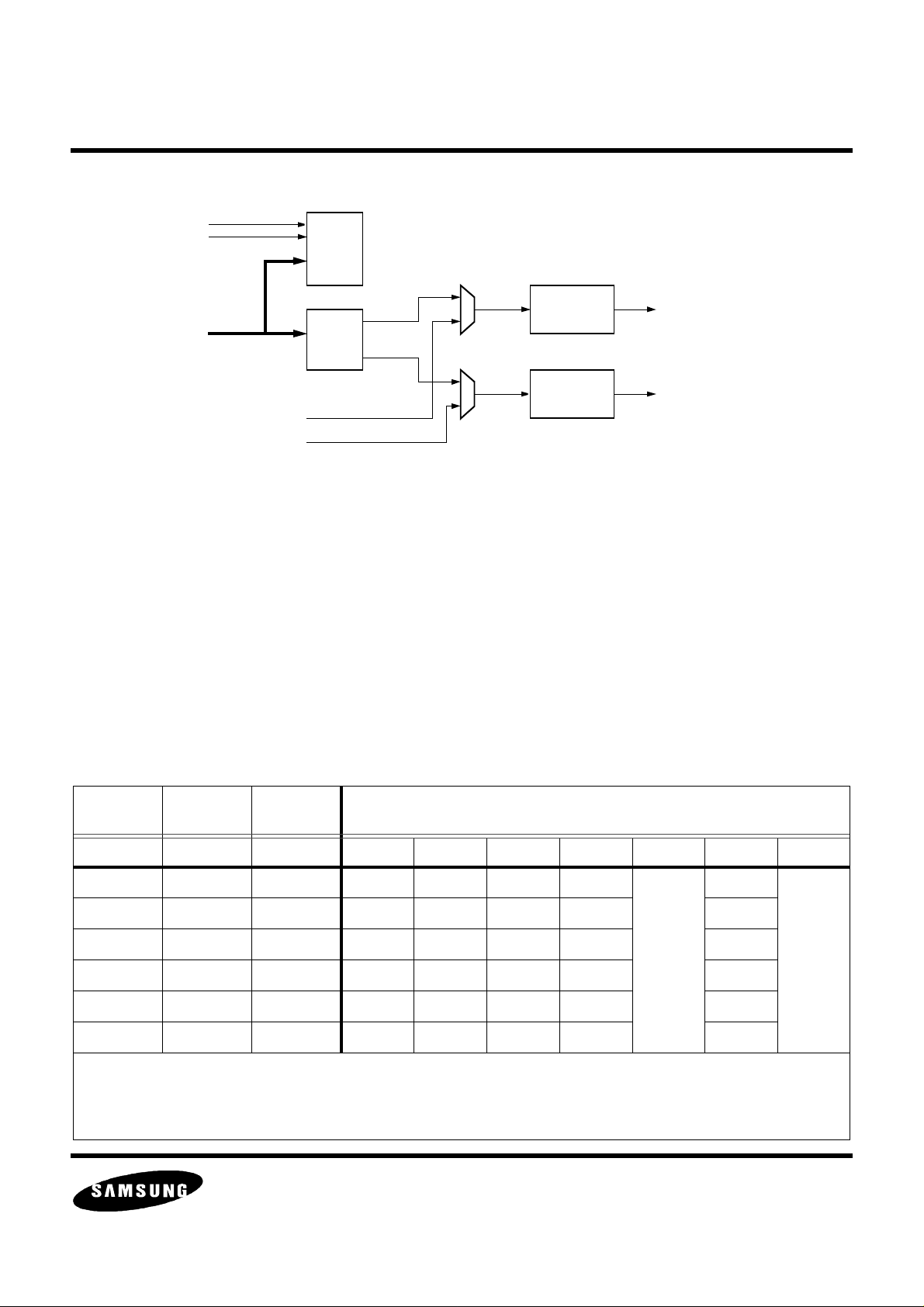
effect. An example of horizontal timing for digital input is shown in Figure 4.
HS1
Programmable, when an
output - Any input phase
is acceptable
This HS1 location can also come
From a 656 SAV code
Constant to internal counter reference
EXV[7:0]
80 10 80 10 80 10 U0Y0V0Y1U2Y2V2Y3U4Y4V4Y5U6Y6V6Y7UxYxVxYxUxYxVxYxV
Y[7:0]
Y output for OFMT=2 is
shown, any 8 or 16 bit
output format is allowed.
HAV
CK
CK2
CK can be input or output
Data group delay through chip --
80 10 80 10 80 10 U0Y0V0Y1U2Y2V2Y3U4Y4V4Y5U6Y6V6Y7UxYxVxYxU
Fully programmable HAVB location
based on internal counter
HAV -- fully programmable,
Defines location of first, last pixel
and defines Cb,Y,Cr data location
The CK2 output clock phasing
is aligned to the HAV leading
edge
Figure 4. Horizontal Timing for EXV Port as Digital Input
x
x
Fully programmable
HAVE location
1.1.5. Additional Information for Analog Component Video Input
For the KS0127B to correctly set the V component phase in analog component video input mode, PID (pin 17) and
PORTA (pin 58) need to be connected together. PORTA has to be configured as input (DIRA = 0) and connected
to the internal CBG signal (DATAA[2:0] = 3).
It is also recommended that external clamp circuit be used for Cb and Cr inputs (before the coupling caps) and the
internal chroma clamp be disabled (COFFENB = 1) due to slight Cb/Cr leakage.
Modified on May/04/2000
ELECTRONICS
PAGE 11 OF 96
KS0127B Data Sheet MULTIMEDIA VIDEO
1.2. VIDEO TRACKING AND TIMING GENERATION
When the KS0127B is configured for analog video input, the chip tracks the video input and generates a sampling
clock that is line locked to the input video. The KS0127B requires an external reference clock for video tracking.
This reference can be supplied via a crystal using the on chip crystal interface or any TTL compatible source.
These configurations are shown in Figure 5
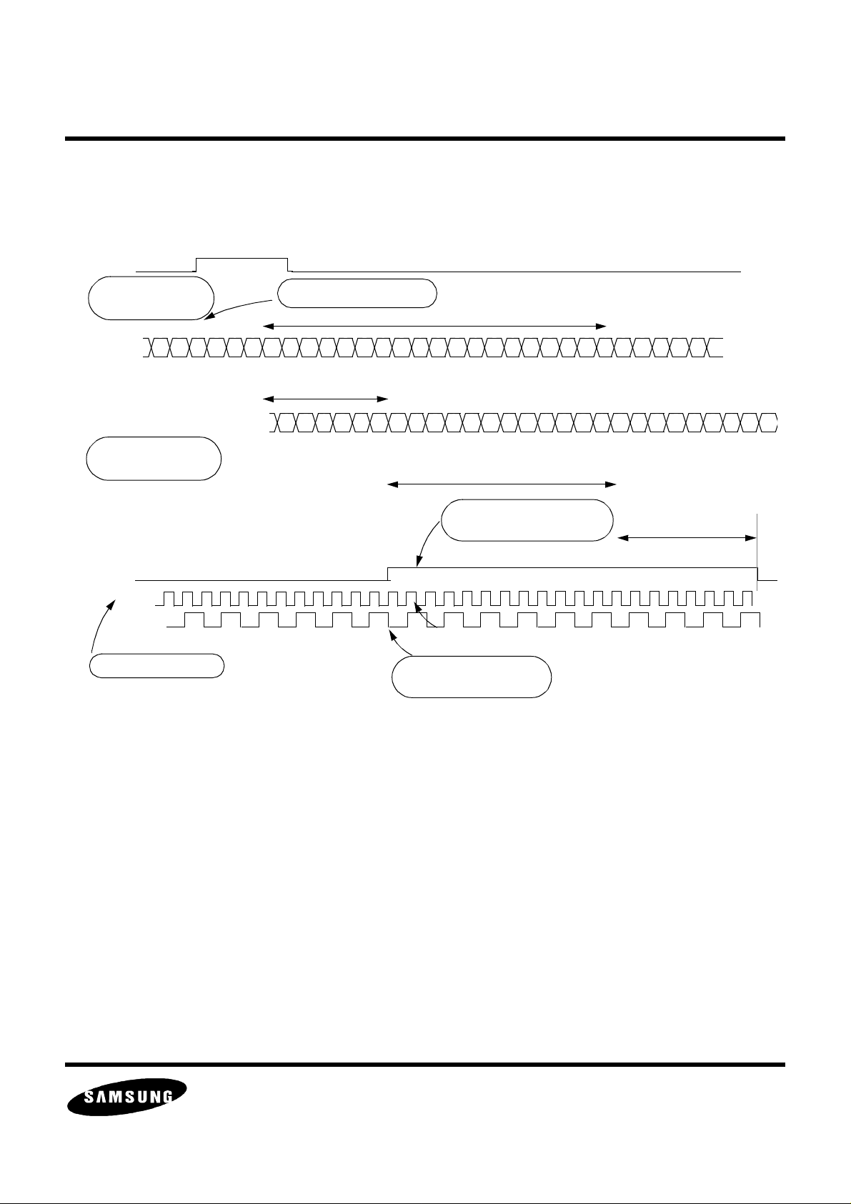
1.2.1. Clock Input Timing Reference
The KS0127B can use either a 24.576 MHz or a 26.8 MHz reference. However, it is recommended that the 24.576
MHz reference be used for CCIR 601 operation, and the 26.8 MHz reference be used for square pixel or dual mode
operation. Other specifications for the crystal are:
• Fundamental or third overtone
• Load capacitance of ~20 pF
• Series resistance of 40 Ω or less
• Frequency deviation of 50 ppm or less over operating temperature range
Optional for 3rd
harmonic crystal
22 pF
22 pF
24.576 MHz
5.7 µH
391 pF
8
XTALI
KS0127B
7
XTALO
Using a Crystal
24.576 MHz
TTL Clock
Using a Clock
N. C.
8
7
XTALI
KS0127B
XTALO
Figure 5. Standard Clock Configurations
1.2.2. The Sampling Clock
The sampling clock is generated by multiplying the line rate by N. This ensures that samples are aligned
horizontally, vertically and in time. The required N factor for the KS0127B is based upon the field rate (60 Hz or 50
Hz) and the desired sampling rates (CCIR 601 or square pixel). Field rate can be automatically detected and can
be monitored with the FFRDET bit in the STAT register. Manual control of the field rate can be controlled with the
MNFMT and IFMT bits. The PIXSEL bit in register CMDA selects CCIR 601 or square pixel. Table 3 shows the
constants for the various combinations of input formats and output pixel rates.
ELECTRONICS
Modified on May/04/2000
PAGE 12 OF 96

KS0127B Data Sheet MULTIMEDIA VIDEO
Table 3: Timing for Different Pixel Rates
CCIR 601 Data Rates Square Pixel Data Rates
M N,B,G,H,I,D,K,K1,L M N,B,G,H,I,D,K,K1,L
Units
Field Rate 60 50 60 50 Hz
Pixels/Line (N) 858 864 780 944 Pixels
Active Pixels/Line 720 720 640 768 Pixels
Active Lines/Frame 480 580 480 580 Lines
Pixel Rate 13.5 13.5 12.27 14.75 MHz
ADC Sampling Rate 27 27 24.54 29.5 MHz
The time constants for the pixel clock tracking loop can be adjusted with the HFSEL[1:0] bits.
In addition to providing the pixel clock, the KS0127B also outputs various timing signals to indicate the beginning of
a line, a field, and for field and frame identification. All the timing and clock pins may be optionally put into high
impedance state. Three-state of these pins are software controlled and initial state of these pins at power up is
controlled via two configuration pins: 3 and 4.
The KS0127B can generate all the video timing without video input. This enables the KS0127B to be used as a
video timing generator for a system that contains both the KS0127B for live video input and a MPEG decoder
which requires a video timing generator.
1.2.3. Horizontal Timing
The KS0127B creates many internal timing signals aligned to the horizontal sync tip (mid-way of the falling edge of
horizontal sync, typically ADC code 36). These include locations of color burst (CBG, CBGW) used in chrominance
processing, back porch (BPG), and sync tip timing signals (SLICE, FS_PULSE) used for AGC and clamp functions.
SLICE is low whenever the input is below half way level of horizontal sync (typically ADC code 36). FS_PULSE is
a single clock pulse coincide with the start of SLICE. One of these internal signals can be made available at the
PORTA or PORTB pin at any time.
The chip outputs two horizontal synchronization signals: HS1 and HS2. The start and stop locations for these
signals are fully programmable. Offset programmed to HSxB, HSxE, and HSxBE0 are added to the default edge
locations as shown in Table 4. Note that there are different modulo numbers for different input video standards and
output pixel rates.
Modified on May/04/2000
ELECTRONICS
PAGE 13 OF 96

KS0127B Data Sheet MULTIMEDIA VIDEO
Table 4: Horizontal Timing Signal Edge Locations (in # of CK)
60 Hz 50 Hz
Description Signal
Chip delay 120 120 120 120
Sync gate (1-CK pulse) SYG 72 72 72 72
Back porch gate BPG [147 222] [129 204] [154 234] [168 254]
Color burst gate (1-CK pulse) CBG 222 204 234 254
Wide color burst gate CBGW [159 254] [147 233] [173 254] [186 277]
CCIR 601
(modulo 1716)
Square Pixel
(modulo 1560)
CCIR 601
(modulo 1728)
Square Pixel
(modulo 1888)
Two pulses per line (1-CK each
pulse)
Default one pulse per line HS1 [65 238] [45 220] [69 250] [65 270]
Default one pulse per line HS2 [65 238] [45 220] [69 250] [65 270]
Default horizontal cropping HAV [351 75] [334 58] [379 91] [415 59]
An additional signal, HAV, is provided for horizontal video cropping. This signal has programmable polarity, start
and stop locations. Two 11-bit registers, HAVB and HAVE, are used to define the first and last pixel locations of
the horizontal portion of the cropped video. Numbers programmed into these registers are used as offset to the
default locations as shown in Table 4. Note that even though HAVB and HAVE have 1-CK resolution, the
difference between them should be maintained at multiple of 4 CKs for correct output.
Table 4 shows the default edge locations relative to the midway of the falling edge of the analog horizontal sync.
Note the numbers shown are in multiple of CK clocks. Figure 6 shows the approximate locations for the horizontal
timing signals. Horizontal timing signals used for scaling will be described in Section 1.6.1.
FH2 42, 900 42, 822 42, 906 42, 986
ELECTRONICS
Modified on May/04/2000
PAGE 14 OF 96

KS0127B Data Sheet MULTIMEDIA VIDEO
Analog video input
Digital video output
HAV
HS1,2
FS_PULSE
SLICE
SYG
BPG
CBG
CBGW
FH2
Chip delay
HAVE
HSE
HSB
Blank
HAVB
Active videoActive video
Figure 6. Approximate Locations for the Horizontal Timing Signals
1.2.4. Vertical Timing
The vertical timing signals include VS, VAV, ODD, SCH, and PID.
The VS is used for identifying the first line of video in the vertical position. The VS leading edge can be
programmed to either track the incoming video’s serration pulses or to be aligned to the beginning of the video line
or half way, as shown in Figure 36 and Figure 37. If VALIGN = 0, the VS leading edge is based on the output of an
internal low pass filter, and its location is dependent on the noise conditions of the video input. The trailing edge of
VS is locked to either the beginning of the video line or half way. The half way location relative to the beginning of
the video line changes depending on current input standard and output format. If VALIGN = 1, the leading edge of
the VS is aligned to the beginning of the video line or half way. The trailing edge is always aligned to the beginning
of the video line. The VSE bit in the CMDA register can be programmed to shorten the VS falling edge by one
horizontal line.
The VAV signal is used for vertical cropping. The start and stop lines for VAV are programmable through the VAVB
and VAVE registers, respectively.
The ODD signal signifies the current field number. When ODD is active, the current field is 1 or 3 (or 5 or 7 if in PAL
mode). The leading and trailing edges of ODD can be aligned to either the leading edge of VS (VALIGN = 1) or the
trailing edge of VS (VALIGN = 0). The signal may be used in conjunction with SCH and PID to exactly identify the
Modified on May/04/2000
PAGE 15 OF 96
ELECTRONICS

KS0127B Data Sheet MULTIMEDIA VIDEO
current field. To distinguish between fields 1, 2 verse fields 3, 4 (or fields 1, 2, 3, 4 verse fields 5, 6, 7, 8 for PAL)
the phase of the color burst relative to the sync tip must be measured. That information is provided by the SCH pin.
The KS0127B provides the output of a comparator that measures whether the current color burst phase relative to
the falling edge of the sync is greater or less than a predetermined constant. This constant is controlled with
SCHCMP[3:0]. The polarity of the SCH output pin depends on the current SCHCMP[3:0] value. The SCH signal
changes every video line. The SCH for line 260 is held for the entire vertical blanking period. By using the SCH
signal for the same line from each field, proper field identification can be determined. Figure 8 shows field
identification values for SCHCMP[3:0]=0. It is important to note that the SCH value is only valid for video signals
that have a constant sync tip to color burst relationship. This is not the case with consumer VCRs.
.
HS1
(default)
ODD FIELD and VALIGN = 0
VS
ODD
60 Hz - CCIR 601 = 885, Square = 708
50 Hz - CCIR 601 = 891, Square = 971
0, except 60 Hz Square = 2
EVEN FIELD or VALIGN = 1
VS
0, except 60 Hz Square = 2
ODD
VAV
HAV default width for each input standard and output mode
EVAV
Note: Numbers shown are in CK. Active high polarities are used. Timing shown for VAV and EVAV are with qualifier off.
27, except 60 Hz Square = 28
15, except 60 Hz Square = 14
60 Hz - 261
50 Hz - CCIR 601 = 273, Square = 341
Figure 7. Short Term Vertical Timing
ELECTRONICS
Modified on May/04/2000
PAGE 16 OF 96
KS0127B Data Sheet MULTIMEDIA VIDEO
VS
ODD
1
2
3 4
SCH
Truth Table
FIELD
ODD
SCH
1 2
H L
H L L H
3 4
H L
Note:
ODD and SCH are
measured at the trailing
edge of VS.
Figure 8. NTSC Vertical Timing Signals
The PID pin is used to identify whether the current V-axis is inverted in PAL mode. This signal changes at the color
burst. By noting this value at the same line of each field, a determination of whether a field is from {1-4} or {5-8} can
be made. As with the SCH pin, the KS0127B is designed to hold the line 260 PID measurement for the entire
vertical blank period. This allows easy sampling of the PID or current field identification.
The ODD, SCH and PID signals change at different times and more than once within the video fields. Proper data
for field identification is determined by latching all three signals at the trailing edge of VS. Figure 9 shows the VS,
ODD, SCH, and PID signals and their latched values for each of the 8 possible fields. Figure 10 is the line to line
timing diagram for these signals in PAL mode.
VS
ODD
SCH
PID
Truth Table
FIELD
ODD
SCH
PID H L
1 2
H L H L
H L
1
2
3 4
H L
L H
3 4
5 6
H L H L
L H
H L
5
7 8
L L
L H
6
7
Note:
ODD, SCH and PID are
measured at the trailing
edge of VS (VALIGN = 0).
8
Figure 9. PAL Vertical Timing Signals
Modified on May/04/2000
PAGE 17 OF 96
ELECTRONICS
KS0127B Data Sheet MULTIMEDIA VIDEO
SCH
ODD
PID
VS
HS
Figure 10. Line to Line VS, SCH and PID Timing (PAL input)
1.3. HORIZONTAL LUMA PROCESSING
A simplified block diagram for the luma path is shown in Figure 11.
Programmable
Low Pass Filter
HYLPF
Brightness
Control
FROM ADC
Contrast
Control
Decimation
Filter
HYBWR CTRAP
HYBWI
Horizontal
Peaking
HYPKCONT BRT
Chroma
Trap
Figure 11. Horizontal Luma Processing Unit
1.3.1. Luminance DC Gain
The KS0127B can accommodate CCIR 624 M/N/H/G standards, which fall into categories of -40 or -43 sync tip
and inclusion or exclusion of 7.5 setup. The KS0127B can produce correct CCIR 601 luminance output levels by
controlling the gain and offset in the luminance path via PED. This register should be set for the appropriate input
standard. The programmable CONT and BRT registers provide the user with additional flexibility to create
non-standard luminance gain and offset values.
ELECTRONICS
Modified on May/04/2000
PAGE 18 OF 96
KS0127B Data Sheet MULTIMEDIA VIDEO
Max Input
Peak White
Black Level
Blanking Level
Sync Tip
Figure 12. Luminance Signal
Luminance levels produced by the KS0127B for different broadcast standards (assuming AGCGN=0, CONT=0
and BRT=0) are summarized in Table 5.
Table 5: Luminance Digital Level Code
M/N PED=1 M/N PED=0 B/G/H PED=1
Signal
Level
(IRE)
ADC
(CVBS)
Y[7:0]
Level
(IRE)
ADC
(CVBS)
Y[7:0]
Level
(IRE)
ADC
(CVBS)
Y[7:0]
Max Input 109 255 255 109 255 255 117 255 255
Peak White 100 240 235 100 240 235 100 229 235
Black 7.5 83 16 0 70 16 0 70 16
Blank 0 70 1 0 70 16 0 70
Sync -40 2 1 -40 2 1 -43 2
KS0127B Data
Path Equation
CY1.37CVBS100–=
CY1.288CVBS74–=
CY1.37CVBS80–=
When digital component output is desired in RGB mode, the RGBH register can be programmed to increase the
0-100% values from standard CCIR 601 levels to full range levels.The gain variations are shown in Table 6.
Table 6: RGB Output Range
RGB normal gain (RGBH=0) RGB high gain (RGBH=1)
Signal Cy RGB (U,V=0) Cy RGB (U,V=0)
Peak White 235 235 255 255
Black 16 16 0 0
Modified on May/04/2000
ELECTRONICS
PAGE 19 OF 96

KS0127B Data Sheet MULTIMEDIA VIDEO
For CCIR 601 digital video input (INPSL[1:0] = 1), register UNIT must be set to 1 to produce unit gain.
1.3.2. Horizontal Luma Frequency Shaping
The luma path contains many programmable filters for different purposes. The combination of these filters will give
different frequency characteristics.
The over sampled video data from the ADC pass through a decimation filter. The decimation filter has user
programmable bandwidth. Three registers are used to control the decimation filter characteristics and each is
designed for certain purposes. The HYBWI, when set to “1”, provides extra bandwidth for very high quality video
source. The HYBWR, when set to “1”, reduces the bandwidth so high frequency noise can be eliminated. The 3-bit
register HYLPF[2:0] provides the necessary bandwidth reduction for horizontal scaling. When all three registers
are programmed to “0”, the decimation filter has the bandwidth of the normal video. The KS0127B provides the
option of bypassing the decimation filter. This option should be used only when the input video is band limited and
with low high frequency noise.
For composite video input, the notch filter can be enabled (CTRAP set to “1”) to extract the luminance. The notch
filter has different center frequencies for different input video format. User selectable peaking function is included
for edge enhancement. The notch filter should be bypassed for S-video and component video input, or if luma
comb filter is enabled.
The luminance filter characteristics have been designed to be very similar for all combinations of 60/50 Hz video
and CCIR 601/square pixel sampling rates. Figure 13 and Figure 14 show the output characteristics of the
luminance path with different filter combinations for the supported input standards and output pixel rates.
ELECTRONICS
Modified on May/04/2000
PAGE 20 OF 96
KS0127B Data Sheet MULTIMEDIA VIDEO
Figure 13. Medium to High Frequency Luma Filter Characteristics (CTRAP=0)
Figure 14. Medium to Low Frequency Luma Filter Characteristics (NTSC, CTRAP=1)
Modified on May/04/2000
ELECTRONICS
PAGE 21 OF 96

KS0127B Data Sheet MULTIMEDIA VIDEO
Figure 15. Medium to Low Frequency Luma Filter Characteristic (PAL, CTRAP=1)
Figure 16. Luma Filter Characteristic with Peaking On (NTSC, CTRAP=1)
Modified on May/04/2000
ELECTRONICS
PAGE 22 OF 96
KS0127B Data Sheet MULTIMEDIA VIDEO
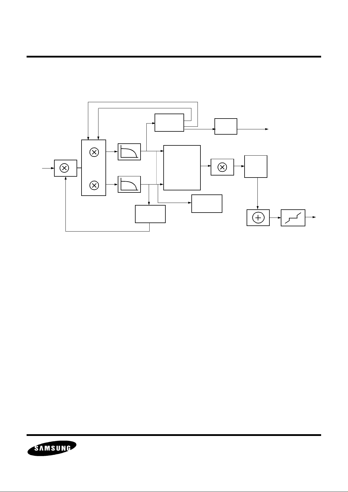
1.4. HORIZONTAL CHROMA PROCESSING
A simplified block diagram for the horizontal chroma processing unit is shown in Figure 17.
FROM ADC
Saturation
Control
COS
SIN
Low
Pass
CBW,FSEC
Low
Pass
CBW,FSEC
Tracking
V
U
Gain
Frequency
Tracking
CFTC
HUE, TSTCFR
SECAM
Frequency
Differentiator
SAT
CGTC
CKILL
TSTCGN
Auto
Detect
RTCO
Control
RTC_DTO
RTC_PID
Gain / PAL
Control
UGAIN
VGAIN
Figure 17. Horizontal Chroma Processing Unit
CKILL
Offset
Control
UOFFST
VOFFST
Color
Killer
Coring
Control
CORE
The KS0127B supports chroma input in NTSC, PAL, SECAM and component formats. The color standard is
automatically detected and the various chroma processing blocks are enabled as required for the given chroma
standard. Details of the various chroma processing blocks follow.
1.4.1. IF Compensation
For improved chroma demodulation when the input video is from a mis-tuned IF source, an IF compensation filter
is included that has variable gain for the upper chroma side band. This is controlled by the CIFCMP[1:0] bits at
location CDEM. The frequency response is shown in Figure 18. For convenience, all plots are normalized to the
NTSC modulation frequency.
Modified on May/04/2000
PAGE 23 OF 96
ELECTRONICS

KS0127B Data Sheet MULTIMEDIA VIDEO
Figure 18. Chroma IF Compensation Frequency Response
1.4.2. Demodulation Gain
The demodulation gain block is controlled by feedback from the gain tracking block. For NTSC and PAL type
inputs, the gain constant is derived from a programmable reference compared against the U component of the
input video. This reference is controlled by the SAT register. The default value “0” is the correct gain (saturation for
nominal output). For SECAM type input, the feedback is calculated such that proper frequency demodulation is
obtained. When external calibration is desired, the gain feed back loop can be “opened” by setting TSTCGN=1.
The SAT then controls bits 8 through 1 of a 10 bit multiplier.
For standard auto tracking applications, it is recommended that the SAT register be used as an end user saturation
control. This register is 2’s compliment.
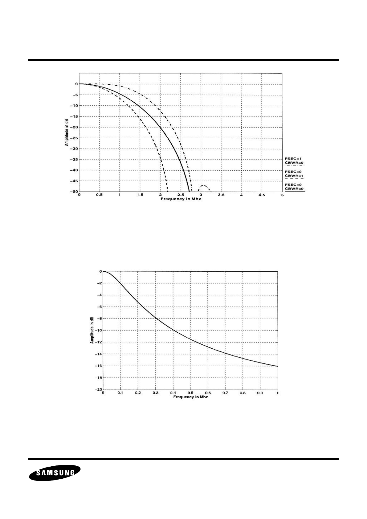
1.4.3. Demodulation Low Pass Filter
The demodulation circuit also contains a programmable low pass filter and a coring function for noise reduction.
The chroma low pass filter frequency response for the demodulation circuit for the various video standards are
shown in Figure 19
ELECTRONICS
Modified on May/04/2000
PAGE 24 OF 96
KS0127B Data Sheet MULTIMEDIA VIDEO
Figure 19. Chroma Low Pass Filter Frequency Response
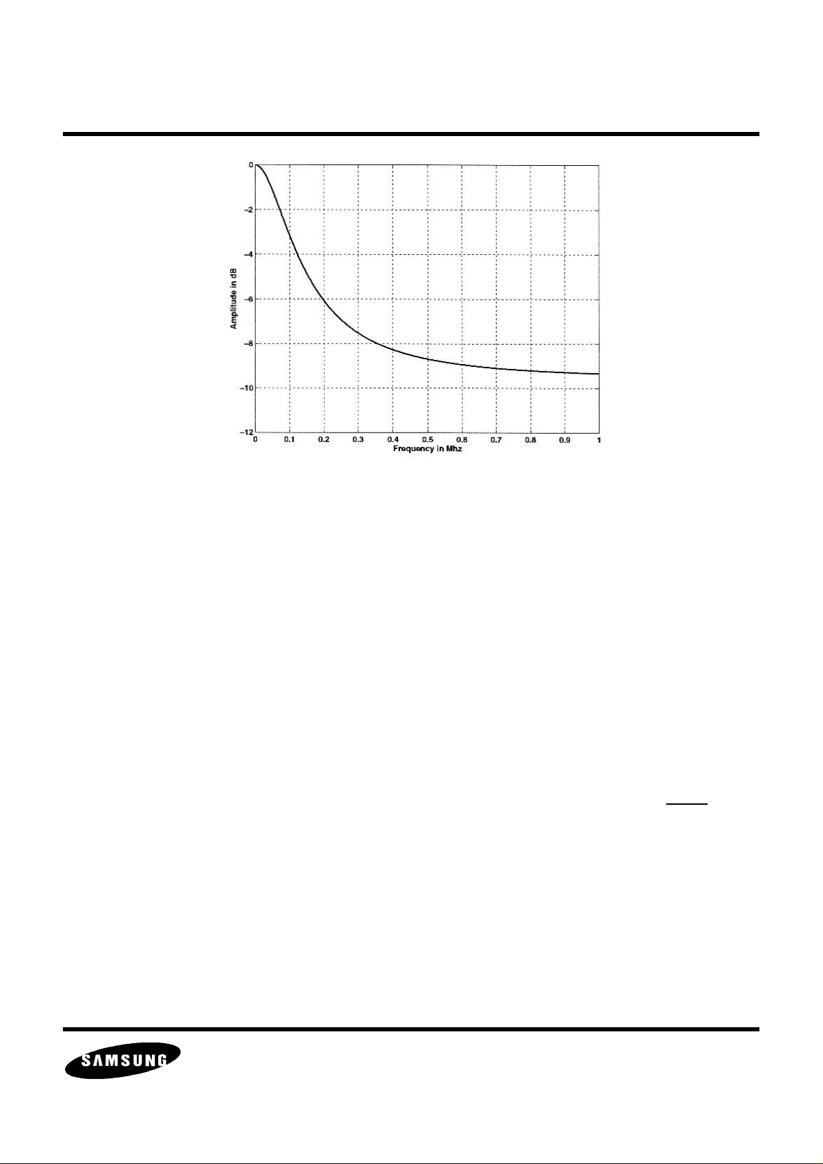
1.4.4. SECAM Demodulation
SECAM processing includes a frequency differentiator, a Cloche and a de-emphasis filter. Frequency response for
the filters are shown in Figure 20 and Figure 21.
Figure 20. Cloche Filter Frequency Characteristic
ELECTRONICS
Modified on May/04/2000
PAGE 25 OF 96
KS0127B Data Sheet MULTIMEDIA VIDEO
Figure 21. De-emphasis Filter Frequency Response
1.4.5. Additional Chroma Functions
KS0127B has many built in auto detection circuits. These allow KS0127B to track any type of video standard input
automatically.
For analog component video input, the demodulation function is not enabled. The low pass filter provides a group
delay for Cb and Cr alignment. This enables the two components to be sampled by one ADC.
An RTCO serial output is provided that encodes the current chroma and pixel frequency of the decoder. This
information can be used by an Encoder running off of the decoder clock to produce proper color output. The
horizontal position of the serial signal is controlled by the HS2 location. The phasing of the DTO and the Encoder
can be reset using the RTC_DTO bit. For PAL mode, the PID polarity can be controlled with the RTC_PID bit.
1.5. COMB FILTER
Comb filters provide superior Y/C separation for composite NTSC and PAL than simple chroma trap filter. The
KS0127B contains on-chip separate 2-line stored luma and chroma comb filters. An internal signal COMB controls
for what lines the comb function is enabled. This signal is available through the PORTB pin. Combing is part of the
vertical processing which also includes vertical scaling, which is discussed in Section 1.6. A block diagram for the
vertical processing section is shown in Figure 22.
ELECTRONICS
Modified on May/04/2000
PAGE 26 OF 96

KS0127B Data Sheet MULTIMEDIA VIDEO
Luma
Vertical
Scaler
Luma
Adaptive
Comb
Chroma
Vertical
Scaler
Chroma
Comb
Luma
Chroma
Horizontal
Scaler
Horizontal
Scaler
Figure 22. Vertical Processing
1.5.1. Luma Comb Filter
The luma comb filter reduces high frequency chroma leakage into the luminance path. The KS0127B uses 2-line
stored luma data for combing. Filter coefficients for different video input standards are provided and can be
selected automatically based on the video input. Filter coefficients may also be set manually.
Vertical
BW
Retention
Sum
Y
C
An optional active comb is employed for NTSC video. Selection of luma comb coefficients is based on line-to-line
chroma correlation.
Provision is made to disable luma comb for S-video, component, or digital video input. This is achieved by
programming the luma comb control register MNYCMB to “1”, and by choosing the value 3 or 4 for YCMBCO[2:0].
This will result either a 1-line or 2-line luma delay. Care must be exercised when disabling the luma comb so that
luma line delay matches the chroma path line delay.
Special filtering is applied to ensure that high vertical bandwidth is retained for the luma path.
1.5.2. Chroma Comb Filter
The chroma comb filter provides further color separation from the composite video. Filter coefficients can be
automatically selected based on the input video standard or manually set using NMCCMB and CCMBCO[2:0].
ELECTRONICS
Modified on May/04/2000
PAGE 27 OF 96

KS0127B Data Sheet MULTIMEDIA VIDEO
1.6. SCALING
The KS0127B includes a high quality down scaler. The video images can be down scaled in both horizontal and
vertical direction to an arbitrary size.
1.6.1. Horizontal Scaler
The horizontal scaler uses a 5-tap 32-phase interpolation filter for luma, and a 3-tap 8-phase interpolation filter for
chroma. Scaled pixel data are stored in an on-chip FIFO so they can be sent out in a continuous stream.
Horizontal scaling ratio is programmed via the 15-bit register HSCL. The timing signal EHAV is used to indicate
when scaled pixel data is available at the video output port. EHAV can be programmed so that it is active for every
line regardless of vertical cropping and scaling. Or it can be programmed to be active only for valid video lines. For
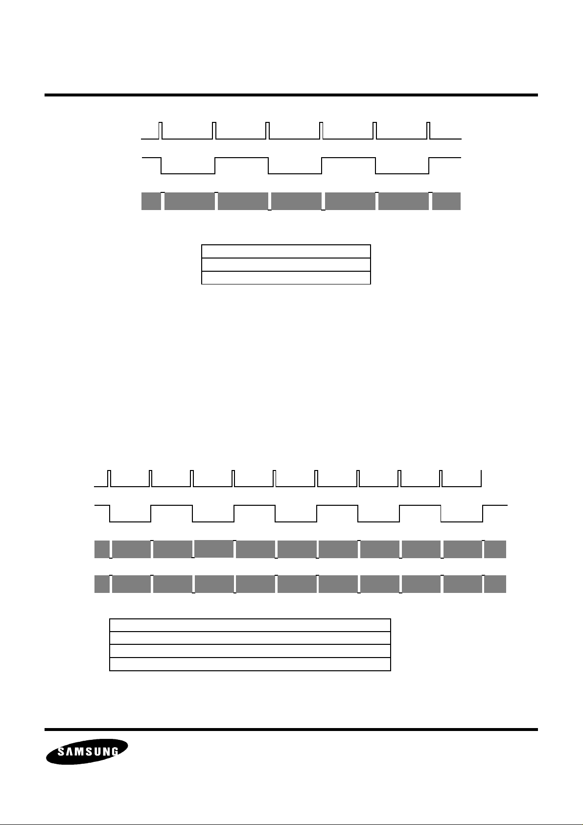
example, Figure 23 shows the timing for CIF output assuming HAV is programmed to be active for 720 pixels. The
HSCL register is programmed with the value 4000 (hex). The trailing edge of EHAV is either aligned with the
trailing edge of HAV if the total number of scaled pixels is even, or is one pixel clock earlier if the number is odd.
CK2
HAV
EHAV
Y[7:0]
C[7:0]
720
360
-
Y
Y
0
U
0
Y2Y
1
U2V
V
0
-
3
- -
2
Y
356
U
356
Y
357Y358Y359
V
356U358V358
Figure 23. Horizontal Scaler Timing for CIF Output (CCIR 601 Pixel Rate)
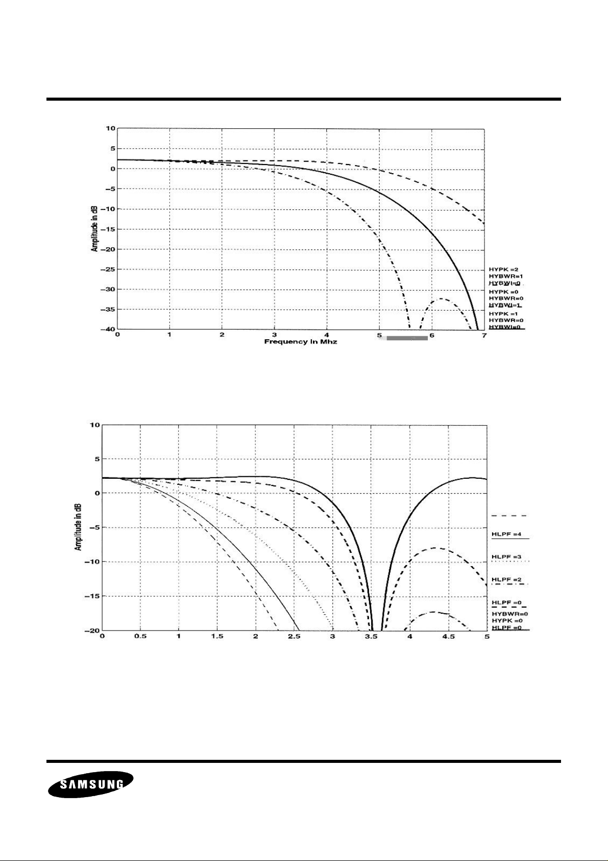
Frequency response and group delay for the luma scaler are shown in Figure 24 and Figure 25, respectively. The
luma interpolation filter is designed to achieve relatively flat frequency response and minimal group delay up to the
normal video bandwidth. A flat full data path frequency response may be obtained with the help of the luma
peaking control register HYPK[1:0]. The high quality filter ensures minimal artifacts for any scaling ratio.
ELECTRONICS
Modified on May/04/2000
PAGE 28 OF 96

KS0127B Data Sheet MULTIMEDIA VIDEO
Figure 24. Horizontal Luma Scaler Interpolation Filter Frequency Response
3
2.5
2
group delay (13.5MHz Clocks)
1.5
1
Figure 25. Horizontal Luma Scaler Interpolation Filter Group Delay
Because of the limited bandwidth of the chroma data, a simpler interpolation filter is used for the horizontal chroma
scaler. The frequency response and group delay for this filter are shown in Figure 26 and Figure 27, respectively.
ELECTRONICS
Modified on May/04/2000
PAGE 29 OF 96
 Loading...