

Samsung KS0123 Datasheet

KS0123 Data Sheet
S
P
DIGITAL VIDEO ENCODER
MULTIMEDIA VIDEO
The KS0123 multi-standard video encoder converts CCIR
656 8-bit multiplexed digital component video into analog
baseband signals. It outputs composite video (CVBS) and
S-Video simultaneously at three analog output pins.
The encoder implements Macrovision revision 6.0 antitaping scheme. Additionally, it contains a color subcarrier
genlock to support analog/digital video splicing.
The video outputs conform to either SMPTE 170M (NTSC)
or CCIR 624 (PAL) standards.
FEATURES
• Macrovision revision 6.0 anti-taping support
• 8-bit parallel CCIR 656 CbYCr input format
• Synchronizes to CCIR 656 AVE time reference codes
for horizontal and vertical timing generation in slave
mode operation
• Generates HSYN and FIELD signals in master mode
operation
• Programmable subcarrier frequency, SCH phase,
and synchronous field display to support MPEG II
picture-coding-extension
• Optional subcarrier genlock to analog f
ence
• 650 kHz or 1.3 MHz chrominance bandwidth selection
• Support NTSC, PAL, PAL-M and PAL-N
• Switchable pedestal with gain compensation
• Selectable 37 nsec YC delay pre-compensation
• Video outputs meet SMPTE 170M or CCIR 624 spec
sc_ref
refer-
44 PLCC
ORDERING INFORMATION
Device Package Temperature Range
KS0123 44 PLCC 0°~+70°C
• 27 MHz DAC conversion rate
• Triple 10-bit DAC’s for simultaneous S-video
and composite output
• 2 -wire serial host interface
• 8 general purpose I/O pins
• JTAG test interface
• Single 5 V supply with power down mode
• 44-pin PLCC package
Application
• Settop Box Video Encoding
• MPEG Playback
• Multimedia
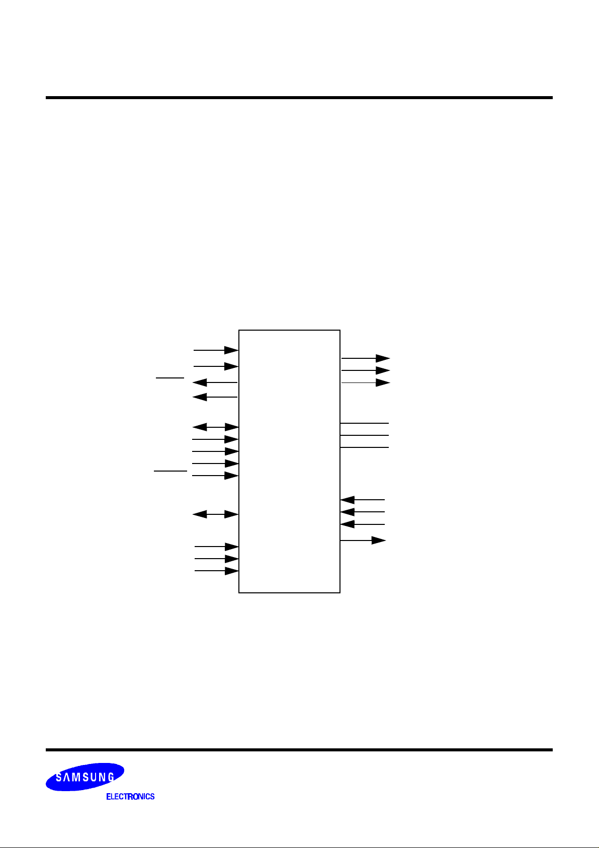
BLOCK DIAGRAM
PXCK
Demux
PD[7:0]
HSYN
FIELD
SDA
SCL
SA1
SA2
RESET
General purpose
and
Sync
extract
Host Interface
I/O
Interpolator
4:2:2/4:4:4
Video
Timing
Gen
JTAG
TDI
TMS
TCK
TDO
Y
B-Y
R-Y
LPF
LPF
Sync
& Blank
insert
Subcarrier
Synthesizer
Genlock
Interface
Chroma
Modulator
Genlock
INT
C_FSCSC_REF
ALID
+
10-bit
DAC
10-bit
DAC
10-bit
DAC
D/A
Ref.
C
Y
CVBS
Analog
Interface
CSync
Clamp
PAGE 1 OF 44Modified on May/04/2000

KS0123 Data Sheet
PIN ASSIGNMENT - 44 PLCC
PD5
40
PD4
41
PD3
42
PD2
43
PD1
44
VDD
1
VSS
2
PD0
3
SA2
4
SA1
5
PD6
PD7
VDD
VSS
C
VDDA
BYPASS
39 38 37 36 35 34 33 32 31 30 29
VSSA
Y
CVBS
KS0123
MULTIMEDIA VIDEO
VSSA
RREF
28
VREF
27
VDDA
26
PXCK
25
VSS
24
VDD
23
RESET
22
TCK
21
TMS
20
TDI
19
SDA
6
7
8 9 10 11 12 13 14 15 16 17
SCL
SC_REF
D7/PAL_ID
D6/SC_SYNC
D5
TYPICAL APPLICATION
The Encoder is shown in a typical settop box application.
CHANNEL
DECODER
MPEG
VIDEO
DECODER
TDO
18
D4
D3/HSYN
VSS
D2/FIELD
ENCODER
KS0123
D1/CLAMP
D0/CSYN
TV Monitor
Figure 1. Typical Application
Modified on May/04/2000
PAGE 2 OF 44
KS0123 Data Sheet
MULTIMEDIA VIDEO
PIN DESCRIPTION
Pin Name Pin # Type Description
CLOCK INPUT
PXCK 25 I 27 MHz clock input. TTL/CMOS.
PIXEL DATA PORT
PD7 - PD0 38-44, 3 I Pixel data inputs. TTL/CMOS.
GENERAL PURPOSE PORT AND OTHER SIGNALS
SC_REF 8 I Subcarrier reference input. TTL.
D7/PAL_ID 9 I/O General Purpose I/O Port 7 or PAL_ID input. TTL/CMOS.
D6/SC_SYNC 10 I/O General Purpose I/O Port 6 or SC_SYNC input. TTL/CMOS.
D5 11 I/O General Purpose I/O Port 5. TTL/CMOS.
D4 12 I/O General Purpose I/O Port 4. TTL/CMOS.
D3/HSYN 14 I/O General Purpose I/O Port 3 or HSYN output. TTL/CMOS.
D2/FIELD 15 I/O General Purpose I/O Port 2 or FIELD output. TTL/CMOS.
D1/CLAMP 16 I/O General Purpose I/O Port 1 or CLAMP output. TTL/CMOS.
D0/CSYN 17 I/O General Purpose I/O Port 0 or CSYN output. TTL/CMOS.
SERIAL MICROPROCESSOR PORT
SDA 6 I/O Serial data I/O. Open drain.
SCL 7 I Serial clock input.
SA1 5 I Slave address select. TTL.
SA2 4 I Slave address select. TTL.
RESET
RESET 22 I Master reset input. TTL.
VIDEO OUTPUTS
CVBS 30 O Composite video output.
Y 32 O Luminance output.
C 35 O Chrominance output.
DAC REFERENCE AND COMPENSATION
VREF 27 I/O Voltage reference I/O. Connect a 0.1 µF capacitor to VSSA.
BYPASS 33 I/O Compensation capacitor. Connect a 0.1 µF capacitor to VDDA.
RREF 28 I/O Current setting resistor.
Modified on May/04/2000
PAGE 3 OF 44
KS0123 Data Sheet
PIN DESCRIPTION (Continued)
Pin Name Pin # Type Description
JTAG PORT
TDI 19 I Data input port. TTL.
TMS 20 I Scan select input. TTL.
TCK 21 I Scan clock input. TTL.
TDO 18 O Data output port. CMOS.
POWER
VDD 1,23,37 +5V Digital power supply.
VDDA 26,34 +5V Analog power supply.
GROUND
VSS 2,13,24,36 0V Digital ground.
VSSA 29,31 0V Analog ground.
MULTIMEDIA VIDEO
Modified on May/04/2000
PAGE 4 OF 44
KS0123 Data Sheet
MULTIMEDIA VIDEO
PIN CROSS REFERENCE
Numerical Order by Pin Number
Pin # Name Pin # Name Pin # Name Pin # Name
1 VDD 12 D4 23 VDD 34 VDDA
2 VSS 13 VSS 24 VSS 35 C
3 PD0 14 D3/HSYN 25 PXCK 36 VSS
4 SA2 15 D2/FIELD 26 VDDA 37 VDD
5 SA1 16 D1 27 VREF 38 PD7
6 SDA 17 D0 28 RREF 39 PD6
7 SCL 18 TD0 29 VSSA 40 PD5
8 SC_REF 19 TD1 30 CVBS 41 PD4
9 D7/PAL_ID 20 TMS 31 VSSA 42 PD3
10 D6/SC_SYNC 21 TCK 32 Y 43 PD2
11 D5 22 RESET 33 BYPASS 44 PD1
Alphabetical Order by Pin Name
Name Pin # Name Pin # Name Pin # Name Pin #
BYPASS 33 PD0 3 SA1 5 VDD 37
C 35 PD1 44 SA2 6 VDDA 26
CVBS 30 PD2 43 SCL 7 VDDA 34
D0 17 PD3 42 SC_REF 8 VREF 27
D1 16 PD4 41 SDA 6 VSS 2
D2/FIELD 15 PD5 40 TCK 21 VSS 13
D3/HSYN 14 PD6 39 TDI 19 VSS 24
D4 12 PD7 38 TDO 18 VSS 36
D5 11 PXCK 25 TMS 20 VSSA 29
D6/SC_SYNC 10 RESET 22 VDD 1 VSSA 31
D7/PAL_ID 9 RREF 28 VDD 23 Y 32
Modified on May/04/2000
PAGE 5 OF 44
KS0123 Data Sheet
MULTIMEDIA VIDEO
GENERAL DESCRIPTION
The encoder accepts 27 MHz 8-bit multiplexed digital component video in CCIR 656 CbYCr format at the Pixel
Data (PD) port. The pixel data are demultiplexed into luminance and chrominance components for interpolation
and low pass filtering to reduce cross luma/chroma interference. The filtered chrominance signals are modulated
onto a color subcarrier and added to the processed luminance components to form the composite video (CVBS).
The digital CVBS and S-Video signals are interpolated to 27 MHz rate and then converted to analog forms by 3 10bit D/A converters.
Anti-taping pulses, synch signals and color burst are generated internally. The rise and fall times of those pulses
are controlled to reduce ringing. The shaped signals are inserted into the video stream controlled by the timing
generator.
The encoder also contains a color subcarrier PLL, which when enabled will frequency and phase lock the color
subcarrier to an external analog fsc or 4 x fsc reference. The SCH phase can be adjusted to compensate for
additional external phase delay.
VIDEO DATA INPUT
PD[7:0]
PXCK
HSYN
FIELD
SDA
HOST
INTERFACE
GENERAL PURPOSE
PORT
GENLOCK
INPUT
SCL
SA1
SA2
RESET
D[7:0]
SC_REF
SC_SYNC
PAL_ID
DIGITAL
VIDEO
ENCODER
VIDEO OUTPUTS
CVBS
Y
C
ANALOG INTERFACE
VREF
BYPASS
RREF
JTAG TEST INTERFACE
TDI
TMS
TCK
TDO
Figure 2. Logic Diagram
Modified on May/04/2000
PAGE 6 OF 44

KS0123 Data Sheet
MULTIMEDIA VIDEO
DIGITAL VIDEO INPUT FORMAT
Video data enters the encoder on pins PD[7:0]. The encoder accepts and processes digital video data in
accordance with CCIR 656 and CCIR 601 standards. The input data are 8 bit multiplexed CbYCr component video,
encoded in the 4:2:2 format. The input bit stream may contain End of Active Video (EAV) and Horizontal Ancillary
Control (HANC) codes. The relationships of the digital video with analog timing are show in Figure 3.
CCIR 656 Timing Relationship Between Video Data and The Analog Sync Waveform
The digital active line begins at 244 words (in the 525-line standard) or at 264 words (in the 625-line standard) after
the leading edge of the analog line synchronization pulse, this time being specified between half-amplitude points.
Analog line blanking
16T (625)
8T (525)
4T
O
H
24T (625)
32T (525)
E
HANC
A
V
Digital line blanking
288T (625)
276T (525)
T: clock period 37ns nom.
SAV: start of active video timing ref. code
EAV: end of active video timing ref. code
HANC: horizontal ancillary data
Figure 3. 656 Data Format and Timing Relationship
S
A
V
Digital line
1728T (625)
1716T (525)
TV line 64us (625)
63.5us (525)
20T (625)
10T (525)
Video data block
1448T
Multiplexed video data
CB Y CR Y CB Y...
4T
Digital active line
1440T
E
A
V
O
H
HANC
Modified on May/04/2000
PAGE 7 OF 44

KS0123 Data Sheet
MULTIMEDIA VIDEO
Timing Reference Codes
Each video line can have two timing reference codes, one at the beginning of the data block (start of active video
SAV) and one at the end (end of active video EAV) as shown in Figure 3. Each timing reference code consists of a
four byte sequence in the form FF, 00, 00 and XX as shown in Table 1. The first three words are fixed, the fourth
byte contains field and line blanking information.
Table 1: Video Timing Reference Codes
Bit # 7(MSB) 6 5 4 3 2 1 0(LSB) HEX
First 1 1 1 1 1 1 1 1 FF
Second 0 0 0 0 0 0 0 0 00
Third 0 0 0 0 0 0 0 0 00
Fourth 1 F V H P
Notes: F =
0 during field 1
P
3
P
2
P
1
0
XX
1 during field 2
V =
0 elsewhere
1 during field blanking
H =
0 in SAV
1 in EAV
P3 - -
P0: Protection bits (not used by the encoder)
The encoder decodes the video timing reference code that indicates the end of active video (EAV). The EAV code
shall contain the F (field) and V (blanking) bits as specified in CCIR 656. This information applies to the following
video line. The encoder ignores the start of active video (SAV) timing code.
The encoder uses the F bit for synchronization purposes. The transition of F bit is used to indicate the start of a
new field. The polarity is also used to indicate odd and even. Additional field information is supplied by the ancillary
data.
The V bit is not used for synchronization. A V of ‘1’ indicates line blanking. Certain lines and half lines are blanked
regardless of the state of the V bit. In general if the V bit is high, then the encoder blanks the line (Figure 10 and
Figure 11).
Modified on May/04/2000
PAGE 8 OF 44

KS0123 Data Sheet
MULTIMEDIA VIDEO
Horizontal Ancillary Data Sequence (HANC)
The ancillary data contains additional timing information about the following video line. Table 2 shows the
sequence of the ancillary data. The HANC data, if present, should immediately follow the EAV code. The encoder
decodes the ancillary data if the ancillary data type code (TT) matches the data ID code stored in the internal
ANCDID register (index 07h).
The LSB of the ancillary data is a parity bit. The video encoder assumes that the data is error free and always
ignores this bit.
Table 2: Ancillary Data Sequence
Word ID Description B7 B6 B5 B4 B3 B2 B1 B0
ANC(2) Ancillary Data
ANC(1) 1 1 1 1 1 1 1 1
ANC(0) 1 1 1 1 1 1 1 1
TT Data Type TT6 TT5 TT4 TT3 TT2 TT1 TT0 P
FIELD Field number and
PH(1) Subcarrier
PH(0) PH6 PH5 PH4 PH3 PH2 PH1 PH0 P
FR(4) Subcarrier
FR(3) FR27 FR26 FR25 FR24 FR23 FR22 FR21 P
FR(2) FR20 FR19 FR18 FR17 FR16 FR15 FR14 P
FR(1) FR13 FR12 FR11 FR10 FR9 FR8 FR7 P
FR(0) FR6 FR5 FR4 FR3 FR2 FR1 FR0 P
Header
Reserved (R) (R) (R) (R) (R) (R) (R) P
synchronous
video flag
Instantaneous
Phase
Frequency
0 0 0 0 0 0 0 0
(R) (R) (R) (R) (R) (R) (R) P
(R) (R) (R) SVF/ F2 F1 F0 P
PHV PH12 PH11 PH10 PH9 PH8 PH7 P
FRV (R) (R) FR31 FR30 FR29 FR28 P
Note: 1. P = odd parity bit
2. R = reserved bit; ignored by video encoder
The ancillary data header (ANC) consists of three bytes which indicate the start of the ancillary data. This is in
accordance with CCIR 656.
The data type code is used to specify the ancillary data type. The encoder compares this value with the value
programmed into the ANCDID register. If the two match, the encoder will process the ancillary data, otherwise the
encoder will ignore the ancillary data.
The field number bits are used by the encoder to program the field counter. The field number will be loaded to the
counter if SVF/ is low and the ancillary timing reference enable (ATMEN) bit is ‘1’.
Modified on May/04/2000
PAGE 9 OF 44
KS0123 Data Sheet
The subcarrier instantaneous phase is a 13-bit integer which defines the phase of the reference subcarrier at the
synch tip. The subcarrier frequency synthesizer phase will be reset to this number at the synch tip when both
HANC datum PHV and control register APHEN are ‘1’s.
Table 3: Definition of Subcarrier Instantaneous Phase
subcarrier phase # phase value
0 ([3600 / 8192]) * 0
1 ([3600 / 8192]) * 1
... ...
8191 ([3600 / 8192]) * 8191
The MPEG II system allows the 27 MHz clock frequency to vary to prevent the input buffer from overflow or
underflow. When this happens the color subcarrier frequency will shift if the addend of numerical oscillator is not
adjusted accordingly. If control register bit AFREN is ‘1’ the subcarrier synthersizer will select the latched HANC’s
subcarrier frequency data (FR) as the addend instead of the programmable register (0x8-0xb) (Figure 6). The FR
is latched if HANC datum FRV = ‘1’. and the HANC control register’s AFREN bit is set. The FR’s value should be
calculated using the equation
Fsc
32
FRNINT 2
=
----------
•
Ck
MULTIMEDIA VIDEO
where Fsc is the desired color subcarrier frequency,
Ck is the clock frequency,
and NINT is the nearest integer.
Modified on May/04/2000
PAGE 10 OF 44
KS0123 Data Sheet
024681012
-45
-40
-35
-30
-25
-20
-15
-10-50
Mhz
d
b
0123456-2-1.8
-1.6
-1.4
-1.2-1-0.8
-0.6
-0.4
-0.20Mhz
d
b
MULTIMEDIA VIDEO
VIDEO ENCODING
The incoming digital video are gain and offset adjusted according to the output format, NTSC or PAL, controlled by
the format register. Both the luminance and chrominance are band limited and interpolated to 27 MHz sampling
rate for digital to analog conversion. The NTSC output can be selected to include a 7.5 IRE pedestal. The user can
also select either 650 kHz or 1.35 MHz chrominance bandwidth. The U and V components have equal
bandwidth.
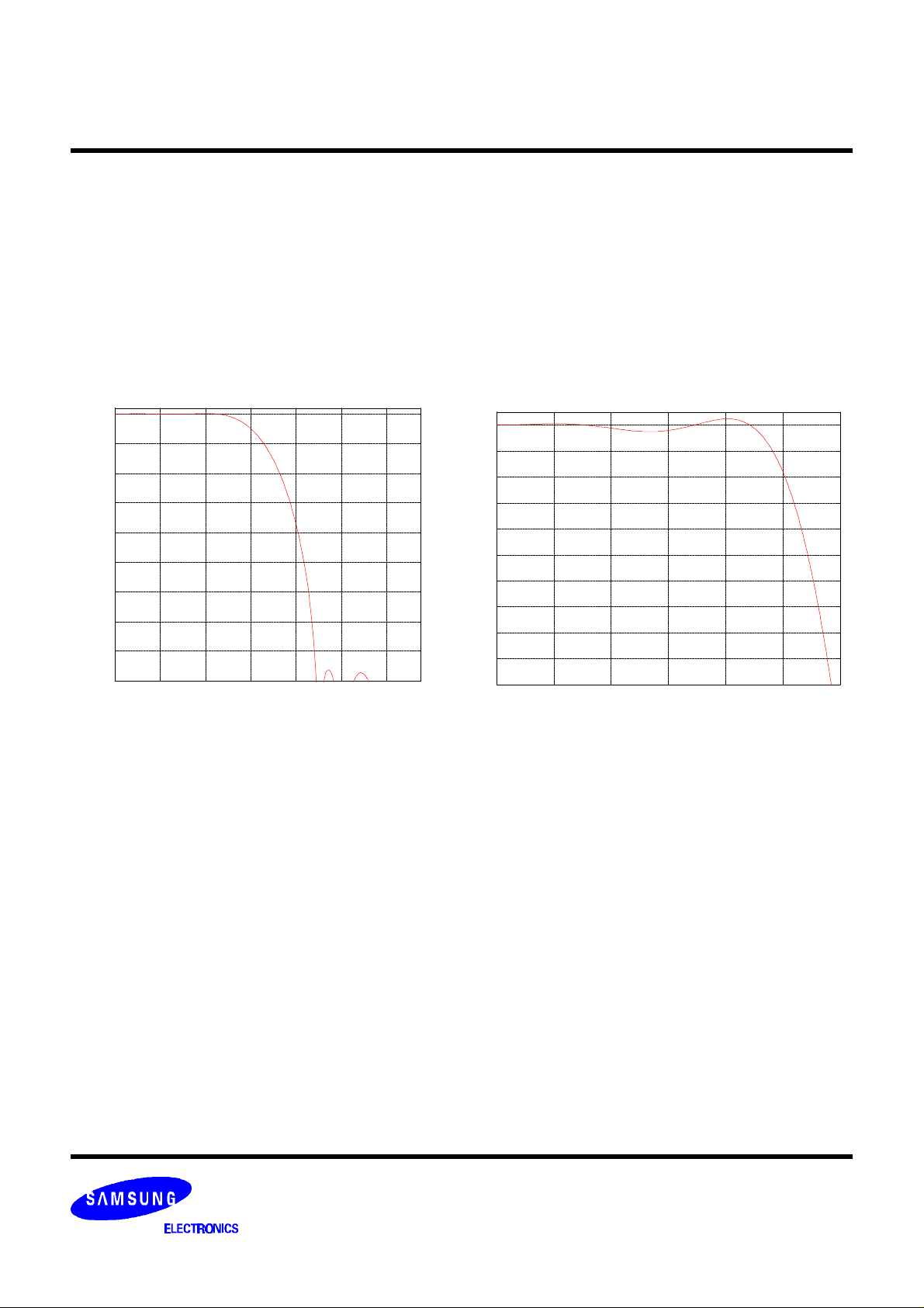
Luminance Filter
The luminance signal is band-limited to 6 MHz. The filter is implemented with a 15 tap linear phase FIR filter. Figure
4 shows the frequency responses.
Figure 4. Luminance Filter Frequency Response
Modified on May/04/2000
PAGE 11 OF 44
KS0123 Data Sheet
0
0.511.522.5
-25
-20
-15
-10-50
Mhz
d
b
0
0.511.522.533.544.55-25
-20
-15
-10-50
Mhz
d
b
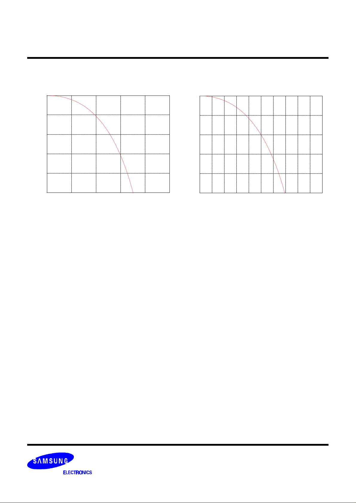
Chrominance Filter
Figure 6 shows the chrominance frequency response for different bandwidth selections.
MULTIMEDIA VIDEO
CHRBW = ‘0’
Figure 5. Chrominance Filter Frequency Response
CHRBW = ‘1’
Modified on May/04/2000
PAGE 12 OF 44
KS0123 Data Sheet
MULTIMEDIA VIDEO
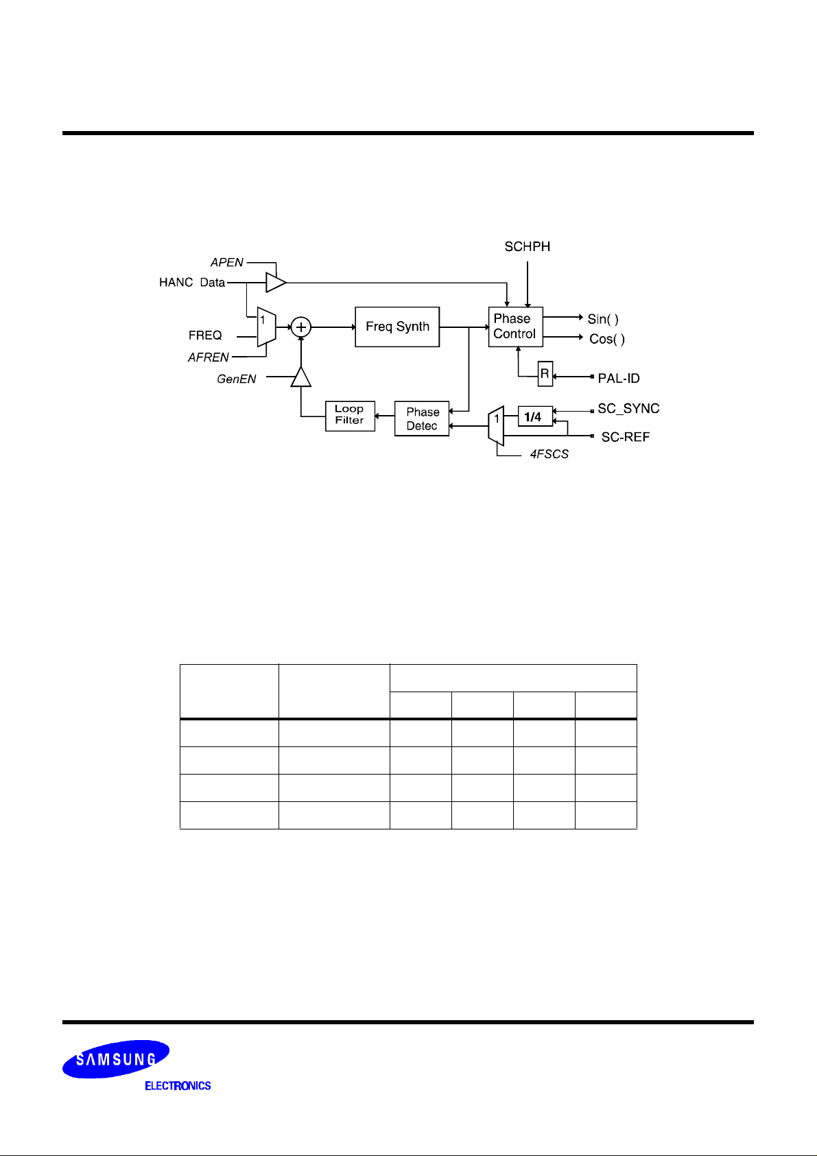
COLOR SUBCARRIER GENERATION
The chrominance signals are modulated onto a subcarrier. The nominal subcarrier frequency is determined by 4
registers (08h - 0Bh). The subcarrier generation also contains Subcarrier Horizontal Synch Phase, SCH, offset
control (Reg 0Ch - 0Dh), and genlock functions to support digital/analog video multiplexing.
PH
FR
Figure 6. Fsc Synthersizer
The color subcarrier synthesizer can operate in 3 modes: (a) free running mode, (b) HANC genlock mode, and (c)
analog genlock mode.
(a). In the free running mode the color subcarrier frequency is programmed via the host interface. The 4 field or 8
field SCH phase are maintained. The nominal frequency register values for different video standards are listed in
Table 4.
Table 4: Register Values for Subcarrier Frequencies
Standard
NTSC 3.57954545 43 E0 F8 3E
PAL-B,G,H,I 4.43361875 54 13 15 96
PAL-M 3.57561189 43 CD DF C7
PAL-N 3.58205625 43 ED 28 8D
(b). In the HANC genlock mode the subcarrier frequency, FR, and instantaneous phase, PH, information are sent
to the encoder via the HANC data. The frequency and phase values are updated during the synch tip.
(c). If analog genlock mode is selected the subcarrier synthesizer is locked to an external reference signal, fsc or
4 fsc. An external PAL_ID signal is required to control the PAL phase alternation. The PLL has 2 kHz pull in range.
Subcarrier
Frequency(MHz)
FREQD FREQC FREQB FREQA
Frequency Register
Analog Genlock Circuit
The analog genlock circuit will lock the frequency and phase of the subcarrier synthesizer to an external reference
signal. To activate the genlock circuit, first program the nominal FREQD-A value then set GENEN = 1.The external
Modified on May/04/2000
PAGE 13 OF 44
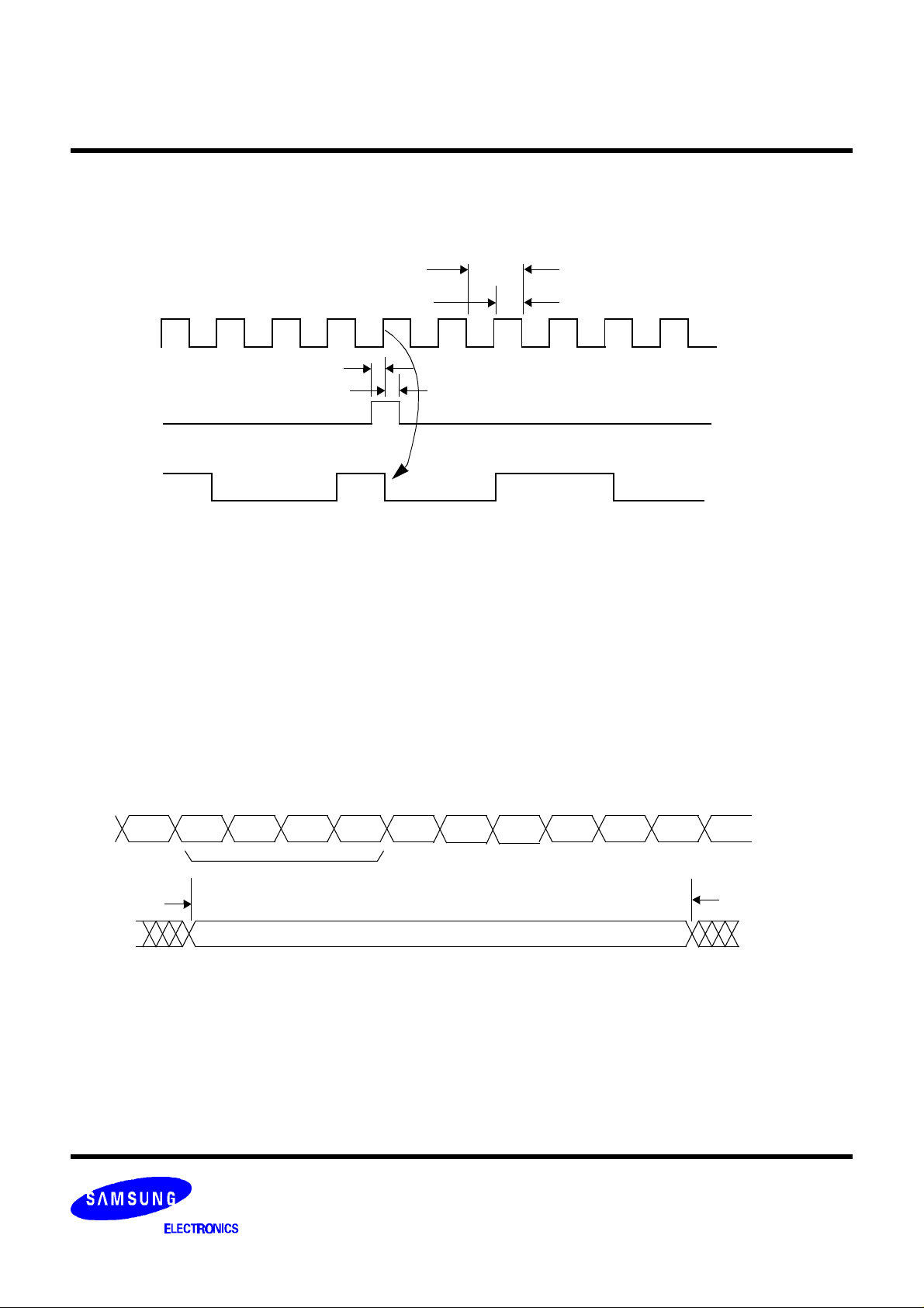
KS0123 Data Sheet
reference signal is applied to the SC_REF input pin. The frequency of this squarewave is either Fsc or 4*Fsc
(program the 4FSCS bit accordingly). When using a 4*Fsc input, the SC_SYNC resets the internal divider’s phase
to the 0 count state as shown in Figure 7. The SCHM and SCHL registers can be programmed to compensate for
the propagation delay from the phase detector input to the DAC output.
1/(4 *SC_REF)
SC_REF(== 4fsc)
t
SU;SC_SYNC
t
HD;SC_SYNC
t
PWH;SC_REF
MULTIMEDIA VIDEO
SC_SYNC
internal divided by 4 counter output
Figure 7. SC_REF and SC_SYNC Input Timing
PAL_ID Input
The PAL_ID input is used by the analog genlock circuit to control the PAL chroma V-axis inversion. PAL_ID is only
recognized when GENEN = 1 and the video format is PAL. PAL_ID is low for lines where the color burst phase is
135ο, and high for lines where the color burst phase is -135o. PAL_ID is sampled and its value is used on the
following line. The PAL_ID should be valid during the time interval corresponding to video samples 1440 to 1449.
See Figure 8 for the PAL_ID timing requirement.
Pixel Data Input (PD[7:0])
1439 1440 1441
Y 719
$FF
$00 $00 $XX
EAV Sequence
D7 Input (PAL_ID)
Ancillary Data...
t
DUR;PAL_ID
PAL_ID Stable
Figure 8. PAL_ID Input Timing
Sample number
1448144714461445144414431442 1449
1450
Modified on May/04/2000
PAGE 14 OF 44
 Loading...