

Samsung KS0108B Datasheet

KS0108B 64 CH SEGMENT DRIVER FOR DOT MATRIX LCD
INTRODUCTION
The KS0108B is a LCD driver LSl with 64 channel output
for dot matrix liquid crystal graphic display system. This
device consists of the display RAM, 64 bit data latch 64 bit
drivers and decoder logics. It has the internal display RAM
for storing the display data transferred from a 8 bit micro
controller and generates the dot matrix Iiquid crystal driving signals corresponding to stored data.The KS0108B
composed of the liquid crystal display system in combination with the KS0107B (64 common driver)
FEATURES
• Dot matrix LCD segment driver with 64 channel output
• Input and Output signal
- Input: 8 bit parallel display data
Control signal from MPU
Splitted bias voltage (V1R, V1L, V2R, V2L,
V3R. V3L, V4R, V4L)
- Output: 64 channel waveform for LCD driving.
• Display data is stored in display data RAM from MPU.
• Interface RAM
- Capacity: 512 bytes (4096 bits)
- RAM bit data: RAM bit data = 1:ON
RAM bit data- = 0:OFF
• Applicable LCD duty: 1/32~1/64
• LCD driving voltage: 8V~17V(VDD-VEE)
• Power supply voltage: + 5V±10%
COMMON SEGMENT
KS0107B Other KS0108B MPU
• High voltage CMOS process.
• 100QFP and bare chip available.
Driver Controller
100 QFP

KS0108B 64 CH SEGMENT DRIVER FOR DOT MATRIX LCD
BLOCK DIAGRAM
CLK2CLK1DB<0:7>
CS1B
CS2B
CS3
R/W
RS
E
RSTB
DISPLAY
ON/OFF
INPUT REGISTER
1
OUTPUT REGISTER
8
BUSY
8
INSTRUCTION
DECODER
I/O
BUFFER
FRM
V0L
V2L
V3L
V5L
6
Y-COUNTER
6
6
DISPLAY START LINE REGISTER
CL
M
S64 S63 S2 S1
6
Z DECODER
64
Y-DECODER
64
DISPLAY DATA RAM
512¡¿8=4096 bits
64
DATA LATCH
64
LCD DRIVER
3
X-DECODER
8
8
PAGE SELECTOR
ADC
V0R
V2R
V3R
V5R

KS0108B 64 CH SEGMENT DRIVER FOR DOT MATRIX LCD
CS2B
CS1B
RSTB
R/W
RS
95
94
93
CS3
92
91
90
NC
NC
NC
89
88
87
86
DB7
DB6
85
DB5
84
KS0108B
36
37
38
39
40
41
42
43
44
45
46
47
S26
S27
S28
S29
S30
S31
S32
S33
S34
S35
S36
S37
DB4
83
48
S25
DB3
82
49
S24
DB2
81
50
S23
80 79 78 77 76 75 74 73 72 71 70 69 68 67 66 65 64 63 62 61 60 59 58 57 56 55 54 53 52 51
DB1
DB0
V
SS
V3L
V2L
V5L
V0L
V
EE1
S1
S2
S3
S4
S5
S6
S7
S8
S9
S10
S11
S12
S13
S14
S15
S16
S17
S18
S19
S20
S21
S22
Fig.2. 100QFP Top
View
V
ADC
V
V3R
V2R
V5R
V0R
EE2
S64
S63
S62
S61
S60
S59
S58
S57
S56
S55
S54
S53
S52
S51
S50
S49
S48
S47
S46
S45
S44
S43
FRM
E
100
99
1 2 3 4 5 6 7 8 9 10 11 12 13 14 15 16 17 18 19 20 21 22 23 24 25 26 27 28 29 30
M
DD
31
32
S41
S42
98
33
S40
97
34
S39
CL
96
35
S38
CLK2
CLK1

KS0108B 64 CH SEGMENT DRIVER FOR DOT MATRIX LCD
PIN DESCIPTION
PIN (NO) SYMBOL INPUT/OUTPUT DESCRIPTION
3
78
73, 8
74, 7
76, 5
77, 4
75, 6
V
DD
V
SS
V
EE1.2
V0L, V0R
V2L, V2R
V3L, V3R
V5L, V5R
Power
For internal logic circuit (+5V±10%)
GND (0V)
For LCD driver circuit
VSS=0V, VDD=5V¡¾10% VDD-VEE=8V~17V
V
and V
Power Bias supply voltage terminals to drive the LCD.
EE1
is connected by the same voltage.
EE2
Select Level Non-Select Level
V0L(R), V5L(R) V2L(R), V3L(R)
92
91
90
CS1B
CS2B
CS3
Input Chip selection
In order to interface data for input or output
The terminals have to be CS1B=L, CS2B=L, and CS3=H.
2 M Input Alternating signal input for LCD driving.
1 ADC Input Address control signal of Y address counter.
ADC=H→DB<0:7>=0→Y0→S1
DB<0:7>=63→Y63→S64
ADC=L→DB<0:7>=0→Y63→S64
DB<0:7>=63→Y0→S1
100 FRM Input Synchronous control signal.
Presets the 6-bit Z counter and syncronizes the common signal with the
frame signal when the frame signal becomes high.
99 E Input Enable signal.
write mode (R/W=L) → data of DB<0:7> is latched at
the falling edge of E.
read mode (R/W=H) → DB<0:7> appears the reading
data while E is at high level.
98
97
CLK1
CLK2
Input 2 phase clock signal for internal operation.
Used to execute operations for input/output of display
RAM data and others.
96 CL Input Display synchronous signal.
Display data is latched at rising time of the CL signal and increments the
Z-address counter at the CL falling time.
95 RS Input Data or Instruction.
RS=H→DB<0:7> : Display RAM Data
RS=L→DB<0:7> : Instruction Data
94 R/W Input Read or Write.
R/W=H → Data appears at DB<0:7> and can be read
by the CPU while E=H, CS1B=L, CS2B=L
and CS3=H.
R/W=L¡æDisplay data DB<0:7> can be written at falling of E
when CS1B=L, CS2B=L and CS3=H.
79~86 DB0~DB7 Input/Output Data bus.
There state I/O common terminal.

KS0108B 64 CH SEGMENT DRIVER FOR DOT MATRIX LCD
PIN DESCRIPTION (continued)
PIN (NO) NAME INPUT/OUTPUT DESCRIPTION
72~9 S1~S64 Output LCD Segment driver output.
93 RSTB Input Reset signal.
87~89 NC No connection.(open)
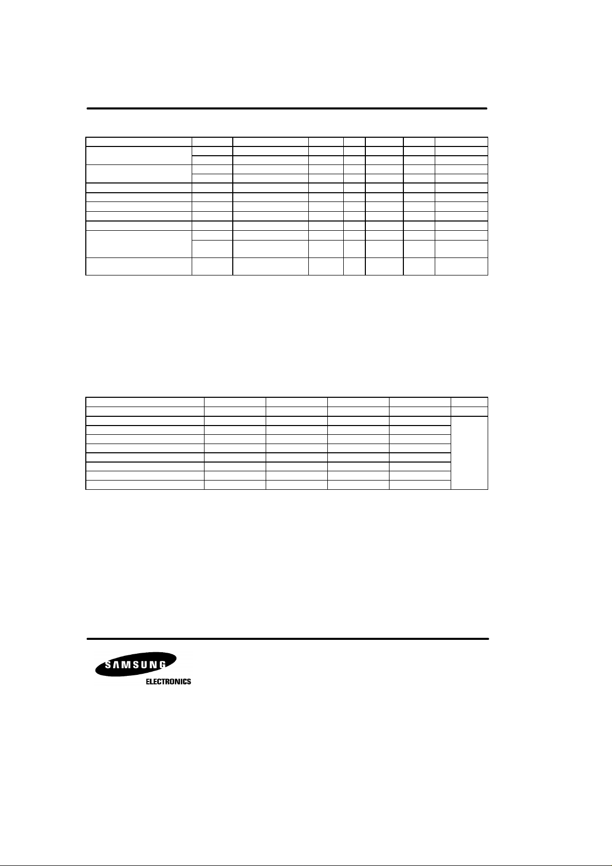
MAXIMUM ABSOLUTE LIMIT
Characteristic Symbol Value Unit Note
Operating Voltage V
Supply Voltage V
Driver Supply Voltage V
Operating Temperature T
Storage Temperature T
*1. Based on VSS=0V.
*2. Applies the same supply voltage to V
*3. Applies to M, FRM, CL, RSTB, ADC, CLK1, CLK2, CS1B, CS2B, CS3, E, R/W, RS and DB0~DB7.
*4. Applies V0L(R), V2L(R), V3L(R) and V5L(R).
Voltage level: VDD≥V0L=VOR≥V2L=V2R≥V3L=V3R≥V5L=V5R≥VEE.
V
LCD
OPR
STG
DD
EE
Display RAM data 1:ON
Display RAM data 0:OFF
(Relation of display RAM data & M)
M DATA Output Level
L L V
H V
H L V
H V
2
0
3
5
When RSTB=L,
(1) ON/OFF register becomes set by 0. (display off)
(2) Display start line register becomes set by 0
(Z-address 0 set, display from line 0)
After releasing reset, this condition can be changed only by instruction.
-0.3~+7.0 V *1
VDD-19.0~VDD+0.3 V *4
B
EE1
and V
EE2
-0.3~VDD+0.3 V *1,3
VEE-0.3~VDD+0.3 V *2
. V
LCD=VDD-VEE
-30~+85
-55~+125
.
°C
°C
KS0108B 64 CH SEGMENT DRIVER FOR DOT MATRIX LCD
ELECTRICAL CHARACTERISTICS
DC Characteristics (VDD=4.5~5.5V, VSS=0V, VDD-VEE=8~17V, Ta=-30~+85°C)
Characteristic Symbol Condition Min Typ Max Unit Note
Input High Voltage V
Input Low Voltage V
Output High Voltage V
Output Low Voltage V
Input Leakage Current I
Three-state(OFF) Input Current I
Driver Input Leakage Current I
Operating Current I
On Resistance R
IH1
V
IH2
IL1
V
IL2
IOH=-200µA
OH
OLIOL
VIN=VSS~V
LKG
VIN=VSS~V
TSL
VIN=VEE~V
DIL
During Display - - 100
DD1
I
During Access
DD2
Access Cycle=1MHz
VDD-VEE=15V
ON
¡¾I
*1. CL, FRM, M, RSTB, CLK1, CLK2
2. CS1B, CS2B, CS3, E, R/W, RS, DB0~DB7
3. DB0~DB7
4. Excepted DB0~DB7
5. DB0~DB7 at High lmpedance
6. V0L(R), V2L(R), V3L(R), V5L(R)
7. 1/64 duty, FCLK=250KHZ, Frame Frequency=70HZ, Output: No Load
8. VDD~VEE=15.5V
V0L(R)>V2L(R)=VDD-2/7 (VDD-VEE)>V3L(R)=VEE+2/7(VDD-VEE)>V5L(R)
- 0.7V
- 2.0 - V
- 0 - 0.3V
- 0 - 0.8 V *2
- V
DD
DD
DD
DD
V *1
V *2
V *1
2.4 - - V *3
=1.6mA - - 0.4 V *3
DD
DD
DD
-1.0 - 1.0
-5.0 - 5.0
-2.0 - 2.0
µA
µA
µA
µA
LOAD
- - 500
- - 7.5
=0.1mA
µA
KΩ
*4
*5
*6
*7
*7
*8
AC Characteristics (V
=5V±10%, VSS=0V, Ta=-30°C~+85°C)
DD
(1) Clock Timing
Characteristic Symbol Min Typ Max Unit
CLK1, CLK2 Cycle Time t
CLK1 ‘LOW’ Level Width t
CLK2 ‘LOW’ Level Width t
CLK1 ‘HIGH’ Level Width t
CLK2 ‘HIGH’ Level Width t
CLK1-CLK2 Phase Difference t
CLK2-CLK1 Phase Difference t
CLK1, CLK2 Rise Time t
CLK1, CLK2 Fall Time t
WL1
WL2
WH1
WH2
D12
D21
CY
2.5 - 20
µS
625 - -
625 - 1875 - - ns
1875 - -
625 - -
625 - -
R
F
- - 150
- - 150
 Loading...