

Samsung KS0094 Datasheet
34 COM / 80 SEG DRIVER & CONTROLLER FOR STN LCD
KS0094
written permission of LCD Driver IC Team.
Nov.1999.
Ver. 0.4
Prepared by: Won-Sik, Kang
K2w3@samsung.co.kr
Contents in this document are subject to change without notice. No part of this document may be reproduced
or transmitted in any form or by any means, electronic or mechanical, for any purpose, without the express

34 COM / 80 SEG DRIVER & CONTROLLER FOR STN LCD PRELIMINARY SPEC. VER. 0.4 KS0094
KS0094 Specification Revision History
Version Content Date
0.0 Original Apr.1999
CGROM font table added at table 5
COM data shift direction changed at table 9
0.1
Read data instruction separation according to RE bit at table 10
May.1999
Symbol register is changed to ICONRAM at table 12
IDD1 is changed at table 18, 19
0.2 IDD1 is changed at table 18, 19 Jun.1999
0.3 Pad location added at table 1 and 2 July.1999
0.4 VDD change (2.4V~5.5V -> 2.4V~3.6V) Nov.1999
1

KS0094 PRELIMINARY SPEC. VER. 0.4 34 COM / 80 SEG DRIVER & CONTROLLER FOR STN LCD
CONTENTS
INTRODUCTION.......................................................................................................................................... 1
FEATURES ................................................................................................................................................. 1
BLOCK DIAGRAM ...................................................................................................................................... 3
PAD CONFIGURATION .............................................................................................................................. 4
PAD CENTER COORDINATES ..................................................................................................................5
PIN DESCRIPTION...................................................................................................................................... 6
POWER SUPPLY.................................................................................................................................6
LCD DRIVER SUPPLY......................................................................................................................... 6
SYSTEM CONTROL............................................................................................................................. 7
MPU INTERFACE ................................................................................................................................ 8
LCD DRIVER OUTPUTS...................................................................................................................... 8
TEST....................................................................................................................................................8
FUNCTION DESCRIPTION.......................................................................................................................... 9
SYSTEM INTERFACE..........................................................................................................................9
ADDRESS COUNTER (AC)................................................................................................................ 13
DISPLAY DATA RAM (DDRAM)......................................................................................................... 13
CHARACTER GENERATOR ROM (CGROM)..................................................................................... 13
CHARACTER GENERATOR RAM (CGRAM) ..................................................................................... 19
SEGMENT ICON RAM (ICONRAM).................................................................................................... 20
HIGH POWER MODE......................................................................................................................... 22
LOW POWER CONSUMPTION MODE .............................................................................................. 22
LCD DRIVER CIRCUIT....................................................................................................................... 23
INSTRUCTION DESCRIPTION .................................................................................................................. 24
INITIALIZING & POWER SAVE MODE SETUP......................................................................................... 35
HARDWARE RESET.......................................................................................................................... 35
INITIALIZING AND POWER SAVE SETUP......................................................................................... 37
LCD DRIVING POWER SUPPLY CIRCUIT................................................................................................ 40
VOLTAGE CONVERTER.................................................................................................................... 40
VOLTAGE REGULATOR .................................................................................................................... 41
ELECTRONIC CONTRAST CONTROL (32 STEPS)........................................................................... 42
VOLTAGE GENERATOR CIRCUIT .................................................................................................... 44
MPU INTERFACE...................................................................................................................................... 45
APPLICATION INFORMATION FOR LCD PANEL.................................................................................... 47
FRAME FREQUENCY............................................................................................................................... 51
MAXIMUM ABSOLUTE RATINGS............................................................................................................. 52
ELECTRICAL CHARACTERISTICS.......................................................................................................... 53
DC CHARACTERISTICS.................................................................................................................... 53
AC CHARACTERISTICS.................................................................................................................... 54
2

34 COM / 80 SEG DRIVER & CONTROLLER FOR STN LCD PRELIMINARY SPEC. VER. 0.4 KS0094
INTRODUCTION
The KS0094 is an LCD driver and controller LSI for liquid crystal dot matrix character display systems. It can
display 2, 3 or 4 lines of 16 characters with 5 x 8 dots format. It is capable of interfacing various microprocessors,
supporting the 4-bit, 8-bit parallel modes and the clock synchronized serial mode. Voltage converter, oscillator,
voltage regulator, voltage follower and bias circuit are built in the IC. The double height character mode and line
vertical scroll functions are supported.
FEATURES
Driver Outputs
- Common outputs: 34 common
- Segment outputs: 80 segment
Applicable Panel Size
Font Display Duty Contents of outputs
2-line x 16 characters 1 / 18 2 x 16 characters + 160 icons
5 x 8
3-line x 16 characters 1 / 26 3 x 16 characters + 160 icons
4-line x 16 characters 1 / 34 4 x 16 characters + 160 icons
Internal Memory
- Character Generator ROM (CGROM): 21,760 bits (544 characters x 5 x 8 dots)
- Character Generator RAM (CGRAM): 240 bits (6 characters x 5 x 8 dots)
- Display Data RAM (DDRAM): 640 bits (16 characters x 5 lines )
- Segment Icon RAM (ICONRAM): 160 bits (160 icons)
MPU Interface
- No busy MPU interface (no busy check or no execution waiting time)
- 8-bit parallel interface mode: 68-series and 80-series are available
- 4-bit parallel interface mode: 68-series and 80-series are available
- Serial interface mode: 4-pin clock synchronized serial interface
Function Set
- Various instructions set: display control, power save, power control, etc.
- COM / SEG bi-directional ( 4-type LCD application available)
- H/W reset (RESETB)
Built-in Analog Circuit
- Internal RC oscillator circuit or external clock
- Electronic volume for contrast control (32 steps)
- Voltage converter / voltage regulator / voltage follower & bias circuit
Low Power Operation
- Sleep mode operation (5uA Max.)
- Normal mode operation (TBD)
1

KS0094 PRELIMINARY SPEC. VER. 0.4 34 COM / 80 SEG DRIVER & CONTROLLER FOR STN LCD
Operating Voltage Range
- Power supply voltage (VDD): 2.2V – 3.6V
- LCD driving voltage (VLCD = V0 - VSS): 7.0V Max.
Package Type
- Gold bumped chip
2
34 COM / 80 SEG DRIVER & CONTROLLER FOR STN LCD PRELIMINARY SPEC. VER. 0.4 KS0094
(DR)
BLOCK DIAGRAM
RESETB
PS
IF
M I
CSB
RS
RW_WR
E_RD
DB7
(SI)
DB6
(SCL)
DB5-
DB4
DB3-
DB0
DUTY1
DUTY0
Parallel
Interface
4 bit/8 bit
Serial
Interface
Input Buffer
8
8
8
8
Icon
RAM
160 bits
Instruction
Register
(IR)
Address
Counter
Data
Register
Data Output
Register
(OR)
Character
Generator
RAM
(CGRAM)
240 bits
CK
Instruction
Decoder
Data RAM
(DDRAM)
7
8
8
Character
Generator
ROM
(CGROM)
21760 bits
Display
640 bits
8
8
Timing GeneratorOscillator
Cursor
and
Blink
Controller
80 bits
Shift
Register
34 bits
Shift
Register
80 bits
Latch
Circuit
Common
Driver
Segment
Driver
LCD
Driver
Voltage
Selector
COM1-
COM32
COM I1
COM I2
SEG1-
SEG80
5 5
V
DD
GND
Voltage Converter Voltage Regulator Voltage Follower & Bias Resistor
CAP1+ CAP1- CAP2+ CAP2- VOUT V0 VR V1 V2 V3 V4 DIRS
Segment Data Conversion
LCD Driving Power Circuit
Figure 1. Block Diagram
3
KS0094 PRELIMINARY SPEC. VER. 0.4 34 COM / 80 SEG DRIVER & CONTROLLER FOR STN LCD
............................
...
...
1
61
82
163
42
µ
m
108
µ
m
42
µ
m
108
µ
m
30µm
30µm
30µm
(-2830, -835)
60µm
30µm
(-3110, +880)
(+3110, +880)
PAD CONFIGURATION (NOT FIXED)
164
183
Y
(0,0)
X
...........................
DUMMY PAD
PAD
Figure 2. Pad Configuration
Table 1. KS0094 Pad Dimensions
Item Pad No.
Chip size - 6320 1860
1 – 66 90
63~80,83~162,165~182 70Pad pitch
62,81,82,163,164,183 90
1~61 60 100
63~80 100 50
83~162 50 100
Bumped pad size
165~182 100 50
62,81 100 60
82,163 60 100
164,183 100 60
Bumped pad height All pad 17 (Typ.)
Size
X Y
81
62
Unit
µm
COG Align Key Coordinate ILB Align Key Coordinate
30µm 30µm 30µm
4
30µm 30µm 30µm
(+2830, -830)
42µm 108µm
42µm 108µm

34 COM / 80 SEG DRIVER & CONTROLLER FOR STN LCD PRELIMINARY SPEC. VER. 0.4 KS0094
Pad
Pad
Pad
Pad
Pad
Pad
No
Name
No
Name
No
Name
1RS-2700
-820
62
DUMMY1
3050
-700
123
SEG41
-35
820
2
VSS
-2610
-820
63
COMI1
3050
-620
124
SEG42
-105
820
3
RW_WR
-2520
-820
64
COM1
3050
-550
125
SEG43
-175
8204VDD
-2430
-820
65
COM2
3050
-480
126
SEG44
-245
820
5
E_RD
-2340
-820
66
COM3
3050
-410
127
SEG45
-315
820
6
VSS
-2250
-820
67
COM4
3050
-340
128
SEG46
-385
8207CSB
-2160
-820
68
COM5
3050
-270
129
SEG47
-455
8208DB7
-2070
-820
69
COM6
3050
-200
130
SEG48
-525
8209DB6
-1980
-820
70
COM7
3050
-130
131
SEG49
-595
82010DB5
-1890
-820
71
COM8
3050
-60
132
SEG50
-665
82011DB4
-1800
-820
72
COM9
3050
10
133
SEG51
-735
82012DB3
-1710
-820
73
COM10
3050
80
134
SEG52
-805
82013DB2
-1620
-820
74
COM11
3050
150
135
SEG53
-875
82014DB1
-1530
-820
75
COM12
3050
220
136
SEG54
-945
82015DB0
-1440
-820
76
COM13
3050
290
137
SEG55
-1015
820
16
VDD
-1350
-820
77
COM14
3050
360
138
SEG56
-1085
820
17
VDD
-1260
-820
78
COM15
3050
430
139
SEG57
-1155
82018VSS
-1170
-820
79
COM16
3050
500
140
SEG58
-1225
82019VSS
-1080
-820
80
COMI1
3050
570
141
SEG59
-1295
820
20V4-990
-820
81
DUMMY2
3050
650
142
SEG60
-1365
820
21V4-900
-820
82
DUMMY3
2845
820
143
SEG61
-1435
82022V3
-810
-820
83
SEG1
2765
820
144
SEG62
-1505
82023V3
-720
-820
84
SEG2
2695
820
145
SEG63
-1575
820
24V2-630
-820
85
SEG3
2625
820
146
SEG64
-1645
820
25V2-540
-820
86
SEG4
2555
820
147
SEG65
-1715
82026V1
-450
-820
87
SEG5
2485
820
148
SEG66
-1785
82027V1
-360
-820
88
SEG6
2415
820
149
SEG67
-1855
820
28V0-270
-820
89
SEG7
2345
820
150
SEG68
-1925
820
29V0-180
-820
90
SEG8
2275
820
151
SEG69
-1995
82030V0
-90
-820
91
SEG9
2205
820
152
SEG70
-2065
82031V00-820
92
SEG10
2135
820
153
SEG71
-2135
820
32VR90
-820
93
SEG11
2065
820
154
SEG72
-2205
820
33VR180
-820
94
SEG12
1995
820
155
SEG73
-2275
82034VSS
270
-820
95
SEG13
1925
820
156
SEG74
-2345
82035DUTY1
360
-820
96
SEG14
1855
820
157
SEG75
-2415
820
36
VDD
450
-820
97
SEG15
1785
820
158
SEG76
-2485
820
37
DUTY0
540
-820
98
SEG16
1715
820
159
SEG77
-2555
82038VSS
630
-820
99
SEG17
1645
820
160
SEG78
-2625
82039VOUT
720
-820
100
SEG18
1575
820
161
SEG79
-2695
820
40
VOUT
810
-820
101
SEG19
1505
820
162
SEG80
-2765
820
41
CAP2-
900
-820
102
SEG20
1435
820
163
DUMMY4
-2845
82042CAP2-
990
-820
103
SEG21
1365
820
164
DUMMY5
-3050
65043CAP2+
1080
-820
104
SEG22
1295
820
165
COMI2
-3050
57044CAP2+
1170
-820
105
SEG23
1225
820
166
COM32
-3050
50045CAP1-
1260
-820
106
SEG24
1155
820
167
COM31
-3050
43046CAP1-
1350
-820
107
SEG25
1085
820
168
COM30
-3050
36047CAP1+
1440
-820
108
SEG26
1015
820
169
COM29
-3050
29048CAP1+
1530
-820
109
SEG27
945
820
170
COM28
-3050
22049VSS
1620
-820
110
SEG28
875
820
171
COM27
-3050
15050DIRS
1710
-820
111
SEG29
805
820
172
COM26
-3050
80
51
VDD
1800
-820
112
SEG30
735
820
173
COM25
-3050
10
52CK1890
-820
113
SEG31
665
820
174
COM24
-3050
-6053VSS
1980
-820
114
SEG32
595
820
175
COM23
-3050
-130
54PS2070
-820
115
SEG33
525
820
176
COM22
-3050
-200
55
VDD
2160
-820
116
SEG34
455
820
177
COM21
-3050
-270
56IF2250
-820
117
SEG35
385
820
178
COM20
-3050
-340
57
VSS
2340
-820
118
SEG36
315
820
179
COM19
-3050
-410
58MI2430
-820
119
SEG37
245
820
180
COM18
-3050
-480
59
VDD
2520
-820
120
SEG38
175
820
181
COM17
-3050
-550
60
RESETB
2610
-820
121
SEG39
105
820
182
COMI2
-3050
-620
61
TEST
2700
-820
122
SEG40
35
820
183
DUMMY6
-3050
-700
PAD CENTER COORDINATES
Table 2. Pad Center Coordinates [Unit: µm]
X YX Y X Y
5
KS0094 PRELIMINARY SPEC. VER. 0.4 34 COM / 80 SEG DRIVER & CONTROLLER FOR STN LCD
PIN DESCRIPTION
POWER SUPPLY
Table 3. Pin Description
Name I/O Description
VDD
VSS
V0
V1
V2
V3
V4
LCD DRIVER SUPPLY
Power
I/O
Power supply
Connect to MPU power supply pin
0V (GND)
Bias voltage level for LCD driving
Voltages should have the following relationship;
V0 ≥ V1 ≥ V2 ≥ V3 ≥ V4 ≥ VSS
When the built-in power circuit is active and internal 1/5 bias resistors
are used.
LCD bias V1 V2 V3 V4
1/5 bias
When the built-in power circuit is active and internal 1/4 bias resistors
are used.
LCD bias V1 V2 V3 V4
1/4 bias (3/4) x V0 (2/4) x V0
(4/5) x V0 (3/5) x V0
(2/5) xV0(1/5) x
V0
(1/4) x
V0
Table 3. Pin Description (Continued)
Name I/O Description
CAP1+ O Capacitor + connecting pin for the internal voltage converter
CAP1- O Capacitor - connecting pin for the internal voltage converter
CAP2+ O Capacitor + connecting pin for the internal voltage converter
CAP2- O Capacitor - connecting pin for the internal voltage converter
VOUT I/O DC/DC voltage converter output
Voltage adjust pin
VR I
6
This pin gives a voltage between V0 and VSS by resistance-division of
voltage.
34 COM / 80 SEG DRIVER & CONTROLLER FOR STN LCD PRELIMINARY SPEC. VER. 0.4 KS0094
SYSTEM CONTROL
Table 3. Pin Description (Continued)
Name I/O Description
External clock input
CK I
MI I
PS I
IF I
DIRS I
It must be fixed to "High" or "Low" when the internal oscillation circuit is used.
In case of the external clock mode, CK is used as the clock and OS bit
should be OFF.
MPU interface selection input
MI = "Low": 80 series MPU
MI = "High": 68 series MPU
Parallel / Serial selection input
When PS = "Low": Serial mode
When PS = "High": 4-bit/8-bit bus mode
Interface data length selection pin for parallel data input
When PS = "Low"
IF = "Low" or "High": serial interface mode
When PS = “High”
IF = "Low": 4-bit bus mode
IF = "High": 8-bit bus mode
SEG direction selection input
When DIRS = "Low”
SEG1 → SEG2 → SEG79 → SEG80
When DIRS = "High”
SEG80 → SEG79 → SEG2 → SEG1
Display line mode selection input
DUTY1
DUTY0
DUTY1 DUTY0 Mode Duty
0 0 2-line 1/18
I
0 1 3-line 1/26
1 0/1 4-line 1/34
7
KS0094 PRELIMINARY SPEC. VER. 0.4 34 COM / 80 SEG DRIVER & CONTROLLER FOR STN LCD
MPU INTERFACE
Table 3. Pin Description (Continued)
Name I/O Description
RESETB I
CSB I
RS I
RW_WR I
E_RD I
DB0 - DB3
DB4 - DB5
DB6 (SCL),
DB7 (SI)
I/O
Reset input
KS0094 is initialized while RESETB is low.
Chip selection input
KS0094 is selected while CSB is low.
Register selection input
When RS = "Low", instruction register
When RS = "High", data register
In 80-series MPU interface mode
This pin is connected to WR pin of MPU and is an active low write signal.
In 68-series MPU interface mode
This pin is connected to R/W pin of MPU.
When RW_WR = "Low", write mode
When RW_WR = "High", read mode
In 80-series MPU interface mode
This pin is connected to RD pin of MPU and is a active low read signal.
In 68-series MPU interface mode
This pin is connected to E pin of MPU and enable read or write command
according to RW_WR signal.
When 8-bit bus mode, used as bi-directional data bus DB0 - DB7.
During 4-bit bus mode, only DB4 - DB7 are used. In this case DB0 - DB3 pins
are not used.
When serial mode, DB6 (SCL) is used as serial clock input pin and DB7 (SI)
is used as serial data input pin.
LCD DRIVER OUTPUTS
Name I/O Description
COM1 – COM32 O Common signal output for driving LCD
COMI1, COMI2 O Common signal output for icon display
SEG1 – SEG80 O Segment signal output for driving LCD
TEST
Name I/O Description
TEST I
NOTE: DUMMY – These pins should be opened (floated).
Test pin
This pin is not used for normal operation. Open at normal operation mode
8
34 COM / 80 SEG DRIVER & CONTROLLER FOR STN LCD PRELIMINARY SPEC. VER. 0.4 KS0094
FUNCTION DESCRIPTION
SYSTEM INTERFACE
KS0094 has two kinds of interface type with MPU: bus mode, serial mode. Serial or bus mode is selected by PS
pin. In bus mode, 4-bit bus or 8-bit bus is selected by IF pin, and 68 series MPU or 80 series MPU is selected by
MI pin.
Table 4. Various Kinds of MPU Interface according to PS, MI and IF
PS MI IF CSB RS RW_WR E_RD DB0∼∼DB3 DB4∼∼DB5 DB6 DB7
68 series
Bus
mode (H)
Serial
mode (L)
NOTES:
1. ‘ * ‘: Don’t care (High, Low or Open)
2. ‘ (H)/(L) ‘: Fixed High (VDD) or Low (VSS)
(H)
80 series
(L)
(H)/(L)
8 bit (H) CSB RS R/W E DB0∼DB3 DB4∼DB5 DB6 DB7
4 bit (L) CSB RS R/W E ∗
8 bit (H) CSB RS WR RD DB0∼DB3 DB4∼DB5 DB6 DB7
4 bit (L) CSB RS WR RD
(2)
(H)/(L) CSB RS (H)/(L) (H)/(L)
(1)
∗
∗ ∗
DB4∼DB5 DB6 DB7
DB4∼DB5 DB6 DB7
SCL SI
PS: "High" = bus mode, "Low" = serial mode
MI: "High" = 68-series MPU, "Low" = 80-series MPU
IF: "High" = 8-bit mode, "Low" = 4-bit mode (PS: "High")
CSB: "High" = chip is not selected, "Low" = chip is selected
RS: "High" = data register, "Low" = instruction register
RW_WR: read / write indicating signal in 68 mode or active low signal for enabling write in 80 mode.
E_RD: active high signal for enabling command is 68 mode or active low signal for enabling read in 80 mode.
SCL (DB6): serial clock input
SI (DB7): serial data input
9
KS0094 PRELIMINARY SPEC. VER. 0.4 34 COM / 80 SEG DRIVER & CONTROLLER FOR STN LCD
MI
CSB
RS
RW_WR
E_RD
DB7-DB0
Data
IF
Interface with MPU in Parallel Mode (PS = "High")
During writing operation, two 8-bit registers, data register (DR) and instruction register (IR), are used. The data
register (DR) is used as temporary data storage place for being written into DDRAM / CGRAM / ICONRAM and
one of these RAM is selected by RAM address setting instruction. The Instruction register (IR) is used only to
store instruction code transferred from MPU. To select DR or IR register, RS input pin is used.
During reading operation, 8-bit register, output data register (OR) is used. The output data register (OR) is used
as temporary data storage place for being read from DDRAM / CGRAM / ICONRAM and one of these RAM is
selected by RAM address setting instruction. After RAM address setting, first reading is a dummy cycle in 8-bit
bus mode (figure 3, 4). The valid data comes from second reading. In 4-bit bus mode, after RAM address setting,
first and second reading are dummy cycles (figure 5, 6). The valid data comes from third reading. The dummy
read make the address counter (AC) increased by 1. So it is recommended to set address again before writing.
The instruction read cycle is not supported and it is regarded as a no operation cycle.
In 4-bit bus mode, it is needed to transfer 4-bit data (through DB7-DB4) by two times. The high order bits (for 8-bit
mode DB7-DB4) are written before the low order bits (for 8-bit mode DB3-DB0) in write and low order bits (for 8-bit
mode DB3-DB0) are read before the high order bits (for 8-bit mode DB7-DB4) in read transaction. The DB0-DB3
pins are floated in this 4-bit bus mode. After RESETB resets, KS0094 considers first 4-bit data from MPU as the
high order bits.
Valid
Instruction
Write
NOP RAM
Dummy
Read
Read
Data
Write
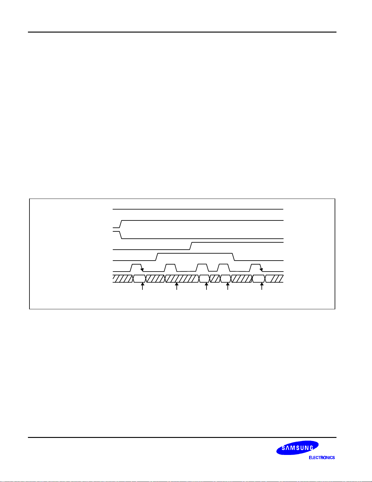
Figure 3. Timing Diagram of 8-bit Parallel Bus Mode Data Transfer (68-series MPU Mode)
10
34 COM / 80 SEG DRIVER & CONTROLLER FOR STN LCD PRELIMINARY SPEC. VER. 0.4 KS0094
MI
CSB
RS
RW_WR
E_RD
DB7-DB0
Data
MI
CSB
RS
RW_WR
E_RD
DB7-DB4
4-bit
4-bit
4-bit
4-bit
4-bit
4-bit
IF
MI
CSB
RS
RW_WR
E_RD
DB7-DB4
4-bit
4-bit
4-bit
4-bit
4-bit
4-bit
IF
IF
Valid
Instruction
Write
NOP RAM
Dummy
Read
Read
Data
Write
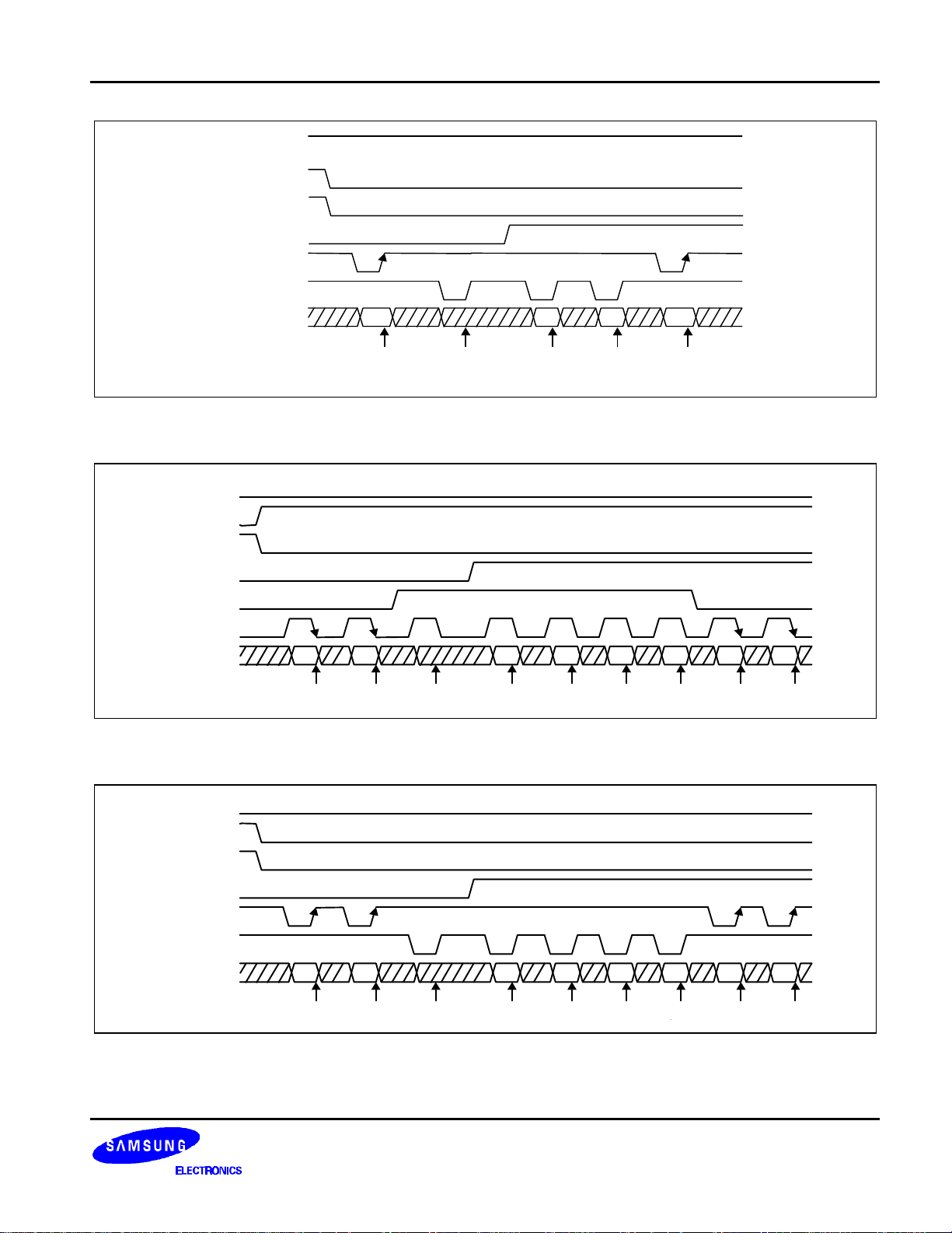
Figure 4. Timing Diagram of 8-bit Parallel Bus Mode Data Transfer (80-series MPU Mode)
upper
lower
upper
Instruction Write Dummy Read Data WriteNOP RAM Read
lower
upper
lower
Figure 5. Timing Diagram of 4-bit Parallel Bus Mode Data Transfer (68-series MPU Mode)
upper
lower
upper
lower
upper
lower
Instruction Write Dummy Read Data WriteNOP RAM
Figure 6. Timing Diagram of 4-bit Parallel Bus Mode Data Transfer (80-series MPU Mode)
11
KS0094 PRELIMINARY SPEC. VER. 0.4 34 COM / 80 SEG DRIVER & CONTROLLER FOR STN LCD
RS
D7D6D5D4D3D2D1D0D7
123456789
Interface with MPU in Serial Mode (PS = "Low")
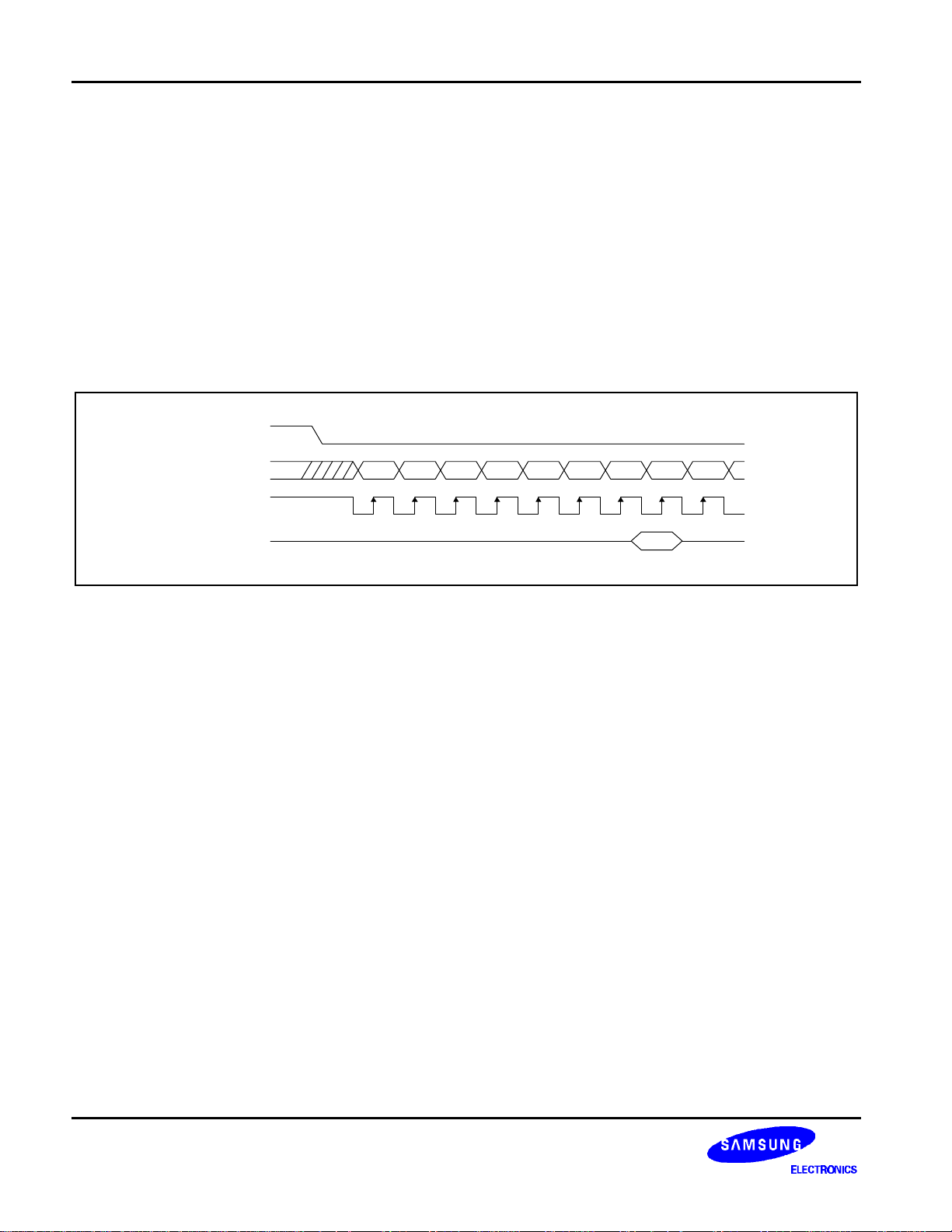
When PS input pin is "Low", clock synchronized serial interface mode is selected. At this time, four ports, SCL
(DB6, synchronizing transfer clock), SI (DB7, serial input data), RS (register selection input) and CSB (chip
selection input) are used.
By setting CSB to "Low", KS0094 can receive SCL input. If CSB is set to "High", KS0094 resets the internal 8-bit
shift register and 3-bit counter. Serial data is input in the order of "D7, D6, D5, D4, D3, D2, D1, D0" from the serial
data input pin (SI = DB7) at the rising edge of serial clock (SCL = DB6).
At the rising edge of the 8th serial clock, the serial data (D7-D0) is converted into 8 bit bus mode data. The RS
input of the DR/IR selection is latched at the rising edge of the 8th serial clock (SCL).
In serial mode, the read is not possible.
CSB
SI (DB7)
SCL (DB6)
Figure 7. Timing Diagram of Serial Data Transfer
12

34 COM / 80 SEG DRIVER & CONTROLLER FOR STN LCD PRELIMINARY SPEC. VER. 0.4 KS0094
ADDRESS COUNTER (AC)
Address Counter (AC) in KS0094 stores DDRAM / CGRAM / ICONRAM address. After writing into or reading from
DDRAM / CGRAM / ICONRAM, AC is automatically increased by 1. The address counter is only one and stores
the address among DDRAM / CGRAM / ICONRAM.
DISPLAY DATA RAM (DDRAM)
DDRAM stores display data of maximum 80 x 8 bits (Max. 80 characters). DDRAM address is set in the address
counter (AC) as a hexadecimal number.
1st Ch. 16th Ch.
COM1 ∼ COM8
COM9 ∼ COM16
COM17 ∼ COM24
COM25 ∼ COM32
Hidden Line
SEG1 SEG80
34 35 36 37 38 3 9 3A 3B 3C 3D 3E 3F30 3 1 32 33
44 45 46 47 48 4 9 4A 4B 4C 4D 4E 4F40 4 1 42 43
54 55 56 57 58 5 9 5A 5B 5C 5D 5E 5F50 5 1 52 53
64 65 66 67 68 6 9 6A 6B 6C 6D 6E 6F60 6 1 62 63
74 75 76 77 78 7 9 7A 7B 7C 7D 7E 7F70 7 1 72 73
DDRAM Address in 4 line Display
Figure 8. DDRAM Address
CHARACTER GENERATOR ROM (CGROM)
CGROM has one main ROM and four option ROM. The main CGROM has 160 characters and the option
CGROMs have 96 characters each. The total CGROM has 5 x 8-dot 544 characters. The R1, R0 bits select an
option CGROM between 4 option CGROM. If one of 4 CGROM is selected, the other CGROM font can not be
used. The CG bit of the instruction table selects the 6 characters (00h ∼ 05h) of CGROM or CGRAM.
13
KS0094 PRELIMINARY SPEC. VER. 0.4 34 COM / 80 SEG DRIVER & CONTROLLER FOR STN LCD
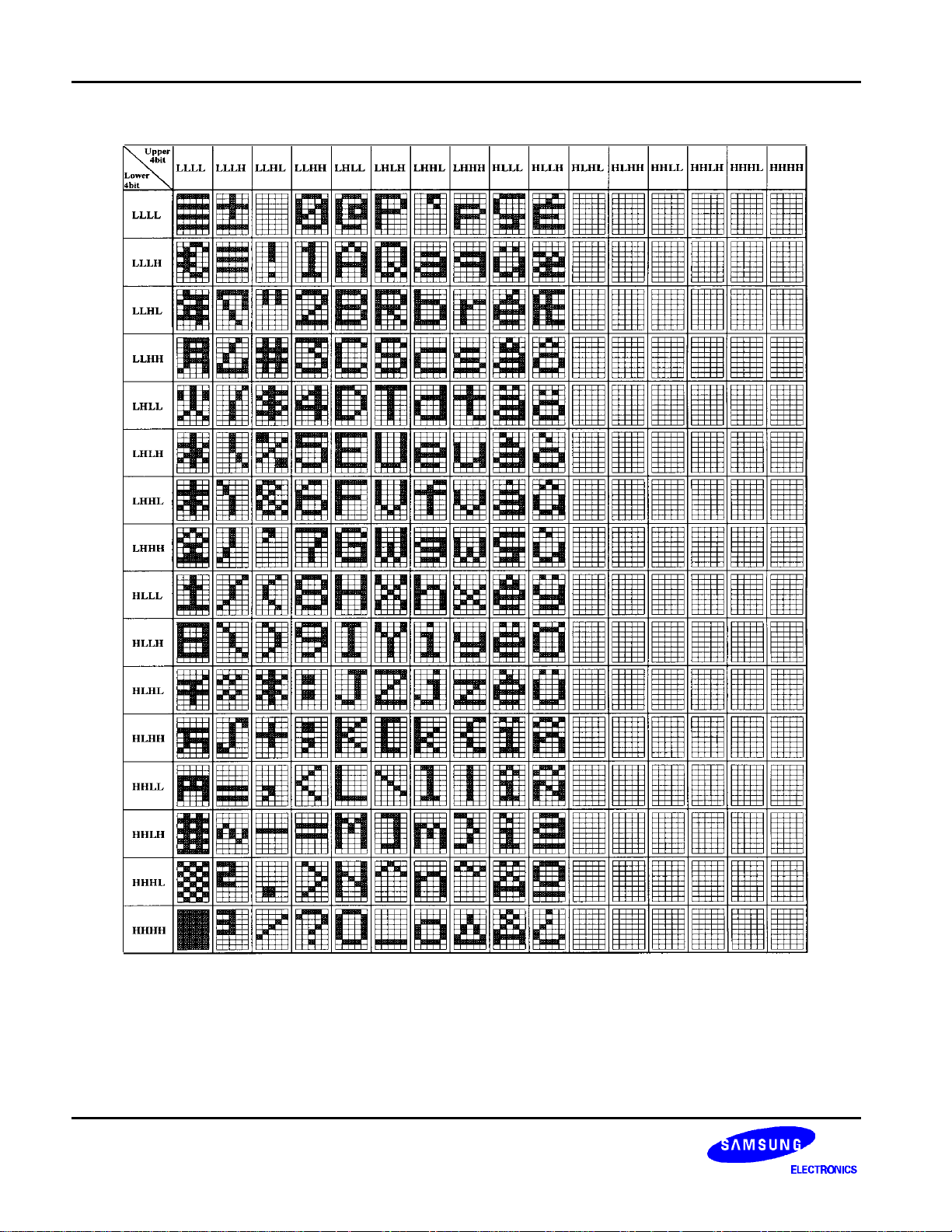
Table 5. CGROM Character Code (Main ROM)
14

34 COM / 80 SEG DRIVER & CONTROLLER FOR STN LCD PRELIMINARY SPEC. VER. 0.4 KS0094
Table 5. CGROM Character Code (Option ROM1) (Continued)
15
 Loading...