

Samsung KS0068B Datasheet
KS0068B 16COM/60SEG DRIVER & CONTROLLER FOR DOT MATRIX LCD
INTRODUCTION
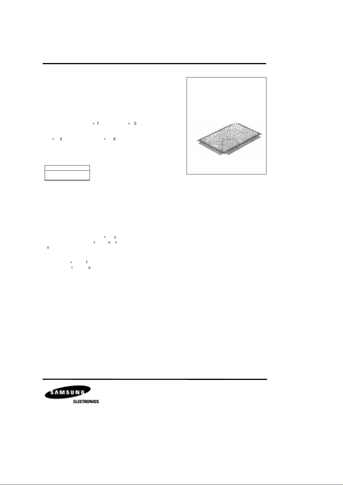
100 QFP
The KS0068B is a dot matrix LCD driver & controller LSl which is
fabricated by low power CMOS technology.
FUNCTION
• Character type dot matrix LCD driver & controller
• Internal driver: 16 common and 60 segment signal output.
• Display character format; 57 dots + cursor, 510 dots + cursor
• Easy interface with a 4-bit or 8-bit MPU
• Display character pattern:
57 dots format: 192 kinds, 510 dots format: 32kinds
• The special character pattern can be programmable by
Character Generator RAM directly.
• A customer character pattern can be programmable by mask
option (KS0068B-00; Standard type)
KS0068B-0 0
English, Japanese
Numberal
• Automatic power on reset function.
• It can drive a maximum 80 characters by using the kS0065B
or KS0063B, KS0068B externally.
• It is possible to read both Character Generator and Display
Data RAM from MPU.
FEATURES
• Internal Memory
- Character Generator ROM: 8320bits
- Character Generator RAM: 512 bits
- Display Data RAM: 808bits for 80 digits.
• Power Supply Voltage; +5Vä10%, +3Vä10%
• Supply voltage for display: 0~-5V(V
• CMOS process
• 1/8 duty, 1/11 duty or 1/16 duty: selectable
(1/8 duty; 57 dots format 1 line, 1/11 duly; 5 x 10 dots format I line,
1/16 duty: 57 dots format 2 line)
• 100 QFP or bare chip available.
)
5

KS0068B 16COM/60SEG DRIVER & CONTROLLER FOR DOT MATRIX LCD
BLOCK DIAGRAM
5
Parallel/Serial
Data conversion
Circuit
5
Power
supply
for
LCD
Drive
V1
V2
V3
V4
V5
DB0 ~ DB
DB4 ~ DB
R/W
OSC
1
OSC
2
7
7
Cursor
Blink
Control
Circuit
8
Display
Data RAM
( DD RAM )
8038 bits
60 - bit
Shift
Register
segment
signal
( S
- S60 )
60 - bit
60
Latch
Circuit
60
Segment
Signal
Driver
1
60
D
Busy
Flag
Charater
Generator
ROM
( CG ROM )
Data
Register
( DR )
Instruction
Register
8320 bits
8
7
8
4
3
4
7
Input
8
Output
Buffer
RS
8
E
( IR )
Character
Generator
RAM
( CG RAM )
512 bits
8
Instruction
Decoder
( ID )
7
7
common
signal
( C1 - C16 )
16 - bit
Shift
Register
16
Common
Signal
Driver
16
CLK1
CLK2
M
V
GND
DD
Address
Counter
( AC )
7
Timing
Generation
Circuit
Fig. 1. KS0068 functional block diagram.

KS0068B 16COM/60SEG DRIVER & CONTROLLER FOR DOT MATRIX LCD
PIN CONFIGURATION
S47S48S49S50S51S52S53S54S55S56S57S58S59S60C16C15C14C13C12C11C10C9C8C7C6C5C4C3C2C
80 79 78 77 76 75 74 73 72 71 70 69 68 67 66 65 64 63 62 61 60 59 58 57 56 55 54 53 52 51
S
81
46
S
82
45
S
83
44
S
84
43
S
85
42
86
S
41
87
S
40
88
S
39
89
S
38
S
90
37
S
91
36
S
92
35
S
93
34
S
94
33
S
95
32
S
96
31
S
97
30
S
98
29
99
S
28
100
S
27
KS0068B
KS0068
1 2 3 4 5 6 7 8 9 10 11 12 13 14 15 16 17 18 19 20 21 22 23 24 25 26 27 28 29 30
S26S25S24S23S22S21S20S19S18S17S16S15S14S13S12S11S10S9S8S7S6S5S4S3S2S1VSSOSC2OSC1V
Fig2. 100QFP Top View
Fig2. 100QFP Top View
1
50
DB
7
49
DB
6
48
DB
5
47
DB
4
46
DB
3
45
DB
2
44
DB
1
43
DB
0
42
V
DD
41
E
40
R/W
39
RS
38
D
37
M
36
CLK
2
35
CLK
1
34
V
5
33
V
4
32
V
3
31
V
2
1
KS0068B 16COM/60SEG DRIVER & CONTROLLER FOR DOT MATRIX LCD
PIN DESCRIPTION
PIN(No). INPUT/OUTPUT NAME DESCRIPTION INTERFACE
VDD(42) Operating Voltage for logical circuit (2.7V ~ 5.5V) Power
VSS(GND) (27) Power 0V (GND) Supply
V1-V5(30-34) Negative Supply
Voltage
S1-S
60
(1-26, 67-100)
C1-C
16
(51-66)
OSC1, OSC
(29) (28)
2
Output Segment output Segent signal output for LCD driving LCD
Output Common output Common signal output for LCD driving LCD
Input (OSC1)
Output (OSC2)
Oscillator Both pin connected to Rf resistor or ceramic
CLK1 (35) Output Data latch clock Clock output terminal for the serially
CLK2 (36) Data shift clock Clock output terminal used when D terminal data
M (37) Alternated
signal for LCD
D (38) Display data
driver output
interface
E(41) Input Enable Start enable signal to read or write the data
R/W(40) Read/Write R/W signal input is used to select the read/write
Bias voltage level for LCD driving
resonator for internal oscillator circuit. In case of
external frequency use only, the frequency is input
to OSC1 terminal.
transfered data to be latched to the driver.
output shifts the inside of the driver.
The alternating signal to convert LCD
drive waveform to AC
Character pattern data, which is corresponding to
each common signal, is supplied to driver serially.
High Selection
Low Non selection
mode
High Read mode
Low Write mode
Resistor or
Ceramic
Resonator
KS0065B
or
KS0063B
MPU
RS (39) Register select register selection input
High Data register
(for read and write)
Low Instruction register (for write),
Busy flag, address counter
(for read)
DB0-DB
(43-50)
Input/Output Data interface Used for data transfer between the MPU and
7
KS0068. These terminals are for data bus with
bidirectional three-state.
Initial 4 bit (DB
operation (DB
-DB3) are not used during 4-bit
0
can be used as a busy flag)
7

KS0068B 16COM/60SEG DRIVER & CONTROLLER FOR DOT MATRIX LCD
Internal logic of input/output terminal
Input/Output Applicable pin
Input No
Pull
up
Logic diagram
E
with
pull
up
Output CLK1, CLK2
Input
Output
RS, R/W
M,D
DB0-DB
7
KS0068B 16COM/60SEG DRIVER & CONTROLLER FOR DOT MATRIX LCD
MAXIMUM ABSOLUTE LIMIT
(Ta=25Î)
Characteristic Symbol Value Unit
Operating Voltage
Driver Supply Voltage
Input Voltage
Power Dissipation
Operating Temperature
Storage Temperature
~
Voltage greater than above may damage to the circuit (VDD(
V
DD
V
LCD
V
IN
P
D
T
OPR
T
STG
V1(
V2(
-0.3~+7.0
V
-11.5~VDD+0.3
DD
-0.3 ~ V
-30~+85
-55~+125
V3(
V4(
500
V5)
DD
+0.3
mW
Î
Î
V
V
V
ELECTRICAL CHARACTERISTICS
(V
=+5V
ä
DC Characteristics
Characteristic Sy m bol Test condition Min Typ Max Unit Applicable Pin
DD
10%, V
Operating Voltage V
Operating Current (*1) I
Input Voltage 1 High V
Low V
Input Voltage 2 High V
Low V
Output Voltage 1 High V
Low V
Output Voltage 2 High V
Low V
Voltage Drop (*2) COM Vd
SEG Vd
Input Leakage Current I
Input Low Current I
External Clock Frequency(*3) f
Duty duty 455055%
Rise time t
Fall time t
Internal Clock Frequency(*3) f
Ceramic Resonator OSC Frequency
(*3)
LCD driving voltage(*4) V
Note: *1) Applies to the current value flown in terminal VDD when power is input as follows; VDD=5V, GND=0V, V1=3.4V,
V2=1.8V, V3=0.2V, V4=-1.4V and V5=-3V.
*2) Applied to the voltage drop occuring from terminals V
0.1mA is flown in or out to and from all COM and SEG terminals, and also to voltage drop occuring from terminals
V
out, while 0.1mA flow in when the output level is at V3, V4 or V5 level. This occurs when 5V or -5V is input to V
, V2, V3 and V5 to each SEG terminal (S1-S60). When the output level is at VDD, V1 or V2 level, 0.1mA is flown
DD
and V3 or to V2, V4, and V5 respectively.
=0V, Ta=-30 ~ +85Î)
SS
DD
DD1
I
DD2
external clock operation
IH1
IL1
IH2
IL2
OH1
OL1
OH2
OL2
COM
SEG
LKG
VDD=5V (test pull up R) -50 -125 -250 RS,R/W
IN
EC
R
F
OSC1
f
OSC2
LCD1
V
LCD2
- 4.5 - 5.5 V
Ceramic resonator
fosc=250KHz
Resistor oscilla tion
- 0.65 0.9 mA
- 0.45 0.7
fosc=270KHz
-2.2-V
- -0.3 - 0.6 R/W, RS
-V
-1.0
DD
DD
-V
DD
- -0.2 - 1.0
IOH=-0.205mA 2.4 - - DB0-DB
IOL=1.2mA - - 0.4
IO=-40
À
IO=40
À
IO=ä0.1mA
0.9V
- - CLK1, CLK2,
DD
- - 0.1V
DD
--1 C1-C16
--1 S1-S60
VIN=0 or V
DD
-1 - 1
- 125 250 350 KHz OSC1
--0.2
--0.2
Rf=91K`ä
2%
190 270 350 KHz OSC1, OSC2
245 250 255
VDD-V51/5 bias 3.0 - 10.0 V V1-V
1/6 bias 3.0 - 10.0
, V1, V4 and V5 to each common terminal (C1-C16) when
DD
VE, DB0-DB7,
OSC1
M, D
À
E
5
DD
7
, V1
KS0068B 16COM/60SEG DRIVER & CONTROLLER FOR DOT MATRIX LCD
DC Characteristics (VDD=+3Vä10%, VSS=0V, Ta=-30 ~ +85Î)
Characteristic Sy m bol Test condition Min Typ Max Unit Applicable Pin
Operating Voltage V
Operating Current (*1) I
Input Voltage 1 High V
Low V
Input Voltage 2 High V
Low V
Output Voltage 1 High V
Low V
Output Voltage 2 High V
Low V
Voltage Drop (*2) COM Vd
SEG Vd
Input leakage current I
Input Low Current I
External Clock Frequency
(*3)
DD
DD1
I
DD2
external clock operation
IH1
IL1
IH2
IL2
OH1
OL1
OH2
OL2
COM
SEG
LKG
VDD=3V (test pull up R) -10 -50 -120 RS,R/W
IN
f
EC
Duty duty - 45 50 55 %
Rise time t
Fall time t
Internal clock Frequency(*3) f
LCD Driving Voltage(*4) V
Note: *1) : The supply current value from VDD when power condition is as follows
V
V
*2) : The voltage drop from LCD bias terminals V
and also to voltage drop LCD bias terminals V
= 5V, V
DD
= 3V, V
DD
0V, V5 = -2V
SS =
0V, V5 = -2V
SS =
R
F
OSC
LCD1
V
LCD2
*3) and *4) : Refer to oscillator circuit and input the voltage listed in the table bellow to v1 ~ v5.
- 2.7 3.0 3.3 V
Ceramic resonator
fosc=250KHz
Resistor oscilla tion
-0.30.5mA
- 0.17 0.3
fosc=270KHz
-1.9-V
- -0.3 - 0.4 R/W, RS
-0.7V
DD
-V
---0.2V
VE, DB0-DB7,
DD
DD
DD
IOH=-0.1mA 2.0 - - DB0-DB
IOL=0.1mA - - 0.4
IO=-40
À
IO=40
À
IO=ä0.05mA
0.8V
- - CLK1, CLK2,
DD
- - 0.2V
DD
--1 C1-C16
- - 1.5 S1-S60
VIN=0 or V
DD
-1 - 1
À
125 250 350 KHz OSC1
--0.2
--0.2
Rf=75K`ä
VDD-V
DD
DD
2%
1/5 bias 3.0 - 10.0 V V1-V
5
1/4 bias 3.0 - 10.0
, V1, V4 and V5 to each common terminal (C1-C16)
, V2, V3 and V5 to each segment terminal (S1-S80)
190 270 350 KHz OSC1, OSC2
OSC1
7
M, D
E
5
 Loading...