

Samsung KC73129MP Datasheet
KC73129MP 1/3 INCH CCD IMAGE SENSOR FOR CCIR CAMERA
ORDERING INFORMATION
H-CCD
INTRODUCTION
The KC73129MP is an interline transfer CCD area
image sensor developed for CCIR 1/3 inch video
cameras. It can be used for door phones, surveillance
cameras, object detection and pattern recognition
FEATURES
• High Sensitivity
• Optical Size: 1/3 inch Format
• Veriable Speed Electronic Shutter
(1/60, 1/100 ~ 1/10, 000sec)
• Horizontal Register: 5V Drive
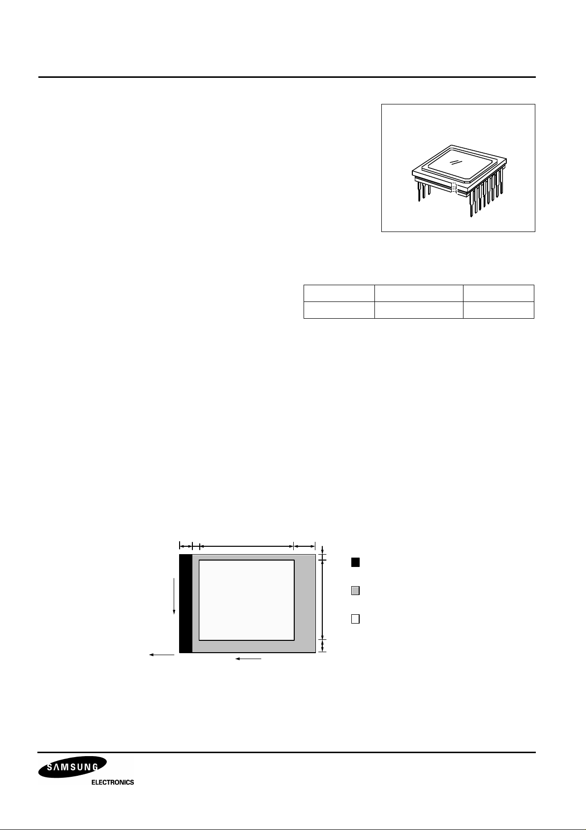
• 16pin Plastic DIP Package
• Field Integration Read Out System
• No DC Bias on Reset Gate
16Pin PLASTIC-DIP
Device Package Operating
KC73129MP 16Pin PLASTIC-DIP -10 °C ~ +55 °C
STRUCTURE
• Number of Total Pixels: 537(H) × 597(V)
• Number of Effective Pixels: 500(H) × 582(V)
• Chip Size: 6.00mm(H) × 5.10mm(V)
• Unit Pixel Size: 9.80µm(H) × 6.30µm(V)
• Optical Blacks & Dummies: Refer to Figure Below
Vertical 1 Line (Even Field Only)
16 7 500 30
1 582 14
V-CCD
OUTPUT
Effective
Imagi ng
Area
Du mmy Pixel s
Optical Black Pixels
E ffective Pixels
1
1/3 INCH CCD IMAGE SENSOR FOR CCIR CAMERA KC73129MP
BLOCK DIAGRAM
(Top View)
8
V
DD
9 10 11 12 13 14 15 16
V
OUT
7 6 5 4 3 2 1
V
GND
V
GG
Φ
L
V
SS
V1
Vertical Shift Register CCD
Vertical Shift Register CCD
Horizontal Shift Register CCD
GND
SUB
VRD
Φ
Φ
V2
RG
Φ
V3
Vertical Shift Register CCD
Φ
H1
Figure 1. Block Diagram
Φ
V4
Vertical Shift Register CCD
Φ
H2
PIN DESCRIPTION
Table 1. Pin Description
Pin Symbol Description Pin Symbol Description
1
2
3
Φ
Φ
Φ
V4
V3
V2
Vertical CCD transfer clock 4 9
Vertical CCD transfer clock 3 10
Vertical CCD transfer clock 2 11
4 SUB Substrate voltage 12 GND Ground
5
6
Φ
V1
V
L
Vertical CCD transfer clock 1 13 VRD Reset drain voltage
Protection bias voltage 14
7 GND Ground 15
8
V
DD
Output AMP drain voltage 16
2
V
V
V
Φ
Φ
Φ
OUT
GG
SS
RG
H1
H2
Signal output
Output AMP gate valtage
Output AMP source valtage
Charge reset clock
Horizontal CCD transfer clock 1
Horizontal CCD transfer clock 2
KC73129MP 1/3 INCH CCD IMAGE SENSOR FOR CCIR CAMERA
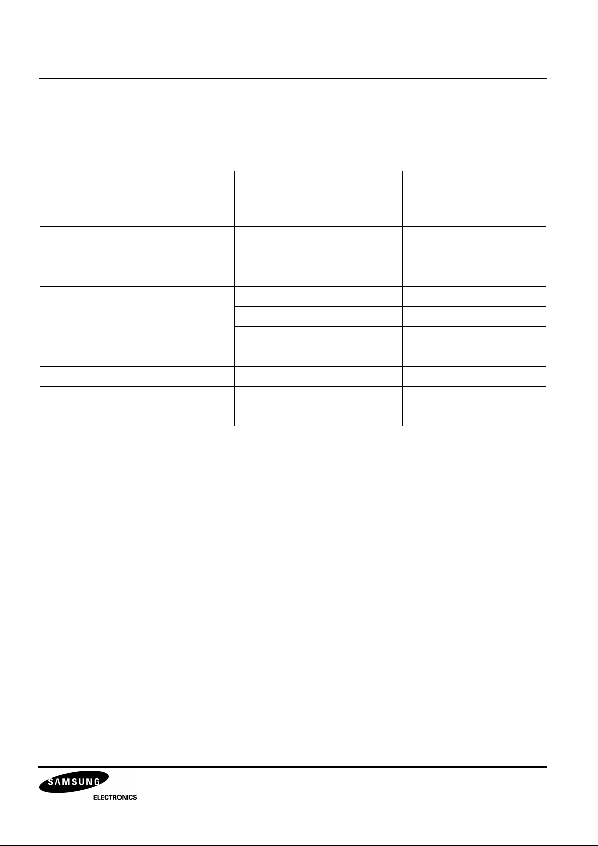
ABSOLUTE MAXIMUM RATINGS
(NOTE)
Table 2. Absolute Maximum Ratings
Characteristics Symbols Min. Max. Unit
Substrate voltage SUB - GND -0.3 55 V
Supply voltage
VDD, V
OUT, VOUT
Vertical clock input voltage ΦV1, ΦV2, ΦV3, Φ
ΦV1, ΦV2, ΦV3, Φ
Horizontal clock input voltage
Voltage difference between vertical and
horizontal clock input pins
ΦH1, ΦH2 - GND
ΦV1, ΦV2, ΦV3, Φ
ΦH1, Φ
H2
ΦH1, ΦH2 - Φ
Output clock input voltage
Protection circuit bias voltage
Operating temperature
Φ
RG, ΦGG
VL - SUB
T
OPR
- GND
V4
- GND
- GND
V4
- V
V4
V4
-0.3 17 V
-10 20 V
L
-0.3 30 V
-0.3 17 V
-0.3 15 V
-0.3 17 V
-17 17 V
-0.3 15 V
-65 0.3 V
-10 55 °C
Storage temperature
NOTE: The device can be destroyed, if the applied voltage or temperature is higher than the absolute maximum rating voltage
or temperature.
T
STG
-30 80 °C
3
1/3 INCH CCD IMAGE SENSOR FOR CCIR CAMERA KC73129MP
DC CHARACTERISTICS
Table 3. DC Characteristics
Item Symbol Min. Typ. Max. Unit Remark
Output amp drain voltage
Output amp gate voltage
Output amp source voltage
V
DD
V
GG
V
SS
14.55 15.0 15.45 V
1.75 2.0 2.25 V
Ground through 680Ω V ±5%
Substrate voltage adjustment range SUB 7.0 14.5 V
Fluctuation range after substrate
voltage adjusted
Protection circuit bias voltage
Output stage drain current
∆V
V
I
SUB
L
DD
-3 3 %
V
voltage of the vertical clock waveform
VL
2.5 mA
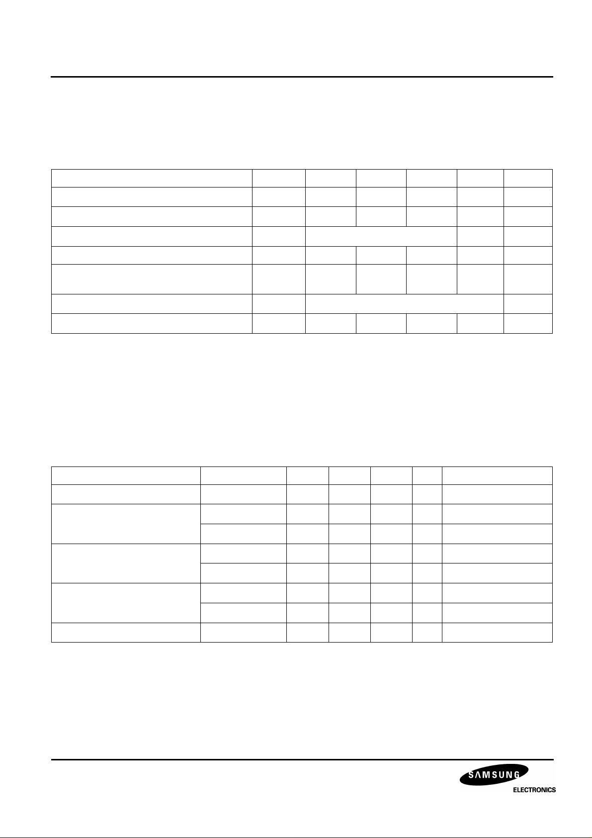
CLOCK VOLTAGE CONDITIONS
Table 4. Clock Voltage Conditions
Item Symbol Min. Typ. Max. Unit Remark
Read-out clock voltage
Vertical transfer clock voltage
Horizontal transfer clock voltage
Charge reset clock voltage
Substrate clock voltage
V
VT
V
~ V
VH1
V
~ V
VL1
V
ΦH
V
HL
V
ΦRG
V
RGLH - VRGLL
V
ΦSUB
VH4
VL4
14.55 15.0 15.45 V High level
-0.05 0.0 0.05 V
-9.5 -9.0 -8.5 V
VVH = (V
VVL = (V
VH1
VL3
+ V
+ V
4.75 5.0 5.25 V High
-0.05 0.0 0.05 V Low
4.75 5.0 5.25 V High
0.8 V Low
20.0 23.0 25.0 V Shutter
VH2
VL4
)/2
)/2
4
KC73129MP 1/3 INCH CCD IMAGE SENSOR FOR CCIR CAMERA
V
=
V
-0.3V
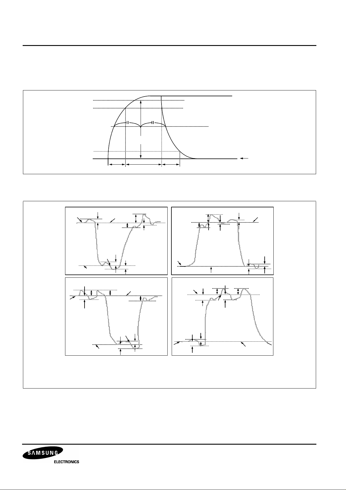
DRIVE CLOCK WAVEFORM CONDITIONS
Read Out Clock Waveform
100%
90%
V
VH1,VVH3
10%
0%
Vertical Transfer Clock Waveform
tr twh tf
0V
¥Õ
V V H 1
¥Õ
V VH2
V 1
V 2
V V H H
V V L 1
V VL
V V HH V VHH
V
VHL
V
VL
V
VH
V V H H
V V H L
V
VL H
V
V
V
V VL H
V VL 2
V VL L
VVH= (V
VV L = (V V L 3 + VV L 4)/ 2
V¥ÕV= V
¥Õ
V 3
V
V H L
V V HL
V VHH
V V HL
V
VH3
V VL 3
VL L
¥Õ
V 4
VH
VHL
V
V
V VL
VH
V VH H
VHL
V V H4
V
VH H
V
VH
V VL H
V
VL L
V
VH H
V
VHL
V VL H
V
VL L
V
VH 1
+ V
VH 2
VL 4
)/2
V
VH H
= VVH+ 0.3V
V
VL
VVH L = VV H - 0. 3 V
VH n
- V
VL n (n = 1~4)
V
= V
V L
V L
+ 0.3V
VL H
VL L
5
1/3 INCH CCD IMAGE SENSOR FOR CCIR CAMERA KC73129MP
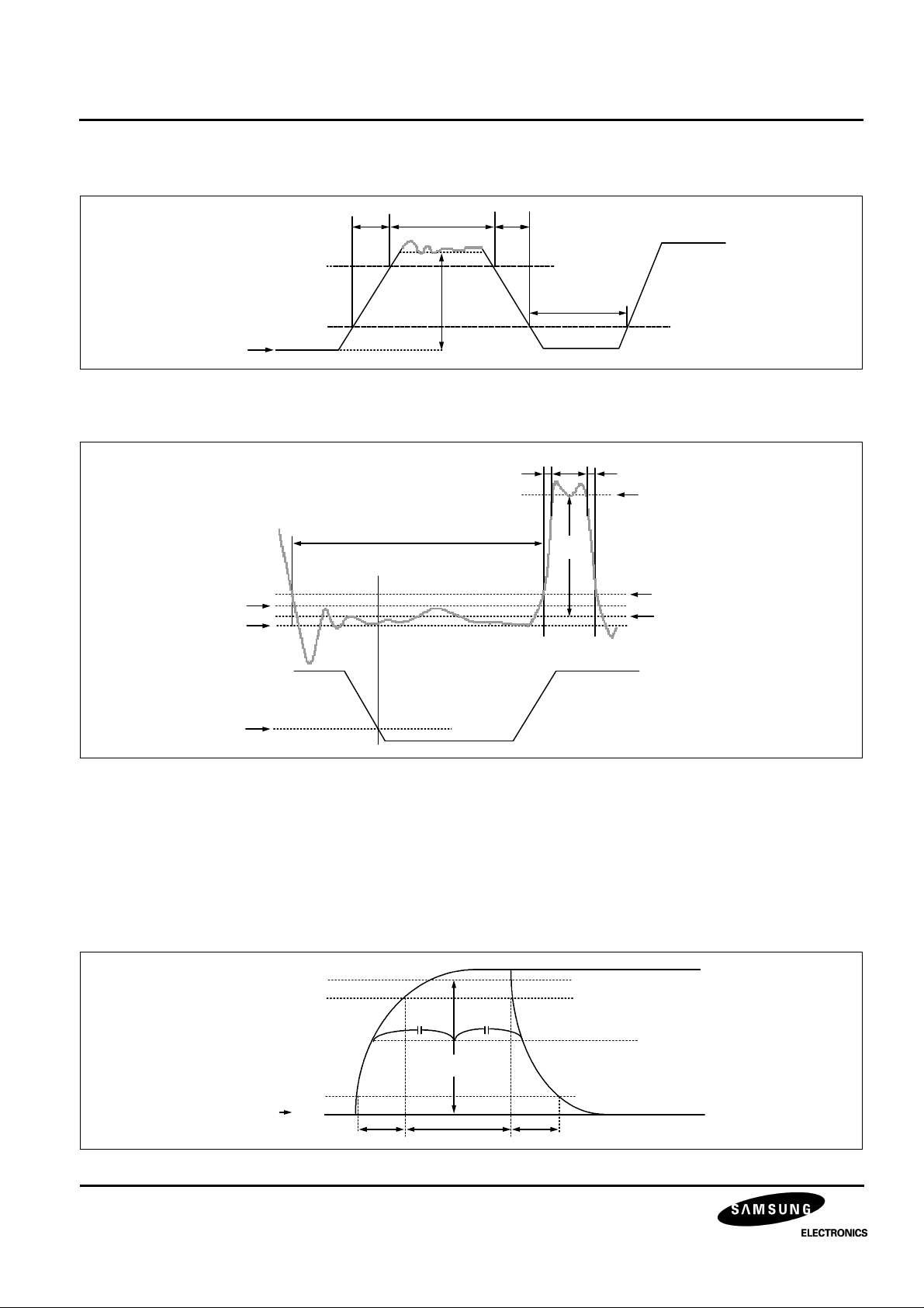
V
Horizontal Transfer Clock Waveform Diagram
90%
10%
HL
Reset Gate Clock Waveform Diagram
RG waveform
V
RGLH
V
RGLL
tr twh
twl
Point A
V¥Õ
tf
H
twl
twh tftr
V
RGH
V
¥Õ
RG
V
+ 0.5V
RGL
V
RGL
¥Õ
H1 waveform
10%
V
is the maximum value and V
RGLH
the diagram about to RG rise
V
RGL
= (V
RGLH
+ V
RGLL
)/2, V
Substrate Clock Waveform
V
SU B
FRG
100%
90%
10%
0%
the minimum value of the coupling waveform in the period from Point A in
RGLL
= V
RGH
- V
RGL
¥Õ
V
SU B
twhtr tf
6
 Loading...