

Samsung KC73125UCA Datasheet
KC73125UCA 1/3 INCH CCD IMAGE SENSOR FOR NTSC CAMERA
ORDERING INFORMATION
H-CCD
INTRODUCTION
The KC73125UCA is an interline transfer CCD area image
sensor developed for NTSC 1/3 inch optical format video
cameras, surveillance cameras, object detectors and image
pattern recognizers. High sensitivity is achieved through the
adoption of Ye, Cy, Mg and G complementary color mosaic
filters, on-chip micro lenses and HAD (Hole Accumulated
Diode) photosensors. This chip features a field integration
read out system and an electronic shutter with variable charge
storage time.
FEATURES
• High Sensitivity
• Optical Size 1/3 inch Format
• Ye, Cy, Mg, G On-chip Comple-mentary Color
Mosaic Filter
• Variable Speed Electronic Shutter
(1/60, 1/100 ~ 1/10,000sec)
• Low Dark Current
• Horizontal Register 5V Drive
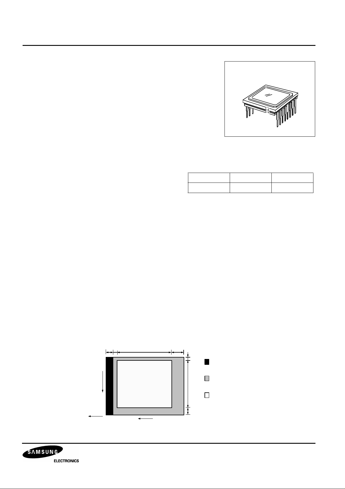
• 16pin Ceramic DIP Package
• Field Integration Read Out System
• No DC Bias on Reset Gate
16Pin Cer DIP
Device Package Operating
KC73125UCA 16Pin Cer DIP -10 °C ~ +60 °C
STRUCTURE
• Number of Total Pixels: 537(H) × 505(V)
• Number of Effective Pixels: 510(H) × 492(V)
• Chip Size: 6.00mm(H) × 4.95mm(V)
• Unit Pixel Size: 9.60µm(H) × 7.50µm(V)
• Optical Blacks & Dummies: Refer to Figure Below
Vertical 1 Line (Even Field Only)
16 2 51 0 25
1 492 12
V-CCD
OUTPU T
E ffective
Imag ing
A rea
Du mmy P ixe l s
Optical Black Pixels
E ffective Pixels
1
1/3 INCH CCD IMAGE SENSOR FOR NTSC CAMERA KC73125UCA
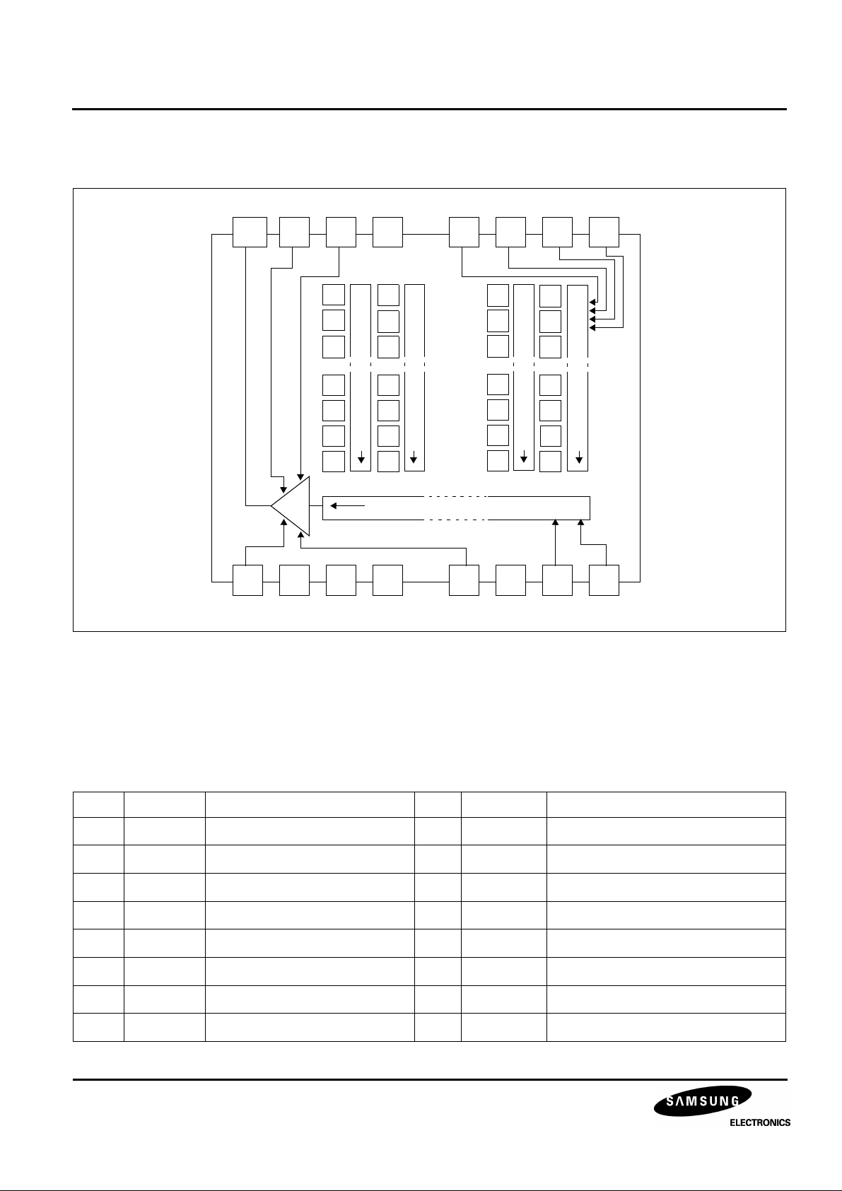
BLOCK DIAGRAM
(Top View)
8
V
OUT
9 10 11 12 13 14 15 16
V
DD
7 6 5 4 3 2 1
V
GND
SS
V
Cy
Mg
Cy
Cy
G
Cy
Mg
GG
GND
Vertical Shift Register CCD
Ye
G
Ye
Ye
Mg
Ye
G
Horizontal Shift Register CCD
V
L
Φ
V1
Vertical Shift Register CCD
Φ
RSSUB
Cy
Mg
Cy
Cy
G
Cy
Mg
Φ
NC
V2
Φ
V3
Vertical Shift Register CCD
Ye
G
Ye
Ye
Mg
Ye
G
Φ
H1
Vertical Shift Register CCD
Φ
Φ
V4
H2
Figure 1. Block Diagram
PIN DESCRIPTION
Table 1. Pin Description
Pin Symbol Description Pin Symbol Description
1
2
3
4
Φ
Φ
Φ
Φ
V4
V3
V2
V1
Vertical CCD transfer clock 4 9
Vertical CCD transfer clock 3 10 GND Ground
Vertical CCD transfer clock 2 11 SUB Substrate bias
Vertical CCD transfer clock 1 12
5 GND Ground 13
V
V
V
OUT
GG
SS
Output stage gate bias 14 NC No connection
Output stage source bias 15
Signal output 16
6
7
8
V
Φ
Φ
Φ
V
DD
RS
H1
H2
Output stage drain bias
L
Protection circuit bias
Charge reset clock
Horizontal CCD transfer clock 1
Horizontal CCD transfer clock 2
2
KC73125UCA 1/3 INCH CCD IMAGE SENSOR FOR NTSC CAMERA
ABSOLUTE MAXIMUM RATINGS
(NOTE)
Table 2. Absolute Maximum Ratings
Characteristics Symbols Min. Max. Unit
Substrate voltage SUB - GND -0.3 55 V
Supply voltage VDD, V
VDD, V
Vertical clock input voltage ΦV1,ΦV2, ΦV3, Φ
ΦV1, ΦV2, ΦV3, Φ
ΦV1, ΦV2, ΦV3, Φ
Horizontal clock input voltage ΦH1, ΦH2 - GND
ΦH1, ΦH2 - SUB
Voltage difference between vertical and
ΦV1, ΦV2, ΦV3, Φ
horizontal clock input pins
ΦH1, Φ
OUT
OUT
H2
, V
, V
SS
SS
- GND
- SUB
- GND
V4
- V
V4
- SUB
V4
V4
-0.3 18 V
-55 10 V
-10 20 V
L
-0.3 30 V
-55 10 V
-0.3 10 V
-55 17 V
15 V
27
17 V
V
ΦH1, ΦH2 - Φ
V4
Output clock input voltage ΦRS, VGG - GND
ΦRS, VGG - SUB
Protection circuit bias voltage
Operating temperature
Storage temperature
NOTE: The device can be destroyed, if the applied voltage or temperature is higher than the absolute maximum rating voltage
or temperature.
VL - SUB
T
OP
T
STG
-17 17 V
-0.3 15 V
-55 10 V
-55 10 V
-10 60 °C
-30 80 °C
3
1/3 INCH CCD IMAGE SENSOR FOR NTSC CAMERA KC73125UCA
DC CHARACTERISTICS
Table 3. DC Characteristics
Item Symbol Min. Typ. Max. Unit Remark
Output stage drain bias
Output stage gate voltage
Output stage source voltage
Substrate voltage adjustment range
Fluctuation voltage range after substrate
voltage adjusted
Protection circuit bias voltage
Output stage drain current
CLOCK VOLTAGE CONDITIONS
Table 4. Clock Voltage Conditions
Item Symbol Min. Typ. Max. Unit Remark
V
∆V
V
V
V
I
DD
GG
SS
SUB
SUB
V
L
DD
14.55 15.0 15.45 V
1.75 2.0 2.25 V
Ground through 680Ω V ±5%
7.0 14.5 V
-3 3 %
The lowest vertical clock level
2.5 mA
Read-out clock voltage
Vertical transfer clock voltage V
Horizontal transfer clock voltage V
V
VM1
V
V
VH1
VL1
HH1
HL1
Charge reset clock voltage V
Substrate clock voltage
V
, V
~ V
~ V
, V
, V
RSH
V
RSL
ΦSUB
VH3
VM4
VL4
HH2
HL2
14.55 15.0 15.45 V High level
-0.2 0.0 0.2 V Middle
-9.5 -9.0 -8.5 V Low
4.75 5.0 5.25 V High
-0.2 0.0 0.2 V Low
4.75 5.0 5.25 V High
-0.2 0.0 0.2 V Low
20 23.0 25 V Shutter
4
KC73125UCA 1/3 INCH CCD IMAGE SENSOR FOR NTSC CAMERA
V
=
V
-0.3V
DRIVE CLOCK WAVEFORM CONDITIONS
Read Out Clock Waveform
100%
90%
V
VH1,VVH3
10%
0%
Vertical Transfer Clock Waveform
tr twh tf
0V
¥Õ
V V H 1
¥Õ
V VH2
V 1
V 2
V V H H
V V L 1
V VL
V V HH V VHH
V
VHL
V
VL
V
VH
V V H H
V V H L
V
VL H
V
V
V
V VL H
V VL 2
V VL L
VVH= (V
VV L = (VV L 3 + V V L 4) / 2
V¥ÕV= V
¥Õ
V 3
V
V H L
V V HL
V VHH
V V HL
V
VH3
V VL 3
VL L
¥Õ
V 4
V
VH
VHL
VH
V
V VL
V VH H
VHL
V V H4
V
VH H
V
VH
V VL H
V
VL L
V
VH H
V
VHL
V VL H
V
VL L
V
VH 1
+ V
VH 2
VL 4
)/2
V
VH H
= VVH+ 0. 3V
V
VL
VVH L = VV H - 0. 3 V
VH n
- V
VL n (n = 1 ~4)
V
= V
V L
V L
+ 0. 3V
VL H
VL L
5
1/3 INCH CCD IMAGE SENSOR FOR NTSC CAMERA KC73125UCA
V
Horizontal Transfer Clock Waveform Diagram
90%
10%
HL
Reset Gate Clock Waveform Diagram
RG waveform
V
RGLH
V
RGLL
tr twh
twl
Point A
V¥Õ
tf
H
twl
twh t ftr
V
RGH
V
¥Õ
RG
V
+ 0.5V
RGL
V
RGL
¥Õ
H1 waveform
10%
V
is the maximum value and V
RGLH
the diagram about to RG rise
V
RGL
= (V
RGLH
+ V
RGLL
)/2, V
Substrate Clock Waveform
V
SU B
FRG
100%
90%
10%
0%
the minimum value of the coupling waveform in the period from Point A in
RGLL
= V
RGH
- V
RGL
¥Õ
V
SU B
twhtr tf
6
 Loading...