

Samsung KB8823, KB8822, KB8821 Datasheet
PRELIMINARY SPECIFICATION (V1.5)
FREQUENCY SYNTHESIZER
INTRODUCTION
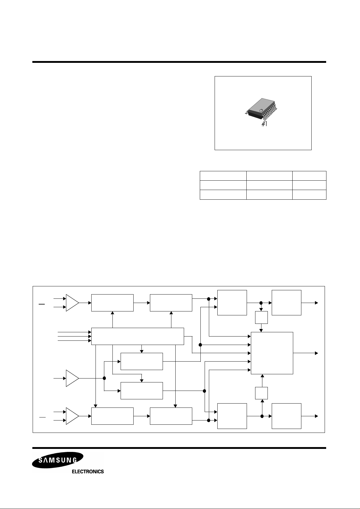
The KB8821/22/23 are high performance dual frequency synthesizers with integrated prescalers designed for RF operation
up to 1.2GHz/2.0GHz/2.5GHz and IF operation up to 520MHz.
The KB8821/22/23 contain dual-modulus prescalers. The RF
synthesizer adopts a 64/65 or an 128/129 prescaler(32/33 or
64/65 for the KB8823) and the IF synthesizer adopts an 8/9 or
a 16/17 prescaler.
Using a proprietary digital phase-locked-loop technique, the
KB8821/22/23 have linear phase detector characteristic and
can be used for very stable, low noise local oscillator signal.
Supply voltage can range from 2.7V to 4.0V. The KB8821/22/
23 are now available in a 20-TSSOP/24-QFN package.
FEATURES
• Very low current consumption(8821:3.5mA, 22:4.5mA, 23:5.5mA)
• Operating voltage range : 2.7 ~ 4.0V
• Selectable power saving mode(Icc=1uA typical @3V)
• Dual modulus prescaler :
KB8821/22 (RF) 64/65 or 128/129
KB8823 (RF) 32/33 or 64/65
KB8821/22/23 (IF) 8/9 or 16/17
• Programmability via serial bus interface
• No dead-zone PFD
• Variable charge pump output current
• High speed lock mode
KB8821/22/23
20-TSSOP-225
ORDERING INFORMATION
Device Package Tem. Range
KB8821/22/23 20-TSSOP-225 -40 ~ +85°C
KB8821/22/23 24-QFN* -40 ~ +85°C
* QFN : Quad Flat Non-leaded(see Addendum).
APPLICATIONS
• Cellular telephone systems : KB8821
• Portable wireless communications : KB8822
(PCS/PCN, cordless)
• Wireless Local Area Networks (W-LANs)
: KB8823
• Other wireless communication systems
BLOCK DIAGRAM
finRF
finRF
CLOCK
LE
DATA
OSCin
finIF
finIF
+
-
+
-
RF
Prescaler
Serial Data Control
IF
Prescaler
RF
N Counter
RF
R Counter
IF
R Counter
IF
N Counter
Figure 1. BLOCK DIAGRAM
RF
Phase
Detector
IF
Phase
Detector
Charge
Pump
RF
LD
foLD
Data Out
Multiplexer
IF
LD
IF
Charge
Pump
RF
CPoRF
foLD
CPoIF
199-06-15
PRELIMINARY SPECIFICATION (V1.5)
CLOCK
FREQUENCY SYNTHESIZER
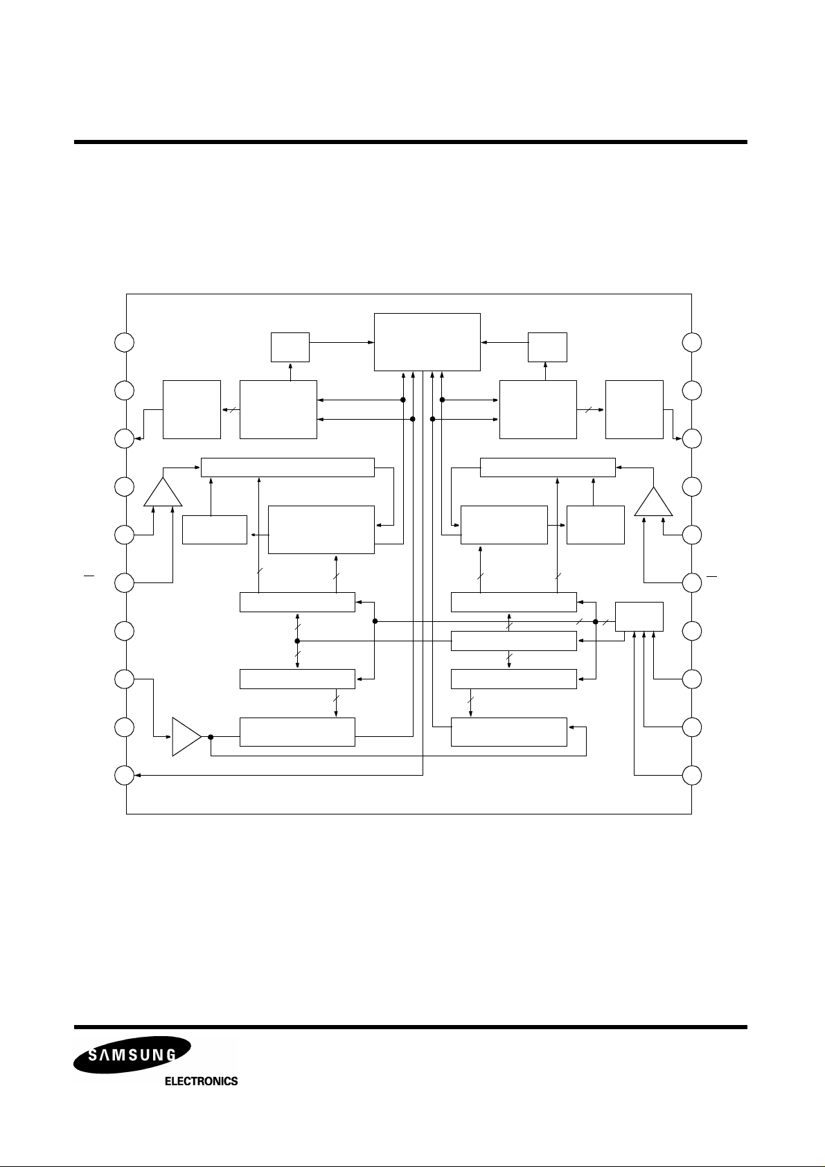
BLOCK DIAGRAM- Continued
KB8821/22/23
VDD1
VP1
CPoRF
GND
finRF
finRF
GND
OSCin
GND
1
2
3
4
5
6
7
8
9
RF
Charge
Pump
+ –
Prescaler
Control
RF
LD
RF
Phase
Detector
RF Prescaler
RF
Programmable
Counter
RF N-Latch
RF R-Latch
RF Reference
Counter
foLD
Data Out
Multiplexer
IF
LD
IF
Phase
Detector
IF Prescaler
IF
Programmable
Counter
IF N-Latch
20-bit Shift Register
IF R-Latch
IF Reference
Counter
Prescaler
Control
IF
Charge
Pump
– +
2-bit
Control
20
19
18
17
16
15
14
13
12
VDD2
VP2
CPoIF
GND
finIF
finIF
GND
LE
DATA
foLD
10
11
Figure 2. Detailed block diagram
299-06-15
PRELIMINARY SPECIFICATION (V1.5)
FREQUENCY SYNTHESIZER
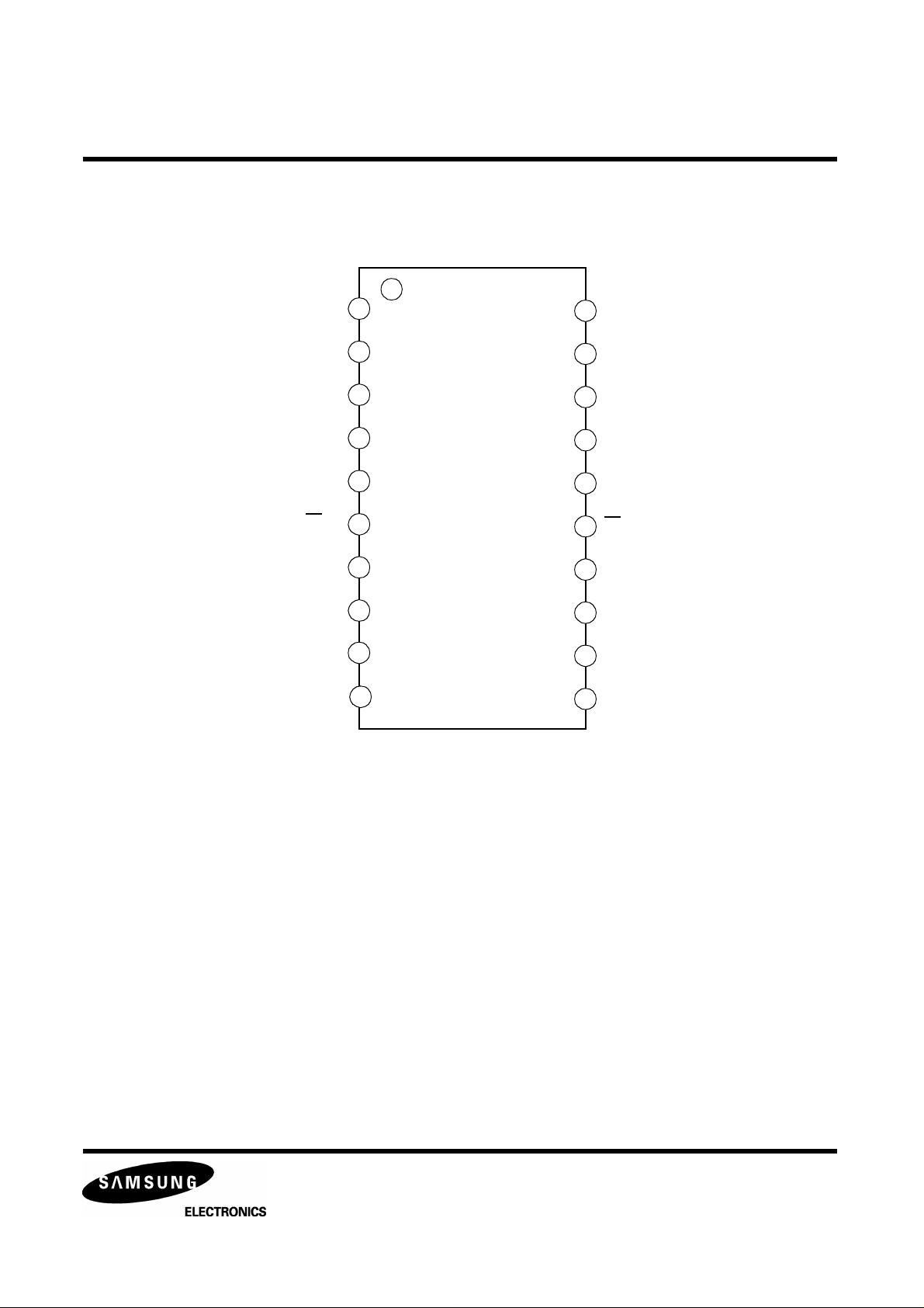
PIN CONFIGURATION
VDD1
1
Vp1
2
20
19
KB8821/22/23
VDD2
Vp2
CPoRF
(Digital)
finRF
finRF
GND
3
4
KB8821
5
KB8822
6
18
17
(Digital)
16
15
KB8823
GND
GND
foLD
7
Top View
8
9
10
20-TSSOP
(Analog)
OSCin
(Digital)
20-Lead(0.173 Wide) Thin Shrink Small
Outline Package(20-TSSOP)
14
(Analog)
13
12
11
CPoIF
GND
finIF
finIF
GND
LE
DATA
CLOCK
1. pin #9 = pin #17(internally connected).
2. Do not tie up Vp and VDD
: Vp is the source of digital noises. The power
for analog part is supplied by VDD. If Vp and
VDD are tied together, noisy Vp corrupts the
power source for the analog part.
399-06-15
PRELIMINARY SPECIFICATION (V1.5)
FREQUENCY SYNTHESIZER
KB8821/22/23
PIN DESCRIPTION
Pin No Symbol I / O Description
1 VDD1 - Power supply voltage input for the RF PLL part. VDD1 must equal VDD2. In
order to reject supply noise, bypass capacitors must be placed as close as
possible to this pin and be connected directly to the ground plane.
2 Vp1 - Power supply voltage input for RF charge pump( ≥ VDD1).
3 CPoRF O Internal RF charge pump output for connection to an external loop filter whose
filtered output drives an external VCO.
4 GND - Ground for RF digital blocks.
5 finRF I RF prescaler input. The signal comes from the external VCO.
6 finRF I The complementary input of the RF prescaler. A bypass capacitor must be
placed as close as possible to this pin and be connected directly to the ground
plane. The bypass capacitor is optional with some loss of sensitivity.
7 GND - Ground for RF analog blocks.
8 OSCin I Reference counter input. TCXO is connected via a coupling capacitor.
9 GND - Ground for IF digital blocks.
10
11 CLOCK I CMOS clock input. Serial data for the various counters is transfered into the
12 DATA I Binary serial data input. The MSB of CMOS input data is entered first. The
13 LE I Load enable CMOS input. When LE becomes high, the data in the shift
14 GND - Ground for IF analog blocks.
15 finIF I The complementary input of the IF prescaler. A bypass capacitor must be
16 finIF I IF prescaler input. The signal comes from the external VCO.
17 GND - Ground for IF digital blocks.
18 CPoIF O Internal IF charge pump output for connection to an external loop filter whose
foLD
O Multiplexed output of the RF/IF programmable counters, the reference
counters, the lock detect signals and the shift registers. The output level is
CMOS level. (see fout Programmable Truth Table)
22-bit shift register on the rising edge of the clock signal.
control bits are on the last two bits. CMOS input.
register is loaded into one of the four latches(by the control bits).
placed as close as possible to this pin and be connected directly to the ground
plane. The bypass capacitor is optional with some loss of sensitivity.
filtered output drives an external VCO.
19 Vp2 - Power supply voltage input for IF charge pump( ≥ VDD2)
20 VDD2 - Power supply voltage input for the IF PLL part. VDD1 must equal VDD2. In
order to reject supply noise, bypass capacitors must be placed as close as
possible to this pin and be connected directly to the ground plane.
499-06-15
PRELIMINARY SPECIFICATION (V1.5)
FREQUENCY SYNTHESIZER
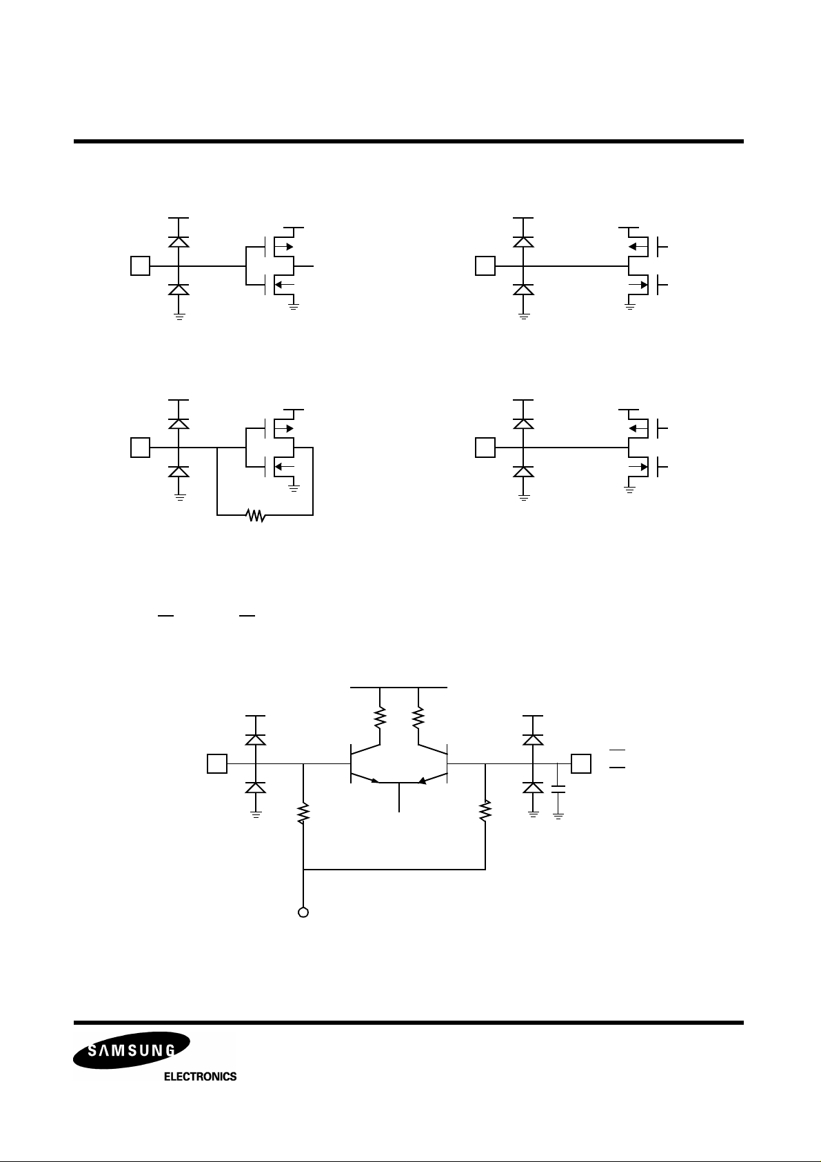
EQUIVALENT CIRCUIT DIAGRAM
♦ CLOCK, DATA, LE ♦ foLD
♦ OSCin ♦ CPoRF, CPoIF
KB8821/22/23
♦ finRF, finRF, finIF, finIF
finRF,
finIF
finRF,
finIF
Vbias
599-06-15
PRELIMINARY SPECIFICATION (V1.5)
FREQUENCY SYNTHESIZER
ABSOLUTE MAXIMUM RATINGS
Characteristic Symbol Value Unit
KB8821/22/23
Power Supply Voltage V
Power Dissipation P
Operating Temperature T
Storage Temperature T
DD
D
a
STG
5.5 V
600 mW
-40°C ~ +85oC
-65°C ~ +150oC
°C
°C
ELECTROSTATIC CHARACTERISTICS
Characteristic Pin No. ESD level Unit
Human Body Model All < ±2000 V
Machine Model All < ±300 V
Charged Device Model All < ±800 V
** These devices are ESD sensitive. These devices must be handled in the ESD protected environment.
699-06-15
PRELIMINARY SPECIFICATION (V1.5)
FREQUENCY SYNTHESIZER
KB8821/22/23
ELECTRICAL CHARACTERISTICS (V
Characteristic Symbol Test Conditions Min. Typ. Max. Unit
V
Power Supply Voltage
KB8823 RF + IF
KB8823 RF Only 4.0
Power Supply
Current
KB8822 RF + IF 4.5
KB8822 RF Only 3.0
KB8821 RF + IF 3.5
KB8821 RF Only 2.0
KB882x IF Only 1.5
Power down Current I
Digital inputs : CLOCK, DATA and LE
High-Level Input Voltage V
DD
V
P
I
DD
PWDN
IH
=3.0V, VP=3.0V, -40οC≤Ta≤85οC Unless otherwise specified)
DD
2.7 3.0 4.0
V
DD
3.0 4.0
5.5
VDD=2.7V to 4.0V
VDD=3.0V 1.0 10 µA
VDD=2.7V to 4.0V 0.7V
DD
V
mA
V
Low-Level Input Voltage V
High-Level Input Current I
Low-Level Input Current I
Reference Divider Input : OSCin
Input Current
Digital Output : foLD
High Level Output Voltage V
Low Level Output Voltage V
I
IHR
I
IH
IL
ILR
OH
OL
VDD=2.7V to 4.0V 0.3V
IL
DD
V
VIH= VDD=4.0V -1.0 +1.0 µA
VIL=0V, VDD=4.0V -1.0 +1.0 µA
VIH= VDD=4.0V +100 µA
VIL=0V, VDD=4.0V -100 µA
Iout = -500µA
VDD-0.4
V
Iout = +500µA 0.4 V
799-06-15
 Loading...