

Samsung KB8527BQ Datasheet
KB8527B 1 CHIP CLP SUBSYSTEM IC
INTRODUCTION
KB8527B is a monolithic circuit which can be used in high
performance 60MHz MCA type CLP System.
The KB8527B is a subsystem IC for FM / FSK receiving systems and a complete one chip FM / FSK receiver IC for 60MHz
system. It`s feature includes receiving functions for FM / FSK
systems, a compandor to remove external noise, and PLL ( Phase Lock Loop ) of channel selection which blocks surrounding
frequency interference.
The KB8527B can be used with a wide range of FM / FSK VHF
bandwidth systems, including cordless phone, and the narrow
band voice and data sending / receiving systems.
To make applications easily and simply, pheripheral parts are
minimized.
ORDERING INFORMATION
Device Package Operating Temperature
48 -QFP- 1010E
+ : New product
FEATURES
¡Ü Operating voltage range : 2.0V ~ 5.5V
¡Ü Typical supply current : 13.5mA at 3.6V
¡Ü Built - in low battery detection function ( selectable 3.45V, 3.3V, 3.0V, 2.2V, 2.1V )
¡Ü Built - in speaker amplifier
• Built - in splatter filter
• Built - in dual conversion receiver, compandor and universal PLL
¡Ü FM Receiver
- Complete dual coversion circuit
- Excellent input sensitivity (0.7µVrms at 20dB SINAD)
¡Ü Compandor
- Easy gain control to use external component
- Included ALC (Automatic Level Control) circuit
- Included Mute logic
¡Ü Universal PLL
- RX (TX) divided counter range : 1/16 ~ 1/16383
- Reference frequency divided counter range : 1/16 ~ 1/4095
- Lock detector signal output
- Serial interface with MICOM for controlling each block
-20oC ~ + 70oC+ KB8527BQ 48 - QFP - 1010E
KB8527B 1 CHIP CLP SUBSYSTEM IC
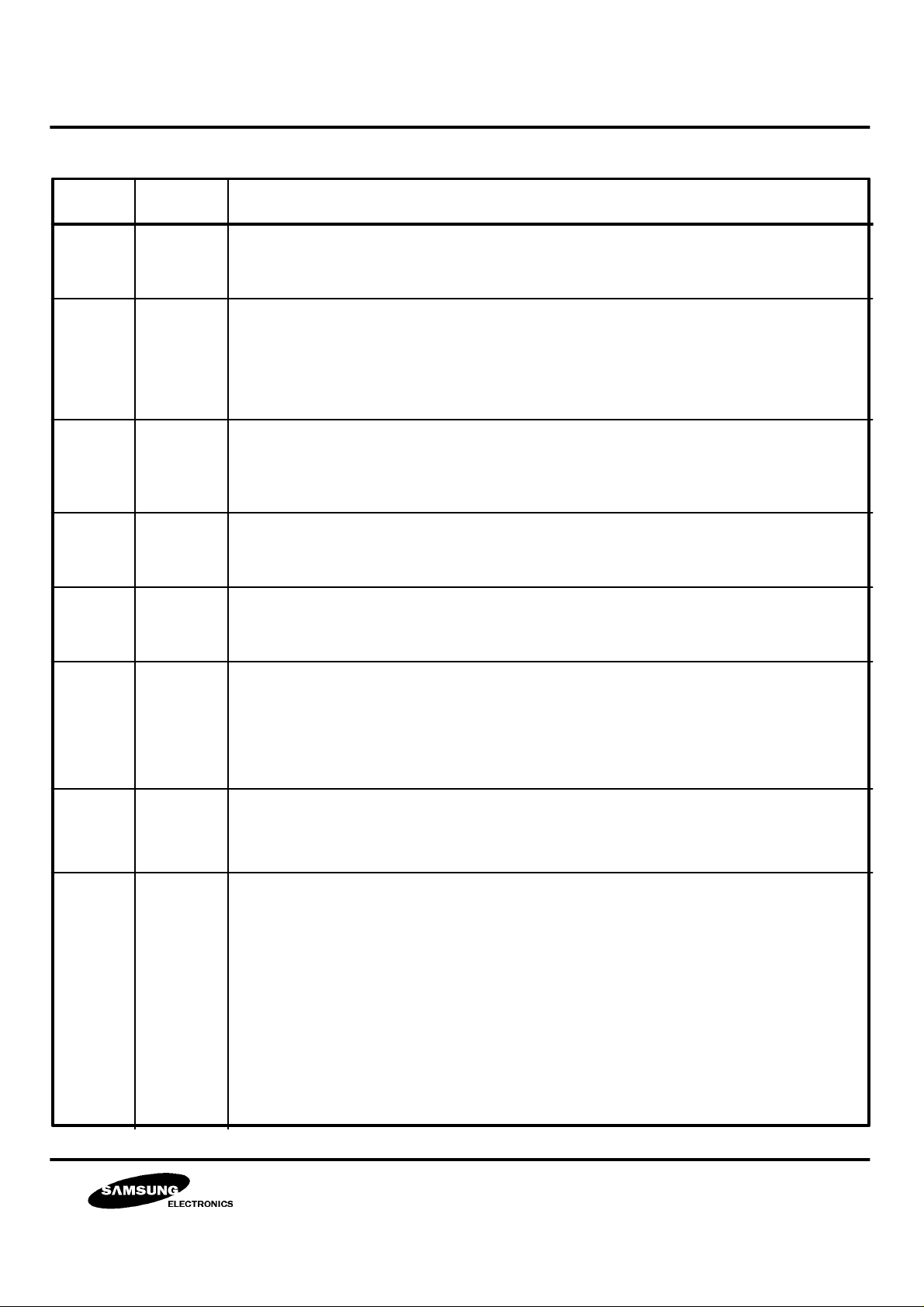
BLOCK DIAGRAM
2MI
1MO
1LOI
1LOI
VCO
RX
1MI
1MI
GND
(PLL)
PDR
V
REF
(PLL)
V
(PLL)
TIF
LD
(RX)
GND
30
Meter
Driver
Carrier
Detector
Low
Battery
Detector
QCI
RAO
29 28 27
Limiter
Gain Cell
Rectifier
DSCI
FSK
COMP
DSCO
26
Rectifier
Gain Cell
25
SUM
AMP
MDO
Regulator
(1V)
PRI
+
-
SUM
AMP
SPK
AMP
SPK
AMP
+
-
PRI
ALC
VREF
V
REF
24
(COMP)
23
ALC
22
EPI
21
ERC
EO
20
SAI
19
SAO1
18
SAO2
17
VCC
16
(COMP)
GND
15
(COMP)
CPI+
14
13
CPI -
(RX)
VCC
LI
32 31
Limiting
IF AMP
37
2LOI
36
X-tal
OSC
2`nd
MIX
35
2LOI
2MO
34 33
IF AMP
(455KHz)
38
39
40
RX
VCO
Quad
Detector
AMP
41
42
1`st
MIX
IF AMP
(10.7MHz)
Regulator
43
44
( 2.15 V )
Buffer
Programmable Counter
45
46
CC
47
48
( RX )
Programmable Counter
( TX )
Programmable Counter
( REF )
4_25 CNT
RX Phase
Detector
TX Phase
Detector
CO
PDT
SFI
Splatter
Filter
SFO
fMCU
CDO/LDT
CONTROL
6
(PLL)
GND
CLK
DATA
EN
LBD
AGIC
Compandor
mute
121110 9 8 754 3 1 2
CRC
KB8527B 1 CHIP CLP SUBSYSTEM IC
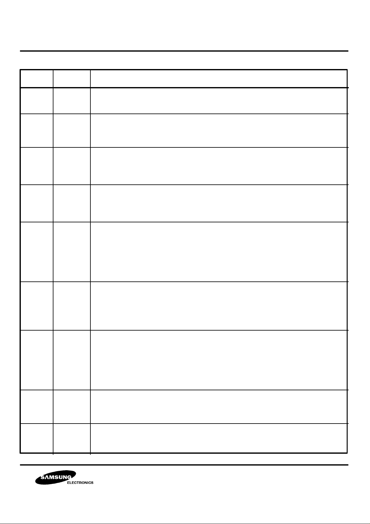
PIN CONFIGURATION
VCO
GND
V
REF(PLL)
V
CC(PLL)
2MI
1MO
1LOI
1LOI
RX
1MI
1MI
(PLL)
PDR
37
38
39
40
41
42
43
44
45
46
47
36
2LOI
35
2LOI
34 33
2MO
LD
(RX)
GND
30
(RX)
VCC
LI
32 31
KB8527B
29
QCI
RAO
28
27
DSCI
26
DSCO
MDO
25
24
23
22
21
20
19
18
17
16
15
14
V
REF(COMP)
ALC
EPI
ERC
EO
SAI
SAO1
SAO2
VCC
(COMP)
GND
(COMP)
CPI+
TIF
48
1
PDT
2
CO
3
SFI
4 5 6
SFO
CDO/LDT
(PLL)
GND
7
CLK
8
DATA
9
EN
10 11
LBD
12
AGIC
13
CRC
CPI -
KB8527B 1 CHIP CLP SUBSYSTEM IC
PIN DESCRIPTION
Pin No Symbol Description
Phase detector output terminal of the transmitter at PLL.
1
PDT
If fTX > f
If fTX < f
if fTX = f
or fTX is leading the output is negative pulse
REF
or fTX is lagging the output is positive Pulse
REF
and the same phase the output is High Impedance
REF
2
CO
Compressor output terminal of compandor ; connected to the splatter filter amp
input terminal.
3
4
SFI
SFO Output terminal of Splatter filter amp.
Input terminal of Splatter filter amp.
LDT : Output terminal of transmitter lock detector in PLL block. Output is low
if PLL is in lock state and is high if PLL is in unlock state.
5
LDT/
CDO
CDO : As an output terminal of the carrier detector buffer, connected to (RSSI )
terminal of MICOM. This pin outputs the contents of Meter Driver buffer
which is turned on / off, according to the signal level detected by Meter
Driver.
Ground.
6
GND
PLL
Ground of logic section at PLL.
CLK7
8
9
10
DATA
EN
LBD
11 AGIC
These pins are serial interface terminals for programming reference counter,
auxiliary reference counter, TX channel counter, RX channel counter and control
block that controls internal each block with test mode and power saving mode.
Low Battery Detecting output. ( Selectable 3.45V, 3.3V, 3.0V, 2.2V, 2.0V ).
During the normal operation, output level is low, but it is high at low battery
detection. As this pin is an open collector type, it requires a pull - up resister.
This pin bypasses AC elements at the feedback loop which come from the SUM
amp block of COMPRESSOR. A capacitor should be connected between this terminal and GND. ( C = 2.2 uF )

KB8527B 1 CHIP CLP SUBSYSTEM IC
Pin No Symbol Description
12 CRC
13
CPI -
14 CPI +
15
16
17
GND
(COMP)
Vcc
(COMP)
SAO 2
Converts waveform from the full wave rectifier to DC element at the rectifier block
of Compressor. ( RC = 33 msec )
Pre - amp inverting input terminal of Compressor.
Adjusts the negative feedback loop gain. ( in application, gain is 5 )
Pre - amp non - inverting input terminal of Compressor.
Used as an input terminal for voice signals.
Ground.
Ground of Compandor.
Supply voltage.
Power supply terminal of Compandor.
Output terminal of speaker amp 2.
This signal is the same as SAO1 output, but phase difference is 180o for SAO1.
DC voltage level is ( Vcc - 0.7V ) / 2.
18 SAO 1
Output terminal of Speaker amp 1.
DC voltage level is ( Vcc - 0.7V ) / 2.
19 SAI
Speaker Amp 1 input terminal.
Between this terminal and Expander output terminal, uses a AC coupled.
20 EO Output terminal of Expander, from which a regenerated voice signals are emitted.
Converts waveform from the full wave rectifier to DC element at the rectifier block
21
22
ERC
EPI -
of Expander. ( RC = 33 msec )
Pre - amp inverting input terminal of Expander.
Adjusts the negative feedback loop gain. ( in application, gain is 5 )
Reference current input terminal of Automatic Level Control ( ALC) ; Adjusts THD
of compressor output voltage to less than 3 % or limites the frequency deviation
23 ALC
of TX if the input is higher than a certain level. The ALC circuit may be turned
off depending on the ALC reference current or the magnitude of output voltage
may be limited if it is higher than a certain level. ( Iref = 8uA, Ralc = 120KΩ )
KB8527B 1 CHIP CLP SUBSYSTEM IC
Pin No Symbol Description
24
25
26
27
V
REF(COMP)
MDO
DSCO
DSCI
28 RAO
29 QCI
Reference voltage ( V
= 1V ). Supplies a regulator voltage to the Compressor and
REF
Expander of COMPANDER.
Output terminal of the Meter Driver.
Amplitude of RF input signal for useful frequency is detected by Meter Driver
circuit. The Meter Driver circuit has perfect linear characteristic of 60 dB range
for input signal level. ( 0.1µV / dB )
Output terminal of Data Slicing comparator.
Seperates Frequency Shift Keying ( FSK ) serial data and executes data shapping
and limiting.
Input terminal of Data slicing comparator.
Non - inverting type with the negative input terminal biased to 1/2 Vcc.
Recovered Audio Output terminal. Voice signals detected by the Quadrature
Detector are amplified and then output through this terminal.
Quadrature coil input terminal.
The 455 KHz oscillator circuit is an Lp=680uH, Cp=180pF valued LC tank circuit.
Voice signals are detected by mixture of 455 KHz ( by phase difference ) which
is converted from mixer 2.
30 GND
31
32
LD
LI
RX
Ground .
Ground for Receiver.
Limiter input and decoupling terminal.
Removes amplitude modulation elements caused by fading or FM signal noise.
Limiting IF amplifies and limits the second intermediate frequency, 455 KHz.
The input impedance of the limiting IF amplifier is set to 1.5 KΩ.
While FM waves are transmitted with constant magnitude, their magnitudes are
slightly modulated due to reflection from obstacles, fading phenomenon, noise
wave, and mixing with AM wave elements before entering the receiver`s antenna.
The limiter makes amplitude uniform by removing these AM wave elements.
KB8527B 1 CHIP CLP SUBSYSTEM IC
Pin No Symbol Description
33 V
CC(RX)
2MO34
2LOI35
2LOI36
37 2MI
38 1MO
Supply voltage.
Supplies power to the Receiver.
Output terminal of Mixer 2. Second intermediate frequency ( 455 KHz ), generated
by mixing first intermediate frequency ( 10.7 MHz ) and Second Local Oscillator is
output.
Input terminal of second local oscillator. Generates second local oscillator
frequency to convert output from mixer 1 ( 10.7 MHz ) into second intermediate
frequency. It is an oscillator with crystal of 10.24 MHz and 10.245 MHz.
Input terminal of mixer 2. Output from mixer 1 is entered to mixer 2 input terminal
via 10.7 MHz ceramic filter. Second mixer converts frequency to second intermediate frequency ( 455 KHz : AM IF ).
Output terminal of mixer 1.
The signal from mixer 1 and the frequency of the first local oscillator are mixed
to produce the first intermediate frequency, which is the output through this
terminal. The output terminal is an emitter follower with an output impedance of
330Ω to match the 330Ω input / output impedance of the 10.7 MHz ceramic filter.
39
40
41
1LOI
1LOI
VCORX
42 1MI
43 1MI
44
GND
(PLL)
Input terminal of the first local oscillator.
The local oscillator is a voltage controlled oscillator. local oscillation frequency
and received frequency are mixed at mixer 1 and then conerted to the first
intermediate frequency of 10.7 MHz or 10.695 MHz.
The terminal which variable capacitor is included in the chip. Used as an input
terminal where 1`st local oscillation frequency is changed by varying the capacitor
connected between 1`st local oscillator terminals.
The internal variable capacitor has the value of 18.73 ~ 15.86 pF depending on the
applied voltage. ( 1.0 ~ 2.0 V )
Input terminal of Mixer 1. This mixer is made of double balanced multiplier.
The received signal amplied at RF AMP is input to this teminal.
Ground.
Ground for analog at PLL.
 Loading...