

Samsung KB2516 Datasheet
TRIPLE 8-BIT ANALOG-TO-DIGITAL CONVERTER KB2516 (Preliminary)
SUMMARY
The KB2516 is a triple 8-bit analog-to-digital converter optimized for digitizing R/G/B graphics signal from PC and
workstation. Its 140MSPS encode rate capability and analog bandwidth of 500MHz supports support display
resolution of up to SXGA (1280 × 1024) class. The IC also includes a PLL (Phase Locked Loop) system that can
be locked on horizontal line frequency, and generates the ADC clock.
FEATURES
• Analog bandwidth of 500MHz
• 3 clamps for 256 programmable levels
• 3 programmable gain amplifiers
• Analog input range: 0.5Vpp to 1.0Vpp
• Triple 8-bit ADC
• Sampling rate up to 140MHz
• Fully integrated PLL to generate the ADC clock,
which can be locked to a HSYNC
ORDERING INFORMATION
Device Package Ordering Information
KB2516 144-LQFP-2020
APPLICATIONS
• Integrated PLL divider
• Programmable clock phase control (Φstep = 7.5°)
Integrated SOG separator and HSYNC input
polarity detector
• Single and double pixel width output data bus
2
• Support I
• Power down mode
• 1.25W power dissipation
C and 3-wire serial interface
• RGB high speed digitizing
• LCD desktop monitor
• Plasma display pannel panel
RELATED PRODUCTS
KS2530 FRC & SCALER
1
KB2516 (Preliminary) TRIPLE 8-BIT ANALOG-TO-DIGITAL CONVERTER
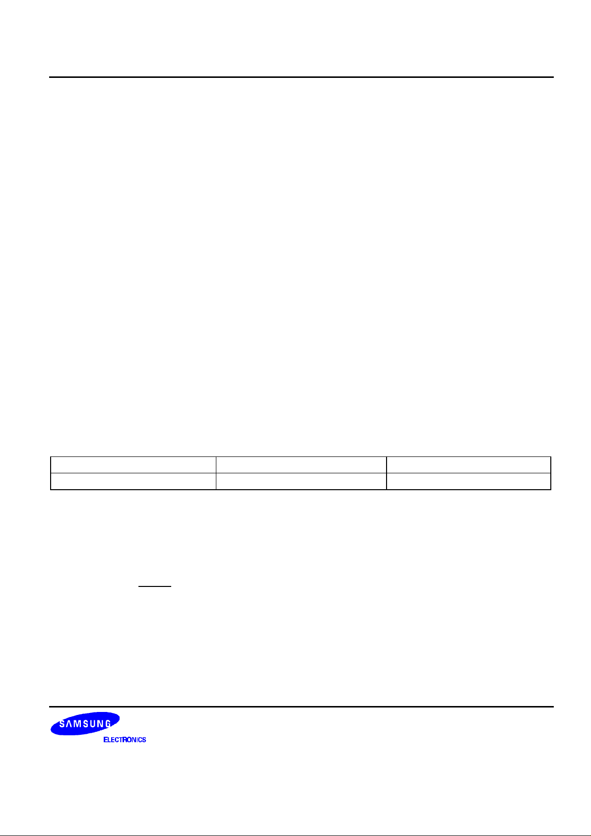
BLCOK DIAGRAM
Blue Channel
B_OUTA<7:0>
B_IN
G_IN
G_IN
Green Channel
Red Channel
CLAMP
ADC
8-bit
Output
Drver
8-bit
B_OUTB<7:0>
G_OUTA<7:0>
G_OUTB<7:0>
G_OUTA<7:0>
R_OUTB<7:0>
SDA
SCL
SEN
I2C_3W
HSYNC IN
SOG IN
VSYNC IN
CLAMP
Control
I2C and
3-wire
Sync
Processor
Gain
Control
Gain Control
CLAMP Control
PLL Control
ADC Output
Mode Control
CKA
(from PLL)
PLL
Divider
PFD
VCO
Output
Mode
CKA
Phase Shifter
HSYNC OUT
VSYNC OUT
CKA
CKB
2
TRIPLE 8-BIT ANALOG-TO-DIGITAL CONVERTER KB2516 (Preliminary)
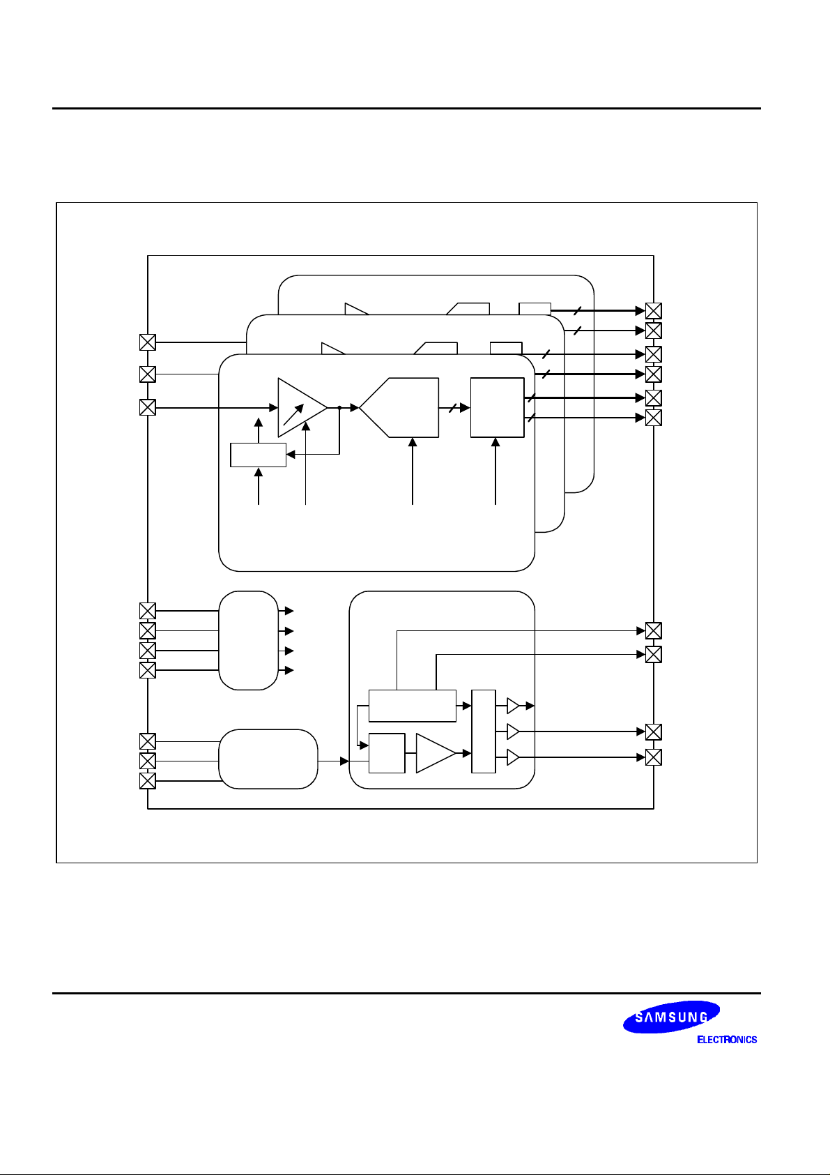
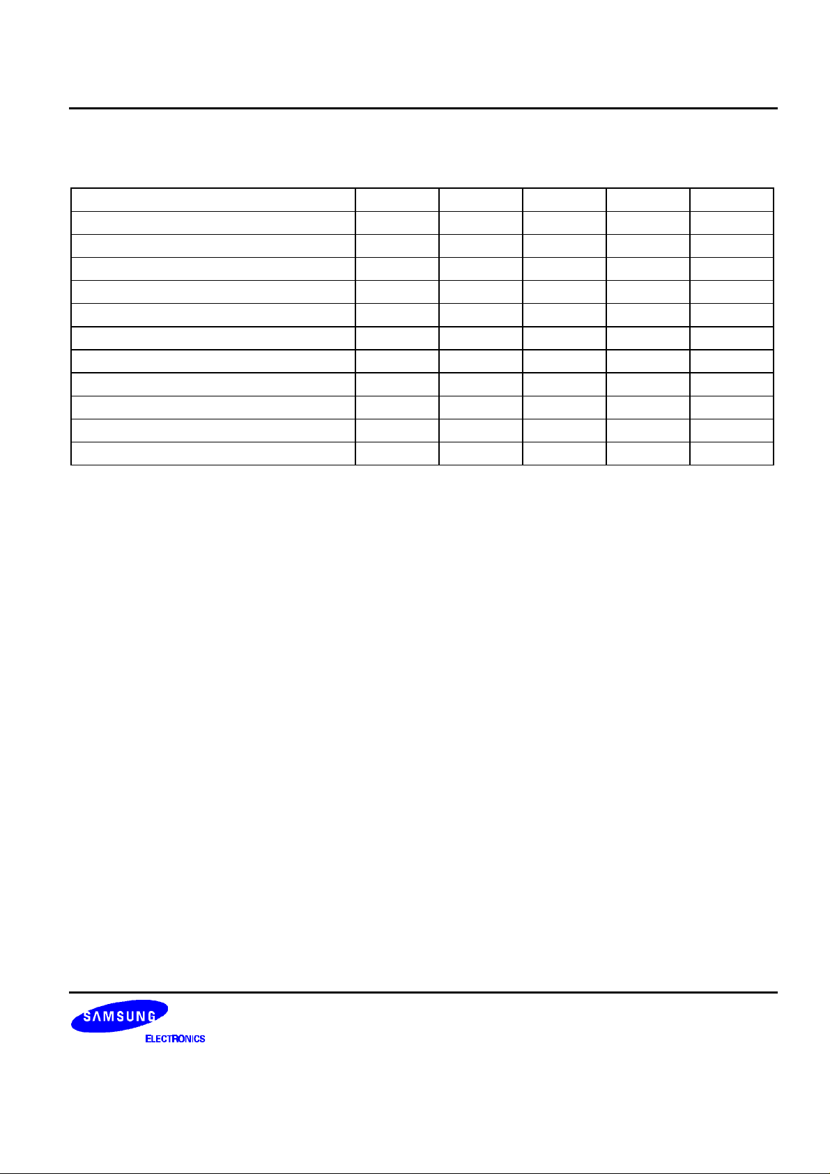
ELECTRICAL CHARACERISTICS
Symbol Parameter Conditions Min. Typ. Max. Unit
Power supply
VDDC_P Pre-amp analog supply voltage for R, G, B channels 4.75 5.0 5.25 V
VDDC_A ADC analog supply voltage for R, G, B channels 4.75 5.0 5.25 V
VDDA_A ADC analog supply voltage for R, G, B channels 3.0 3.3 3.6 V
VDDD_A ADC digital supply voltage for R, G, B channels 4.75 5.0 5.25 V
VDD_A ADC digital supply voltage for R, G, B channels 3.0 3.3 3.6 V
VDDR Output driver supply voltage for R, G, B channels 3.0 3.3 3.6 V
VDD_P PLL supply voltage 3.0 3.3 3.6 V
VDD_S Interface logic supply voltage 3.0 3.3 3.6 V
IDDC_P Pre-amp analog supply current 55 65 75 mA
IDDC_A ADC analog supply current 5V supply - 66 - mA
IDDA_A ADC analog supply current 3.3V supply - 33 - mA
IDDD_A ADC digital supply current 5V supply - 10 - mA
IDD_A ADC digital supply current 3.3V supply - 20 - mA
IDDR Output driver supply current Fclk = 140MHz, ramp input mA
IDD_P PLL supply current Fclk = 100MHz - 76 - mA
IDD_S Interface logic supply current - - mA
Ptot Total power consumption Fclk = 180MHz, ramp input - 1.25 - W
Pre-amp
f-3dB Amplifier bandwidth for R, G, B channels - 500 - MHz
VIN RGB input voltage range 0.5 0.7 1.0 Vpp
Vbs Input bias voltage for R, G, B channels 1.7 1.9 2.1 V
AVmax Voltage gain max 1.6 2.3 2.9 dB
∆AcG
∆Af1
∆Af2
tr Pre-amp rising time for R, G, B channels - 1 - nS
tf Pre-amp falling time for R, G, B channels - 1 - nS
Vbrt1
Vbrt2
Vbrt3
Coarse gain diff. between ch. for R, G, B channels -1.0 0.0 1.0 dB
Fine gain diff. 1 between ch. for R, G, B channels -1.0 0.0 1.0 dB
Fine gain diff. 2 between ch. for R, G, B channels -1.0 0.0 1.0 dB
Brightness voltage
Brightness voltage
Brightness voltage
(1)
(2)
(3)
for R, G, B channels - 1.5 - V
for R, G, B channels - 2.3 - V
for R, G, B channels - 3.0 - V
NOTES:
1. Coarse BRT = 80, Fine BRT = 00
2. Coarse BRT = 80, Fine BRT = 80
3. Coarse BRT = 80, Fine BRT = FF
3
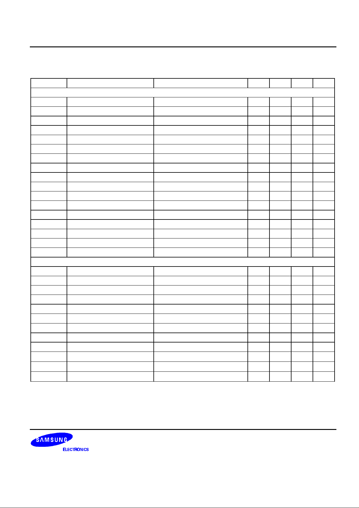
KB2516 (Preliminary) TRIPLE 8-BIT ANALOG-TO-DIGITAL CONVERTER
Symbol Parameter Conditions Min. Typ. Max. Unit
Sync processor
SOGdet1 SOG sync detect level 1 0.1 - - V
SOGdet2 SOG sync detect level 2 - - 1.0 V
Analog-to-digital converter
VrefT Reference top voltage 1.7 1.8 1.9 V
VrefB Reference bottom voltage 1.2 1.3 1.4 V
INL DC integral non-linearity Fclk = 75MHz, ramp input -1.0 - 1.0 LSB
DNL DC differential non-linearity Fclk = 75MHz, ramp input -0.5 - 0.5 LSB
SNDR Signal to noise & distortion
Fclk = 100MHz 36 - - dB
ratio
MAXrate Max. conversion rate 170 - - MHz
CT Cross talk Fclk = 100MHz - - -36 dB
trD Digital output rising time - - 2 nS
tfD Digital output falling time - - 2 nS
Phase-locked loop
fref PLL reference clock frequency 20 - 150 KHz
fclk Maximum clock frequency 180 MHz
DRpll PLL divider ratio 512 - 4095
fvco VCO output clock frequency 17 197 MHz
tcap PLL capture time In start-up condition - 4 - ms
trcap PLL re-capture time In lock condition - - 300 us
Φstep
j
PLL
Phase shift step
Tamb = 25°C
PLL jitter Fclk = 180MHz - 200 - ps
- 7.5 - deg
4
TRIPLE 8-BIT ANALOG-TO-DIGITAL CONVERTER KB2516 (Preliminary)
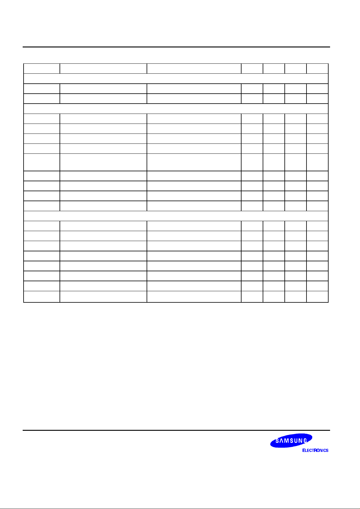
DIGITAL SPECIFICATIONS
Characteristics Symbol Min Typ Max Unit
Logic input
High level input voltage VIH VDD - 0.5 - - V
Low level input voltage VIL - - VSS + 0.5 V
High level input current IIH - 10 - uA
Low level input current IIL - 10 - UA
Input capacitance CIN - 5 - pF
Logic output
High level output voltage VOH VDD - 0.5 - - V
Low level output voltage VOL - - VSS + 0.5 V
High level input current IOH - 100 - uA
Low level input current IOL - 100 - uA
5
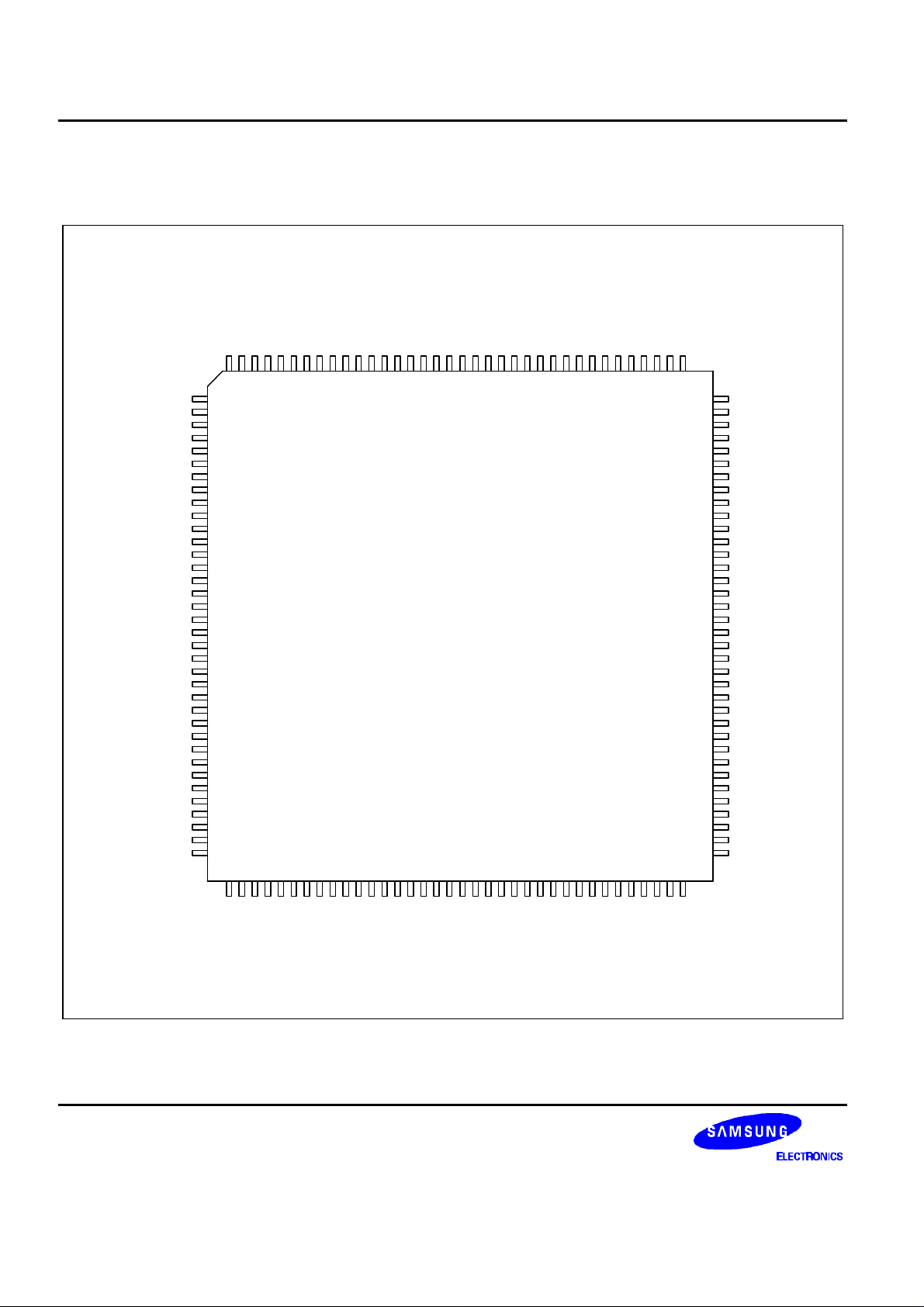
KB2516 (Preliminary) TRIPLE 8-BIT ANALOG-TO-DIGITAL CONVERTER
PIN ASSIGNMENT
VSSC_AR
VDDC_AR
ITEST
VDD_DAC
VSS_DAC
VBB2
VDDD_A
VSSD_A
VINP
VINN
VREFT
VREFB
VDDG
VSSG
PDB
RESETB_EX
HSYNCO
ADC_CKB
ADC_CK
VSYNCO
VDD_A
VSS_A
NC2
NC1
VSSR_RA
VDDR_RA
R_OUTA0
R_OUTA1
R_OUTA2
R_OUTA3
R_OUTA4
R_OUTA5
R_OUTA6
R_OUTA7
VSSR_RB
VDDR_RB
144
143
142
141
140
139
138
137
136
135
134
133
132
131
130
129
128
127
126
125
124
123
122
121
120
119
118
117
116
115
114
113
112
111
110
VDDA_AR
VSSA_AR
R_IN
VDDC_PR
R_VOUT1
VSSC_PR
R_CLPC
VDDC_AG
VSSC_AG
VDDA_AG
VSSA_AG
G_IN
VDDC_PG
G_VOUT1
VSSC_PG
G_CLPC
VDDC_AB
VSSC_AB
VDDA_AB
VSSA_AB
VSSA_AB
VDDC_PB
B_VOUT1
VSSC_PB
B_CLPC
VDDC_SP
VSSC_SP
CLPex
DETCAP
SOG_IN
HSYNC_IN
HSmic
SOGOUT
VDD_SI
VSS_SI
I2C_3W
1
2
3
4
5
6
7
8
9
10
11
12
13
14
15
16
17
18
19
20
21
22
23
24
25
26
27
28
29
30
31
32
33
34
35
36
3738394041424344454647484950515253545556575859606162636465666768697071
KB2516
144-TQFP-2020
109
108
107
106
105
104
103
102
101
100
72
99
98
97
96
95
94
93
92
91
90
89
88
87
86
85
84
83
82
81
80
79
78
77
76
75
74
73
R_OUTB0
R_OUTB1
R_OUTB2
R_OUTB3
R_OUTB4
R_OUTB5
R_OUTB6
R_OUTB7
VDDR_GA
VSSR_GA
G_OUTA0
G_OUTA1
G_OUTA2
G_OUTA3
G_OUTA4
G_OUTA5
G_OUTA6
G_OUTA7
G_OUTB0
G_OUTB1
G_OUTB2
G_OUTB3
G_OUTB4
G_OUTB5
G_OUTB6
G_OUTB7
VDDR_GB
VSSR_GB
B_OUTA0
B_OUTA1
B_OUTA2
B_OUTA3
B_OUTA4
B_OUTA5
B_OUTA6
B_OUTA7
SCL
SDA
ADDR_EX0
ADDR_EX1
SEN
COAST
VSS_PP
VDD_PP
VDD_PV
ADC_CKEX
VCTRL
ITEST1
VSS_PC
VDD_PC
VDD_PO
VSS_PO
VSS_PK
VSS_PD
VDD_PD
CKB
VDD_PK
CKC
VBB1
VSSR_BB
B_OUTB7
B_OUTB7
VDDR_BB
B_OUTB6
B_OUTB5
B_OUTB4
B_OUTB3
B_OUTB2
B_OUTB1
VSSR_BA
B_OUTB0
VDDR_BA
6

TRIPLE 8-BIT ANALOG-TO-DIGITAL CONVERTER KB2516 (Preliminary)
PIN DESCRIPTION
Table 1. Pin Description
No Name Description
1 VSSC_AR Red channel ADC 0V analog power supply
2 VDDC_AR Red channel ADC 5V analog power supply
3 R_IN Red channel analog input signal
4 VDDC_PR Red channel pre-amp 5V power supply
5 R_VOUT1 Red channel pre-amp output signal
6 VSSC_PR Red channel pre-amp 0V power supply
7 R_CLPC Red channel clamp control external cap.
8 VDDA_AG Green channel ADC 3.3V analog power supply
9 VSSA_AG Green channel ADC 0V analog power supply
10 VSSC_AG Green channel ADC 0V analog power supply
11 VDDC_AG Green channel ADC 5V analog power supply
12 G_IN Green channel analog input signal
13 VDDC_PG Green channel pre-amp 5V power supply
14 G_VOUT1 Green channel pre-amp output signal
15 VSSC_PG Green channel pre-amp 0V power supply
16 G_CLPC Green channel clamp control external cap.
17 VDDA_AB Blue channel ADC 3.3V analog power supply
18 VSSA_AB Blue channel ADC 0V analog power supply
19 VSSC_AB Blue channel ADC 0V analog power supply
20 VDDC_AB Blue channel ADC 5V analog power supply
21 B_IN Blue channel analog input signal
22 VDDC_PB Blue channel pre-amp 5V power supply
23 B_VOUT1 Blue channel pre-amp output signal
24 VSSC_PB Blue channel pre-amp 0V power supply
25 B_CLPC Blue channel clamp control external cap.
26 VDDC_SP SyncProc 5V power supply
27 VSSC_SP SyncProc 0V power supply
28 CLPex External clamp signal input pin
29 DETCAP SOG polarity output
30 SOG_IN SOG signal input pin
31 HSYNC_IN HSYNC signal input pin
32 Test
7
KB2516 (Preliminary) TRIPLE 8-BIT ANALOG-TO-DIGITAL CONVERTER
Table 1. Pin Description (Continued)
No Name Description
33 SOGOUT SOG output signal pin
34 VDD_SI Serial interface 3.3V digital power supply
35 VSS_SI Serial interface 0V digital power supply
36 I2C_3W
Serial interface mode selection between I2C and 3-wire
37 ADDR_EX0 Slave address control bit
38 ADDR_EX1 Slave address control bit
39 SDA Serial interface data signal pin
40 SCL Serial interface clock signal pin
41 SEN Signal enable for 3-wire serial interface
42 COAST COAST signal input
43 ADC_CKEX External analog to digital converter clock input
44 VDD_PP PLL 3.3V phase detector power supply
45 VSS_PP PLL 0V phase detector power supply
46 VSS_PV PLL 0V analog power supply
47 VDD_PV PLL 3.3V analog power supply
48 VCTRL VCO control voltage
49 ITEST1 Bandgap reference current test pin
50 VDD_PC PLL 3.3V charge-pump power supply
51 VSS_PC PLL 0V charge-pump power supply
52 VDD_PO PLL 3.3V VCO power supply
53 VSS_PO PLL 0V VCO power supply
54 VDD_PD PLL 3.3V digital power supply
55 VSS_PD PLL 0V digital power supply
56 VSS_PK PLL 0V clock driver power supply
57 CKB PLL output clock with ADC frequency (phase control available)
58 VDD_PK PLL 3.3V clock driver power supply
59 CKC PLL output clock with ADC frequency (phase control available)
60 VBB1 Substrate 0V power supply
61 VSSR_BB Blue channel ADC output B driver power supply (0V)
62 VDDR_BB Blue channel ADC output B driver power supply (3.3V)
63 B_OUTB7 Blue channel ADC digital output B bit 7
64 B_OUTB6 Blue channel ADC digital output B bit 6
65 B_OUTB5 Blue channel ADC digital output B bit 5
66 B_OUTB4 Blue channel ADC digital output B bit 4
67 B_OUTB3 Blue channel ADC digital output B bit 3
8
TRIPLE 8-BIT ANALOG-TO-DIGITAL CONVERTER KB2516 (Preliminary)
Table 1. Pin Description (Continued)
No Name Description
68 B_OUTB2 Blue channel ADC digital output B bit 2
69 B_OUTB1 Blue channel ADC digital output B bit 1
70 B_OUTB0 Blue channel ADC digital output B bit 0
71 VSSR_BA Blue channel ADC output A driver power supply (0V)
72 VDDR_BA Blue channel ADC output A driver power supply (3.3V)
73 B_OUTA7 Blue channel ADC digital output A bit 7
74 B_OUTA6 Blue channel ADC digital output A bit 6
75 B_OUTA5 Blue channel ADC digital output A bit 5
76 B_OUTA4 Blue channel ADC digital output A bit 4
77 B_OUTA3 Blue channel ADC digital output A bit 3
78 B_OUTA2 Blue channel ADC digital output A bit 2
79 B_OUTA1 Blue channel ADC digital output A bit 1
80 B_OUTA0 Blue channel ADC digital output A bit 0
81 VSSR_GB Green channel ADC output B driver power supply (0V)
82 VDDR_GB Green channel ADC output B driver power supply (3.3V)
83 G_OUTB7 Green channel ADC digital output B bit 7
84 G_OUTB6 Green channel ADC digital output B bit 6
85 G_OUTB5 Green channel ADC digital output B bit 5
86 G_OUTB4 Green channel ADC digital output B bit 4
87 G_OUTB3 Green channel ADC digital output B bit 3
88 G_OUTB2 Green channel ADC digital output B bit 2
89 G_OUTB1 Green channel ADC digital output B bit 1
90 G_OUTB0 Green channel ADC digital output B bit 0
91 G_OUTA7 Green channel ADC digital output A bit 7
92 G_OUTA6 Green channel ADC digital output A bit 6
93 G_OUTA5 Green channel ADC digital output A bit 5
94 G_OUTA4 Green channel ADC digital output A bit 4
95 G_OUTA3 Green channel ADC digital output A bit 3
96 G_OUTA2 Green channel ADC digital output A bit 2
97 G_OUTA1 Green channel ADC digital output A bit 1
98 G_OUTA0 Green channel ADC digital output A bit 0
99 VSSR_GA Green channel ADC output A driver power supply (0V)
100 VDDR_GA Green channel ADC output A driver power supply (3.3V)
101 R_OUTB7 Red channel ADC digital output B bit 7
102 R_OUTB6 Red channel ADC digital output B bit 6
9
 Loading...