

Samsung KA2511B Datasheet

MARCH. 1998
DATA SHEET
KB2511B
DEFLECTION PROCESSOR FOR MULTISYNC MONITORS KB2511B
1
DEFLECTION PROCESSOR
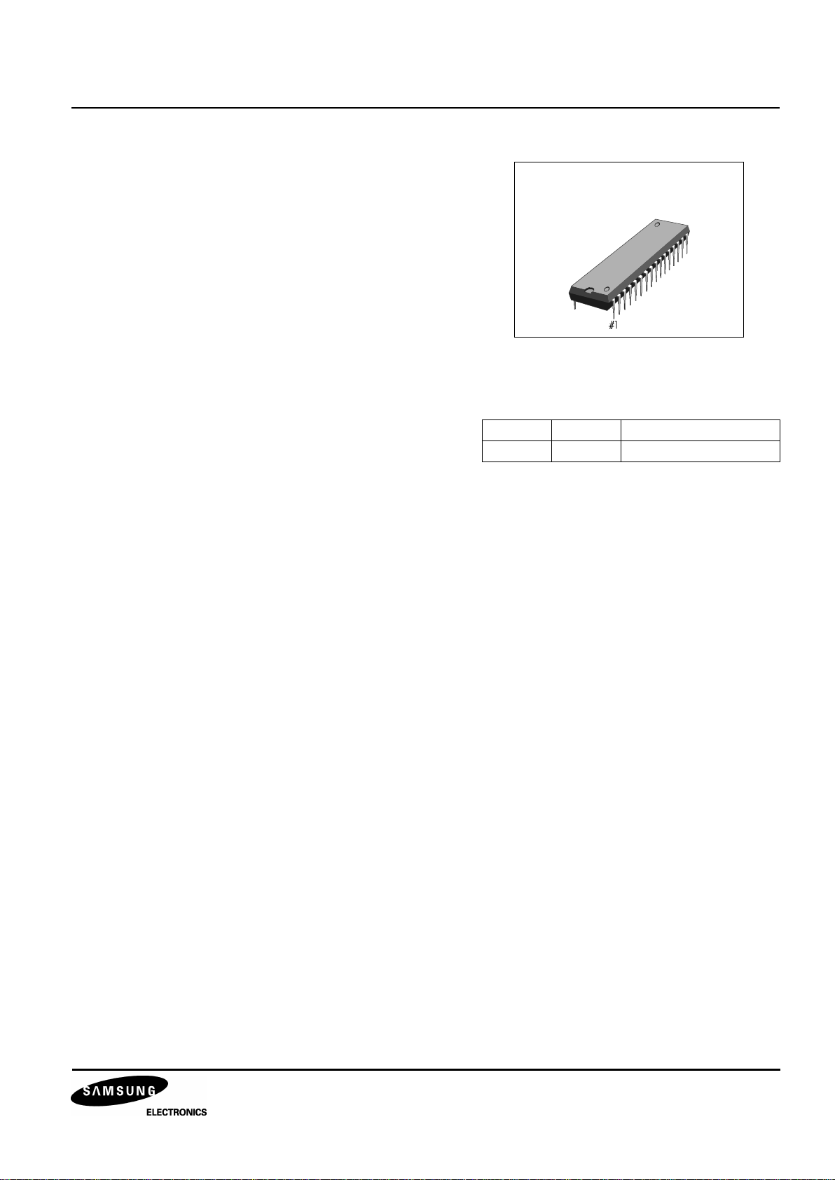
The KB2511B is a monolithc integrated circuit assembled in 32 pins shrunk dual in line plastic package. This
IC controls all the functions related to the horizontal and
vertical deflection in multimodes or multi-frequency computer display monitors.
The internal sync processor, combined with the very
powerful geometry correction block make the KB2511
suitable for very high performance monitors with very
few external components. The horizontal jitter level is
very low. It is particularly well suited for high-end 15”
and 17” monitors.
FUNCTIONS
• Defiection Processor
• I2C BUS Control
• B+ Regulator
• Vertical Parabola Generator
• Horizontal and Vertical dynamic focus
FEATURES
(HORIZONTAL)
• Self-adaptative
• Dual PLL concept
• 150kHz maximum frequency
• X-RAY protection input
• I2C controls : Horizontal duty-cycle, H-position,free running
frequency, frequency generator for burn-in mode.
(VERTICAL)
• Vertical ramp generator
• 50 to 165Hz AGC loop
• Geometry tracking with V-POS & AMP
• I2C Controls :
V-AMP, V-POS, S-CORR, C-CORR
(I2C GEOMETRY CORRECTIONS)
• Vertical parabola generator
(Pincushion-E/W, Keystone)
• Horizontal Dynamic Phase
(Side Pin balance & parallelogram)
• Horizontal and vertical dynamic focus
(Horizontal Focus Amplitude, Horizontal
Focus Symmetry, Vertical Focus Amplitude)
(GENERAL)
• Sync Processor
• 12V supply voltage
• Hor. & Vert, lock/unlock outputs
• Read/Write I2C interface
• Vertical moire
• B+ Regulator
-Internal PWM generator for B+ current mode
step-up converter.
- Switchable to step-down converter
- I2C adjustable B+ reference voltage
- Output pulses synchronized on horizontal
frequency
ORDERING INFORMATION
Device Package Operating Temperature
KB2511B 32-SDIP 0 °C ~ 70 °C
32-SDIP-400
KB2511B DEFLECTION PROCESSOR FOR MULTISYNC MONITORS
2
BLOCK DIAGRAM
19
16
15
28
14
9
PHASE/
FREQUENCY
COMPARATOR
H-PHASE(7 bits)
LOCK/UNLOCK
IDENTIFICATION
PHASE
COMPARATOR
VCO
SAFETY
PROCESSOR
PHASE
SHIFTER
H-DUTY
(5 bits)
7
3
8
5
6 12 4
B+
CONTROLLER
10
I C INTERFACE
GEOMETRY
TRACKING
22 20
23
VACCAP
COMP
PLL1F
HLOCKOUT
R0
C0
HFLY
PLL2C
HOUT
VOUT
VREF
Forced
Freq.
2 bits
Free running
5 bits
HOUT
BUFFER
26
13
SYNC INPUT
SELECT
(1bit)
SYNC
PROCESSOR
V
REF
21
1
2
25
29
27
30
31
32
Vcc
XRAY
RESET
GENERATOR
2
X
2
X
2
MOIRE
CANCEL
5 BITS+ON/OFF
+
+
+
17
+
24
B+ ADJUST
7 bits
VSYNC
S AND C
CORRECTION
VERTICAL
OSCILLATOR
RAMP GENERATOR
6 bits 8 bits
VPOS
7bits
keyst
6 bits
PCC
7 bits
VAMP
6 bits
X
2
X
X
2
Amp & symmetry
2x5 bits
Spin Bal
6 bits
Key Bal
6 bits
VAMP
7 bits
H POSITION
B+ OUT
REGIN
BGND
HFOCUS
CAP
FOCUS
ISENSE
EWOUT
VCAP
H/HVIN
HREF
VSYNC
IN
VCC
XRAY
VREF
VGND
5V
SDA
SCL
GND
11
HGND
18
BREATH
DEFLECTION PROCESSOR FOR MULTISYNC MONITORS KB2511B
3
PIN CONFIGURATIONS
VREF
SDA
SCL
C0
R0
HPOSITION
PLL1F
PLL2C
XRAY
HOUT
VGND
EWOUT
VCC
GND
9
3
2
1
6
5
8
7
27
21
31
30
25
26
10
19
29
24
VAGCCAP
COMP
HFLY
4
14
12
28
HFOCUSCAP
HLOCKOUT
VSYNCIN
H/HVIN
13
FOCUSOUT
HREF
11
HGND
20
BOUT
5V
VOUT
32
22
VCAP
23
KB2511B
15
16
18
17
REGIN
ISENSE
BREATH
B+GND
KB2511B DEFLECTION PROCESSOR FOR MULTISYNC MONITORS
4
PIN DESCRIPTION
Table 1. Pin Description
No Pin Name Description
1 H/HVIN TTL compatible horizontal sync input(Separate or composite)
2 VSYNCIN TTL compatible vertical sync input (for separated H&V)
3 HLOCKOUT First PLL lock/unlock output (0V unlocked - 5V locked)
4 PLL2C Second PLL loop filter
5 C0 Horizontal oscillator capacitor
6 R0 Horizontal oscillator resistor
7 PLL1F First PLL loop filter
8 HPOSITION Horizontal position filter(Capacitor to be connected to HGND)
9 HFOCUSCAP Horizontal dynamic focus oscillator capacitor
10 FOCUSOUT Mixed horizontal and vertical dynamic focus output
11 HGND Horizontal Section Ground
12 HFLY Horizontal Flyback Input (positive polarity)
13 HREF Horizontal Section Reference Voltage (to be filtered)
14 COMP B+ error amplifier output for frequency compensation and gain setting
15 REGIN Regulation input of B+ control loop
16 ISENSE Sensing of external B+ switching transistor current or switch for step-down converter
17 B+GND Ground (related to B+ reference adjustment)
18 BREATH DC breathing input control(Compensation of vertical amplitude against EHV variation)
19 VGND Vertical section ground
20 VAGCCAP Memory capacitor for automatic gain control loop in vertical ramp generator
21 VREF Vertical section reference voltage (to be filtered)
22 VCAP Vertical sawtooth generator capacitor
23 VOUT Vertical ramp output (with frequency independant amplitude and S or C corrections if any).
It is mixed with vertical position voltage and vertical moire.
24 EWOUT Pincushion-East/West correction parabola output
25 XRAY X-RAY protection input (with internal latch function)
26 HOUT Horizontal drive output (internal transistor, open collector)
27 GND General ground (referenced to Vcc)
28 BOUT B+ PWM regulator output
29 Vcc Supply voltage (12V typ)
30 SCL
I2C clock input
31 SDA
I2C data input
32 5V Supply voltage (5V typ)
DEFLECTION PROCESSOR FOR MULTISYNC MONITORS KB2511B
5
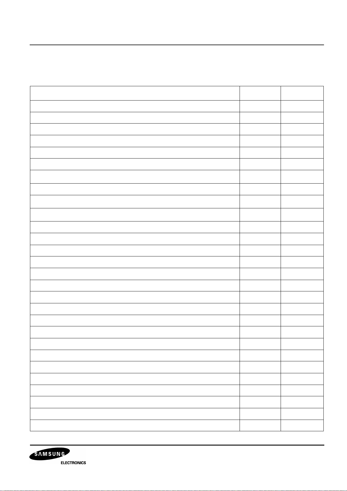
REFERENCE DATA
Table 2. Reference Data
Parameter Value Unit
Horizontal frequency 15 to 150 kHz
Autosynch frequency (for given R0 and C0) 1 to 4.5FO FH
± Horizontal sync polarity input YES
Polarity detection (on both horizontal and vertical section) YES
TTL Composite synch YES
Lock/Unlock identification (on both horizontal 1st PLL and vertical section) YES
I2C control for H-Position
±10 %
XRay protection YES
I2C horizontal duty cycle adjust
30 to 60 %
I2C free running frequency adjustment
0.8 to 1.3FO FH
Stand-by function YES
Dual polarity H-Drive outputs NO
Supply voltage monitoring YES
PLL1 inhibition possibility NO
Blanking output NO
Vertical frequency 35 to 200 Hz
Vertical autosync (for 150nF on Pin22 and 470nF on Pin20) 50 to 165 Hz
Vertical S-Correction YES
Vertical C-Correction YES
Vertical amplitude adjustment YES
DC breathing control on Vertical amplitude YES
East/West parabola output(also known as Pin cushion output) YES
East/West correction amplitude adjustment YES
Keystone adjustment YES
Internal dynamic horizontal phase control YES
Side pin balance amplitude adjustment YES
Parallelogram adjustment YES
Tracking of geometric corrections with vertical amplitude and position YES
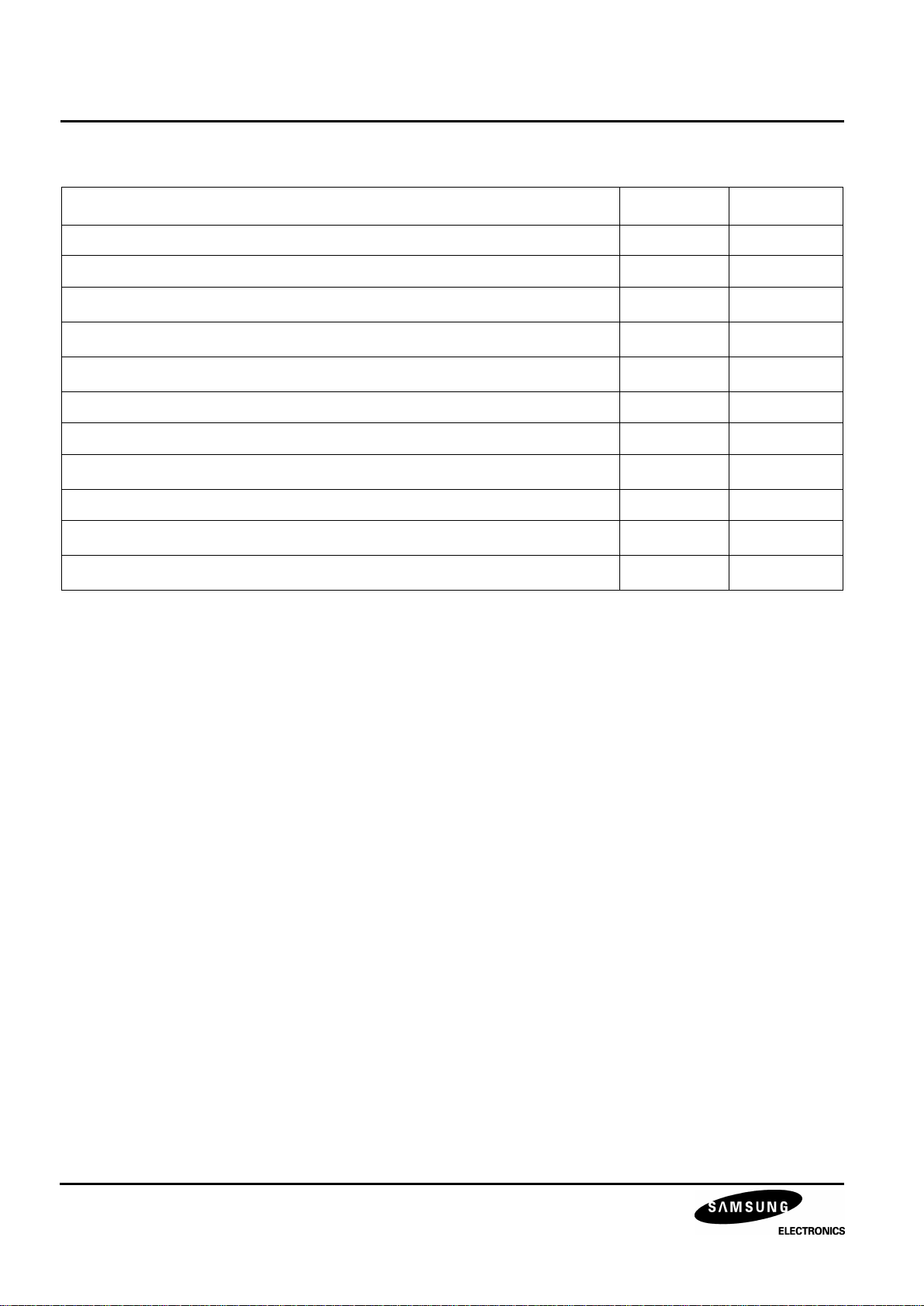
KB2511B DEFLECTION PROCESSOR FOR MULTISYNC MONITORS
6
Reference voltage (both on horizontal and vertical) YES
Dynamic focus (both on horizontal and vertical) YES
I2C horizontal dynamic focus amplitude adjustment
YES
I2C horizontal dynamic focus symmetry adjustment
YES
I2C vertical dynamic focus amplitude adjustment
YES
Deflection of input Sync type(biased from 5V alone) YES
Vertical moire output YES
I2C controlled V-moire amplitude
YES
Frequency generator for burn-in YES
Fast I2C read/write
400 kHz
B+ regulation adjustable by I2C
YES
Table 2. Reference Data (Continued)
Parameter Value Unit
DEFLECTION PROCESSOR FOR MULTISYNC MONITORS KB2511B
7
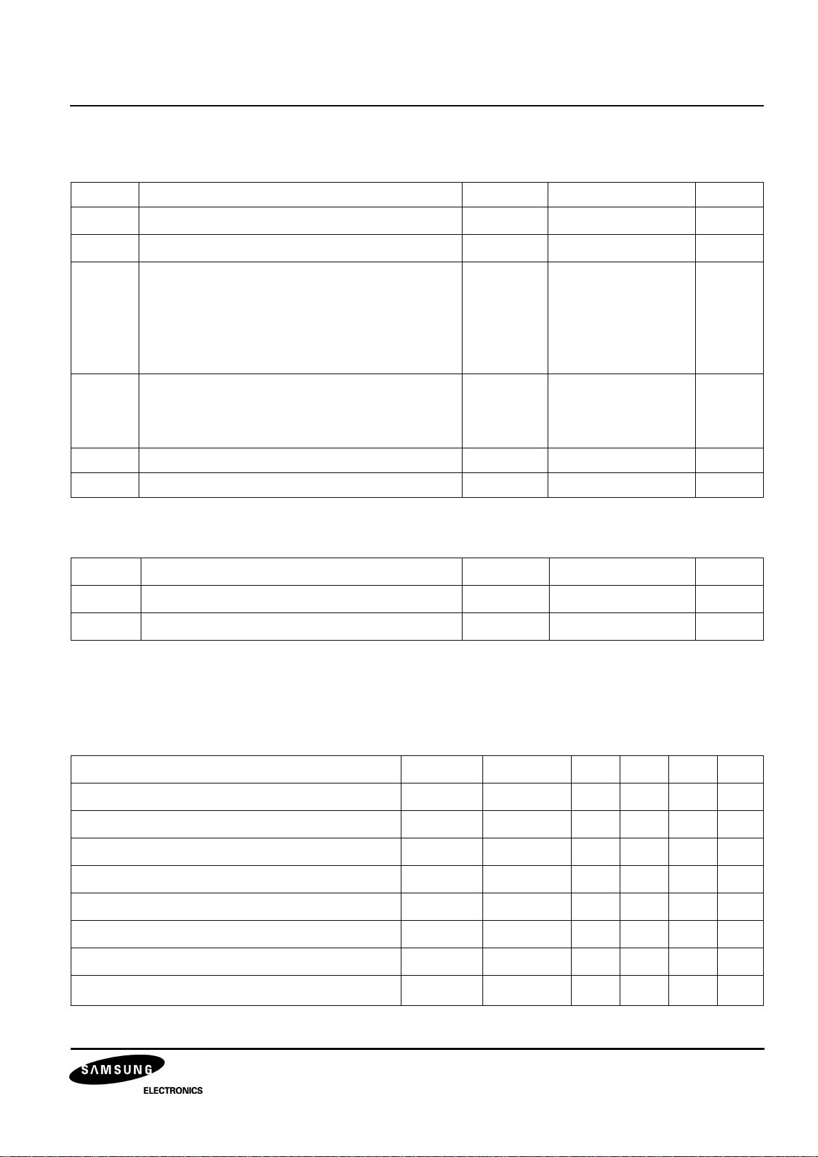
ABSOLUTE MAXIMUM RATINGS
THERMAL CHARACTERISTICS
SYNC PROCESSOR
OPERATING CODNITIONS
No Item Symbol Value Unit
1 Supply voltage (pin 29) V
CC
13.5 V
2 Supply voltage (pin 32) V
DD
5.7 V
3 Maximum voltage on Pin 4
Pin 9
Pin 5
Pins 6,7,8,14,15,16,20,22
Pins 10,18,23,24,25,26,28
Pins 1,2,3,30,31
V
IN
4.0
5.5
6.4
8.0
V
CC
V
DD
V
V
V
4 ESD susceptibillty
Human body model, 100pF discharge through
1.5KΩ
EIAJ norm, 200pF discharge through 0Ω
VESD 2
300
kV
V
5 Storage temperature Tstg - 40, +150 °C
6 Operating temperature Topr 0, +70 °C
No Item Symbol Value Unit
1 Junction temperature Tj +150 °C
2 Junction-ambient thermal resistance θja 65 °C/W
Table 3. Sync Processor Operating Codnitions
Parameter Symbol Conditions Min Typ Max Unit
Horizontal sync input voltage HsVR Pin 1 0 5 V
Minimum horizontal input pulse duration MinD Pin 1 0.7 µs
Maximum horizontal input signal duty cycle Mduty Pin 1 25 %
Vertical sync input voltage VsVR Pin 2 0 5 V
Minimum vertical sync pulse width VSW Pin 2 5 µs
Maximum vertical sync input duty cycle VSmD Pin 2 15 %
Maximum vertical sync width on TTL H/V composite VextM Pin 1 750 µs
Sink and source current
I
HLOCKOUT
Pin 3 250 µA
KB2511B DEFLECTION PROCESSOR FOR MULTISYNC MONITORS
8
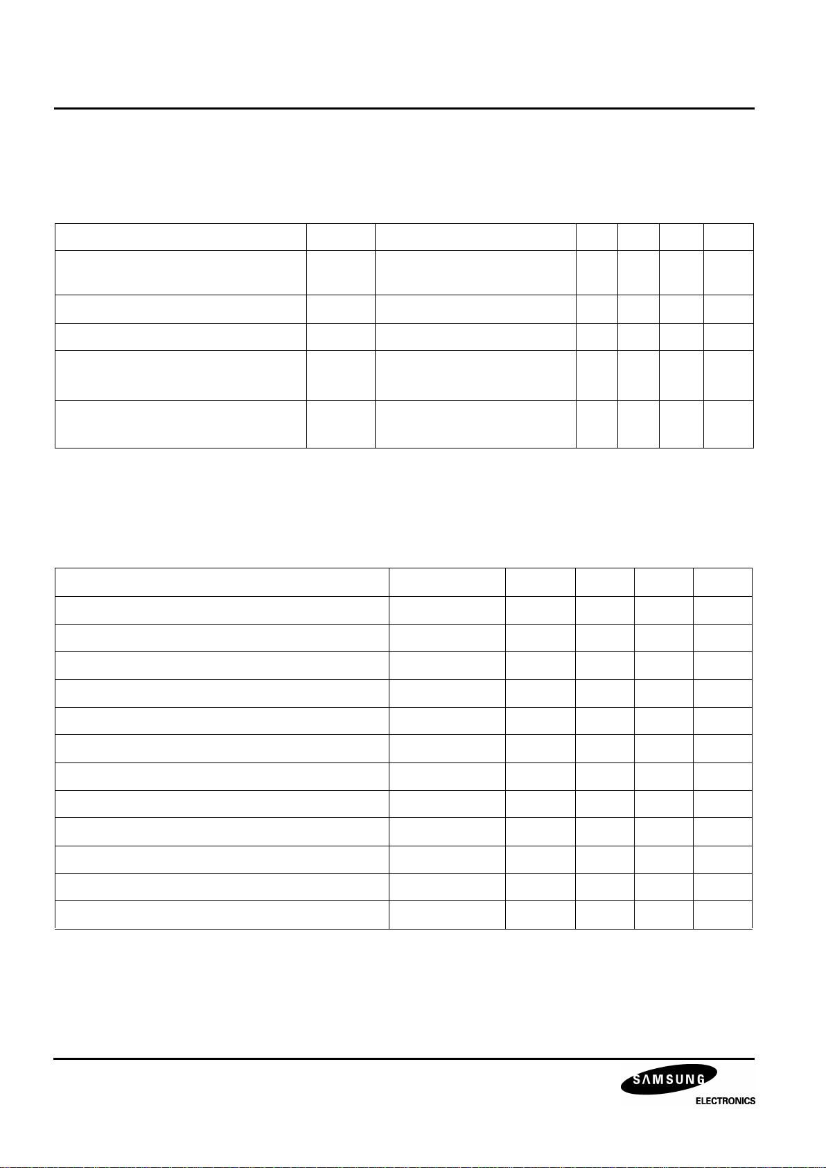
ELECTRICAL CHARACTERISTICS
( VDD = 5V, Tamb = 25 °C )
I2C READ/WRITE(See also I
2
C table control and I2C sub address control)
OPERATING CONDITIONS
Table 4. Sync Processor Electrical Characteristics
Parameter Symbol Conditions Min Typ Max Unit
Horizontal and vertical input threshold
voltage (pin 1, 2)
VINTH
Low level
High level 2.2
0.8 V
V
Horizontal and vertical pull-up resister RIN pins 1,2 200 KΩ
Falling and rising output CMOS buffer TfrOut pin 3, Cout = 20pF 200 ns
Horizontal 1st PLL lock output status
(pin 3)
VHlock
Locked, I
LOCKOUT
= -250µA
Unlocked, I
LOCKOUT
= +250µA
0
5
0.5 V
V
Extracted vsync integration time (% of
TH
(9)
) on H/V composite
VoutT C0 = 820pF 26 35 %
Table 5. I2C Read/Write Operating Conditions
Parameter Symbol Min Typ Max Unit
Input High Level Voltage VinH 3.0 - 5.0 V
Input Low Level Voltage VinL 0 - 1.5 V
SCL Clock frequency fSCL - - 200 kHz
Hold time before a new transmission can start tBUF 1.3 - - uS
Hold time for Start conditions tHDS 0.6 - - uS
Set-Up time for Stop conditions tSUP 0.6 - - uS
The Low Period of SCL tLOW 1.3 - - uS
The High Period of SCL tHIGH 0.6 - - uS
Hold time data tHDAT 0.3 - - uS
Set-Up time data tSUPDAT 0.25 - - uS
Rise time of SCL tR - - 1.0 uS
Fall time of SCL tF - - 3.0 uS
DEFLECTION PROCESSOR FOR MULTISYNC MONITORS KB2511B
9
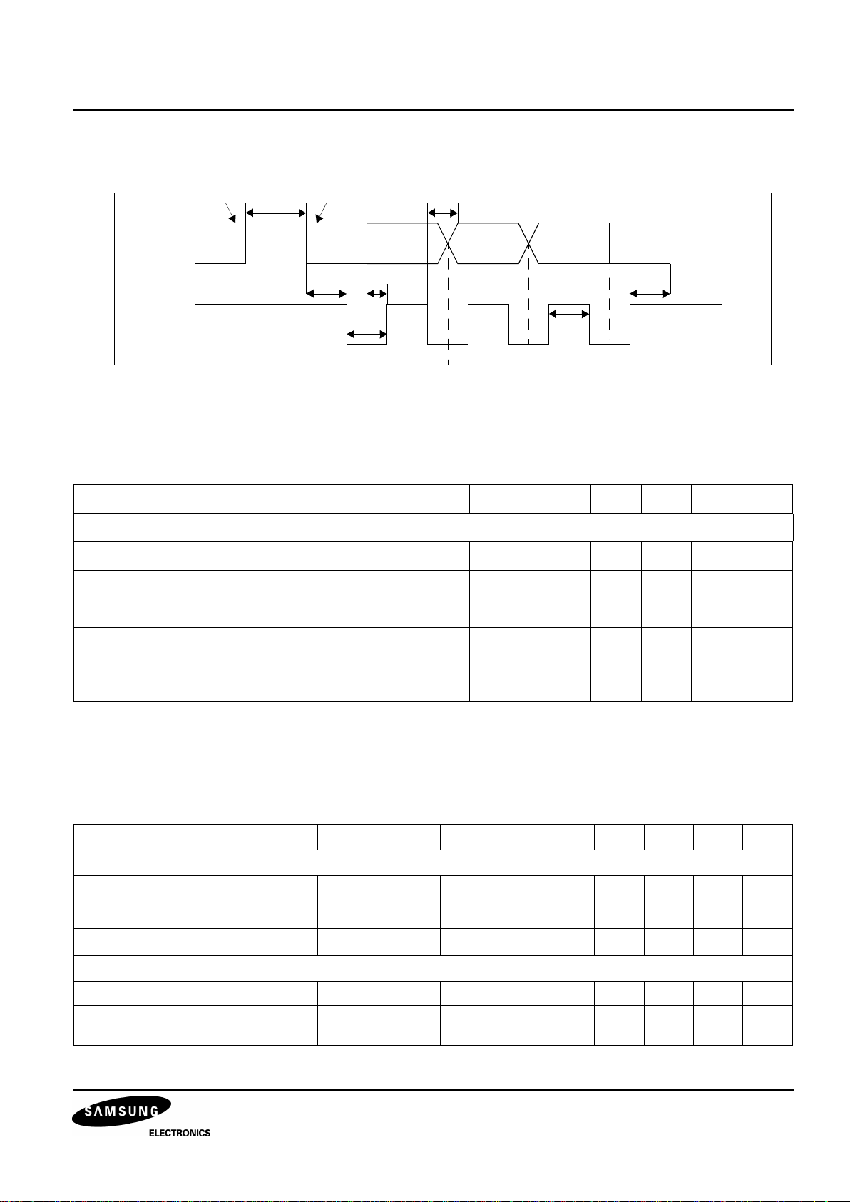
I2C BUS Timing Requirement
ELECTRICAL CHARACTERISTICS
( VDD = 5V, Tamb = 25 °C)
HORIZONTAL SECTION
OPERATING CONDITIONS
Table 6. I2C Read/Write Electrical Characteristics
Parameter Symbol Conditions Min Typ Max Unit
I2C PROCESSOR
Maximum clock frequency Fscl Pin 30 400 kHz
Low period of the SCL clock Tlow Pin 30 1.3 µs
High period of the SCL clock Thigh Pin 30 0.6 µs
SDA and SCL input threshold Vinth Pin 30, 31 2.2 V
Acknowledge output voltage on SDA input with
3mA
VACK Pin 31 0.4 V
Table 7. Horizontal Section Operating Conditions
Parameter Symbol Conditions Min Typ Max Unit
VCO
Minimum oscillator resistor R
0(Min.)
Pin 6 6 KΩ
Minimum oscillator capacitor C
0(Min.)
Pin 5 390 pF
Maximum oscillator frequency F
(Max.)
150 kHz
OUTPUT SECTION
Maximum input peak current I12m Pin 12 5 mA
Horizontal drive output maximum
current
HOI Pin26, sunk current 30 mA
tBUF
Start:Clock High
Stop:Clock High
SDA
SCL
tLOW
tHDS
tSUPDAT
Data Change:Clock Low
tSUP
tHDAT
tHIGH
KB2511B DEFLECTION PROCESSOR FOR MULTISYNC MONITORS
10
ELECTRICAL CHARACTERISTICS
( VDD = 5V, Tamb = 25 °C)
Table 8. Horizontal Section Electrical Characteristics
Parameter Symbol Conditions Min Typ Max Unit
SUPPLY AND REFERENCE VOLTAGE
Supply voltage Vcc Pin 29 10.8 12 13.2 V
Supply voltage V
DD
Pin 32 4.5 5 5.5 V
Supply current I
CC
Pin 29 50 mA
Supply current I
DD
Pin 32 5 mA
Horizontal reference voltage V
REF-H
Pin 13, I=-2mA 7.4 8 8.6 V
Vertical reference voltage V
REF-V
Pin 21, I=-2mA 7.4 8 8.6 V
Max. sourced current on V
REF-H
I
REF-H
Pin 13 5 mA
Max. sourced current on V
REF-V
I
REF-V
Pin 21 5 mA
1st PLL SECTION
Polarity integration delay HpoIT Pin 1 0.75 ms
VCO control voltage (pin 7) V
VCO
V
REF-H
=8V
f0
fH (Max.)
1.3
6.2
V
V
VCO gain (pin 7 ) V
COG
R0=6.49KΩ, C0=820pF,
dF/dV=1/11R0C
0
17 kHz/V
Horizontal phase adjustment
(11)
Hph % of horizontal period ± 10 %
Horizontal phase setting value(Pin 8)
(11)
Minimum current value
Typical value
Maximum value
Hphmin
Hphtyp
Hphmax
Sub-address 01
Byte x 1111111
Byte x 1000000
Byte x 0000000
2.6
3.2
3.8
V
V
V
PLL1 filter current charge IPII1U
IPII1L
PLL1 is unlocked
PLL1 is locked
±140
±1
µA
mA
Free running frequency fo R0=6.49KΩ,C0=820pF,
f0=0.97/8R0C
0
±140
±1
µA
mA
Free running frequency thermal drift
(no drift on external components)
(7)
dF0/dT -150 ppm/c
Free running frequency adjustment
Minimum value
Maximum value
f0(Min.)
f0(Max.)
Sub-address 02
Byte x x x 11111
Byte x x x 00000
0.8
1.3
F0
F0
PLL1 capture range CR R0=6.49KΩ,C0=820pF,
from f0+0.5KHz to 4.5Fo
fH(Min.)
fH(Max.)
100
23.5 KHz
KHz
Safe forced frequency
SF1 Byte 11 x x x x x x
SF2 Byte 10 x x x x x x
SFF Sub-address 02
2F0
3F0
2ND PLL SECTION HORIZONTAL OUTPUT SECTION
 Loading...