

Samsung KA2500 Datasheet

APRIL. 1998
DATA SHEET
KA2500
I2C BUS CONTROLLED R/G/B VIDEO AMPLIFIER FOR MONITORS KA2500
•
Clamp Gate With Anti OSD Sagging
I2C BUS CONTROLLED R/G/B VIDEO AMPLIFIER
The KA2500 is a very high frequency video amplifier
system with I2C Bus control used in Monitors with high
resolution up to1280 × 1024.
It contains 3 matched R/G/B video Amplifiers with OSD
interface and provides flexible interfacing to I2C Bus
controlled adjustment systems.
FUNCTIONS
• R/G/B Video Amplifier
• OSD Interface
• I2C BUS Control
• Contrast/OSD Contrast
• Brightness Control
• Cut-Off Brightness Control
• R/G/B SUB Contrast/Cut-Off Control
• Blank/Clamp Gate
• Half tone
• Brightness Uniformity
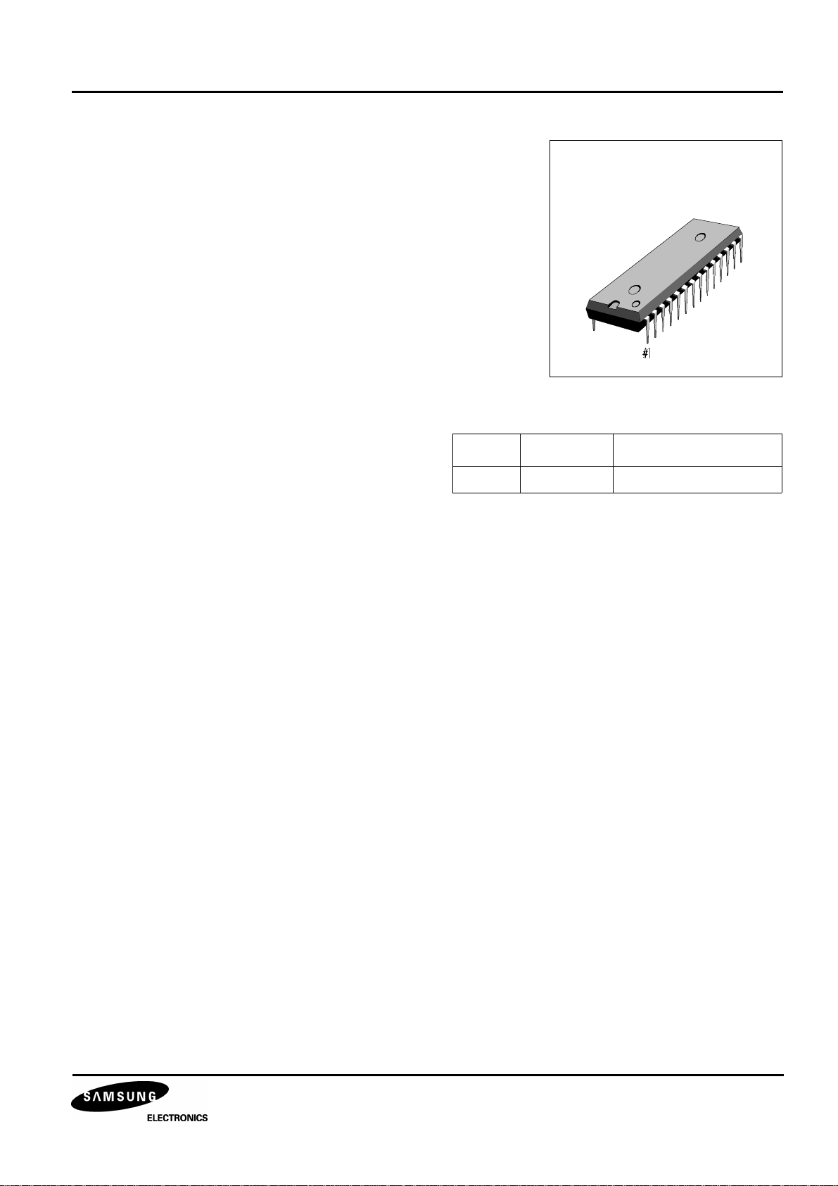
28-DIP-600A
ORDERING INFORMATION
Device Package Operating Temperature
KA2500 28-DIP-600A -20 °C ~ +75 °C
FEATURES
• 3 - Channel R/G/B Video Amplifier, 150MHz @f-3dB
• I2C Bus Control Items
- Contrast Control
- SUB Contrast Control For Each Channel
- Brightness Control
- OSD Contrast Control
- Cut-off Brightness Control
- Cut-off Control For Each Channel
- Switch Registers for SBLK and Video Half Tone and
Cut-Off INT/EXT
• SUB Contrast Control Range: -11dB
• Capable of 7.0Vpp Output Swing Range
• Video/OSD High Speed Switch
• B/U (Brightness Uniformity) Interface
• Video Input Clamp, BRT Clamp
• Video & OSD Half Tone Function on OSD
Picture
(OSD Raster Selection by HS1, 2: 4 colors)
• OSD Interface, OSD BLK
• ABL
• TTL R/G/B OSD Inputs, 80MHz bandwidth
• Contrast Control Range: -38dB
• OSD Contrast Control Range: -38dB
1
KA2500 I2C BUS CONTROLLED R/G/B VIDEO AMPLIFIER FOR MONITORS
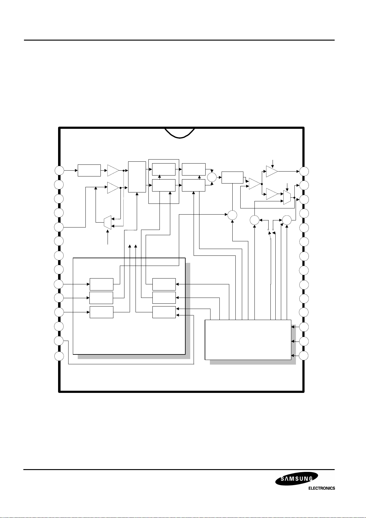
CUT OFF EXT OFFSET D3:5 (0AH)
BLOCK DIAGRAM
ROSD
GOSD
BOSD
VCC2
RIN
VCC1
GND1
GIN
B/U
VI/OSD_SW
CLP
BIN
ONE (RED)
OF THREE CHANNELS
1
2
3
9
5
6
7
8
28
4
18
10
OSD
INTERFACE
gm1
CLP
B/U
INTERFACE
VIDEO/OSD
SWITCH
CLAMP
GATE
VIDEO
OSD
SWITCH
CLP BLK
OSD
RASTER
VIDEO
HALF-TONE
HALF-TONE
VIDEO
HALF-TONE
OSD RASTER
SELECT
BLANK
GATE
OSD
CONTRAST
VIDEO
CONTRAST
VIDEO-HALF TONE SWITCH
D1(0AH)
OSD RASTER COLOR
D6:7(0AH)
SOFT BLANK
D0(0AH)
BLK
ROUT
SUB
+
CONTRAST
+
R/G/B DRIVE CONTROL (02/03/04H)
CONTRAST CONTRAL (00H)
OSD CONT CONTROL (05H)
A2
A1
A3
Cut Off
+ +
R/G/B CUT OFF CONTROL (07/08/09H)
BRIGHTNESS CONTROL (01H)
CUT OFF INT/EXT SWITCH(0AH)
26
CLP
27
gm2
17
23
22
21
20
15
CUT OFF BRIGHT (06H)
24
25
16
12
RCLP
RCT
VCC3
GND3
BOUT
BCLP
BCT
GOUT
GCLP
GCT
ABL
19
BLK
INTERFACE & CONTROL
GND(L)
2
I2C BUS CONTROL
14
SDA
13
SCL11
I2C BUS CONTROLLED R/G/B VIDEO AMPLIFIER FOR MONITORS KA2500
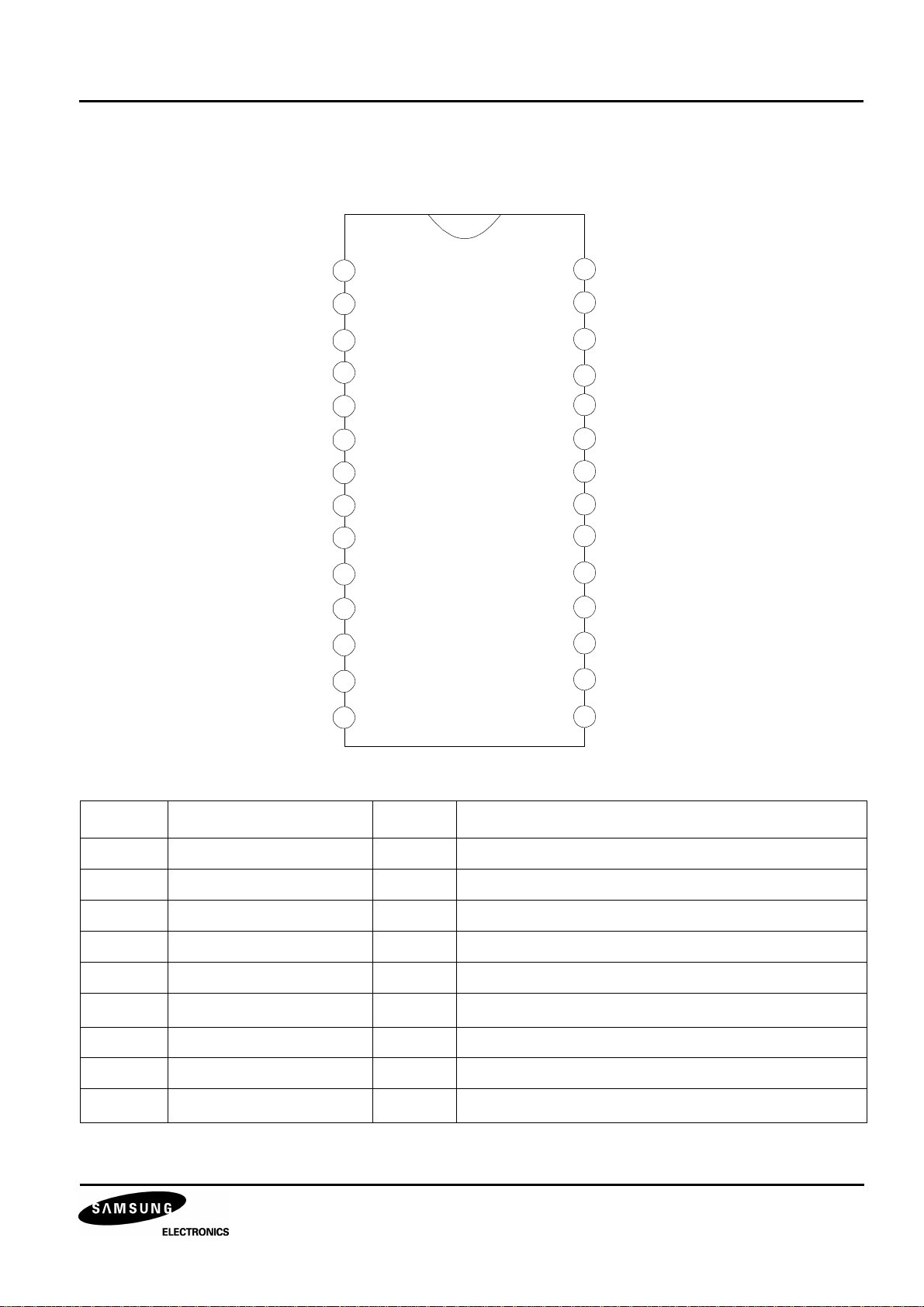
PIN CONFIGURATION
1
2
3
4
5
6
7
8
9
10
11
12
13
14
ROSD
GOSD
BOSD
VI/OSD_SW
RIN
VCC1
GND1
GIN
VCC2
BIN
GND(L)
ABL
SCL
SDA
28
B/U
27
RCLP
26
ROUT
25
GCLP
24
GOUT
VCC3
23
22
GND3
21
BOUT
20
KA2500
BCLP
BLK
CLP
RCT
GCT
BCT
19
18
17
16
15
Table 1. Pin Configuration
Pin No Symbol I/O Configuration
1 ROSD I Red OSD Input
2 GOSD I Green OSD Input
3 BOSD I Blue OSD Input
4 VI/OSD_SW I Video or OSD Switch
5 RIN I Red Video Input
6 V
CC1
- VCC (normal)
7 GND1 - Ground1 (normal)
8 GIN I Green Video Input
9 V
CC2
- VCC (normal)
3
KA2500 I2C BUS CONTROLLED R/G/B VIDEO AMPLIFIER FOR MONITORS
Table 1. Pin Configuration
Pin No Symbol I/O Configuration
10 BIN I Blue Video Input
11 GND (L) - Ground2 (logic)
12 ABL - Automatic Beam Limit
13 SCL I/O Serial Clock
14 SDA I/O Serial Data
15 BCT I Blue Cut Off Control
16 GCT I Green Cut Off Control
17 RCT I Red Cut Off Control
18 CLP I Clamp Gate Signal Input
19 BLK I Blank Gate Signal Input
20 BCLP - Blue Clamp Cap
21 BOUT O Blue Video Output
22 GND3 - Ground3 (drive part)
23 V
CC3
- VCC (drive part)
24 GOUT O Green Video Output
25 GCLP - Green Clamp Cap
26 ROUT O Red Video Output
27 RCLP - Red Clamp Cap
28 B/U I Brightness Uniformity
4
I2C BUS CONTROLLED R/G/B VIDEO AMPLIFIER FOR MONITORS KA2500
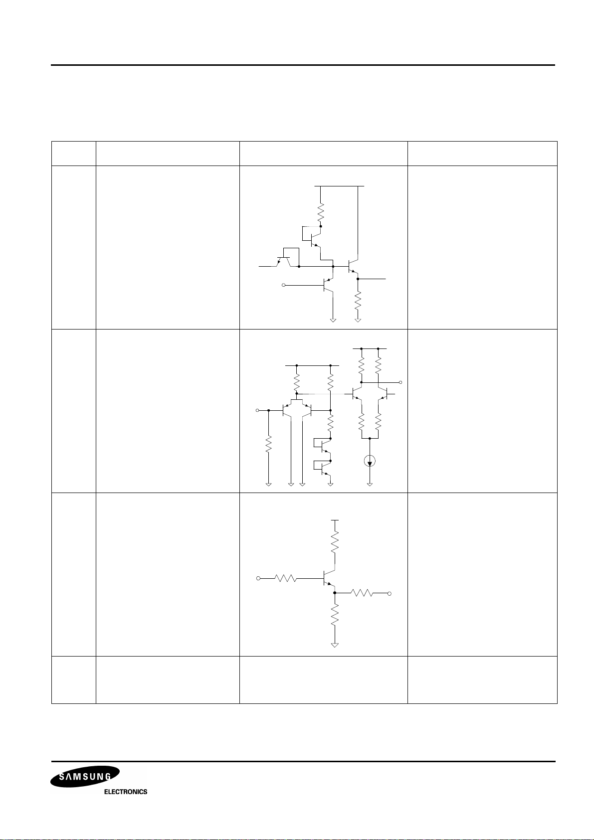
PIN DESCRIPTION
Table 2. Pin Description
Pin No Pin Name Schematic Description
1
Red OSD Input
(ROSD)
2
Green OSD Input
(GOSD)
3
Blue OSD Input
(BOSD)
4 Video/OSD Switch
(VI/OSD_SW)
1.29/
1.02V
PIN 4
PIN 1
VCC
VCC
OSD input signals are in TTL
level and will be connected to
ground when switching to
video input
1.16/
0.90V
Video/OSD switch signal is
6V
TTL level
PIN4 = “high”, OSD input
PIN4 = “Low”, video input
5
8
10
6
9
Red Video Input
(RIN)
Green Video Input
(GIN)
Blue Video Input
(BIN)
V
CC1
V
CC2
PIN 5
VCC
MAX input video signal is
0.7 Vpp
Supply voltage
-
(except drive part)
5
KA2500 I2C BUS CONTROLLED R/G/B VIDEO AMPLIFIER FOR MONITORS
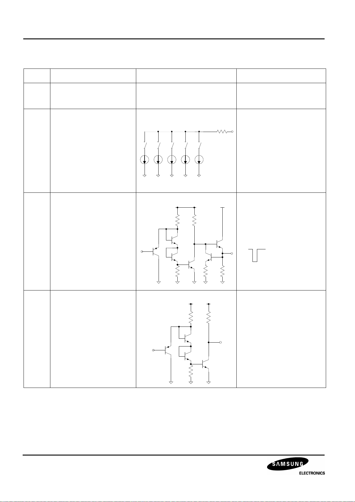
Table 2. Pin Description (Continued)
Pin No Pin Name Schematic Description
7
11
15
GND1
GND2 (GND (L) )
Blue Cut-Off
(BCT)
16
Green Cut-Off
(GCT)
17
Red Cut-Off
(RCT)
18 Clamp Gate Input
(CLP)
-
0~180uA 0~540uA 80uA 160uA 320uA
PIN 18
Cut-OffCut-Off
BRT
Cut-Off
Offset
5.1V
PIN 17
Ground (analogue)
Ground (logic)
Cut-Off Control Output
Video amp active when clamp
VCC
gate signal is in low TTL level.
Clamp gate Min. pulse width
: 0.2us, at fh: 50KHz
19 Blank Gate Input
(BLK)
PIN 19
6
7V VCC
Video amp blanks video signal
when blank gate signal is in
low TTL level.
I2C BUS CONTROLLED R/G/B VIDEO AMPLIFIER FOR MONITORS KA2500
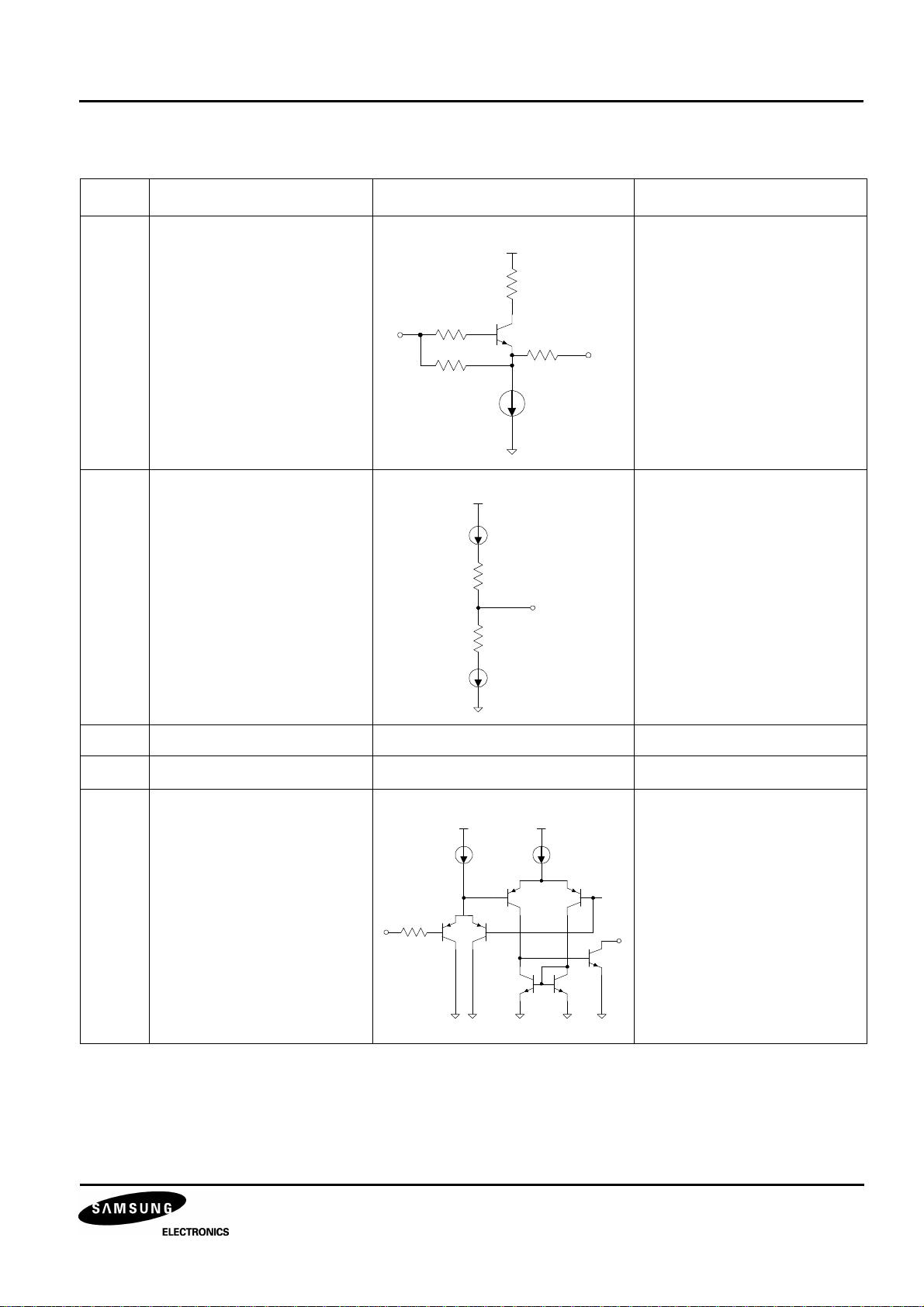
Table 2. Pin Description (Continued)
Pin No Pin Name Schematic Description
26
24
21
20
25
27
Red Video Output
(ROUT)
Green Video Output
(GOUT)
Blue Video Output
(BOUT)
Blue Clamp Cap
(BCLP)
Green Clamp Cap
(GCLP)
Red Clamp Cap
(RCLP)
VCC
Video signal output
PIN 26
Brightness control activated
by charging and discharging of
the external cap. (0.1µF)
(During low clamp gate)
PIN 27
22 GND3 - Ground (drive part)
23 V
13
14
CC3
SCL
SDA
- Supply voltage (drive part)
Serial clock input port of I2C
54uA 27uA
BUS
Serial data input port of I2C
BUS
3.22V
PIN 13
7
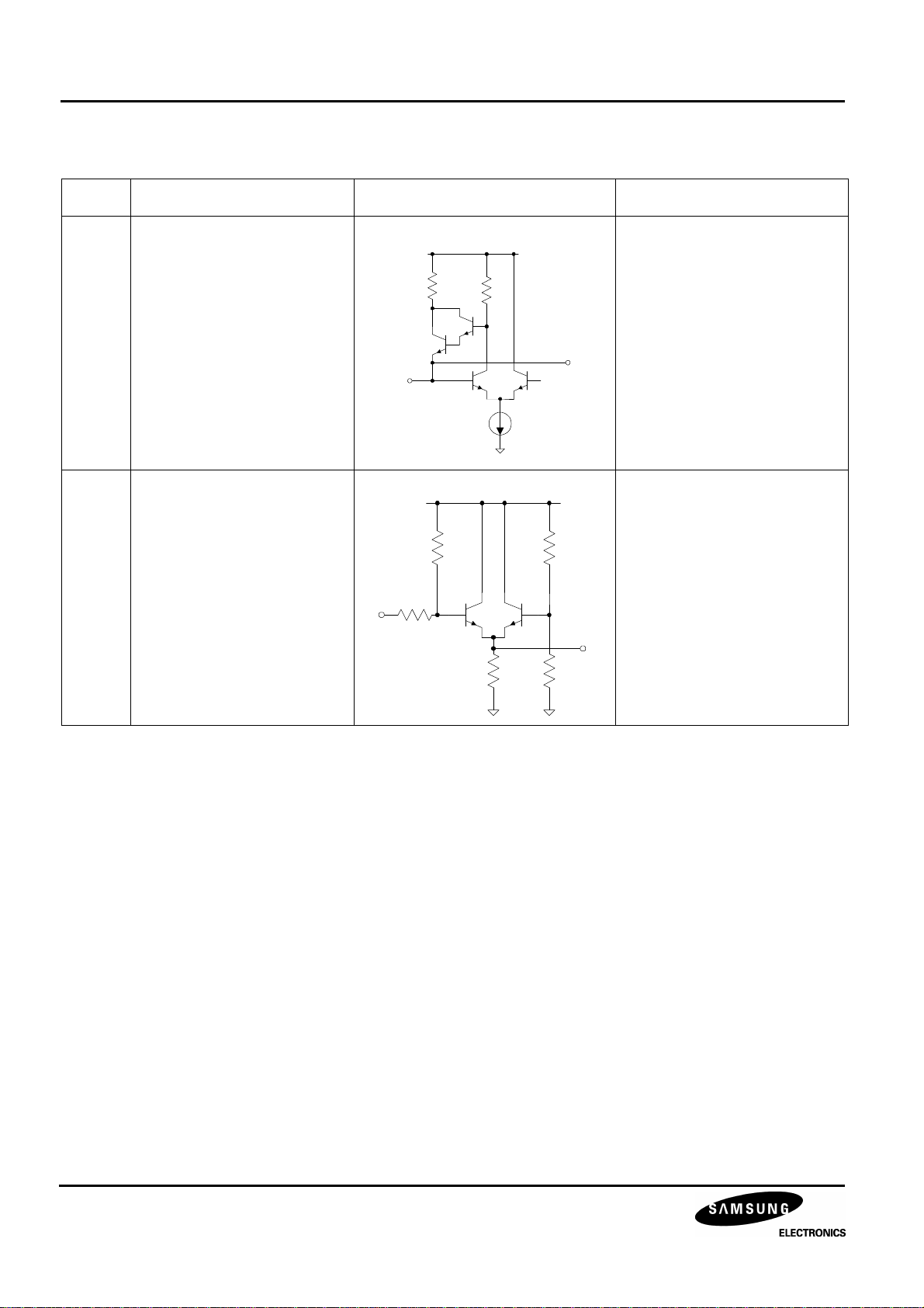
KA2500 I2C BUS CONTROLLED R/G/B VIDEO AMPLIFIER FOR MONITORS
Table 2. Pin Description (Continued)
Pin No Pin Name Schematic Description
28 B/U Input (B/U) Parabola input via AC coupling
VCC
cap
PIN 28
12 ABL Input (ABL) Automatic beam limitation
4.6V
100uA
VCC
input
(Control Range: 0.5 ~ 4.5V)
PIN 12
8
 Loading...