

Samsung KA348D, KA248, KA348, KA248D Datasheet
KA248/KA348 QUAD OPERATIONAL AMPLIFIER
QUAD OPERATIONAL AMPLIFIERS
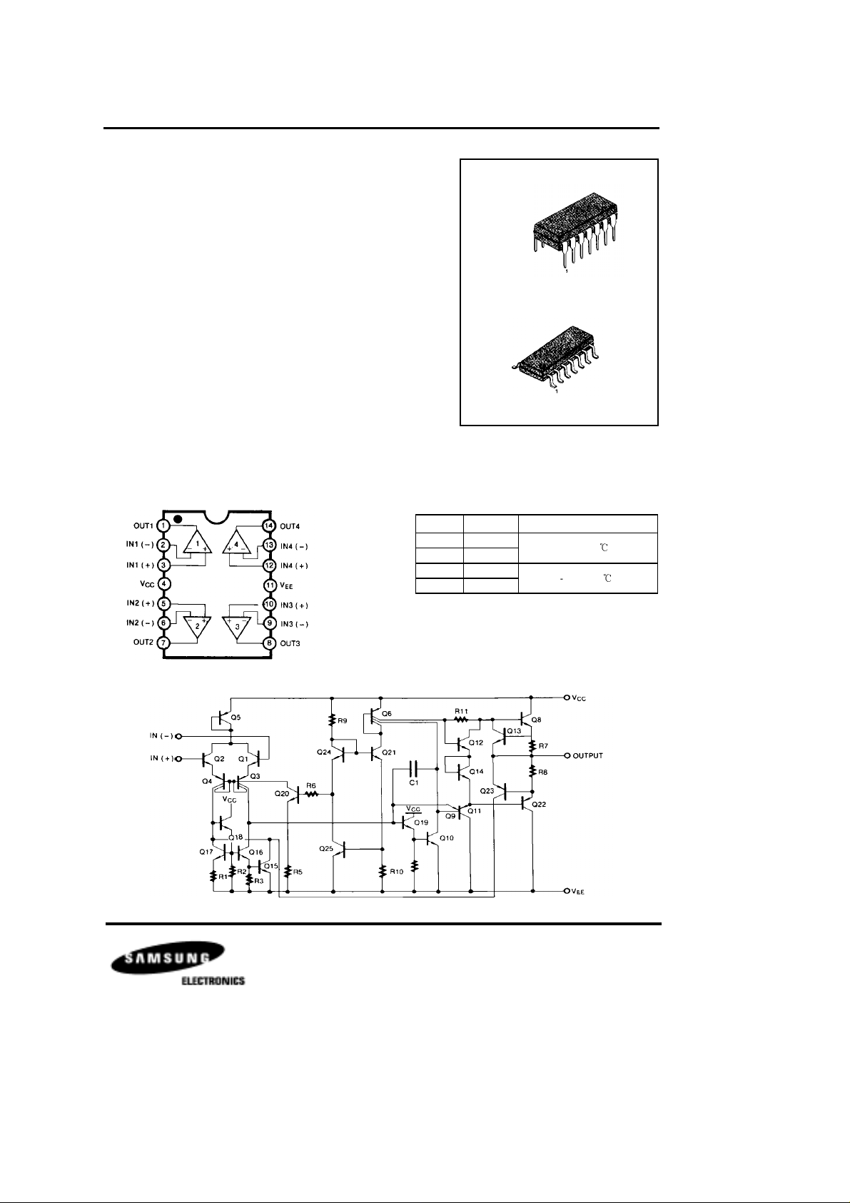
The KA248/KA348 is a true quad KA741. It consists of four independ- 14 DIP
ent, high-gain, internally compensated, low-power operational amplifiers
which have been designed to provide functional characteristics identical
to those of the familiar KA741
supply current for all four amplifiers is comparable to the Supply current
of a single KA741 type OP Amp.
Other features include input offset currents and input bias current which
are much less than those of a standard KA741. Also, excellent
between amplifiers has been
amplifier and using layout techniques
FEATURES
• KA741 OP Amp operating characteristics
• Low supply current drain
• Class AB output stage-no crossover distortion
• Pin compatible with the KA324 & KA3403
• Low input offset voltage- 1mV Type.
• Low input offset current-4nA Type.
• Low input bias current-30nA Type.
• Gain bandwidth product for KA348 (unity gain)-1.0MHz Type.
• High degree of isolation between amplifiers-120dB
• Overload protection for inputs and outputs
BLOCK DIAGRAM ORDERING INFORMATION
operational amplifier. In addition the total
isolation
achieved by independently biasing each
which minimize thermal coupling. 14 SOP
Device Package Operating Temperature
KA348 14 DIP
KA348D 14 SOP
KA248 14 DIP
KA248D 14 SOP
0 ~ +70
-25 ~ +85
Î
Î
SCHEMATIC DIAGRAM
(One Section Only)
KA248/KA348 QUAD OPERATIONAL AMPLIFIER
ABSOLUTE MAXIMUM RATINGS (TA = 25
ÎÎ)
Characteristic Symbol Value Unit
Supply Voltage
Differential Input Voltage
Input Voltage
Output Short Circuit Duration
Operating Temperature KA248
KA348
Storage Temperature
V
T
T
V
CC
I(DIFF)
V
I
OPR
STG
ä
18
ä
36
ä
18
Continuous
- 25 ~ +85
0~ +70
- 65~ +150
V
V
V
Î
Î
Î
ELECTRICAL CHARACTERISTICS
(VCC =15V, VEE= -15V, TA=25Î, unless otherwise specified)
Characteristic Symbol Test Conditions
RS'
10K
Input Offset Voltage
Input Offset Current
Input Bias Current
Input Resistance R
Supply Current (all Amplifiers) I
Large Signal Voltage Gain
G
V
I
I
IO
BIAS
CC
IO
I
V
`
NOTE 1 7.5 7.5
NOTE 1 125 100
NOTE 1 500 400
RL(2K`
NOTE 1 15 15
Channel Separation CS f = 1KHz to 20KHz 120 120 dB
Common Mode Input
Voltage Range
NOTE 1
V
I(R)
Small Signal Bandwidth BW GV = 1 1.0 1.0 MHz
Phase Margin MPH GV = 1 60 60 Degress
Slew Rate SR GV = 1 0.5 0.5
Output Short Circuit Current I
Output Voltage Swing
Common Mode Rejection Ratio CMRR
Power Supply Rejection Ratio PSRR
SC
RL(
10K
RL(2K`
(
10K
R
S
(
10K
R
S
`
NOTE 1V
NOTE 1 70 90 70 90 dB
`
NOTE 1 77 96 77 96 dB
`
KA248 KA348
Min Typ Max Min Typ Max
1 6.0 1 6.0
450 450
30 200 30 200
0.8 2.5 0.8 2.5
2.4 4.5 2.4 4.5 mA
25 160 25 160
ä
12
ä
12
25 25 mA
ä12ä
ä10ä
13
12
ä12ä
0ä
13
12
Unit
mV
nA
nA
M
`
V
V/ss
NOTE 1
KA348: 0 (T
KA248: -25 (T
(
+70
Î
A
(
+85
Î
A
KA248/KA348 QUAD OPERATIONAL AMPLIFIER
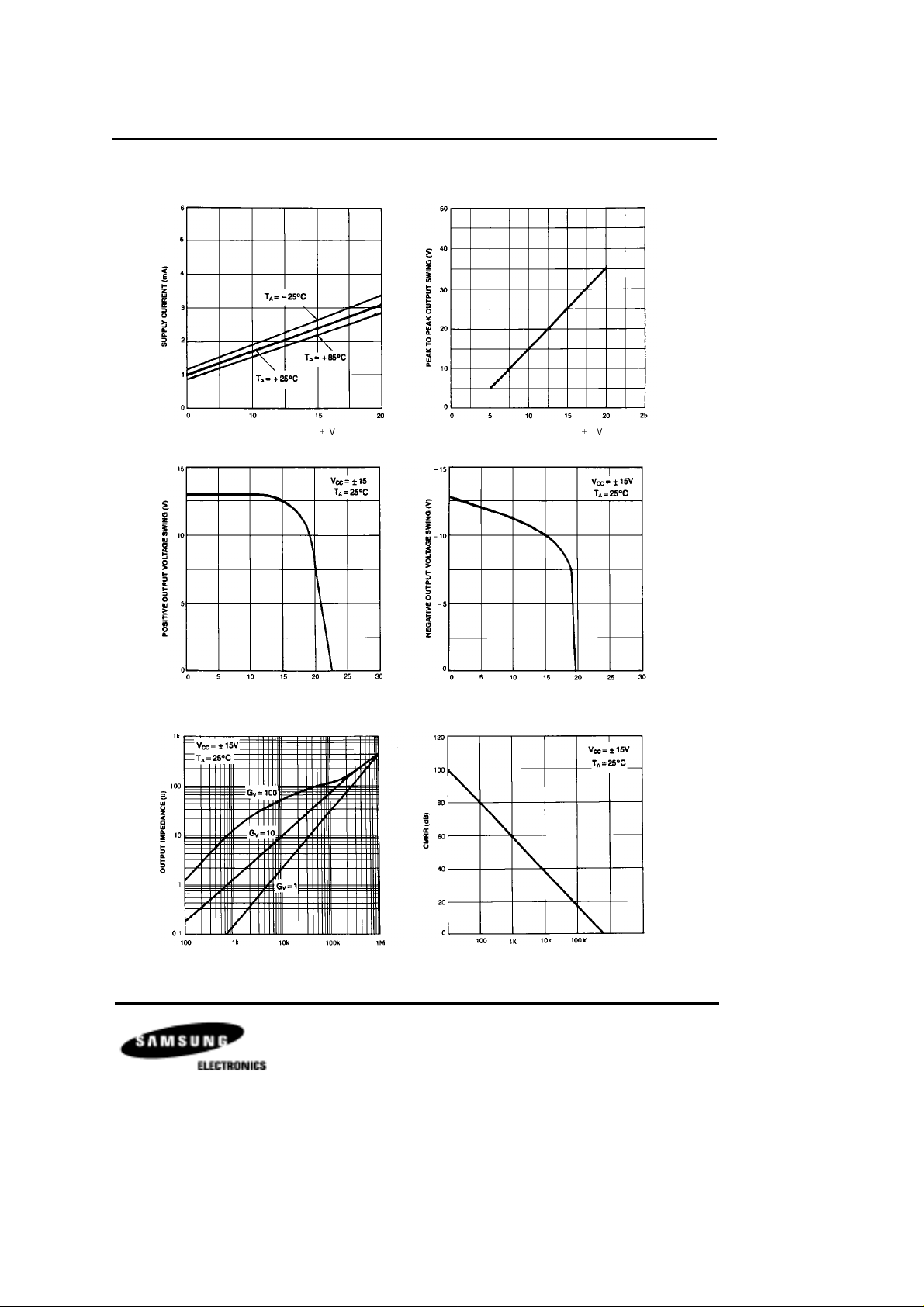
TYPICAL PERFORMANCE CHARACTERISTICS
Fig. 1 SUPPLY CURRENT Fig. 2 VOLTAGE SWING
SUPPLY VOLTAGE (äV) SUPPLY VOLTAGE (ä V)
Fig. 3 SOURCE CURRENT LIMIT Fig. 4 SINK CURRENT LIMIT
OUTPUT SOURCE CURRENT (mA) OUTPUT SINK CURRENT (mA)
FREQUENCY (HZ) FREQUENCY (Hz)
Fig. 5 OUTPUT IMPEDANCE Fig. 6 COMMON-MODE REJECTION RATIO
 Loading...