


现货库存、技术资料、百科信息、热点资讯,精彩尽在鼎好!
K9F1208U0C
K9F1208R0C
K9F1208B0C
K9F1208X0C
FLASH MEMORY
INFORMATION IN THIS DOCUMENT IS PROVIDED IN RELATION TO SAMSUNG PRODUCTS,
AND IS SUBJECT TO CHANGE WITHOUT NOTICE.
NOTHING IN THIS DOCUMENT SHALL BE CONSTRUED AS GRANTING ANY LICENSE,
EXPRESS OR IMPLIED, BY ESTOPPEL OR OTHERWISE,
TO ANY INTELLECTUAL PROPERTY RIGHTS IN SAMSUNG PRODUCTS OR TECHNOLOGY. ALL
INFORMATION IN THIS DOCUMENT IS PROVIDED
ON AS "AS IS" BASIS WITHOUT GUARANTEE OR WARRANTY OF ANY KIND.
1. For updates or additional information about Samsung products, contact your nearest Samsung office.
2. Samsung products are not intended for use in life support, critical care, medical, safety equipment, or similar
applications where Product failure could result in loss of life or personal or physical harm, or any military or
defense application, or any governmental procurement to which special terms or provisions may apply.
* Samsung Electronics reserves the right to change products or specification without notice.
1

K9F1208U0C
K9F1208R0C
K9F1208B0C
Document Title
64M x 8 Bits NAND Flash Memory
Revision History
FLASH MEMORY
Revision No.
0.0
0.1
0.2
0.3
0.4
0.5
1.0
1.1
History
Initial issue.
2.7V part is added
Address of Read 2 is changed (A
1. Add tRPS/tRCS/tREAS parameter for status read
2. Add nWP timing guide
1. Change from tRPS/tRCS/tREAS to tRPB/tRCB/tREAB parameter for
1.8V device busy state
1. Sequential Row Read is added
1. tCRY is changed (50ns+tR(R/B) --> 5us)
1. Mode selection is modified ("CE
: Don’t care -> Fixed "Low" )
4~A7
don’t care" case)
Draft Date
Nov. 10th 2005
July 13th 2006
Aug. 1st 2006
Oct. 12th 2006
Nov. 14th 2006
Nov. 15th 2006
Dec. 28th 2006
June 18th 2007
Remark
Advance
Advance
Advance
Advance
Advance
Preliminary
Final
Final
Note : For more detailed features and specifications including FAQ, please refer to Samsung’s Flash web site.
http://www.samsung.com/Products/Semiconductor/
The attached datasheets are prepared and approved by SAMSUNG Electronics. SAMSUNG Electronics CO., LTD. reserve the right
to change the specifications. SAMSUNG Electronics will evaluate and reply to your requests and questions about device. If you have
any questions, please contact the SAMSUNG branch office near you.
2

K9F1208U0C
K9F1208R0C
K9F1208B0C
64M x 8 Bits NAND Flash Memory
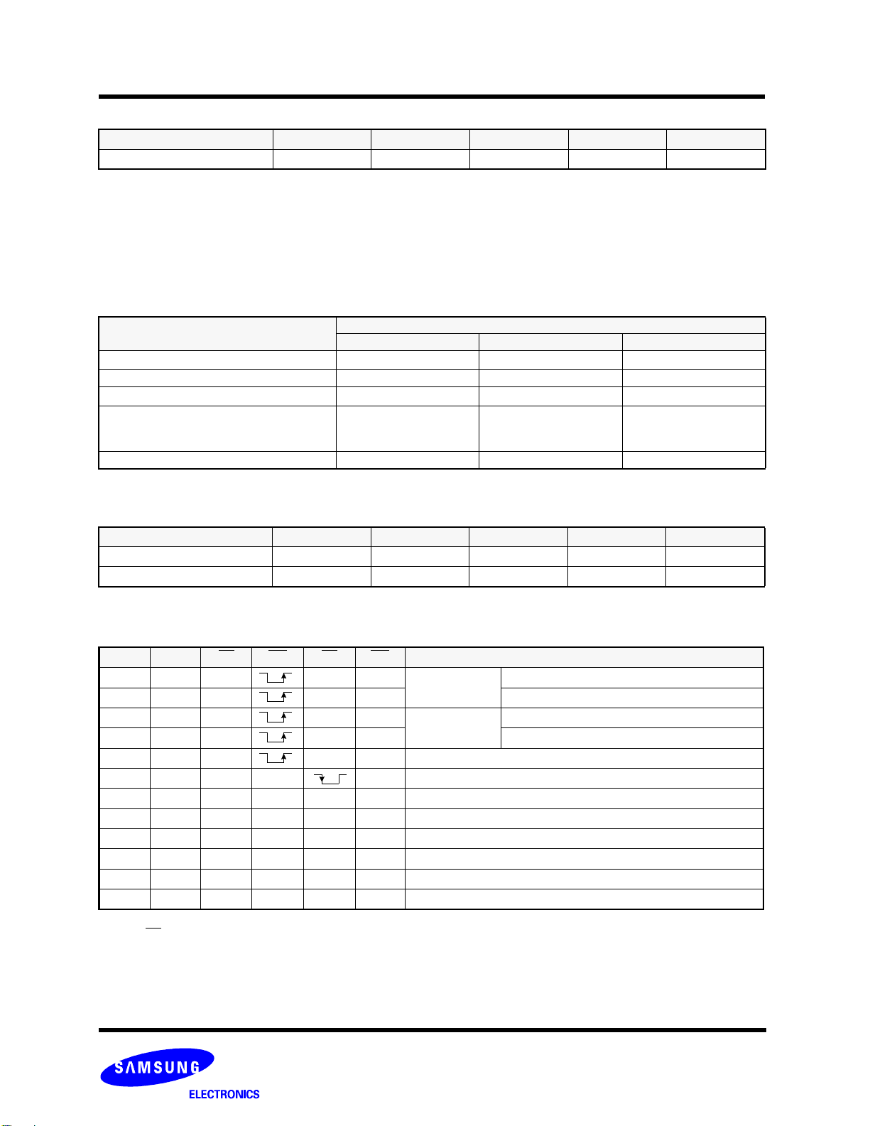
PRODUCT LIST
Part Number Vcc Range Organization PKG Type
K9F1208R0C-J 1.65V ~ 1.95V
K9F1208B0C-P 2.5V ~ 2.9V TSOP1
K9F1208U0C-P
K9F1208U0C-J FBGA
FEATURES
• Voltage Supply
- 1.8V Device(K9F1208R0C) : 1.65V ~ 1.95V
- 2.7V Device(K9F1208B0C) : 2.5V ~ 2.9V
- 3.3V Device(K9F1208U0C) : 2.7V ~ 3.6V
• Organization
- Memory Cell Array : (64M + 2M) x 8bits
- Data Register : (512 + 16) x 8bits
• Automatic Program and Erase
- Page Program : (512 + 16) x 8bits
- Block Erase : (16K + 512)Bytes
• Page Read Operation
- Page Size : (512 + 16)Bytes
- Random Access : 15µs(Max.)
- Serial Page Access : 42ns(Min.)
• Fast Write Cycle Time
- Program time : 200µs(Typ.)
- Block Erase Time : 2ms(Typ.)
• Command/Address/Data Multiplexed I/O Port
• Hardware Data Protection
- Program/Erase Lockout During Power Transitions
2.7V ~ 3.6V
FLASH MEMORY
FBGA
x8
TSOP1
• Reliable CMOS Floating-Gate Technology
- Endurance : 100K Program/Erase Cycles
(with 1bit/512Byte ECC)
- Data Retention : 10 Years
• Command Register Operation
• Unique ID for Copyright Protection
• Package
- K9F1208U0C-PCB0/PIB0 : Pb-Free Package
48 - Pin TSOP I (12 x 20 / 0.5 mm pitch)
- K9F1208X0C-JCB0/JIB0: Pb-Free Package
63-Ball FBGA(8.5 x 13 x 1.2mmt)
- K9F1208B0C-PCB0/PIB0 : Pb-Free Package
48 - Pin TSOP I (12 x 20 / 0.5 mm pitch)
GENERAL DESCRIPTION
Offered in 64Mx8bits, the K9F1208X0C is 512Mbit with spare 16Mbit capacity. The device is offered in 1.8V, 2.7V and 3.3V Vcc. Its
NAND cell provides the most cost-effective solutIon for the solid state mass storage market. A program operation can be performed in
typical 200µs on the 528-bytes and an erase operation can be performed in typical 2ms on a 16K-bytes block. Data in the page can
be read out at 42ns cycle time per byte. The I/O pins serve as the ports for address and data input/output as well as command input.
The on-chip write control automates all program and erase functions including pulse repetition, where required, and internal verification and margining of data. Even the write-intensive systems can take advantage of the K9F1208X0C′s extended reliability of 100K
program/erase cycles by providing ECC(Error Correcting Code) with real time mapping-out algorithm.
The K9F1208X0C is an optimum solution for large nonvolatile storage applications such as solid state file storage and other portable
applications requiring non-volatility.
3
K9F1208U0C
K9F1208R0C
PIN CONFIGURATION (TSOP1)
K9F1208B0C
FLASH MEMORY
K9F1208X0C-PCB0/PIB0
N.C
N.C
N.C
N.C
N.C
N.C
R/B
RE
CE
N.C
N.C
Vcc
Vss
N.C
N.C
CLE
ALE
WE
WP
N.C
N.C
N.C
N.C
N.C
1
2
3
4
5
6
7
8
9
10
11
12
13
14
15
16
17
18
19
20
21
22
23
24
48
47
46
45
44
43
42
41
40
39
38
37
36
35
34
33
32
31
30
29
28
27
26
25
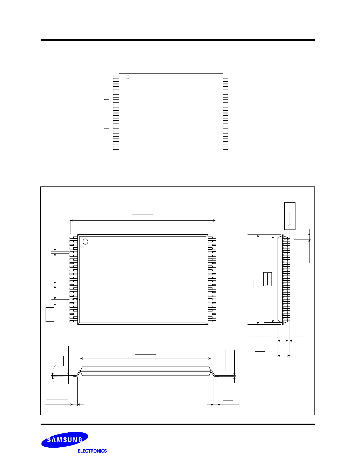
PACKAGE DIMENSIONS
48-PIN LEAD/LEAD FREE PLASTIC THIN SMALL OUT-LINE PACKAGE TYPE(I)
48 - TSOP1 - 1220AF
20.00±0.20
0.787±0.008
+0.07
-0.03
#1
0.20
#48
N.C
N.C
N.C
N.C
I/O7
I/O6
I/O5
I/O4
N.C
N.C
N.C
Vcc
Vss
N.C
N.C
N.C
I/O3
I/O2
I/O1
I/O0
N.C
N.C
N.C
N.C
Unit :mm/Inch
MAX
0.10
0.004
0.25
()
0.010
+0.003
-0.001
+0.07
-0.03
0.16
0.008
0.50
0.0197
0~8°
0.45~0.75
0.018~0.030
#24
0.25
MAX
12.00
0.472
0.488
12.40
#25
1.00±0.05
0.039±0.002
1.20
TYP
0.010
18.40±0.10
0.724±0.004
+0.075
0.035
+0.003
-0.001
0.125
0.005
0.50
()
0.020
0.047
MAX
0.05
0.002
MIN
4
K9F1208U0C
K9F1208R0C
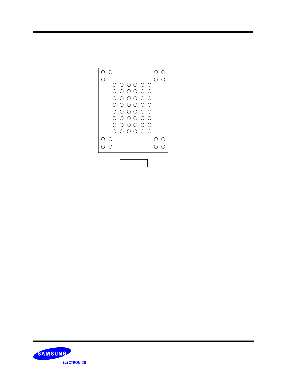
PIN CONFIGURATION (FBGA)
K9F1208B0C
FLASH MEMORY
K9F1208X0C-JCB0/JIB0
3456 1 2
A
B
C
D
E
F
G
H
N.C N.C
N.C
N.C N.C
N.C
/RE CLE
NC
NC
NC
NC NC
NC NC NC
NC NC
NC
NC
NCNCNC
NC NC
NCNC I/O0
I/O1NC NC VccQ I/O5 I/O7
Top View
N.C N.C
N.C
N.C
R/B/WE/CEVssALE/WP
NC
NC
NC
NC
NCNC
NC
Vcc
VssI/O6I/O4I/O3I/O2Vss
N.C N.C
N.C
N.CN.C
5
K9F1208U0C
K9F1208R0C
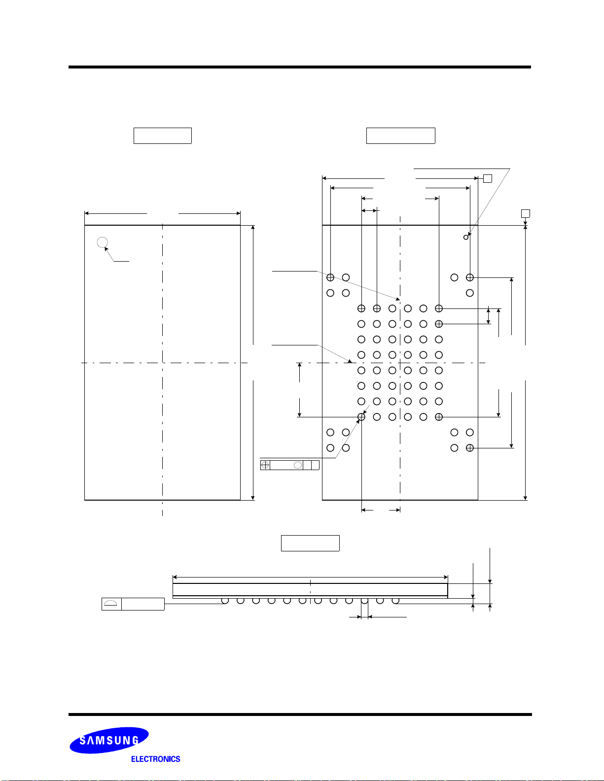
63-Ball FBGA (measured in millimeters)
K9F1208B0C
FLASH MEMORY
#A1
Top View
8.50±0.10
13.00±0.10
(Datum A)
(Datum B)
2.80
Bottom View
#A1 INDEX MARK(OPTIONAL)
8.50±0.10
0.80 x 9= 7.20
0.80 x 5= 4.00
0.80
65
A
B
C
D
E
F
G
H
4321
A
0.80
0.80 x 7= 5.60
B
13.00±0.10
0.80 x 11= 8.80
0.10MAX
63-∅0.45±0.05
∅
0.20
M
A B
Side View
13.00±0.10
2.00
0.45±0.05
0.90±0.10
0.35±0.05
6

K9F1208U0C
K9F1208R0C
PIN DESCRIPTION
Pin Name Pin Function
0 ~ I/O7
I/O
CLE
ALE
CE
RE
WE
K9F1208B0C
DATA INPUTS/OUTPUTS
The I/O pins are used to input command, address and data, and to output data during read operations. The I/
O pins float to high-z when the chip is deselected or when the outputs are disabled.
COMMAND LATCH ENABLE
The CLE input controls the activating path for commands sent to the command register. When active high,
commands are latched into the command register through the I/O ports on the rising edge of the WE
ADDRESS LATCH ENABLE
The ALE input controls the activating path for address to the internal address registers. Addresses are
latched on the rising edge of WE
CHIP ENABLE
The CE
input is the device selection control. When the device is in the Busy state, CE high is ignored, and
the device does not return to standby mode in program or erase opertion. Regarding CE
operation, refer to ’Page read’ section of Device operation .
READ ENABLE
The RE
input is the serial data-out control, and when active drives the data onto the I/O bus. Data is valid
tREA after the falling edge of RE
WRITE ENABLE
The WE
input controls writes to the I/O port. Commands, address and data are latched on the rising edge of
the WE
pulse.
with ALE high.
which also increments the internal column address counter by one.
FLASH MEMORY
signal.
control during read
WRITE PROTECT
The WP
WP
R/B
Vcc
Vss GROUND
N.C
DNU
NOTE : Connect all VCC and VSS pins of each device to common power supply outputs.
pin provides inadvertent write/erase protection during power transitions. The internal high voltage
generator is reset when the WP
READY/BUSY OUTPUT
The R/B
output indicates the status of the device operation. When low, it indicates that a program, erase or
random read operation is in process and returns to high state upon completion. It is an open drain output and
does not float to high-z condition when the chip is deselected or when outputs are disabled.
POWER
V
CC is the power supply for device.
NO CONNECTION
Lead is not internally connected.
DO NOT USE
Leave it disconnected.
pin is active low.
Do not leave VCC or VSS disconnected.
7
K9F1208U0C
K9F1208R0C
Figure 1. K9F1208X0C FUNCTIONAL BLOCK DIAGRAM
VCC
SS
V
K9F1208B0C
FLASH MEMORY
A9 - A25
A0 - A7
X-Buffers
Latches
& Decoders
Y-Buffers
Latches
& Decoders
A8
Command
Command
Register
CE
RE
WE
Control Logic
& High Voltage
Generator
CLE ALE
WP
Figure 2. K9F1208X0C ARRAY ORGANIZATION
512M + 16M Bits
NAND Flash
ARRAY
(512 + 16)Bytes x 131,072
Page Register & S/A
Y-Gat ing
I/O Buffers & Latches
Global Buffers
1 Block = 32 Pages
= (16K + 512) Bytes
Output
Driver
VCC
VSS
I/0 0
I/0 7
128K Pages
(=4,096 Blocks)
1st Cycle A
2nd Cycle A9 A10 A11 A12 A13 A14 A15 A16
3rd Cycle A17 A18 A19 A20 A21 A22 A23 A24
4th Cycle A25 *L *L *L *L *L *L *L
NOTE : Column Address : Starting Address of the Register.
1st half Page Register
(=256 Bytes)
512Bytes 16 Bytes
I/O 0 I/O 1 I/O 2 I/O 3 I/O 4 I/O 5 I/O 6 I/O 7
0 A1 A2 A3 A4 A5 A6 A7
00h Command(Read) : Defines the starting address of the 1st half of the register.
01h Command(Read) : Defines the starting address of the 2nd half of the register.
8 is set to "Low" or "High" by the 00h or 01h Command.
* A
* L must be set to "Low".
* The device ignores any additional input of address cycles than reguired.
2nd half Page Register
(=256 Bytes)
Page Register
512 Bytes
8 bits
I/O 0 ~ I/O 7
16 Bytes
1 Page = 528 Bytes
1 Block = 528 Bytes x 32 Pages
= (16K + 512) Bytes
1 Device = 528Bytes x 32Pages x 4,096 Blocks
= 528 Mbits
Column Address
Row Address
(Page Address)
8
K9F1208U0C
K9F1208R0C
Product Introduction
The K9F1208X0C is a 528Mbits(553,648,218 bits) memory organized as 131,072 rows(pages) by 528 columns. Spare sixteen columns are located from column address of 512 to 527. A 528-bytes data register is connected to memory cell arrays accommodating
data transfer between the I/O buffers and memory during page read and page program operations. The memory array is made up of
16 cells that are serially connected to form a NAND structure. Each of the 16 cells resides in a different page. A block consists of the
32 pages formed two NAND structures. A NAND structure consists of 16 cells. Total 135,168 NAND structures reside in a block. The
program and read operations are executed on a page basis, while the erase operation is executed on a block basis. The memory
array consists of 4,096 separately erasable 16K-bytes blocks. It indicates that the bit by bit erase operation is prohibited on the
K9F1208X0C.
The K9F1208X0C has addresses multiplexed into 8 I/O's. This scheme dramatically reduces pin counts and allows systems
upgrades to future densities by maintaining consistency in system board design. Command, address and data are all written through
I/O's by bringing WE
Latch Enable(ALE) are used to multiplex command and address respectively, via the I/O pins. The 64M byte physical space requires
26 addresses, thereby requiring four cycles for byte-level addressing : 1 cycle of column address, 3 cycles of row address, in that
order. Page Read and Page Program need the same four address cycles following the required command input. In Block Erase operation, however, only the 3 cycles of row address are used. Device operations are selected by writing specific commands into the
command register. Table 1 defines the specific commands of the K9F1208X0C.
Table 1. Command Sets
Read 1
Read 2 50h -
Read ID 90h -
Reset FFh - O
Page Program 80h 10h
Block Erase 60h D0h
Block Protect 1 41h -
Block Protect 2 42h -
Block Protect 3 43h -
Read Status 70h - O
Read Protection Status 7Ah -
NOTE : 1. The 00h/01h command defines starting address of the 1st/2nd half of registers.
After data access on the 2nd half of register by the 01h command, the status pointer is automatically moved to the 1st half register(00h)
on the next cycle.
Caution : Any undefined command inputs are prohibited except for above command set of Table 1.
K9F1208B0C
to low while CE is low. Data is latched on the rising edge of WE. Command Latch Enable(CLE) and Address
Function 1’st Cycle 2’nd Cycle
00h/01h
(1)
-
FLASH MEMORY
Acceptable Command
during Busy
9

K9F1208U0C
K9F1208R0C
ABSOLUTE MAXIMUM RATINGS
Voltage on any pin relative to VSS
Temperature Under
Bias
Storage Temperature
Short Circuit Current
NOTE :
1. Minimum DC voltage is -0.6V on input/output pins. During transitions, this level may undershoot to -2.0V for periods <30ns.
Maximum DC voltage on input/output pins is V
2. Permanent device damage may occur if ABSOLUTE MAXIMUM RATINGS are exceeded. Functional operation should be restricted to the conditions
as detailed in the operational sections of this data sheet. Exposure to absolute maximum rating conditions for extended periods may affect reliability.
RECOMMENDED OPERATING CONDITIONS
(Voltage reference to GND at the condision of K9F1208X0C-XCB0 : TA=0 to 70°C or K9F1208X0C-XIB0 : TA=-40 to 85°C)
Parameter Symbol
Supply Voltage
K9F1208B0C
Parameter Symbol
V
CC -0.6 to + 2.45 -0.6 to + 4.6
V
IN -0.6 to + 2.45 -0.6 to + 4.6
I/O -0.6 to Vcc + 0.3 (< 2.45V) -0.6 to Vcc + 0.3 (< 4.6V)
V
K9F1208X0C-XCB0
K9F1208X0C-XIB0 -40 to +125
K9F1208X0C-XCB0
K9F1208X0C-XIB0
CC+0.3V which, during transitions, may overshoot to VCC+2.0V for periods <20ns.
BIAS
T
T
STG -65 to +150 °C
IOS 5mA
1.8V(K9F1208R0C)
1.8V Device 2.7V/3.3V Device
2.7V(K9F1208B0C)
Rating
-10 to +125
FLASH MEMORY
3.3V(K9F1208U0C)
Min Typ . Max Min Typ. Max Min Typ. Max
CC 1.65 1.8 1.95 2.5 2.7 2.9 2.7 3.3 3.6 V
V
SS 0000 0 0000V
V
Unit
V
°C
Unit
DC AND OPERATING CHARACTERISTICS (Recommended operating conditions otherwise noted.)
K9F1208X0C
Parameter Symbol Test Conditions
Operating
Current
Sequential
Read
ICC1
tRC=42ns, CE
=0mA
I
OUT
Program ICC2 - - 8 20 - 10 20 - 10 20
=VIL,
Erase ICC3 - - 8 20 - 10 20 - 10 20
=VIH, WP=0V/V
Stand-by Current(TTL) ISB1
Stand-by Current(CMOS) ISB2
Input Leakage Current
Output Leakage Current
Input High Voltage
Input Low Voltage, All inputs
CE
CE
VIN=0 to Vcc(max)
I
LI
I
V
LO
V
IH
V
IL
=VCC-0.2, WP=0V/V
=0 to Vcc(max)
OUT
- -0.3 - 0.4 -0.3 - 0.5 -0.3 - 0.8
CC
K9F1208R0C: IOH=-100µA
Output High Voltage Level
K9F1208B0C: I
OH
K9F1208U0C: I
=-100µA
OH
=-400µA
OH
V
K9F1208R0C: IOL=100µA
V
Output Low Voltage Level
K9F1208B0C: I
OL
K9F1208U0C: I
(R/B)VOL=0.4V
Output Low Current(R/B
Notes :
1. Typical values are measured at Vcc=3.3V, TA=25°C. And not 100% tested.
I
)
OL
=100µA
OL
=2.1mA
OL
CC
1.8V 2.7V 3.3V
Min Typ Max Min Typ Max Min Typ Max
- 8 20 - 10 20 - 10 20
--1 - -1--1
-1050 - 1050 -1050
--±10 - - ±10 - - ±10
--±10 - - ±10 - - ±10
V
CC
-0.4
V
CC
-0.1
V
CC
+0.3
--
V
CC
-0.4
V
CC
-0.4
V
CC
+0.3
2.0 -
--2.4--
V
+0.
- - 0.1 - - 0.4 - - 0.4
34- 34- 810-mA
Uni
t
mA
µA
CC
3
V
10
K9F1208U0C
K9F1208R0C
VALID BLOCK
Parameter Symbol Min Typ. Max Unit
Valid Block Number N
NOTE :
1. The K9F1208X0C may include invalid blocks when first shipped. Additional invalid blocks may develop while being used. The number of valid blocks
is presented with both cases of invalid blocks considered. Invalid blocks are defined as blocks that contain one or more bad bits. Do not erase or
program factory-marked bad blocks. Refer to the attached technical notes for a appropriate management of invalid blocks.
2. The 1st block, which is placed on 00h block address, is guaranteed to be a valid block up to 1K program/erase cycles with 1bit/512Byte ECC.
3. Minimum 1,004 valid blocks are guaranteed for each contiguous 128Mb memory space.
AC TEST CONDITION
(K9F1208X0C-XCB0 :TA=0 to 70°C, K9F1208X0C-XIB0:TA=-40 to 85°C).
Input Pulse Levels
Input Rise and Fall Times 5ns 5ns 5ns
Input and Output Timing Levels
K9F1208R0C:Output Load (Vcc:1.8V +/-10%)
K9F1208B0C:Output Load (Vcc:2.7V +/-10%)
K9F1208U0C:Output Load (Vcc:3.3V +/-10%)
K9F1208U0C:Output Load (Vcc:3.0V +/-10%) - - 1 TTL GATE and CL=50pF
K9F1208B0C
Parameter
FLASH MEMORY
VB 4,026 - 4,096 Blocks
Value
K9F1208R0C K9F1208B0C K9F1208U0C
0V to V
CC
/2
V
CC
1 TTL GATE and CL=30pF 1 TTL GATE and CL=30pF
0V to Vcc 0.4V to 2.4V
Vcc/2 1.5V
1 TTL GATE and
CL=100pF
CAPACITANCE(TA=25°C, VCC=1.8V/2.7V/3.3V, f=1.0MHz)
Item Symbol Test Condition Min Max Unit
Input/Output Capacitance C
Input Capacitance C
NOTE : Capacitance is periodically sampled and not 100% tested.
I/O VIL=0V - 10 pF
IN VIN=0V - 10 pF
MODE SELECTION
CLE ALE CE WE RE WP Mode
HLL HX
L H L H X Address Input (4 clocks)
HLL HH
L H L H H Address Input (4 clocks)
L L L H H Data Input
L L L H X Data Output
L L L H H X During Read (Busy) on K9F1208X0C_P
X X X X H X During Read (Busy) except on K9F1208X0C_P
X X X X X H During Program (Busy)
X X X X X H During Erase (Busy)
X
XXHXX
NOTE : 1. X can be VIL or VIH.
(1)
X
2. WP should be biased to CMOS high or CMOS low for standby.
X X X L Write Protect
0V/V
CC
(2)
Stand-by
Read Mode
Write Mode
Command Input
Command Input
11
K9F1208U0C
K9F1208R0C
Program / Erase Characteristics
Program Time
Number of Partial Program Cycles
in the Same Page
Block Erase Time t
NOTE NOTE: 1.Typical Program time is defined as the time within which more than 50% of the whole pages are programmed at Vcc of 3.3V and 25’C
AC TIMING CHARACTERISTICS FOR COMMAND / ADDRESS / DATA INPUT
CLE setup Time t
CLE Hold Time t
CE
setup Time tCS 31 - ns
CE
Hold Time tCH 5-ns
WE
Pulse Width
ALE setup Time t
ALE Hold Time t
Data setup Time t
Data Hold Time t
Write Cycle Time t
WE
High Hold Time tWH 15 - ns
K9F1208B0C
Parameter Symbol Min Typ Max Unit
(1)
PROG
t
Main Array
Spare Array - - 2 cycle
Parameter Symbol Min Max Unit
Nop
BERS -23ms
- 200 500 µs
--1cycle
CLS 21 - ns
CLH 5-ns
(1)
WP
t
ALS 21 - ns
ALH 5-ns
DS 20 - ns
DH 5-ns
WC 42 - ns
FLASH MEMORY
21 - ns
NOTE: The transition of the corresponding control pins must occur only once while WE is held low.
12
K9F1208U0C
K9F1208R0C
AC CHARACTERISTICS FOR OPERATION
Data Transfer from Cell to Register t
ALE to RE
CLE to RE
Ready to RE
RE Pulse Width t
WE High to Busy t
Read Cycle Time t
RE
CE
RE
CE
CE
RE
RE
Output Hi-Z to RE
WE
Device resetting time(Read/Program/Erase) t
RE Pulse Width during Busy State
Read Cycle Time during Busy State
RE
Delay tAR 10 - ns
Delay tCLR 10 - ns
Low tRR 20 - ns
Access Time tREA -30ns
Access Time tCEA -35ns
High to Output Hi-Z tRHZ -30ns
High to Output Hi-Z tCHZ -20ns
High to ALE or CLE Don’t Care tCSD 10 - ns
or CE High to Output hold tOH 15 - ns
High Hold Time tREH 15 - ns
High to RE Low tWHR 60 - ns
Access Time during Busy State
K9F1208B0C
FLASH MEMORY
Parameter Symbol Min Max Unit
R -15µs
RP 21 - ns
WB -100ns
RC 42 - ns
Low tIR 0-ns
RST -
(2)
t
RPB
(2)
t
RCB
(2)
REAB
t
5/10/500
35 - ns
50 - ns
-40ns
(1)
µs
Parameter Symbol Min Max Uni
Last RE High to Busy(at sequential read) t
K9F1208X0C-P only
NOTE: 1. If reset command(FFh) is written at Ready state, the device goes into Busy for maximum 5us.
2. This parameter (
3. The time to Ready depends on the value of the pull-up resistor tied R/B pin.
CE
High to Ready(in case of interception by CE at read) tCRY -
CE
High Hold Time(at the last serial read)
(4)
tRPB/tRCB/tREAB) must be used only for 1.8V device.
RB -100ns
5
µs
tCEH 100 - ns
13

K9F1208U0C
K9F1208R0C
NAND Flash Technical Notes
Initial Invalid Block(s)
Initial invalid blocks are defined as blocks that contain one or more initial invalid bits whose reliability is not guaranteed by Samsung.
The information regarding the initial invalid block(s) is so called as the initial invalid block information. Devices with initial invalid
block(s) have the same quality level as devices with all valid blocks and have the same AC and DC characteristics. An initial invalid
block(s) does not affect the performance of valid block(s) because it is isolated from the bit line and the common source line by a
select transistor. The system design must be able to mask out the initial invalid block(s) via address mapping. The 1st block, which is
placed on 00h block address, is guaranteed to be a valid block up to 1K program/erase cycles with 1bit
Identifying Initial Invalid Block(s)
All device locations are erased(FFh) except locations where the initial invalid block(s) information is written prior to shipping. The
initial invalid block(s) status is defined by the 6th byte in the spare area. Samsung makes sure that either the 1st or 2nd page of
every initial invalid block has non-FFh data at the column address of 517. Since the initial invalid block information is also erasable
in most cases, it is impossible to recover the information once it has been erased. Therefore, the system must be able to recognize
the initial invalid block(s) based on the initial invalid block information and create the initial invalid block table via the following suggested flow chart(Figure 3). Any intentional erasure of the initial invalid block information is prohibited.
K9F1208B0C
FLASH MEMORY
/512Byte ECC.
Start
Increment Block Address
Create (or update)
Initial Invalid Block(s) Table
Set Block Address = 0
Check "FFh" at the column address 517
*
No
No
Figure 3. Flow chart to create initial invalid block table.
Check "FFh" ?
Yes
Last Block ?
Yes
End
of the 1st and 2nd page in the block
14

K9F1208U0C
K9F1208R0C
NAND Flash Technical Notes (Continued)
Error in write or read operation
Within its life time, the additional invalid blocks may develop with NAND Flash memory. Refer to the qualification report for the block
failure rate.The following possible failure modes should be considered to implement a highly reliable system. In the case of status
read failure after erase or program, block replacement should be done. Because program status fail during a page program does not
affect the data of the other pages in the same block, block replacement can be executed with a page-sized buffer by finding an
erased empty block and reprogramming the current target data and copying the rest of the replaced block. In case of Read, ECC
must be employed. To improve the efficiency of memory space, it is recommended that the read failure due to single bit error should
be reclaimed by ECC without any block replacement. The block failure rate in the qualification report does not include those
reclaimed blocks.
Write
Read Single Bit Failure Verify ECC -> ECC Correction
K9F1208B0C
Failure Mode Detection and Countermeasure sequence
Erase Failure Status Read after Erase --> Block Replacement
Program Failure Status Read after Program --> Block Replacement
FLASH MEMORY
ECC
Program Flow Chart
: Error Correcting Code --> Hamming Code etc.
Example) 1bit correction & 2bits detection
Start
Write 80h
Write Address
Write Data
Write 10h
Read Status Register
I/O 6 = 1 ?
or R/B = 1 ?
No
*
Program Error
No
I/O 0 = 0 ?
Program Completed
Yes
Yes
: If program operation results in an error, map out
*
the block including the page in error and copy the
target data to another block.
15

K9F1208U0C
K9F1208R0C
NAND Flash Technical Notes (Continued)
K9F1208B0C
FLASH MEMORY
Erase Flow Chart
*
Erase Error
No
Start
Write 60h
Write Block Address
Write D0h
Read Status Register
I/O 6 = 1 ?
or R/B = 1 ?
Yes
I/O 0 = 0 ?
Yes
No
Read Flow Chart
Reclaim the Error
Start
Write 00h
Write Address
Read Data
ECC Generation
No
Verify ECC
Yes
Page Read Completed
Erase Completed
: If erase operation results in an error, map out
*
the failing block and replace it with another block.
Block Replacement
Block A
1st
∼
{
(n-1)th
nth
(page)
1st
∼
(n-1)th
nth
(page)
* Step1. When an error happens in the nth page of the Block ’A’ during erase or program operation.
* Step2. Copy the nth page data of the Block ’A’ in the buffer memory to the nth page of another free block. (Block ’B’)
* Step3. Then, copy the data in the 1st ~ (n-1)th page to the same location of the Block ’B’.
* Step4. Do not further erase Block ’A’ by creating an ’invalid Block’ table or other appropriate scheme.
an error occurs.
Block B
{
2
Buffer memory of the controller.
1
16

K9F1208U0C
K9F1208R0C
Pointer Operation of K9F1208X0C
Samsung NAND Flash has three address pointer commands as a substitute for the two most significant column addresses. ’00h’
command sets the pointer to ’A’ area(0~255byte), ’01h’ command sets the pointer to ’B’ area(256~511byte), and ’50h’ command sets
the pointer to ’C’ area(512~527byte). With these commands, the starting column address can be set to any of a whole
page(0~527byte). ’00h’ or ’50h’ is sustained until another address pointer command is inputted. ’01h’ command, however, is effective
only for one operation. After any operation of Read, Program, Erase, Reset, Power_Up is executed once with ’01h’ command, the
address pointer returns to ’A’ area by itself. To program data starting from ’A’ or ’C’ area, ’00h’ or ’50h’ command must be inputted
before ’80h’ command is written. A complete read operation prior to ’80h’ command is not necessary. To program data starting from
’B’ area, ’01h’ command must be inputted right before ’80h’ command is written.
K9F1208B0C
FLASH MEMORY
Table 2. Destination of the pointer
Command Pointer position Area
00h
01h
50h
0 ~ 255 byte
256 ~ 511 byte
512 ~ 527 byte
1st half array(A)
2nd half array(B)
spare array(C)
(1) Command input sequence for programming ’A’ area
The address pointer is set to ’A’ area(0~255), and sustained
Address / Data input
00h
’A’,’B’,’C’ area can be programmed.
It depends on how many data are inputted.
80h 10h 00h 80h 10h
"A" area
(00h plane)
256 Bytes
"A" "B" "C"
Pointer select
commnad
(00h, 01h, 50h)
"B" area
(01h plane)
256 Bytes
Pointer
"C" area
(50h plane)
16 Bytes
Figure 4. Block Diagram of Pointer Operation
Address / Data input
’00h’ command can be omitted.
Internal
Page Register
(2) Command input sequence for programming ’B’ area
The address pointer is set to ’B’ area(256~511), and will be reset to
’A’ area after every program operation is executed.
Address / Data input
01h
’B’, ’C’ area can be programmed.
It depends on how many data are inputted.
80h 10h 01h 80h 10h
(3) Command input sequence for programming ’C’ area
The address pointer is set to ’C’ area(512~527), and sustained
Address / Data input
50h
Only ’C’ area can be programmed.
80h 10h 50h 80h 10h
17
Address / Data input
’01h’ command must be rewritten before
every program operation
Address / Data input
’50h’ command can be omitted.

K9F1208U0C
K9F1208R0C
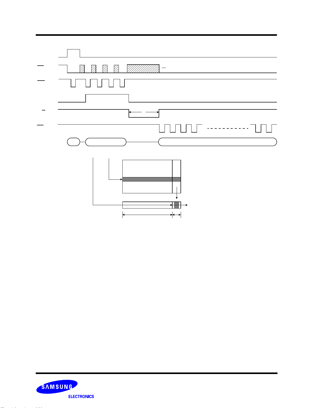
System Interface Using CE don’t-care.
For an easier system interface, CE may be inactive during the data-loading or sequential data-reading as shown below. The internal
528bytes page registers are utilized as separate buffers for this operation and the system design gets more flexible. In addition, for
voice or audio applications which use slow cycle time on the order of u-seconds, de-activating CE
ing would provide significant savings in power consumption.
Figure 5. Program Operation with CE don’t-care.
CLE
CE
K9F1208B0C
FLASH MEMORY
during the data-loading and read-
CE don’t-care
WE
ALE
I/OX
Start Add.(4Cycle)80h Data Input
tCS
tCH
CE
tWP
WE
Figure 6. Read Operation with CE don’t-care.
CLE
On K9F1208X0C-P
must be held
CE
low during tR
CE
CE
RE
I/OX
≈
≈
Data Input
10h
tCEA
tREA
out
don’t-care
CE
RE
ALE
R/B
WE
I/OX
≈
tR
Start Add.(4Cycle)00h
18
Data Output(sequential)

K9F1208U0C
K9F1208R0C
* Command Latch Cycle
K9F1208B0C
FLASH MEMORY
CLE
CE
WE
ALE
I/OX
* Address Latch Cycle
tCLS
tCS
tALS
tWP
tDS
Command
tCLH
tCH
tALH
tDH
CLE
CE
WE
ALE
I/O
tCLS
tCS
tWC
tWP
tWH
tDS
A0~A7
tALH
tDH
tALS
X
tWC
tWP
tWH
tALS
tALH
tDH
tDS
A9~A16 A17~A24 A25~A26
tWP
tALS
tDS
tWC
tALH
tWH
tALS
tDH
tWP
tDS
tALH
tDH
19
K9F1208U0C
K9F1208R0C
* Input Data Latch Cycle
CLE
CE
ALE
K9F1208B0C
FLASH MEMORY
tCLH
tCH
tWC
tALS
WE
I/Ox
tWP
tDS
DIN 0
tWH
tDH
tWP
tDS
DIN 1
≈
tDH
* Serial access Cycle after Read(CLE=L, WE=H, ALE=L)
tREA
tRC
Dout
tREH
tREA
Dout
CE
RE
I/Ox
≈
≈
tWP
tRHZ*
tDS
DIN n
tDH
≈≈≈≈
tREA
tCHZ*
tOH
tRHZ*
tOH
Dout
R/B
tRR
NOTES : Transition is measured ±200mV from steady state voltage with load.
This parameter is sampled and not 100% tested.
20
K9F1208U0C
K9F1208R0C
Status Read Cycle (During Ready State)
CLE
CE
WE
K9F1208B0C
tCLS
tCS
tWP
tCLH
tCH
tWHR
tCLR
tCEA
FLASH MEMORY
tCHZ
tOH
RE
tDS
I/OX
R/B
70h/7Ah
Status Read Cycle (During Busy State)
CLE
CE
WE
tCLS
tCS
tWP
tDH
tCLH
tCH
tWHR
tCLR
tIR
tCEA
tREA
tRP
tRHZ
tOH
Status Output
tCHZ
tOH
RE
I/OX
R/B
tDH tREAB
tDS
70h/7Ah
21
tIR
tRPB
tRHZ
tOH
Status Output

K9F1208U0C
K9F1208R0C
READ1 OPERATION (READ ONE PAGE)
CLE
CE
tWC
WE
ALE
K9F1208B0C
tWB
tR
On K9F1208X0C-P
CE
must be held
low during tR
tAR
tRC
FLASH MEMORY
1)
tCEH
tCHZ
tOH
tCRY
tRHZ
tOH
RE
I/OX
00h or 01h
N Address
0 ~ A7
A
Column
Address
A9 ~ A16 A17 ~ A24
Page(Row)
Address
R/B
X8 device : m = 528 , Read CMD = 00h or 01h
Read1 Operation (Intercepted by CE)
CLE
CE
WE
ALE
tRR
A25
Dout N Dout N+1
Busy
Dout N+2
≈ ≈ ≈ ≈ ≈ ≈ ≈ ≈
NOTES : 1) is only valid on K9F1208X0C-P
On K9F1208U0C-P
≈≈≈≈≈≈≈≈
CE must be held
low during tR
tWB
tAR
tCHZ
tOH
≈
≈≈
Dout m
1)
tRB
1)
RE
I/OX
R/B
00h or 01h A0 ~ A7
Column
Address
A9 ~ A16 A17 ~ A24
Page(Row)
Address
A25
tR
tRR
Busy
22
tRC
Dout N Dout N+1
Dout N+2

K9F1208U0C
K9F1208R0C
Read2 Operation (Read One Page)
CLE
CE
K9F1208B0C
FLASH MEMORY
On K9F1208X0C-P
CE must be held
low during tR
WE
ALE
RE
I/OX
50h
A
0 ~ A7
A9 ~ A16 A17 ~ A24
R/B
M Address
A
0~A3 : Valid Address
4~A7 : Don′t care
A
Sequential Row Read Operation (Within a Block)
CLE
CE
A25
tWB
tR
tAR
tRR
≈
Selected
Row
Dout
n+M
≈
512
n+m
16
Start
address M
WE
ALE
RE
I/OX
R/B
00h
0 ~ A7
A
M
A9 ~ A16
A17 ~ A24
A25
N
Busy
≈
N
Dout
N+1
Ready
Output
M+1
Dout
≈
527
≈
Busy
Dout
0
≈ ≈ ≈
Dout
≈ ≈ ≈ ≈ ≈ ≈ ≈
≈
Dout1Dout
≈
527
≈
Output
23

K9F1208U0C
K9F1208R0C
Page Program Operation
CLE
CE
WE
ALE
RE
I/OX
Sequential Data
Input Command
R/B
K9F1208B0C
tWC
80h 70h I/O0
A
0 ~ A7 A17 ~ A24A9 ~ A16
Column
Address
tWC
Page(Row)
Address
A25
1 up to 528 Byte Data
Serial Input
Din
FLASH MEMORY
tWC
≈
tPROG
tWB
≈≈
Din
N
527
10h
Program
Command
Read Status
Command
≈
I/O
0=0 Successful Program
I/O
0=1 Error in Program
Block Erase Operation (Erase One Block)
CLE
CE
tWC
WE
ALE
RE
I/OX
R/B
60h A17 ~ A24A9 ~ A16
Page(Row)
Address
Erase Setup Command Erase Command Read Status
A25
tWB
DOh 70h I/O 0
tBERS
Busy
Command
0=0 Successful Erase
I/O
I/O0=1 Error in Erase
24

K9F1208U0C
K9F1208R0C
Read ID Operation
CLE
CE
WE
ALE
RE
X
I/O
K9F1208B0C
Read ID Command Maker Code
90h
tREA
00h ECh
Address. 1cycle
76h
Device Code
FLASH MEMORY
5Ah
3Fh
ID Defintition Table
90 ID : Access command = 90H
Value Description
st
Byte
1
2
3
4
nd
rd
th
Byte
Byte
Byte
ECh
76h
5Ah
3Fh
Maker Code
Device Code
Don’t support Copy Back Operation
Don’t support Multi Plane Operation
25

K9F1208U0C
K9F1208R0C
Device Operation
PAGE READ
Upon initial device power up, the device defaults to Read1 mode. This operation is also initiated by writing 00h to the command register along with four address cycles. Once the command is latched, it does not need to be written for the following page read operation.
Three types of operations are available : random read, serial page read and sequential row read.
The random read mode is enabled when the page address is changed. The 528 bytes of data within the selected page are transferred
to the data registers in less than 15µs(t
output of R/B
goes high before the device returns to Ready, the random read operation is interrupted and Busy returns to Ready as the defined by
tCRY. Since the operation was aborted, the serial page read does not output valid data. Once the data in a page is loaded into the registers, they may be read out in 42ns cycle time by sequentially pulsing RE
ing from the selected column address up to the last column address.
The way the Read1 and Read2 commands work is like a pointer set to either the main area or the spare area. The spare area of 512
to 527 bytes may be selectively accessed by writing the Read2 command. Addresses A
area while addresses A
ures 7 to 10 show typical sequence and timings for each read operation.
Sequential Row Read is available only on K9F1208X0C-P :
After the data of last column address is clocked out, the next page is automatically selected for sequential row read. Waiting 15µs
again allows reading the selected page. The sequential row read operation is terminated by bringing CE
is aborted, the page address is automatically incremented for sequential row read as in Read1 operation and spare sixteen bytes of
each page may be sequentially read. The Sequential Read 1 and 2 operation is allowed only within a block and after the last page of
a block is readout, the sequential read operation must be terminated by bringing CE
next block, read command and address must be given. Figures 9, 10 show typical sequence and timings for sequential row read
operation.
pin. CE must be held low while in busy for K9F1208X0C-PXB0, while CE is don’t-care with K9F1208X0C-JXB0. If CE
K9F1208B0C
R). The system controller can detect the completion of this data transfer(tR) by analyzing the
. High to low transitions of the RE clock output the data stat-
0 to A3 set the starting address of the spare
4 to A7 are ignored. The Read1 command(00h/01h) is needed to move the pointer back to the main area. Fig-
high. When the page address moves onto the
FLASH MEMORY
high. Unless the operation
26

K9F1208U0C
K9F1208R0C
Figure 7. Read1 Operation
CLE
K9F1208B0C
FLASH MEMORY
CE
WE
ALE
R/B
RE
I/O0~7
Start Add.(4Cycle)00h
A0 ~ A7 & A9 ~ A25
On K9F1208X0C-P
must be held low during tR
CE
tR
(00h Command)
Main array
Data Field Spare Field
Data Output(Sequential)
1)
(01h Command)
1st half array 2st half array
Data Field Spare Field
NOTE :
1) After data access on 2nd half array by 01h command, the start pointer is automatically moved to 1st half array (00h) at next cycle.
27
K9F1208U0C
K9F1208R0C
Figure 8. Read2 Operation
CLE
K9F1208B0C
FLASH MEMORY
CE
WE
ALE
R/B
RE
I/OX
50h
Start Add.(4Cycle)
A0 ~ A3 & A9 ~ A25
(A4 ~ A7 : Fixed "Low")
tR
Main array
On K9F1208X0C-P
CE must be held low during tR
Data Output(Sequential)
Spare Field
Data Field Spare Field
28

K9F1208U0C
K9F1208R0C
Figure 9. Sequential Row Read1 Operation (only for K9F1208X0C-P valid within a block)
K9F1208B0C
FLASH MEMORY
R/B
I/OX
tR
00h
01h
The Sequential Read 1 and 2 operation is allowed only within a block and after the last page of a block is readout, the sequential read operation must be terminated by bringing CE
the next block, read command and address must be given.
Start Add.(4Cycle)
0 ~ A7 & A9 ~ A25
A
Block
( 00h Command)
1st half array 2nd half array
Data Field Spare Field
Data Output Data Output Data Output
1st 2nd Nth
1st
2nd
Nth
tR
1st half array 2nd half array
high. When the page address moves onto
≈
(528 Byte) (528 Byte)
( 01h Command)
Data Field Spare Field
tR
1st
2nd
Nth
Figure 10. Sequential Row Read2 Operation (only for K9F1208X0C-P valid within a block)
R/B
I/OX
50h
Start Add.(4Cycle)
A0 ~ A3 & A9 ~ A25
(A4 ~ A7 :
Don’t Care)
tR
Data Output
1st
Data Field Spare Field
tR
Data Output Data Output
(16Byte) (16Byte)
1st
Block
Nth
≈
2nd Nth
tR
29

K9F1208U0C
K9F1208R0C
PAGE PROGRAM
The device is programmed basically on a page basis, but it does allow multiple partial page programing of a byte or consecutive bytes
up to 528 byte, in a single page program cycle. The number of consecutive partial page programming operation within the same page
without an intervening erase operation must not exceed 1 for main array and 2 for spare array. The addressing may be done in any
random order in a block. A page program cycle consists of a serial data loading period in which up to 528 bytes of data may be loaded
into the page register, followed by a non-volatile programming period where the loaded data is programmed into the appropriate cell.
Serial data loading can be started from 2nd half array by moving pointer. About the pointer operation, please refer to the attached
technical notes.
The serial data loading period begins by inputting the Serial Data Input command(80h), followed by the four cycle address input and
then serial data loading. The bytes other than those to be programmed do not need to be loaded.The Page Program confirm command(10h) initiates the programming process. Writing 10h alone without previously entering the serial data will not initiate the programming process. The internal write state control automatically executes the algorithms and timings necessary for program and
verify, thereby freeing the system controller for other tasks. Once the program process starts, the Read Status Register command
may be entered, with RE
by monitoring the R/B
valid while programming is in progress. When the Page Program is complete, the Write Status Bit(I/O 0) may be checked(Figure 11).
The internal write verify detects only errors for "1"s that are not successfully programmed to "0"s. The command register remains in
Read Status command mode until another valid command is written to the command register.
Figure11. Program Operation
K9F1208B0C
and CE low, to read the status register. The system controller can detect the completion of a program cycle
output, or the Status bit(I/O 6) of the Status Register. Only the Read Status command and Reset command are
FLASH MEMORY
R/B
tPROG
I/O0~7
80h
Address & Data Input I/O0
A0 ~ A7 & A9 ~ A25
528 Bytes Data
10h 70h
Fail
Pass
BLOCK ERASE
The Erase operation is done on a block(16K Bytes) basis. Block address loading is accomplished in three cycles initiated by an
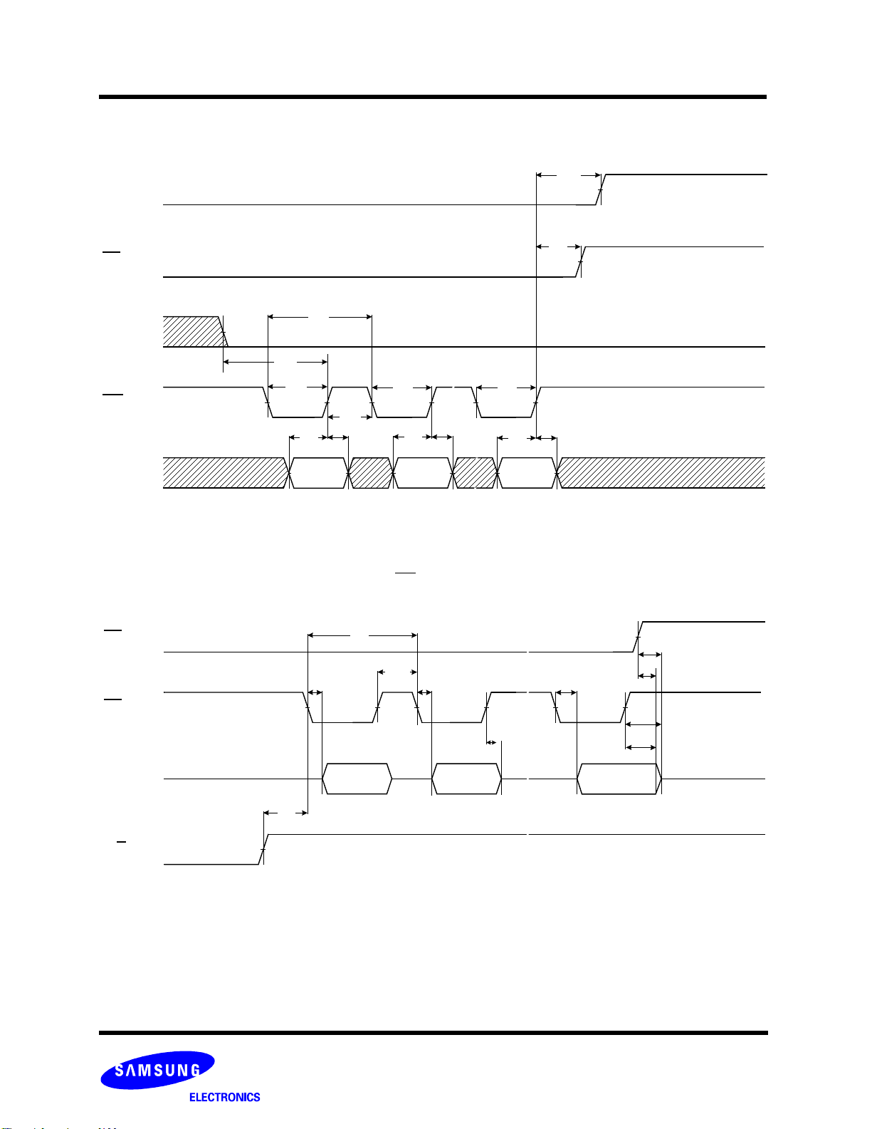
Erase Setup command(60h). Only address A
the block address loading initiates the internal erasing process. This two-step sequence of setup followed by execution command
ensures that memory contents are not accidentally erased due to external noise conditions.
At the rising edge of WE
the erase operation is completed, the Write Status Bit(I/O 0) may be checked. Figure 8 details the sequence.
after the erase confirm command input, the internal write controller handles erase and erase-verify. When
14 to A26 is valid while A9 to A13 is ignored. The Erase Confirm command(D0h) following
Figure 12. Block Erase Operation
tBERS
R/B
I/OX
60h
Address Input(3Cycle)
D0h
70h
I/O0
Pass
Block Add. : A14 ~ A25
Fail
30

K9F1208U0C
K9F1208R0C
BLOCK PROTECT
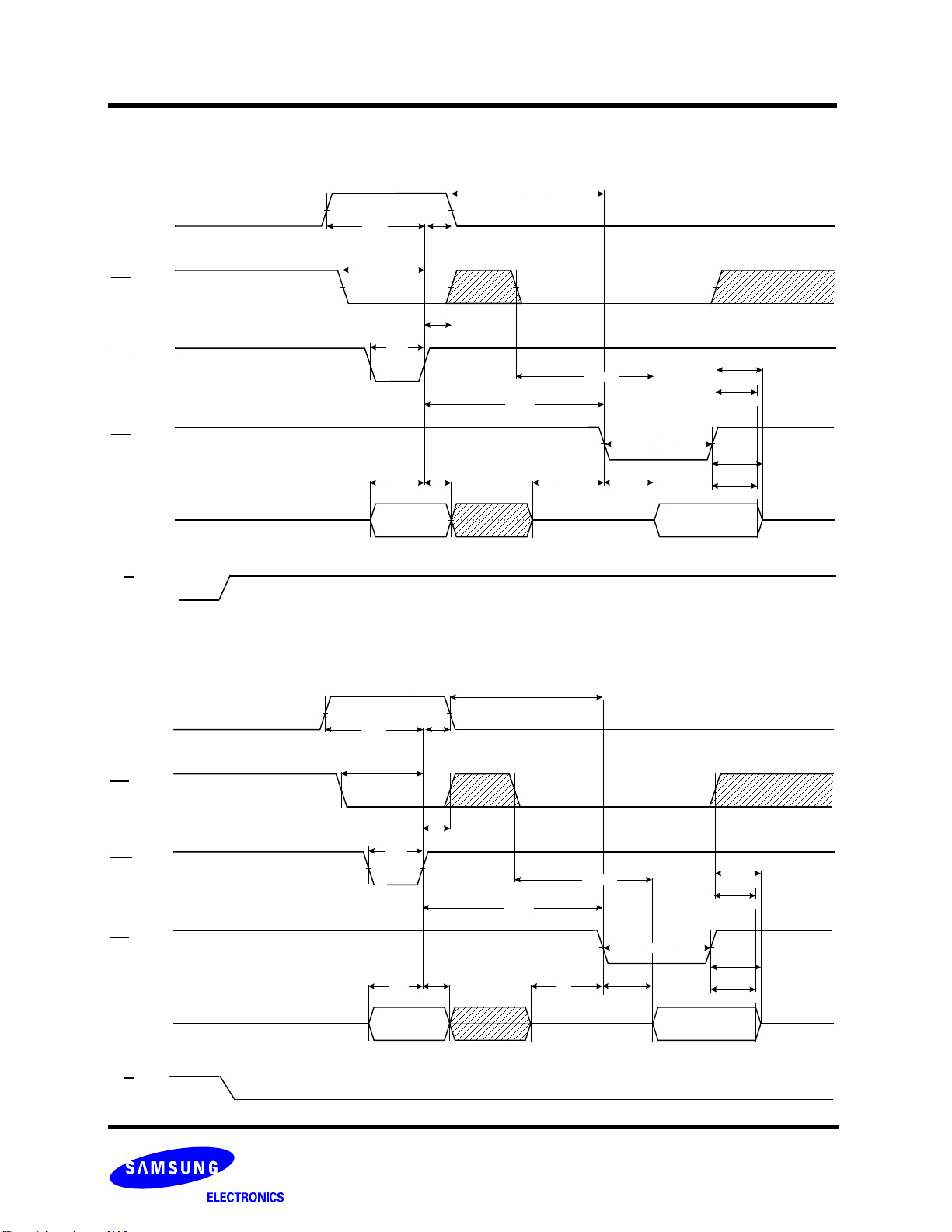
Each block is protected from programming and erasing, controlled by the protect flag written in a specified area in the block. Block
Proctect opreation is initiated by wirting 4xh-80h-10h to the command register along with four address cycles. Only address A
A
26 is valid while A0 to A13 is fixed as 00h. The data must not be loaded. Once the Block Protect opreation starts, the Read Status
Register command may be entered, with RE
of Page Program operation for protecting a block by monitoring the R/B
Read Status command and Reset command are valid while Block Protect operation is in progress. But, if Reset command is inputted
while Block Protect operation is in progress, the block will not be guaranteed whether it is protected or not. When the Page Program
operation for protecting a block is completed, the Write Status Bit(I/O 0) may be checked(Figure 13). The command register remains
in Read Status command mode until another valid command is written to the command register.
When programming is prohibited by 41h command, the protect flag and the data of protected block can be erased by Block Erase
operation. Once erasing is prohibited by 42h/43h command, the protect flag and the data of protected block can not be erased.
80h-10h is written to command register along with four address cycles at the program protected block or at the program/erase protected block, and if 60h-D0h is written to command register along with three address cycles at the program/erase protected block,
the R/B
pin changes to low for tR. The Block Protect operation must not be excuted on the aleady protected block. The Block Protect
operation will be aborted by Reset command(FFh). The Block Protect operation can only be used from first block to 200th block.
The device contains a Status Register which may be used to read out the state of the selected block. After writing 7Ah command to
the command register, a read cycle outputs the content of the Status Register to the I/O pins on the falling edge of CE
ever occurs last(Figure 14). Refer to table 3 for specific Status Register definitions. The command register remains in Status Read
mode until further commands are issued to it.
Three commands are provided to protect the block.
41h : Programming is prohibited
42h : Erasing is prohibited
43h : Both programming and erasing are prohibited
K9F1208B0C
FLASH MEMORY
14 to
and CE low, to read the status register. The system controller can detect the completion
output, or the Status bit(I/O 6) of the Status Register. Only the
or RE, which-
If
Figure 13. Block Protect Operation
R/B
I/OX
4Xh
80h
Address Input(4Cycle) I/O0
A0 ~ A7 : 00h Fix
A
9 ~ A13 : 00h Fix
14 ~ A25 : 0 to 4095
A
10h
tPROG
70h
Fail
Pass
FFh
FFh
31

K9F1208U0C
K9F1208R0C
Figure 14. Read Block Status
CLE
ALE
WE
K9F1208B0C
FLASH MEMORY
I/OX
00h A9 ~ A16A0 ~ A7 A25 7Ah Status
A0~7 : 00h, A9~13 : 0 fixed, A14~25 : 0 to 4095
A17 ~ A24
RE
tR
R/B
Table 3. Status Register Definition for 7Ah Command
I/O Status Definition
I/O 0 Programming Protect Not protected : "0" Protected : "1"
I/O 1 Erasing Protect Not protected : "0" Protected : "1"
I/O 2 Not use Don’t -cared
I/O 3 Not Use Don’t -cared
I/O 4 Not Use Don’t -cared
I/O 5 Not Use Don’t -cared
I/O 6 Device Operation Busy: "0" Ready : "1"
I/O 7 Write Protect Protected : "0" Not protect : "1"
NOTE :
1. I/Os defined ’Not use’ are recommended to be masked out when Read Status is being executed.
32
K9F1208U0C
K9F1208R0C
READ STATUS
The device contains a Status Register which may be read to find out whether program or erase operation is completed, and whether
the program or erase operation is completed successfully. After writing 70h command to the command register, a read cycle outputs
the content of the Status Register to the I/O pins on the falling edge of CE
the system to poll the progress of each device in multiple memory connections even when R/B
does not need to be toggled for updated status. Refer to table 4 for specific Status Register definitions. The command register
remains in Status Read mode until further commands are issued to it. Therefore, if the status register is read during a random read
cycle, a read command(00h or 50h) should be given before sequential page read cycle.
Table 4. Status Register Definition for 70h Command
I/O Page Program Block Erase Read Definition
I/O 0 Pass/Fail Pass/Fail Not use Pass : "0" Fail : "1"
I/O 1 Not use Not use Not use Don’t -cared
I/O 2 Not use Not use Not use Don’t -cared
I/O 3 Not Use Not Use Not Use Don’t -cared
I/O 4 Not Use Not Use Not Use Don’t -cared
I/O 5 Not Use Not Use Not Use Don’t -cared
I/O 6 Ready/Busy Ready/Busy Ready/Busy Busy : "0" Ready : "1"
I/O 7 Write Protect Write Protect Write Protect Protected : "0" Not Protected : "1"
NOTE : 1. I/Os defined ’Not use’ are recommended to be masked out when Read Status is being executed.
.
K9F1208B0C
FLASH MEMORY
or RE, whichever occurs last. This two line control allows
pins are common-wired. RE or CE
Read ID
The device contains a product identification mode, initiated by writing 90h to the command register, followed by an address input of
00h. Five read cycles sequentially output the manufacturer code(ECh), and the device code and 3rd, 4th cycle ID respectively. The
command register remains in Read ID mode until further commands are issued to it. Figure 15 shows the operation sequence.
Figure 15. Read ID Operation
CLE
tCEA
CE
WE
tAR
ALE
RE
I/O
0~7
90h
00h
Address. 1cycle
tWHR
tREA
ECh
Maker code
Device
Code
Device Device Code
K9F1208R0C 36h
5Ah
3Fh
33
K9F1208B0C 76h
K9F1208U0C 76h

K9F1208U0C
K9F1208R0C
RESET
The device offers a reset feature, executed by writing FFh to the command register. When the device is in Busy state during random
read, program or erase mode, the reset operation will abort these operations. The contents of memory cells being altered are no
longer valid, as the data will be partially programmed or erased. The command register is cleared to wait for the next command, and
the Status Register is cleared to value C0h when WP
accepted by the command register. The R/B
below.
Figure 16. RESET Operation
K9F1208B0C
FLASH MEMORY
is high. If the device is already in reset state a new reset command will be
pin changes to low for tRST after the Reset command is written. Refer to Figure 16
R/B
I/OX
FFh
tRST
Table 5. Device Status
After Power-up After Reset
Operation mode 00h Command is latched Waiting for next command
34
K9F1208U0C
K9F1208R0C
READY/BUSY
The device has a R/B output that provides a hardware method of indicating the completion of a page program, erase and random
read completion. The R/B
ter or random read is started after address loading. It returns to high when the internal controller has finished the operation. The pin is
an open-drain driver thereby allowing two or more R/B
current drain during busy(ibusy) , an appropriate value can be obtained with the following reference chart(Fig 17). Its value can be
determined by the following guidance.
VCC
GND
K9F1208B0C
pin is normally high but transitions to low after program or erase command is written to the command regis-
outputs to be Or-tied. Because pull-up resistor value is related to tr(R/B) and
Rp
R/B
open drain output
ibusy
Ready Vcc
1.8V device - VOL : 0.1V, VOH : Vcc-0.1V
2.7V device - VOL : 0.4V, VOH : VccQ-0.4V
3.3V device - V
OL : 0.4V, VOH : 2.4V
VOL : 0.4V, VOH : 2.4V
FLASH MEMORY
VOH
CL
VOL
Busy
tf
tr
Device
35

K9F1208U0C
K9F1208R0C
K9F1208B0C
@ Vcc = 1.8V, Ta = 25°C , C
= 30pF
L
FLASH MEMORY
300n 3m
tr,tf [s]
200n
100n
Ibusy
1.7
30
1.7
0.85
tr
60
1.7
tf
90
1.7
1K 2K 3K
0.57
120
0.43
1.7
4K
Rp(ohm)
@ Vcc = 2.7V, Ta = 25°C , C
300n 3m
tr,tf [s]
200n
100n
2.3
30
2.3
Ibusy
tr
tf
1.1
60
2.3
90
0.75
2.3
1K 2K 3K
= 30pF
L
120
0.55
2.3
4K
Rp(ohm)
@ Vcc = 3.3V, Ta = 25°C , C
= 100pF
L
2m
1m
2m
1m
Ibusy [A]
Ibusy [A]
2.4
300n 3m
tr,tf [s]
200n
Ibusy
1.2
200
300
0.8
tr
100n
100
3.6
3.6
tf
1K 2K 3K
Rp(ohm)
Figure 17. Rp vs tr ,tf & Rp vs ibusy
Rp value guidance
V
Rp(min, 1.8V part) =
Rp(min, 2.7V part) =
Rp(min, 3.3V part) =
where IL is the sum of the input currents of all devices tied to the R/B pin.
Rp(max) is determined by maximum permissible limit of tr
CC(Max.) - VOL(Max.)
IOL + ΣIL
V
CC(Max.) - VOL(Max.)
IOL + ΣIL
CC(Max.) - VOL(Max.)
V
IOL + ΣIL
=
=
=
3.6
1.85V
3mA
3mA
8mA
+ ΣIL
2.5V
+ ΣIL
3.2V
+ ΣIL
400
0.6
3.6
4K
2m
1m
Ibusy [A]
36

K9F1208U0C
K9F1208R0C
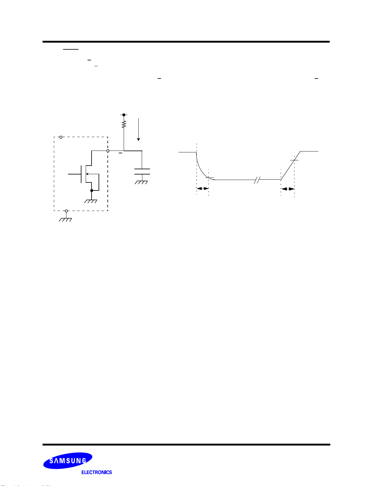
Data Protection & Power-up sequence
The device is designed to offer protection from any involuntary program/erase during power-transitions. An internal voltage detector
disables all functions whenever Vcc is below about 1.1V(1.8V device), 1.8V(2.7V device), 2V(3.3V device). WP
ware protection and is recommended to be kept at V
required before internal circuit gets ready for any command sequences as shown in Figure 18. The two step command sequence for
program/erase provides additional software protection.
Figure 18. AC Waveforms for Power Transition
K9F1208B0C
FLASH MEMORY
pin provides hard-
IL during power-up and power-down. A recovery time of minimum 100µs is
VCC
WP
WE
1.8V device : ~ 1.5V
2.7V device : ~ 2.0V
3.3V device : ~ 2.5V
100µs
High
1.8V device : ~ 1.5V
≈
2.7V device : ~ 2.0V
3.3V device : ~ 2.5V
≈
≈≈
37

K9F1208U0C
K9F1208R0C
WP AC Timing guide
Enabling WP during erase and program busy is prohibited. The erase and program operations are enabled and disabled as follows:
Figure A-1. Program Operation
1. Enable Mode
K9F1208B0C
WE
FLASH MEMORY
≈
I/O
WP
R/B
2. Disable Mode
WE
I/O
WP
R/B
Figure A-2. Erase Operation
1. Enable Mode
WE
80h 10h
tww(min.100ns)
≈
80h 10h
tww(min.100ns)
≈
R/B
2. Disable Mode
R/B
I/O
WP
WE
I/O
WP
60h D0h
tww(min.100ns)
≈
60h D0h
tww(min.100ns)
38
 Loading...