


现货库存、技术资料、百科信息、热点资讯,精彩尽在鼎好!
K5P2880YCM - T085
Document Title
Multi-Chip Package MEMORY
128M Bit (16Mx8) Nand Flash Memory / 8M Bit (1Mx8/512Kx16) Full CMOS SRAM
Revision History
Revision No.
0.0
History
Initial issue.
Draft Date
Jun. 11th 2001
Remark
Advanced
Information
Note : For more detailed features and specifications including FAQ, please refer to Samsung’s web site.
http://samsungelectronics.com/semiconductors/products/products_index.html
The attached datasheets are prepared and approved by SAMSUNG Electronics. SAMSUNG Electronics CO., LTD. reserve the right
to change the specifications. SAMSUNG Electronics will evaluate and reply to your requests and questions about device. If you have
any questions, please contact the SAMSUNG branch office near you.
- 1 -
Revision 0.0
June. 2001
K5P2880YCM - T085
Multi-Chip Package MEMORY
128M Bit (16Mx8) Nand Flash Memory / 8M Bit (1Mx8/512Kx16) Full CMOS SRAM
FEATURES
• Power Supply voltage : 2.7V to 3.3 V
• Organization
- Flash : (16M + 512K)bit x 8bit
- SRAM : 1M x 8 / 512K x 16 bit
• Access Time
- Flash : Random access : 10us(Max.), Serial read : 50ns(Min.)
- SRAM : 85 ns
• Power Consumption (typical value)
- Flash Read Current : 10 mA(@20MHz)
Program/Erase Current : 10 mA
Standby Current : 10 µA
- SRAM Operating Current : 20 mA
Standby Current : 0.5 µA
• Flash Automatic Program and Erase
Page Program : (512 + 16)Byte
Block Erase : (16K + 512)Byte
• Flash Fast Write Cycle Time
Program time : 300us(Typ.)
Block Erase Time : 2ms(Typ.)
• Flash Endurance : 100,000 Program/Erase Cycles Minimum
• Flash Data Retention : 10 years
• SRAM Data Retention : 1.5 V (min.)
• Operating Temperature : -25°C ~ 85°C
• Package : 69 - ball TBGA Type - 8 x 13mm, 0.8 mm pitch
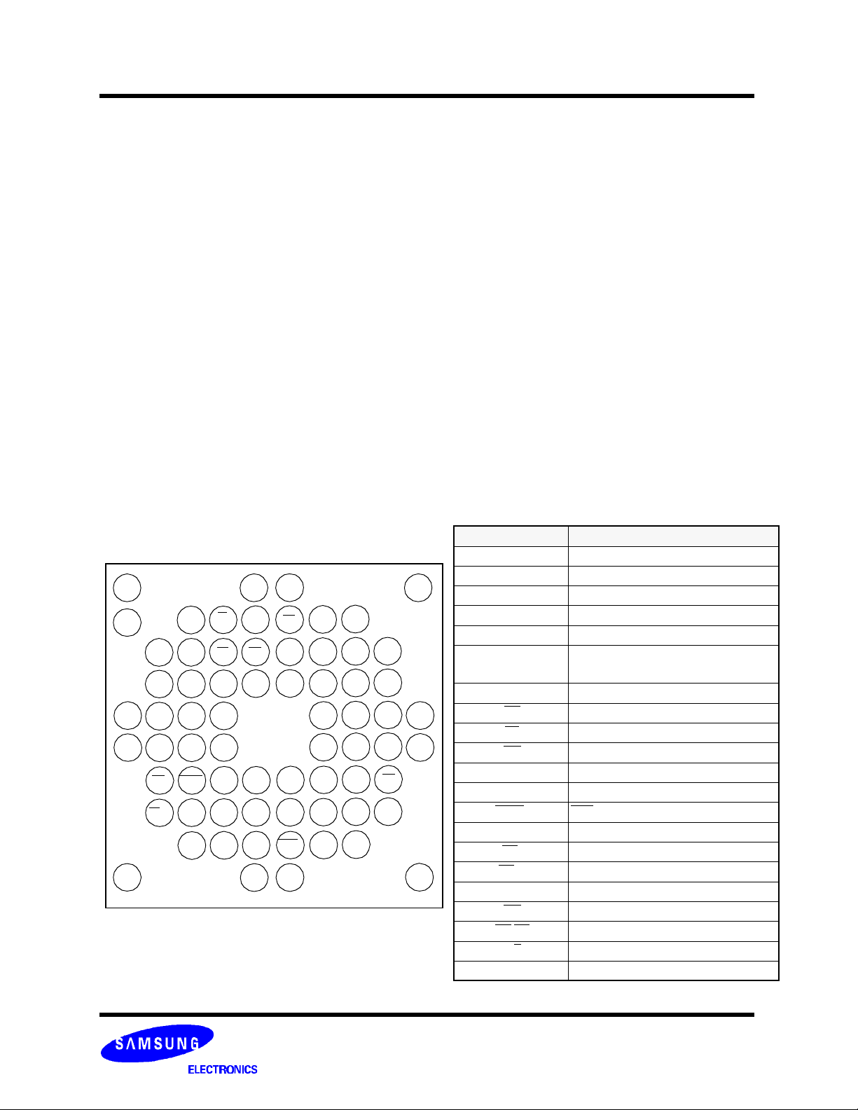
BALL CONFIGURATION
2
3
1
N.C
A
Index
B
N.C
N.C
A3A
A
2
A
1
A
0
OE/REDQ9DQ3
W
P
CS1
s
C
D
E
F
G
H
J
K
N.C
69 Ball TBGA , 0.8mm Pitch
SAMSUNG ELECTRONICS CO., LTD. reserves the right to change products and specifications without notice.
4
L
B
A
7
U
B
6
A5A18AL
A17
A
4
DQ1
V
S
S
DQ0DQ10Vc
DQ2DQ11
DQ8
Top View (Ball Down)
5
6
N.C
N.C
CLE
W
E
CS2sN.C
CEf
N.CA9
E
DQ4DQ13
c
QFVccSDQ1
BYT
E
S
N.C
N.C
7
A
A10
D
DQ5
GENERAL DESCRIPTION
The K5P2880YCM featuring single 3.0V power supply is a Multi
ChipPackage Memory which combines 128Mbit Nand Flash and
8Mbit full CMOS SRAM.
The 128Mbit Flash memory is organized as 16M x8 bit and the
8Mbit SRAM is organized as 1M x8 or 512K x16 bit. In 128Mb
NAND Flash a 528-byte page program can be typically achieved
within 300us and an 16K-byte block erase can be typically
achieved within 2ms. In serial read operation, a byte can be read
by 50ns. The I/O pins serve as the ports for address and data
input/output as well as command inputs. Even the write-intensive
systems can take advantage of the FLASH′s extended reliability
of 100K program/erase cycles by providing ECC(Error Correcting Code) with real time mapping-out algorithm. These algorithms
have been implemented in many mass storage applications and
also the spare 16 bytes of a page combined with the other 512
bytes can be utilized by system-level ECC. The 8Mbit SRAM supports the low data retention voltage for battery backup operation
with low current.
The K5P2880YCM is suitable for use in data memory of mobil
communication system to reduce not only mount area but also
power consumption. This device is available in 69-ball TBGA
Type.
BALL DESCRIPTION
8
A11
8
A12
A13
A14
S
A
6
Q
1
5
D
Q
DQ7
2
DQ1
4
A
N.C
Vcc
A16
R/B
Vss
1
0
9
N.C
1
5
f
N.C
N.C
N.C
Ball Name Description
A0 to A18 Address Input Balls (SRAM)
D/Q0 to D/Q7 Data Input/Output Balls (Common)
D/Q8 to D/Q15 Data Input/Output Balls (SRAM)
Vccs Power Supply (SRAM)
VccF Power Supply (Flash Memory)
VccQF
Output Buffer Power (Flash Memory)
This input may be tied directly to VCCF.
Vss Ground (Common)
UB Upper Byte Enable (SRAM)
LB Lower Byte Enable (SRAM)
WP Write Protection (Flash Memory)
CLE Command Latch Enable(Flash Memory)
ALE Address Latch Enable(Flash Memory)
BYTES Byte Control (SRAM)
SA Address Inputs (SRAM)
CEF Chip Enable (Flash Memory)
CS1S Chip Enable (SRAM Low Active)
CS2S Chip Enable (SRAM High Active)
WE Write Enable (Common)
OE/RE Output Enable (Common)
R/B Ready/Busy (Flash memory)
N.C No Connection
- 2 -
Revision 0.0
June. 2001
K5P2880YCM - T085
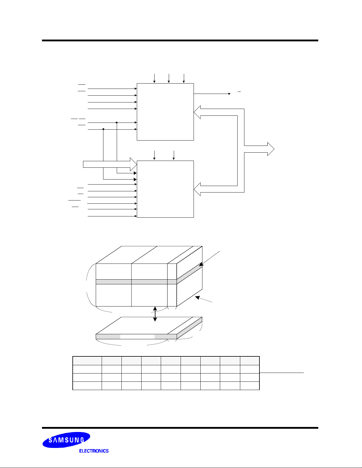
Figure 1. FUNCTIONAL BLOCK DIAGRAM
Vccf Vss VccQf
WP
CEf
CLE
ALE
OE/RE
WE
128 M bit
Flash Memory
R/B
DQ0 to DQ7
Vccs
Address(A0 to A18)
SA
UB
LB
BYTES
CS1S
CS2S
8 M bit
Static RAM
Figure 2. Flash ARRAY ORGANIZATION
32K Pages
(=1024 Blocks)
1st half Page Register
(=256 Bytes)
2nd half Page Register
(=256 Bytes)
512Bytes 16 Bytes
Vss
DQ0 to DQ15
DQ0 to DQ15
1 Block =32 Pages
= (16K + 512) Bytes
1 Page = 528 Bytes
1 Block = 528 Bytes x 32 Pages
= (16K + 512) Bytes
1 Device = 528 Bytes x 32Pages x 1024 Blocks
= 132 Mbits
8 bit
Page Register
512 Bytes
I/O 0 I/O 1 I/O 2 I/O 3 I/O 4 I/O 5 I/O 6 I/O 7
1st Cycle A0 A1 A2 A3 A4 A5 A6 A7
2nd Cycle A9 A10 A11 A12 A13 A14 A15 A16
3rd Cycle A17 A18 A19 A20 A21 A22 A23 *L
NOTE : Column Address : Starting Address of the Register.
00h Command(Read) : Defines the starting address of the 1st half of the register.
01h Command(Read) : Defines the starting address of the 2nd half of the register.
* A8 is set to "Low" or "High" by the 00h or 01h Command.
* L must be set to "Low"
16 Bytes
I/O 0 ~ I/O 7
- 3 -
Column Address
Row Address
(Page Address)
Revision 0.0
June. 2001
K5P2880YCM - T085
The NAND Flash is a 132Mbit(138,412,032 bit) memory organized as 32,768 rows(pages) by 528 columns. Spare 16 columns are
located in 512 to 527 column address. A 528-byte data register is connected to memory cell arrays accommodating data transfer
between the I/O buffers and memory during page read and page program operations. The memory array is made up of 16 cells that
ormed
d
operations are executed on a page basis, while erase operation is executed on a block basis. The memory array consists of 1024
n the NAND
s. This scheme dramatically reduces pin counts and allows systems
h
. Command Latch Enable(CLE) and Address
Latch Enable(ALE) are used to multiplex command and address respectively, via the I/O pins. All commands require one bus cycle
except Page Program command and Block Erase command which require two cycles: one cycle for setup and another for execution.
The 16M byte physical space requires 24 addresses, thereby requiring three cycles for byte-level addressing: column address, low
row address and high row address, in that order. Page Read and Page Program need the same three address cycles following
required command input. In Block Erase operation, however, only two row address cycles are used. Device operations are selected
NAND FLASH PRODUCT INTRODUCTION
are serially connected like NAND structure. Each of the 16 cells resides in a different page. A block consists of the 32 pages f
by one NAND structures, totaling 8448 NAND structures of 16 cells. The array organization is shown in Figure 2. Program and rea
blocks, and a block is separately erasable by 16K-byte unit. It indicates that the bit by bit erase operation is prohibited o
Flash.
The NAND Flash has addresses multiplexed with 8 I/O′
upgrades to future densities by maintaining consistency in system board design. Command, address and data are all written throug
I/O′s by bringing WE to low while CE is low. Data is latched on the rising edge of WE
by writing specific commands into command register. Table 1 defines the specific commands of the NAND Flash.
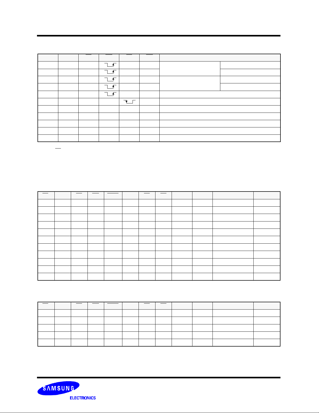
Table 1. COMMAND SETS
Function 1st. Cycle 2nd. Cycle Acceptable Command during Busy
Read 1
Read 2
Read ID 90h Reset FFh - O
Page Program 80h 10h
Block Erase 60h D0h
Read Status 70h - O
NOTE : 1. The 00h command defines starting address of the 1st half of registers.
The 01h command defines starting address of the 2nd half of registers.
After data access on the 2nd half of register by the 01h command, the status pointer is
automatically moved to the 1st half register(00h) on the next cycle.
00h/01h
50h
(1)
-
-
- 4 -
Revision 0.0
June. 2001
K5P2880YCM - T085
Table 2. FLASH MEMORY OPERATIONS TABLE
CLE ALE CE WE RE WP Mode
H L L H X
L H L H X Address Input(3clock)
H L L H H
L H L H H Address Input(3clock)
Read Mode
Write Mode
L L L H H Data Input
L L L H X Sequential Read & Data Output
L L X H H X During Read(Busy)
X X X X X H During Program(Busy)
X X X X X H During Erase(Busy)
X
X X H X X
NOTE : 1. X can be VIL or VIH.
2. WP should be biased to CMOS high or CMOS low for standby.
(1)
X
X X X L Write Protect
(2)
0V/VCC
Stand-by
Table 3. SRAM OPERATIONS TABLE
1. Word Mode
Command Input
Command Input
CS1 CS2 OE WE BYTE SA LB UB I/O0~7 I/O8~15 Mode Power
H X X X X X X X High-Z High-Z Deselected Standby
X L X X X X X X High-Z High-Z Deselected Standby
X X X X X X H H High-Z High-Z Deselected Standby
L H H H VCC X L X High-Z High-Z Output Disabled Active
L H H H VCC X X L High-Z High-Z Output Disabled Active
L H L H VCC X L H Dout High-Z Lower Byte Read Active
L H L H VCC X H L High-Z Dout Upper Byte Read Active
L H L H VCC X L L Dout Dout Word Read Active
L H X L VCC X L H Din High-Z Lower Byte Write Active
L H X L VCC X H L High-Z Din Upper Byte Write Active
L H X L VCC X L L Din Din Word Write Active
Note: X means don′t care. (Must be low or high state)
2. Byte Mode
CS1 CS2 OE WE BYTE SA LB UB I/O0~7 I/O8~15 Mode Power
H X X X X X X X High-Z High-Z Deselected Standby
X L X X X X X X High-Z High-Z Deselected Standby
L H H H VSS
L H L H VSS
L H X L VSS
Note: X means don′t care.(Must be low or high state)
1. Address input for byte operation.
SA
SA
SA
1)
DNU DNU High-Z DNU Output Disabled Active
1)
DNU DNU Dout DNU Lower Byte Read Active
1)
DNU DNU Din DNU Lower Byte Write Active
- 5 -
Revision 0.0
June. 2001
K5P2880YCM - T085
FLASH MEMORY OPERATION
PAGE READ
Upon initial device power up, the device status is initially Read1 command(00h) latched. This operation is also initiated by writing
00h to the command register along with three address cycles. Once the command is latched, it does not need to be written for the following page read operation. Two types of operation are available : random read, serial page read. The random read mode is enabled
when the page address is changed. The 528 bytes of data within the selected page are transferred to the data registers in less than
10µs(tR). The system controller can detect the completion of this data transfer(tR) by analyzing the output of R/B pin. Once the data
in a page is loaded into the registers, they may be read out by sequential RE pulse of 50ns period cycle. High to low transitions of the
RE clock take out the data from the selected column address up to the last column address.
Read1 and Read2 commands determine pointer which selects either main area or spare area. The spare area(512 to 527 bytes)
may be selectively accessed by writing the Read2 command. Addresses A0 to A3 set the starting address of spare area while
addresses A4 to A7 are ignored. To move the pointer back to the main area, Read1 command(00h/01h) is needed. Figures 3
through 4 show typical sequence and timing for each read operation.
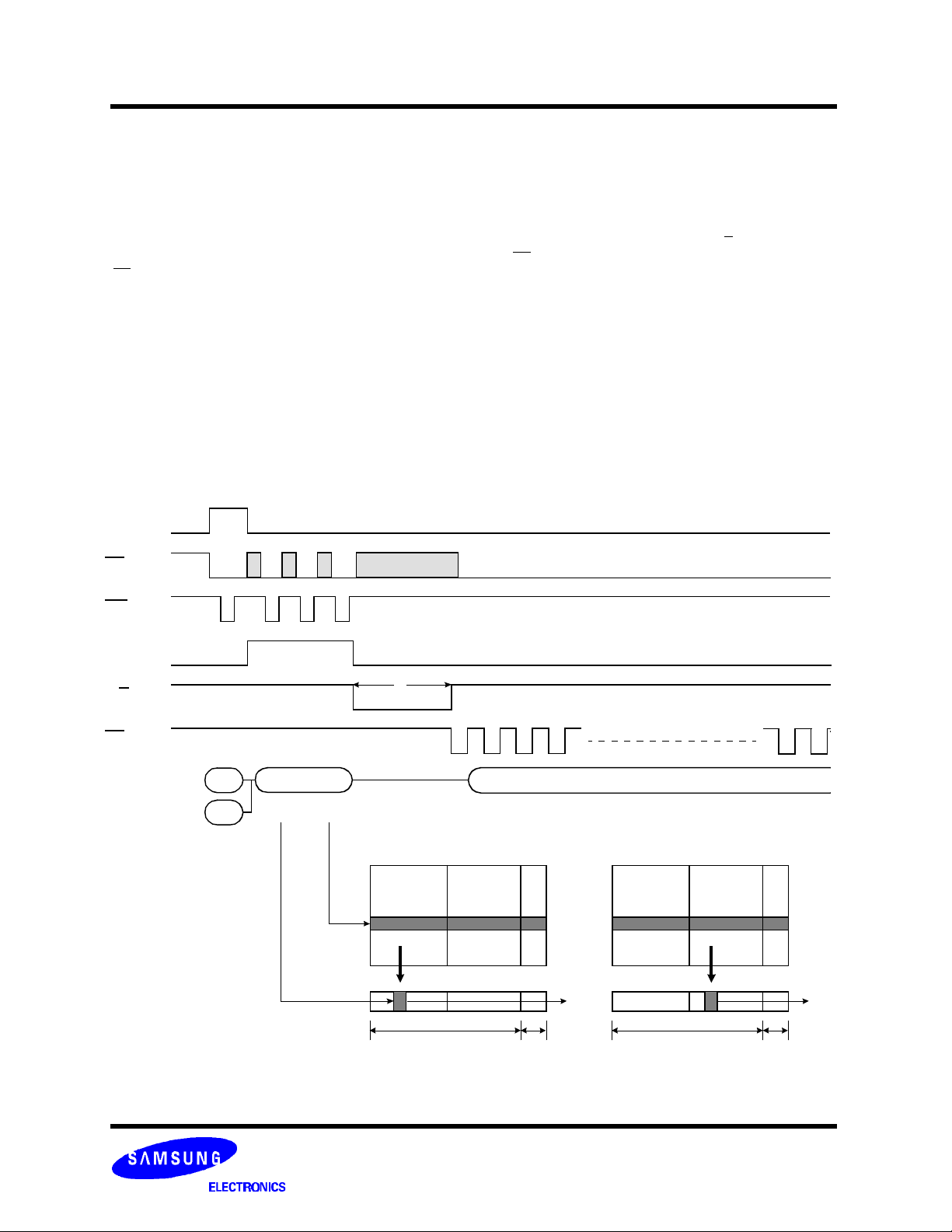
Figure 3,4 details the sequence.
Figure 3. Read1 Operation
CLE
CE
WE
ALE
R/B
RE
I/O0 ~ 7
01h
Start Add.(3Cycle)00h
A0 ~ A7 & A9 ~ A23
tR
(00h Command)
1st half array 2nd half array
Data Output(Sequential)
(01h Command)*
1st half array 2nd half array
Data Field Spare Field
* After data access on 2nd half array by 01H command, the start pointer is automatically moved to 1st half array (00h) at next cycle.
- 6 -
Data Field Spare Field
Revision 0.0
June. 2001
K5P2880YCM - T085
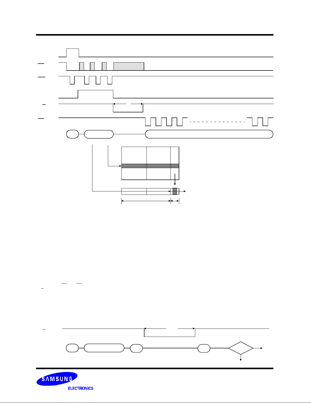
Figure 4. Read2 Operation
CLE
CE
WE
ALE
R/B
tR
RE
I/O0 ~ 7
50h
(A4 ~ A7 :
Don't Care)
Start Add.(3Cycle)
A0 ~ A3 & A9 ~ A23
1st half array 2nd half array
Data Field Spare Field
Data Output(Sequential)
Spare Field
PAGE PROGRAM
The device is programmed basically on a page basis, but it does allow multiple partial page programming of a byte or consecutive
bytes up to 528, in a single page program cycle. The number of consecutive partial page programming operation within the same
page without an intervening erase operation should not exceed 2 for main array and 3 for spare array. The addressing may be done
in any random order in a block. A page program cycle consists of a serial data loading period in which up to 528 bytes of data may be
loaded into the page register, followed by a non-volatile programming period where the loaded data is programmed into the appropriate cell. Serial data loading can be started from 2nd half array by moving pointer. About the pointer operation, please refer to the
attached technical notes.
The serial data loading period begins by inputting the Serial Data Input command(80h), followed by the three cycle address input and
then serial data loading. The bytes other than those to be programmed do not need to be loaded.The Page Program confirm command(10h) initiates the programming process. Writing 10h alone without previously entering the serial data will not initiate the programming process. The internal write state-control automatically executes the algorithms and timings necessary for program and
verify, thereby freeing the CPU for other tasks. Once the program process starts, the Read Status Register command may be
entered, with RE and CE low, to read the status register. The CPU can detect the completion of a program cycle by monitoring the
R/B output, or the Status bit(I/O 6) of the Status Register. Only the Read Status command and Reset command are valid while programming is in progress. When the Page Program is complete, the Write Status Bit(I/O 0) may be checked(Figure 5). The internal
write verify detects only errors for "1"s that are not successfully programmed to "0"s. The command register remains in Read Status
command mode until another valid command is written to the command register.
Figure 5. Program & Read Status Operation
R/B
I/O0 ~ 7
80h
Address & Data Input
A0 ~ A7 & A9 ~ A23
528 Byte Data
tPROG
10h 70h
- 7 -
I/O0
Fail
Revision 0.0
June. 2001
Pass
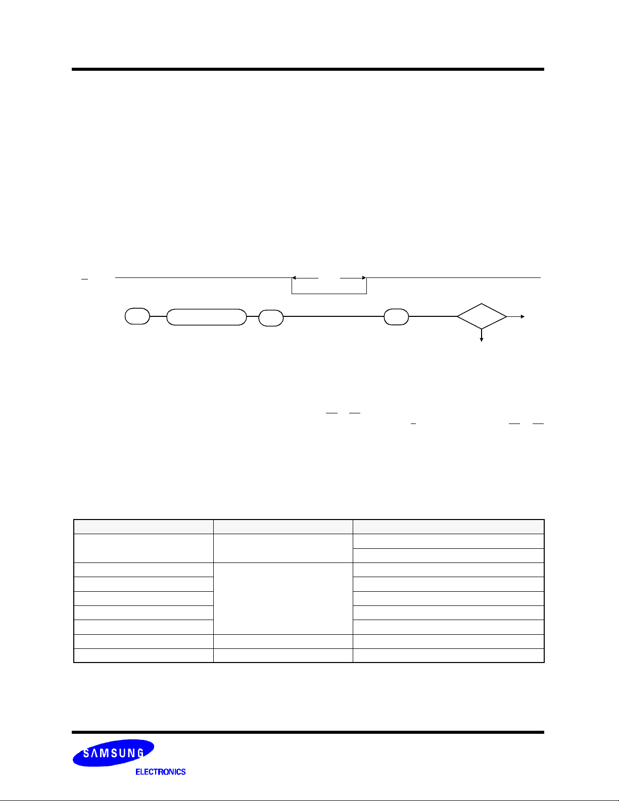
K5P2880YCM - T085
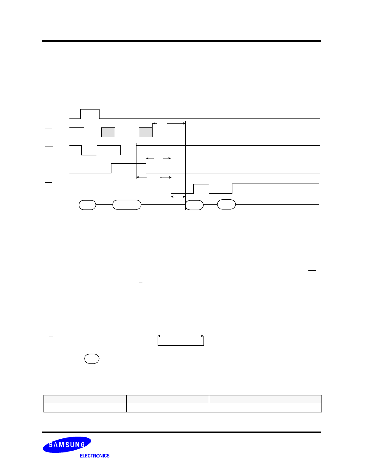
BLOCK ERASE
The Erase operation is done on a block(8K Byte) basis. Block address loading is accomplished in two cycles initiated by an Erase
Setup command(60h). Only address A14 to A23 is valid while A9 to A13 is ignored. The Erase Confirm command(D0h) following the
block address loading initiates the internal erasing process. This two-step sequence of setup followed by execution command
ensures that memory contents are not accidentally erased due to external noise conditions.
At the rising edge of WE after the erase confirm command input, the internal write state-control handles erase and erase-verify.
When the erase operation is completed, the Write Status Bit(I/O 0) may be checked.
Figure 6 details the sequence.
Figure 6. Block Erase Operation
R/B
I/O0 ~ 7
60h
Address Input(2Cycle)
Block Add. : A9 ~ A23
D0h
tBERS
70h
I/O0
Fail
Pass
READ STATUS
The device contains a Status Register which may be read to find out whether program or erase operation is completed, and whether
the program or erase operation is completed successfully. After writing 70h command to the command register, a read cycle outputs
the content of the Status Register to the I/O pins on the falling edge of CE or RE, whichever occurs last. This two line control allows
the system to poll the progress of each device in multiple memory connections even when R/B pins are common-wired. RE or CE
does not need to be toggled for updated status. Refer to table 4 for specific Status Register definitions. The command register
remains in Status Read mode until further commands are issued to it. Therefore, if the status register is read during a random read
cycle, a read command(00h or 50h) should be given before sequential page read cycle.
Table4. Read Status Register Definition
I/O # Status Definition
I/O0 Program / Erase
I/O1
I/O2 "0"
I/O3 "0"
I/O4 "0"
I/O5 "0"
I/O6 Device Operation "0" : Busy "1" : Ready
I/O7 Write Protect "0" : Protected "1" : Not Protected
Reserved for Future
Use
"0" : Successful Program / Erase
"1" : Error in Program / Erase
"0"
- 8 -
Revision 0.0
June. 2001
K5P2880YCM - T085
READ ID
The device contains a product identification mode, initiated by writing 90h to the command register, followed by an address input of
00h. Two read cycles sequentially output the manufacture code(ECh), and the device code (73h) respectively. The command register remains in Read ID mode until further commands are issued to it. Figure 7 shows the operation sequence.
Figure 7. Read ID Operation
CLE
tCEA
CE
WE
tAR1
ALE
tWHR
RE
I/O0~7
90h
00h
Address. 1cycle
tREA
ECh
Maker code
73h
Device code
RESET
The device offers a reset feature, executed by writing FFh to the command register. When the device is in Busy state during random
read, program or erase modes, the reset operation will abort these operation. The contents of memory cells being altered are no
longer valid, as the data will be partially programmed or erased. Internal address registers are cleared to "0"s and data registers to
"1"s. The command register is cleared to wait for the next command, and the Status Register is cleared to value C0h when WP is
high. Refer to table 5 for device status after reset operation. If the device is already in reset state a new reset command will not be
accepted to by the command register. The R/B pin transitions to low for tRST after the Reset command is written. Reset command is
not necessary for normal operation. Refer to Figure 8 below.
Figure 8. RESET Operation
tRST
R/B
FFhI/O0 ~ 7
Table5. Device Status
Operation Mode Read 1 Waiting for next command
After Power-up After Reset
- 9 -
Revision 0.0
June. 2001

K5P2880YCM - T085
READY/BUSY
The device has a R/B output that provides a hardware method of indicating the completion of a page program, erase and random
read completion. The R/B pin is normally high but transitions to low after program or erase command is written to the command register or random read is started after address loading. It returns to high when the internal controller has finished the operation. The pin
is an open-drain driver thereby allowing two or more R/B outputs to be Or-tied. An appropriate pull-up resister is required for proper
operation and the value may be calculated by the following equation.
VCC
GND
Device
Rp
R/B
open drain output
VCC(Max.) - VOL(Max.)
Rp =
where IL is the sum of the input currents of all devices tied to the
R/B pin.
IOL + ∑IL
=
2.9V
8mA + ∑IL
DATA PROTECTION
The device is designed to offer protection from any involuntary program/erase during power-transitions. An internal voltage detector
disables all functions whenever Vcc is below about 2V. WP pin provides hardware protection and is recommended to be kept at VIL
during power-up and power-down as shown in Figure 9. The two step command sequence for program/erase provides additional
software protection.
Figure 9. AC Waveforms for Power Transition
VCC
WP
~ 2.2V
High
- 10 -
≈≈
~ 2.2V
Revision 0.0
June. 2001

K5P2880YCM - T085
NAND Flash Technical Notes
Invalid Block(s)
Invalid blocks are defined as blocks that contain one or more invalid bits whose reliability is not guaranteed by Samsung. The information regarding the invalid block(s) is so called as the invalid block information. Devices with invalid block(s) have the same quality
level or as devices with all valid blocks and have the same AC and DC characteristics. An invalid block(s) does not affect the performance of valid block(s) because it is isolated from the bit line and the common source line by a select transistor. The system design
must be able to mask out the invalid block(s) via address mapping. The 1st block of the NAND Flash, however, is fully guaranteed to
be a valid block.
Identifying Invalid Block(s)
All device locations are erased(FFh) except locations where the invalid block(s) information is written prior to shipping. The invalid
block(s) status is defined by the 6th byte in the spare area. Samsung makes sure that either the 1st or 2nd page of every invalid
block has non-FFh data at the column address of 517. Since the invalid block information is also erasable in most cases, it is impossible to recover the information once it has been erased. Therefore, the system must be able to recognize the invalid block(s) based
on the original invalid block information and create the invalid block table via the following suggested flow chart(Figure 10). Any
intentional erasure of the original invalid block information is prohibited.
Increment Block Address
Create (or update)
Invalid Block(s) Table
Start
Set Block Address = 0
No
No
Check "FFh" ?
Yes
Last Block ?
Yes
End
Check "FFh" at the column address 517
*
of the 1st and 2nd page in the block
Figure 10. Flow chart to create invalid block table
- 11 -
Revision 0.0
June. 2001

K5P2880YCM - T085
Error in write or read operation
Over its life time, the additional invalid blocks may develop with NAND Flash memory. Refer to the qualification report for the actual
data.The following possible failure modes should be considered to implement a highly reliable system. In the case of status read failure after erase or program, block replacement should be done. To improve the efficiency of memory space, it is recommended that
the read or verification failure due to single bit error be reclaimed by ECC without any block replacement. The said additional block
failure rate does not include those reclaimed blocks.
Failure Mode Detection and Countermeasure sequence
Erase Failure Status Read after Erase --> Block Replacement
Write
Read Single Bit Failure Verify ECC -> ECC Correction
Program Failure
Status Read after Program --> Block Replacement
Read back ( Verify after Program) --> Block Replacement
or ECC Correction
ECC
: Error Correcting Code --> Hamming Code etc.
Example) 1bit correction & 2bit detection
Figure 11. Flash Program flow chart
Start
Write 80h
Write Address
Write Data
Write 10h
Read Status Registe
I/O 6 = 1 ?
or R/B = 1 ?
Yes
*
Program Error
No
I/O 0 = 0 ?
No
If ECC is used, this verification
: If program operation results in an error, map out
*
the block including the page in error and copy the
target data to another block.
operation is not needed.
Write 00h
Write Address
Wait for tR Time
Verify Data
Yes
Program Completed
No
Program Error
*
Yes
- 12 -
Revision 0.0
June. 2001

K5P2880YCM - T085
Figure 12. Flash Erase Flow Chart
Start
Write 60h
Write Block Address
Write D0h
Read Status Register
I/O 6 = 1 ?
or R/B = 1 ?
Yes
*
Erase Error
No
I/O 0 = 0 ?
Yes
No
Figure 13. Flash Read Flow Chart
Start
Write 00h
Write Address
Read Data
ECC Generation
Reclaim the Error
No
Verify ECC
Yes
Page Read Completed
Erase Completed
: If erase operation results in an error, map out
*
the failing block and replace it with another block.
Figure 14. Flash Block Replacement
Buffer
memory
error occurs
Page a
Block A
Block B
When the error happens with page "a" of Block "A", try
to write the data into another Block "B" from an external buffer. Then, prevent further system access to
Block "A" (by creating a "invalid block" table or other
appropriate scheme.)
- 13 -
Revision 0.0
June. 2001

K5P2880YCM - T085
Pointer Operation of NAND Flash
The Flash memory has three modes to set the destination of the pointer. The pointer is set to "A" area by the "00h" command, to "B"
area by the "01h" command, and to "C" area by the "50h" command. Table 6 shows the destination of the pointer, and figure 15
shows the block diagram of its operations.
Table 6. Destination of the pointer
Command Pointer position Area
00h
01h
50h
0 ~ 255 byte
256 ~ 511 byte
512 ~ 527 byte
1st half array(A)
2nd half array(B)
spare array(C)
Example of Programming with successive Pointer Operation
(1) "A" area program
50h
(2) "B" area program
00h
"C" area
"A" area
00h 80h
"A" area
01h 80h
"B" area
Address / Data input
Address / Data input
"A" area
(00h plane)
256 Byte
"A" "B" "C"
Pointer select
commnad
(00h, 01h, 50h)
"B" area
(01h plane)
256 Byte 16 Byte
Pointer
"C" area
(50h plane)
Internal
Page Register
Figure 15. Block Diagram of Pointer Operation
Address / Data input
10h 80h 10h
"A" area program
Address / Data input
10h 80h 10h
"B" area program
"A" area program
"A" area program
(3) "C" area program
00h
"A" area
50h 80h
"C" area
Address / Data input
10h 80h 10h
"C" area program
Table 7. Pointer Status after each operation
Operation Pointer status after operation
Program
Reset
Power up
* 01h command is valid just one time when it is used as a pointer for program/erase.
* Erase operation does not affect the pointer status. Previous pointer status is maintained.
With previous 00h, Device is set to 00h Plane
With previous 01h, Device is set to 00h Plane*
With previous 50h, Device is set to 50h Plane
"00h" Plane("A" area)
"00h" Plane("A" area)
- 14 -
Address / Data input
"C" area program
Revision 0.0
June. 2001

K5P2880YCM - T085
System Interface Using CE don’t-care.
For an easier system interface, CE may be inactive during data-loading or sequential data-reading as shown below. The internal
528byte page registers are utilized as seperate buffers for this operation and the system design gets more flexible. In addition, for
voice or audio applications which use slow cycle time on the order of u-seconds, de-activating CE during the data-loading and reading would provide significant saving in power consumption.
Figure 16. Program Operation with CE don’t-care.
CLE
CE don’t-care
CE
WE
ALE
I/O0~7
(Min. 10ns)
tCS
CE
WE
Figure 17. Read Operation with CE don’t-care.
CLE
CE
Start Add.(3Cycle)80h Data Input
tCH
tWP
≈
CE
RE
I/O0~7
(Max. 45ns)
tCEA
tREA
CE don’t-care
≈
Data Input
out
10h
RE
ALE
R/B
WE
I/O0~7
≈
tR
Start Add.(3Cycle)00h
- 15 -
Data Output(sequential)
Revision 0.0
June. 2001

K5P2880YCM - T085
ABSOLUTE MAXIMUM RATINGS
Parameter Symbol Rating Unit
VIN -0.5 to (Vccf,Vccs)+ 0.3 V
Voltage on any pin relative to VSS
Temperature Under Bias TBIAS -25 to + 125
Storage Temperature TSTG -65 to + 150 °C
NOTE :
1. Minimum DC voltage is -0.5V on input/output pins. During transitions, this level may undershoot to -2.0V for periods <30ns.
Maximum DC voltage on input/output pins is VCCQ+0.3V which, during transitions, may overshoot to VCC+2.0V for periods <20ns.
2. Permanent device damage may occur if ABSOLUTE MAXIMUM RATINGS are exceeded. Functional operation should be restricted to the conditions
as detailed in the operational sections of this data sheet. Exposure to absolute maximum rating conditions for extended periods may affect reliability.
RECOMMENDED OPERATING CONDITIONS
(Voltage reference to GND, TA=-25 to 85°C)
Parameter Symbol Min Typ. Max Unit
Supply Voltage VCCf, VCCs 2.7 3.0 3.3 V
Supply Voltage VCCQ 2.7 3.0 3.3 V
Supply Voltage VSS 0 0 0 V
VCCf, VCCs -0.2 to 3.6V V
VccQ -0.2 to 3.6V
°C
DC AND OPERATING CHARACTERISTICS(Recommended operating conditions otherwise noted.)
Parameter Symbol Test Conditions Min Max Unit
Input Leakage Current ILI
Output Leakage Current ILO
Input Low Voltage Level, All inputs VIL -0.4 0.4
Input High Voltage Level VIH VccQf-0.4 VccQf+0.4
Output Low Voltage Level
Output High Voltage Level VOH
VCCf,VCCS=VCCfMax.,VCCSMax.
VCCQf=VCCQfMax.,VIN=VCCQf or GND
VCCf,VCCS=VCCfMax.,VCCSMax.
VCCQf=VCCQfMax.,VIN=VCCQf or GND
Vccf/=Vccf Min, Vccs=Vccs Min
VOL
IOL = 0.1mA
Vccf=Vccf Min, Vccs=Vccs Min.
IOH = -0.1mA
- ±10 µA
- ±10 µA
- 0.4
VccQ-0.3 -
V
- 16 -
Revision 0.0
June. 2001

K5P2880YCM - T085
DC AND OPERATING CHARACTERISTICS(Continued)
Test Conditions
Flash
SRAM
Parameter Symbol
Active Sequential Read
Currnt
Active Program Current ICC2f VCCf=VCCfMax,VCCQf=VCCQfMax 10 20 mA
Active Erase Current ICC3f VCCf=VCCfMax,VCCQf=VCCQfMax 10 20 mA
Stand_by Current ISB2f CEf=VccQf, WP=0V/VCCQf 10 50 µA
Operating Current
Stand_by Current(CMOS) ISB2s
ICC1f
ICC1s
ICC2s
tRC=50ns,CEf=VIL, IOUT=0mA
VCCf=VCCfMax,VCCQf=VCCQfMax
Cycle time=1µs, 100% duty, CS1s≤0.2V,
CS2s≥VccS-0.2V, All outputs open
VIN≤0.2V or VIN≥VCCS-0.2V
Cycle time=Min, 100% duty, CS1s=VIL,
CS2s=VIH
All outputs open, VIN=VIL or VIH
CS1s≥VccS-0.2V, CS2s≥VccS-0.2V (CS1s
controlled) or CS2s≤0.2V (CS2s controlled),
BYTES=VSS or VCCS
Other input =0~VccS
Typ
10 20 mA
Max
5 mA
30 mA
15 µA
Unit
CAPACITANCE (TA = 25 °C, VCC = 3.0V, f = 1.0MHz)
Item Symbol Test Condition Min Max Unit
Input/Output Capacitance CI/O VIL=0V - 20 pF
Input Capacitance CIN VIN=0V - 18 pF
Note : Capacitance is periodically sampled and not 100% tested.
VALID BLOCK OF FLASH MEMORY
Parameter Symbol Min Typ. Max Unit
Valid Block Number NVB 1014 1020 1024 Blocks
NOTE :
1. The Flash memory may include invalid blocks when first shipped. Additional invalid blocks may develop while being used. The number of valid
blocks is presented with both cases of invalid blocks considered. Invalid blocks are defined as blocks that contain one or more bad bits. Do not try to
access these invalid blocks for program and erase. Refer to the attached technical notes for a appropriate management of invalid blocks.
2. The 1st block, which is placed on 00h block address, is guaranteed to be a valid block.
- 17 -
Revision 0.0
June. 2001

K5P2880YCM - T085
AC TEST CONDITION
Parameter Value
Input Pulse Levels 0V to VccQf
Input Rise and Fall Times 5ns
Input and Output Timing Levels VccQf/2
Output Load
Note : AC test inputs are driven at VccQ for a logic "1" and 0.0V for a logic "0". Input timing begins, and output timing ends, at VccQ / 2.
Input rise and fall times (10% - 90%)<5ns. Worst case speed condition are when VccQf = VccQf Min.
1TTL gate and CL = 50pF
VccQf
0V
VccQf
2
Device
Under Test
Input & Output
Test Point
Input Pulse and Test Point
VccQ
CL
VccQf
2
25K
Out
25K
- 18 -
Revision 0.0
June. 2001

K5P2880YCM - T085
Flash Program/Erase Characteristics
Parameter Symbol Min Typ Max Unit
Program Time tPROG - 300 600 µs
Number of Partial Program Cycles
in the Same Page
Block Erase Time tBERS - 2 4 ms
Main Array
Spare Array - - 3 cycles
Nop
Flash AC Timing Characteristics for Command / Address / Data Input
Parameter Symbol Min Max Unit
CLE Set-up Time tCLS 0 - ns
CLE Hold Time tCLH 10 - ns
CE Setup Time tCS 0 - ns
CE Hold Time tCH 10 - ns
WE Pulse Width tWP 25 - ns
ALE Setup Time tALS 0 - ns
ALE Hold Time tALH 10 - ns
Data Setup Time tDS 20 - ns
Data Hold Time tDH 10 - ns
Write Cycle Time tWC 50 - ns
WE High Hold Time
tWH 15 - ns
- - 2 cycles
Flash AC Characteristics for Operation
Parameter Symbol Min Max Unit
Data Transfer from Cell to Register tR - 10
ALE to RE Delay( ID read ) tAR1 20 - ns
ALE to RE Delay(Read cycle) tAR2 50 - ns
CE Access Time tCEA - 45 ns
Ready to RE Low tRR 20 - ns
RE Pulse Width tRP 30 - ns
WE High to Busy tWB - 100 ns
Read Cycle Time tRC 50 - ns
RE Access Time tREA - 35 ns
RE High to Output Hi-Z tRHZ 15 30 ns
CE High to Output Hi-Z
RE High Hold Time tREH 15 - ns
Output Hi-Z to RE Low tIR 0 - ns
WE High to RE Low tWHR 60 - ns
Device Resetting Time(Read/Program/Erase) tRST - 5/10/500
NOTE :
1. If reset command(FFh) is written at Ready state, the device goes into Busy for maximum 5us
tCHZ - 20 ns
(1)
µs
µs
- 19 -
Revision 0.0
June. 2001

K5P2880YCM - T085
* Command Latch Cycle
CLE
CE
WE
ALE
I/O0~7
* Address Latch Cycle
tCLS
tCS
tALS
tWP
tDS
Command
tCLH
tCH
tALH
tDH
CLE
CE
WE
ALE
I/O0~7
tCLS
tCS tWC
tWP
tALS
tALH tALS
tDS
A0~A7
tDH
tWH
- 20 -
tWP
tDS
A9~A16
tWC
tWH
tALH tALS
tDH
tWP
tDS
A17~A23
tALH
tDH
Revision 0.0
June. 2001

K5P2880YCM - T085
* Input Data Latch Cycle
CLE
CE
tCLH
tCH
tWP
tWC
tDS
DIN 0
tDH
tWH
tWP
tDS
DIN 1
≈
tDH
tALS
ALE
WE
I/O0~7
* Sequential Out Cycle after Read(CLE=L, WE=H, ALE=L)
tREA
tRC
tREH
tREA
CE
≈≈
tWP
tDS
DIN 511
tDH
≈≈≈≈
tREA
tCHZ*
RE
I/O0~7
R/B
tRHZ*
Dout
tRR
NOTES : Transition is measured ±200mV from steady state voltage with load.
This parameter is sampled and not 100% tested.
Dout
- 21 -
tRHZ*
Dout
Revision 0.0
June. 2001

K5P2880YCM - T085
* Status Read Cycle
CLE
CE
WE
RE
tCLS
tCS
tCLS
tCLH
tCH
tWP
tWHR
tDH tREA
tDS
tIR
tCEA
tCHZ
tRHZ
I/O0~7
READ1 OPERATION(READ ONE PAGE)
CLE
CE
tWC
WE
ALE
RE
Column
Address
A9 ~ A16 A17 ~ A23
Page(Row)
Address
I/O0~7
R/B
00h or 01h A0 ~ A7
70h
tWB
tR
tRR
Busy
tAR2
Dout N
tRC
Dout N+1 Dout N+2
Status Output
Dout N+3
tCHZ
tRHZ
≈
≈
Dout 527
≈
- 22 -
Revision 0.0
June. 2001

K5P2880YCM - T085
READ2 OPERATION(READ ONE PAGE)
CLE
CE
WE
ALE
RE
I/O0 ~ 7
50h
A0 ~ A7
R/B
M Address
PAGE PROGRAM OPERATION
CLE
tWB
A9 ~ A16 A17 ~ A23
A0 ~ A3 :Valid Address
A4 ~ A7 :Dont care
tR
tAR2
tRR
≈≈
≈
Dout
511+M
Selected
Row
Dout
511+M+1
Dout 527
512 16
address M
Start
CE
WE
ALE
RE
I/O0 ~ 7
R/B
tWC
80h 70h I/O0
Sequential Data
Input Command
A0 ~ A7 A17 ~ A23A9 ~ A16
Column
Address
tWC
Page(Row)
Address
DinNDin
1 up to 528 Byte Data
Sequential Input
N+1
- 23 -
tWC
tWB
tPROG
≈≈
Din
527
10h
Program
Command
Read Status
Command
≈
I/O0=0 Successful Program
I/O0=1 Error in Program
Revision 0.0
June. 2001

K5P2880YCM - T085
BLOCK ERASE OPERATION(ERASE ONE BLOCK)
CLE
CE
tWC
WE
tWB
ALE
RE
tBERS
I/O0~7
60h
A17 ~ A23A9 ~ A16
Page(Row)
Address
DOh 70h I/O 0
R/B
Auto Block Erase
Setup Command
Erase Command Read Status
MANUFACTURE & DEVICE ID READ OPERATION
CLE
CE
WE
ALE
Busy
≈
Command
I/O0=0 Successful Erase
I/O0=1 Error in Erase
RE
I/O0 ~ 7
tREA
90h
Read ID Command Maker Code Device Code
00h ECh 73h
Address 1st Cycle
- 24 -
Revision 0.0
June. 2001

K5P2880YCM - T085
SRAM AC CHARACTERISTICS
Read
Write
Parameter List Symbol
Read cycle time tRC 85 - ns
Address access time tAA - 85 ns
Chip select to output tCO1, tCO2 - 85 ns
Output enable to valid output tOE - 45 ns
UB, LB Access Time tBA - 85 ns
Chip select to low-Z output tLZ1, tLZ2 10 - ns
UB, LB enable to low-Z output tBLZ 10 - ns
Output enable to low-Z output tOLZ 5 - ns
Chip disable to high-Z output tHZ1, tHZ2 0 25 ns
UB, LB disable to high-Z output tBHZ 0 25 ns
Output disable to high-Z output tOHZ 0 25 ns
Output hold from address change tOH 15 - ns
Write cycle time tWC 85 - ns
Chip select to end of write tCW 70 - ns
Address set-up time tAS 0 - ns
Address valid to end of write tAW 70 - ns
UB, LB Valid to End of Write tBW 70 - ns
Write pulse width tWP 60 - ns
Write recovery time tWR 0 - ns
Write to output high-Z tWHZ 0 25 ns
Data to write time overlap tDW 35 - ns
Data hold from write time tDH 0 - ns
End write to output low-Z tOW 5 - ns
85ns
Min Max
Units
SRAM DATA RETENTION CHARACTERISTICS
Item Symbol Test Condition Min Typ Max Unit
Vccs for data retention VDR CS1s≥Vccs-0.2V 1) 1.5 - 3.3 V
Data retention current IDR Vccs=3.0V, CS1s≥Vccs-0.2V 1)
Data retention set-up time tSDR
Recovery time tRDR tRC - -
1. CS1s≥Vccs-0.2V, CS2s≥Vccs-0.2V(CS1s controlled) or CS2s≤0.2V(CS2s controlled), BYTE=Vss or Vcc.
2. Typical values are not 100% tested
See data retention waveform
- 25 -
25 °C
85 °C - 25
2.0 2) 5
-
0 - -
Revision 0.0
June. 2001
µA
ns

K5P2880YCM - T085
SRAM TIMMING DIAGRAMS
TIMING WAVEFORM OF READ CYCLE(1) (Address Controlled, CS1S=OE=VIL, CS2S=WE=VIH, UB or/and LB=VIL)
tRC
Address
tAA
tCO1
tAA
Data Valid
tRC
tOH
tOH
Data Out
Previous Data Valid
TIMING WAVEFORM OF READ CYCLE(2) (WE=VIH , if CIOs is low, ignore UB/LB timing)
Address
CS1S
CS2S
UB, LB
OE
Data out
NOTES (READ CYCLE)
1. tHZ and tOHZ are defined as the time at which the outputs achieve the open circuit conditions and are not referenced to output voltage
levels.
2. At any given temperature and voltage condition, tHZ(Max.) is less than tLZ(Min.) both for a given device and from device to device
interconnection.
High-Z
tLZ
tOLZ
tBLZ
tCO2
tHZ
tBA
tBHZ
tOE
tOHZ
Data Valid
- 26 -
Revision 0.0
June. 2001

K5P2880YCM - T085
SRAM TIMMING DIAGRAMS
TIMING WAVEFORM OF WRITE CYCLE(1) (WE Controlled, if CIOs is low, ignore UB/LB timing)
tWC
Address
CS1S
CS2S
UB, LB
WE
Data in
Data out
tCW(2)
tAW
tCW(2)
tBW
tWP(1)
tAS(3)
tDW
High-Z
tWHZ
Data Undefined
tWR(4)
tDH
Data Valid
tOW
TIMING WAVEFORM OF WRITE CYCLE(2) (CS1S Controlled, if CIOs is low, ignore UB/LB timing)
tWC
Address
tAS(3)
CS1S
tCW(2)
tAW
tWR(4)
High-Z
CS2S
UB, LB
WE
Data in
Data out
tBW
tWP(1)
tDW
Data Valid
High-Z High-Z
- 27 -
tDH
Revision 0.0
June. 2001

K5P2880YCM - T085
TIMING WAVEFORM OF WRITE CYCLE(3) (UB, LB Controlled, CIOs must be high.)
tWC
Address
tCW(2)
CS1S
tAW
tWR(4)
CS2S
UB, LB
WE
Data in
Data out
NOTES (WRITE CYCLE)
1. A write occurs during the overlap(tWP) of low CS1S and low WE. A write begins when CS1S goes low and WE goes low with asserting
UB or LB for single byte operation or simultaneously asserting UB and LB for double byte operation. A write ends at the earliest tran-
sition when CS1S goes high and WE goes high. The tWP is measured from the beginning of write to the end of write.
2. tCW is measured from the CS1S going low to end of write.
3. tAS is measured from the address valid to the beginning of write.
4. tWR is measured from the end or write to the address change. tWR applied in case a write ends as CS1S or WE going high.
tAS(3)
High-Z
tCW(2)
tBW
tWP(1)
tDW
Data Valid
tDH
High-Z
SRAM DATA RETENTION WAVE FORM
CS1S controlled
VCCS
2.4V
tSDR
Data Retention Mode
tRDR
2.2V
VDR
CS1S
GND
CS2S controlled
VCCS
2.4V
CS2S
VDR
0.4V
GND
tSDR
CS1S≥VCCS - 0.2V
Data Retention Mode
CS2S≤0.2V
- 28 -
tRDR
Revision 0.0
June. 2001

K5P2880YCM - T085
PACKAGE DIMENSION
69-Ball Tape Ball Grid Array Package (measured in millimeters)
#A1
Top View
8.00±0.10
13.00±0.10
(Datum A)
(Datum B)
69-∅ 0.45±0.05
∅
0.20
M
3.60
A B
Bottom View
8.00±0.10
0.80 x9=7.20
0.80
910
A
B
C
D
E
F
G
H
J
K
3.60
A
A1 INDEX MARK
14 27 6 5 38
B
0.80
0.80x9=7.20
13.00±0.10
0.08MAX
- 29 -
Side View
13.00±0.10
0.45±0.05
0.35±0.05
1.10±0.10
Revision 0.0
June. 2001
 Loading...