

Page 1
9. Flow Chart of Troubleshooting
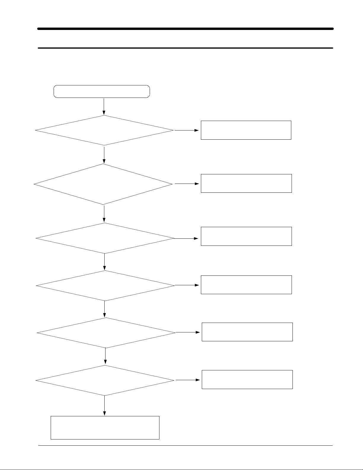
9-1.
Power On
9-1-1.
PDA Part
Insert Power
NG
Check pin4of V_BAT in
U502
is more than
Yes
Check followings
C532 is
C544 is
C540 is
1.8V
3.0V
3.0V
Yes
3.1V
:
No
No
Change the Battery&check ZD802
Check the U504
and the related cuircuit
Check C537 is
Check pin1of TR500
is'H'
Check C530, C531 is
Check pin2of U904 is'H'
1.2V
Yes
Yes
1.2V
Yes
No
No
No
No
Check the U504
and the related cuircuit
Check the UCP900
Check the U504
and the related cuircuit
Check the U904
and the related cuircuit
Yes
Check Other Power Circuit
SAMSUNG Proprietary-Contents may change without notice
This Document can not be used without Samsung's authorization
9-1
Page 2
Flow Chart of Troubleshooting
9-2
SAMSUNG Proprietary-Contents may change without notice
This Document can not be used without Samsung's authorization
Page 3
Flow Chart of Troubleshooting
9-3
SAMSUNG Proprietary-Contents may change without notice
This Document can not be used without Samsung's authorization
Page 4
Flow Chart of Troubleshooting
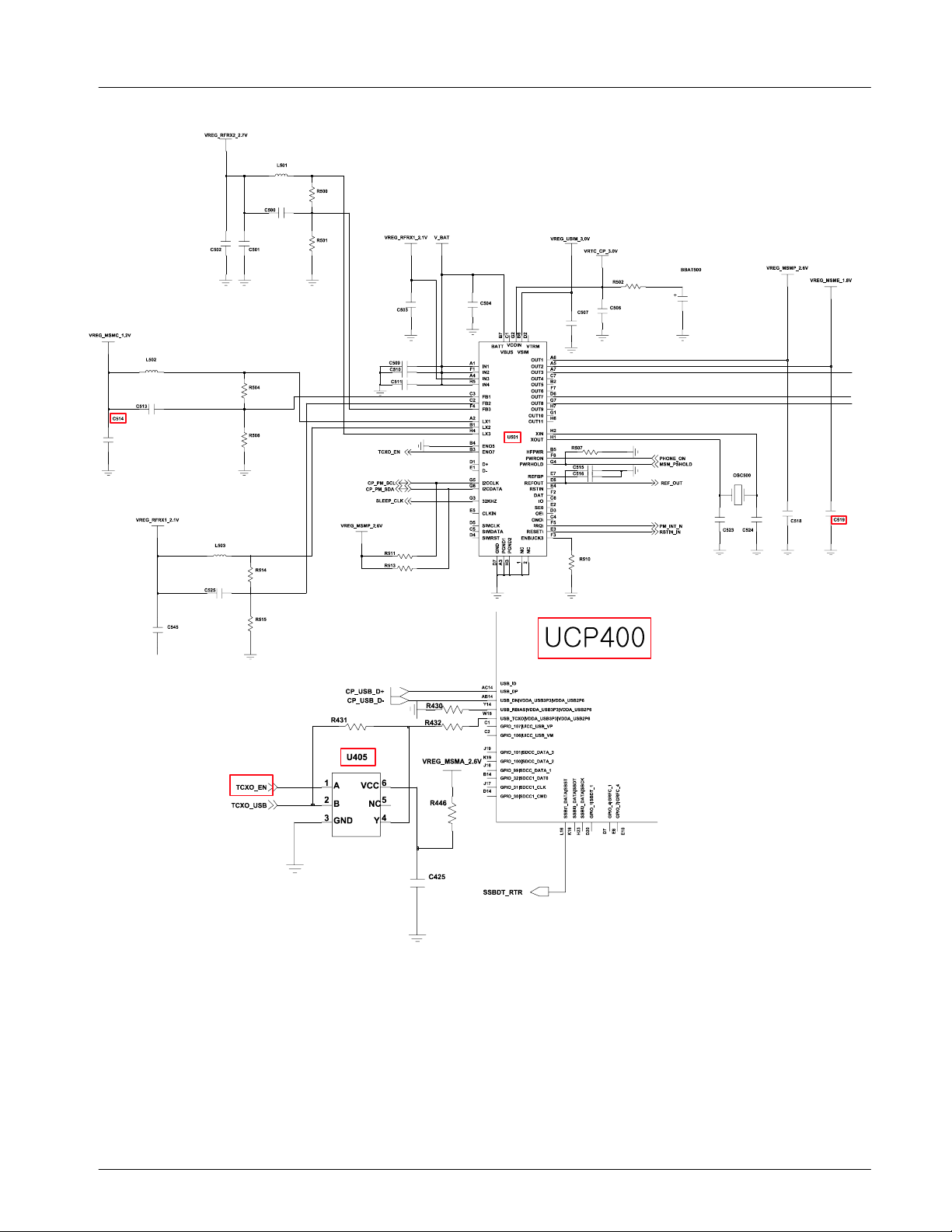
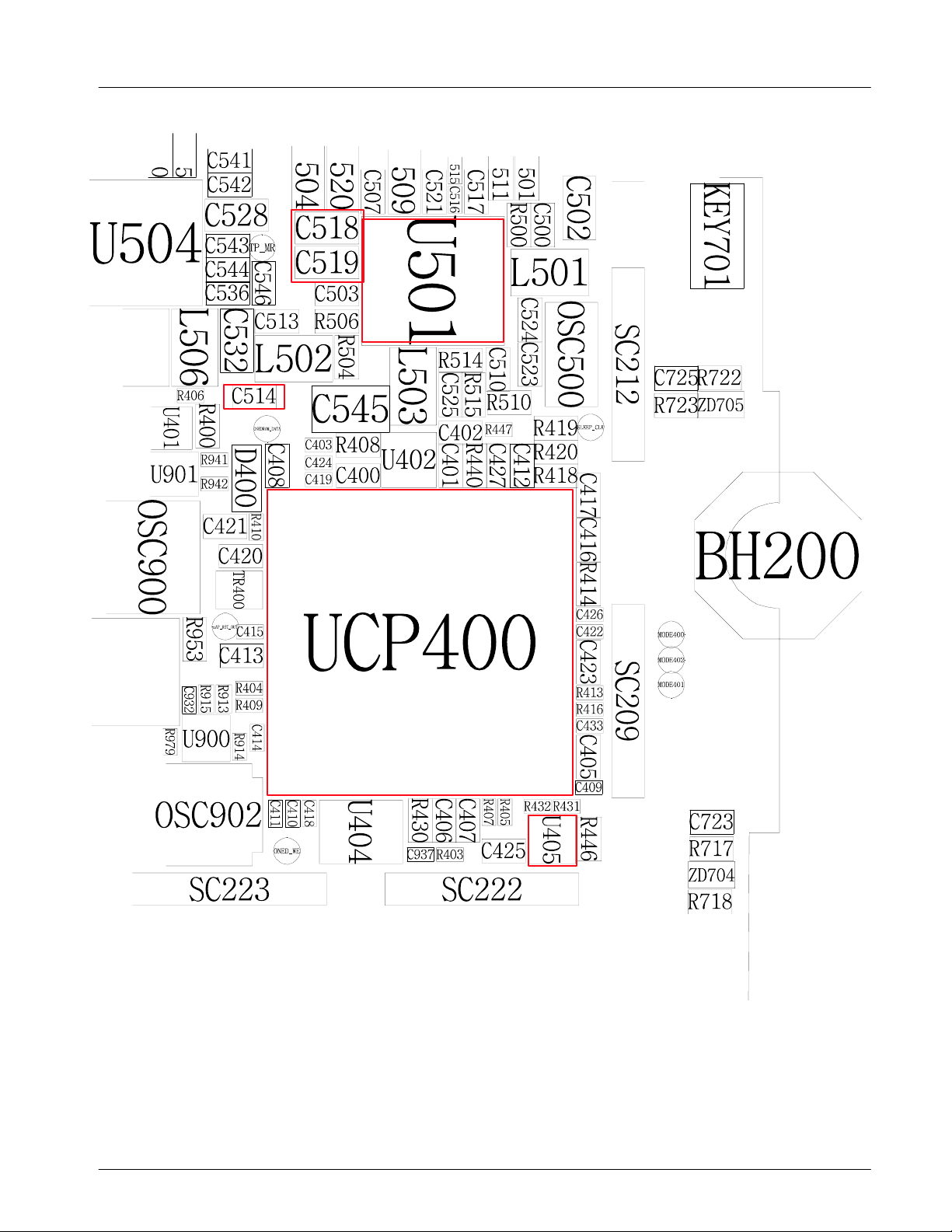
9-1-2.
Phone Part
Phone Power On'does not work
'
Yes
Check the Battery Voltage
is more than
Check followings
C514 is
C519 is
Check C518 is
Yes
1.2V
1.8V
Yes
3.5V
2.6V
No
:
No
No
Change the Battery
Check the U501
and the related cuircuit
Check the U501
Yes
Check C296 is
Check U405 Pin1is'H'
Check the initial operation
2.85V
Yes
Yes
No
No
Check the U501
Check the UCP400
and the related cuircuit
9-4
SAMSUNG Proprietary-Contents may change without notice
This Document can not be used without Samsung's authorization
Page 5
Flow Chart of Troubleshooting
9-5
SAMSUNG Proprietary-Contents may change without notice
This Document can not be used without Samsung's authorization
Page 6
Flow Chart of Troubleshooting
9-6
SAMSUNG Proprietary-Contents may change without notice
This Document can not be used without Samsung's authorization
Page 7
Flow Chart of Troubleshooting
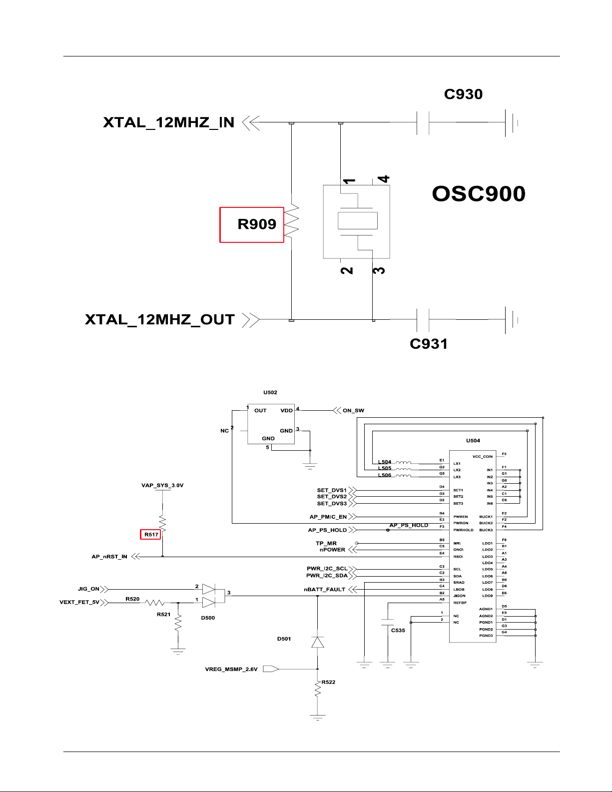
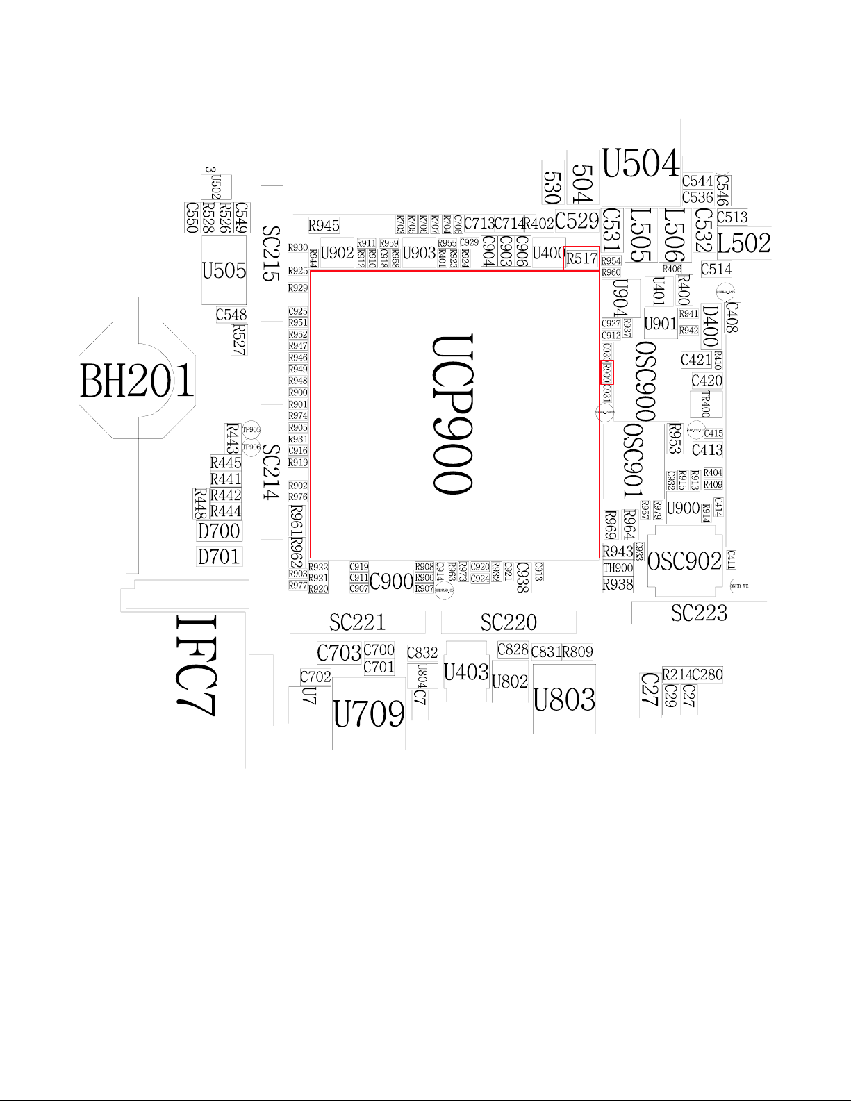
9-2.
Initial
Initial Failure
Yes
AP_nRST_IN="High"?
at R517
Yes
Check CLK
XTAL_12MHZ_IN/OUT
at
R909
Good
Check the32bit data signal
memory(UCP
&
900)
Bad
No
Check the circuit related to reset
Bad
Change OSC900
Replace PBA
END
Good
9-7
SAMSUNG Proprietary-Contents may change without notice
This Document can not be used without Samsung's authorization
Page 8
Flow Chart of Troubleshooting
9-8
SAMSUNG Proprietary-Contents may change without notice
This Document can not be used without Samsung's authorization
Page 9
Flow Chart of Troubleshooting
9-9
SAMSUNG Proprietary-Contents may change without notice
This Document can not be used without Samsung's authorization
Page 10
Flow Chart of Troubleshooting
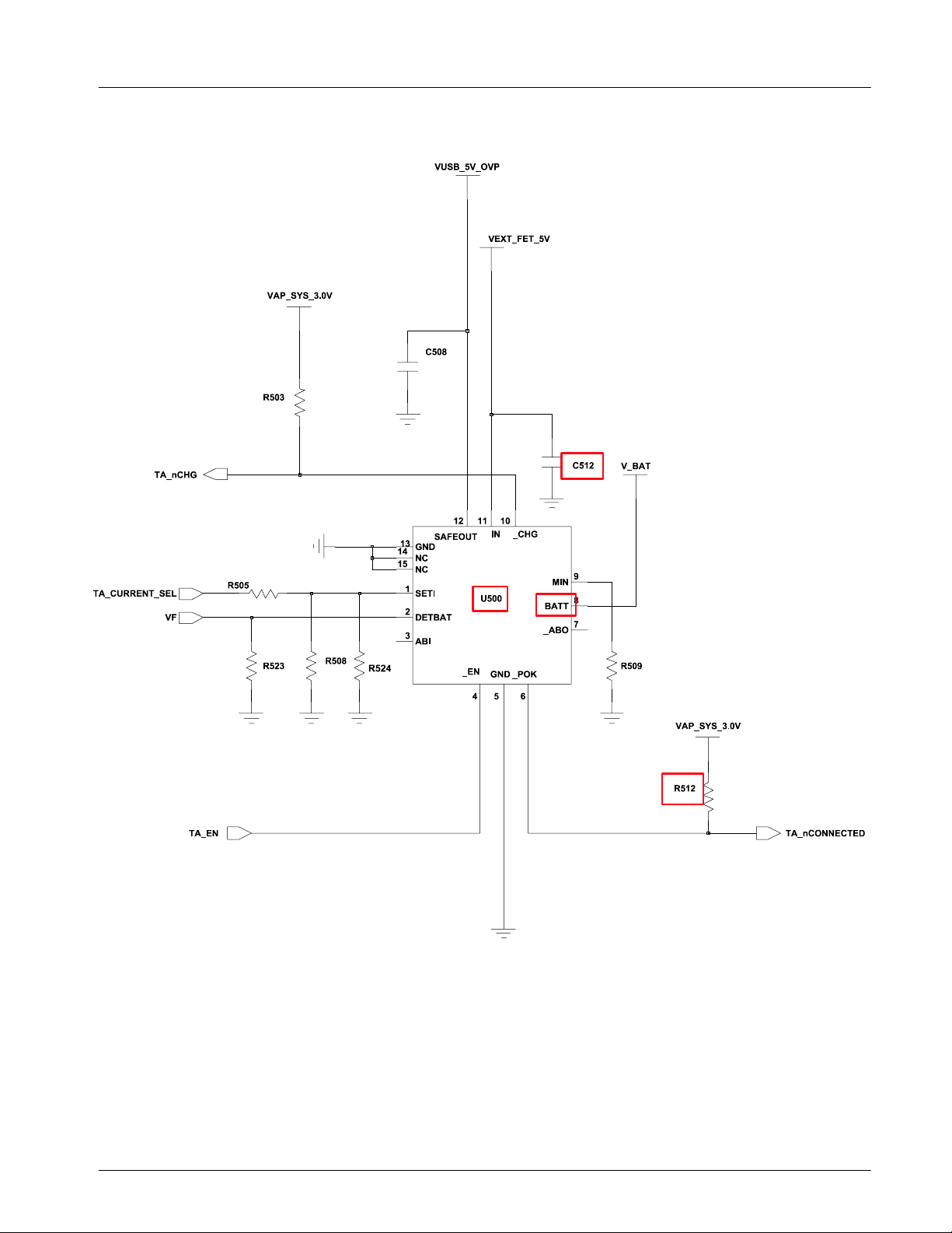
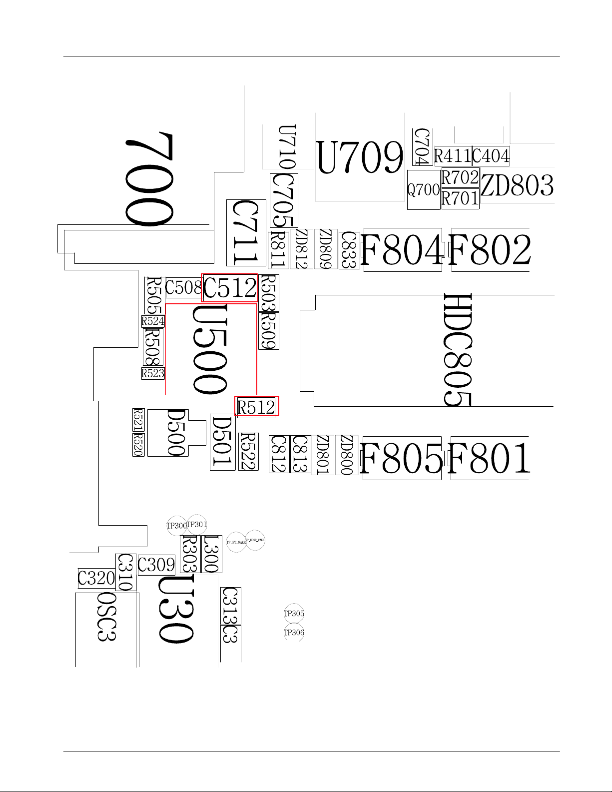
9-3.
Charging Part
Abnormal charging part
Yes
Check the C512
>4.3V
Yes
Check R512
='L'?
Yes
No
No
Check the circuit related to
VEXT_FET_5V and
Check the circuit related to
TA_nCHG signal
U500
Check the
≒
END
U500
4.2V
Yes
pin
12
No
Resolder or replace
U500
9-10
SAMSUNG Proprietary-Contents may change without notice
This Document can not be used without Samsung's authorization
Page 11
Flow Chart of Troubleshooting
9-11
SAMSUNG Proprietary-Contents may change without notice
This Document can not be used without Samsung's authorization
Page 12
Flow Chart of Troubleshooting
9-12
SAMSUNG Proprietary-Contents may change without notice
This Document can not be used without Samsung's authorization
Page 13
Flow Chart of Troubleshooting
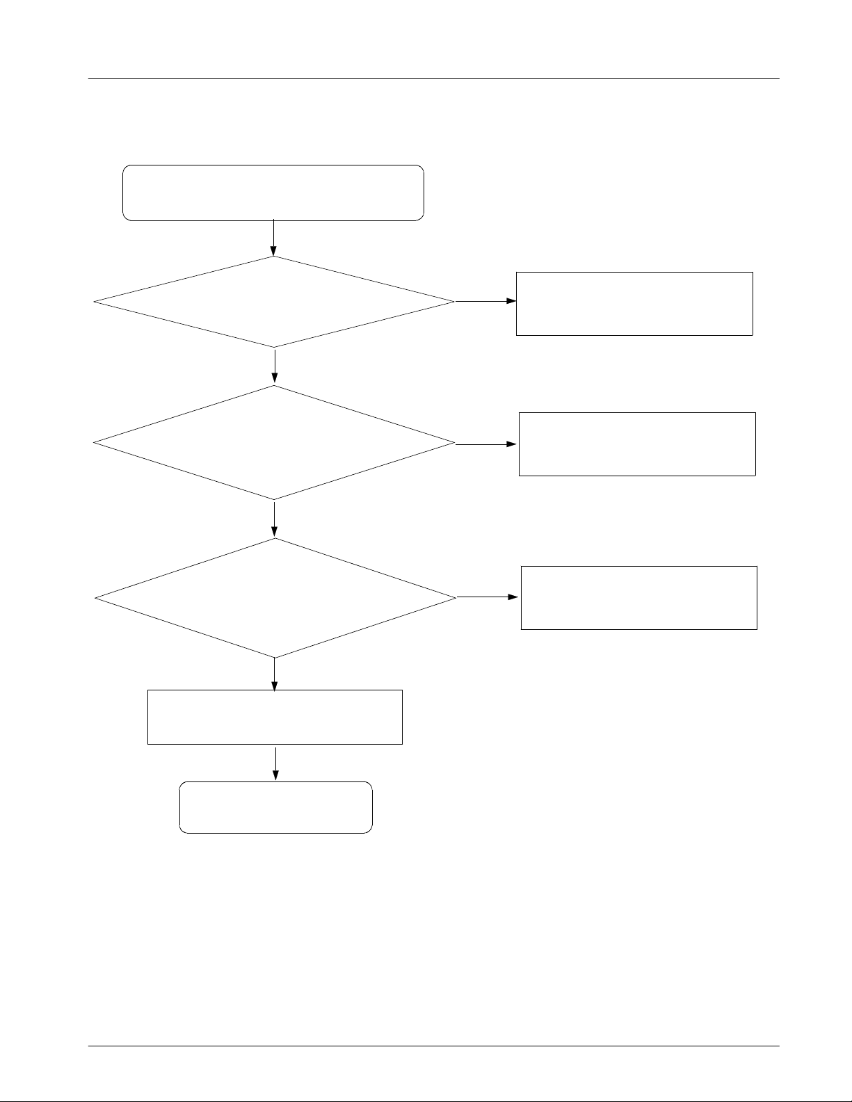
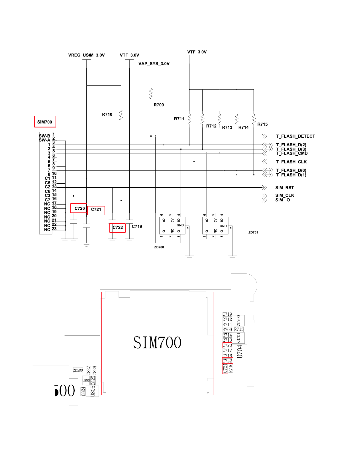
9-4.
Sim Part
Phone can't access SIM Card
Yes
C721
After Power ON,
Check SIM_CLK Signal on
pin15at SIM700
="3.0
Yes
Yes
V"?
No
No
Check the PMIC(
Check the SIM Clock
U501)
After SIM card insert,
SIM700 pin
H(SIM_RST)"?
="
Check the SIM Card
13
Yes
Yes
END
No
Resolder SIM700 or replace PBA
9-13
SAMSUNG Proprietary-Contents may change without notice
This Document can not be used without Samsung's authorization
Page 14
Flow Chart of Troubleshooting
9-14
SAMSUNG Proprietary-Contents may change without notice
This Document can not be used without Samsung's authorization
Page 15
Flow Chart of Troubleshooting
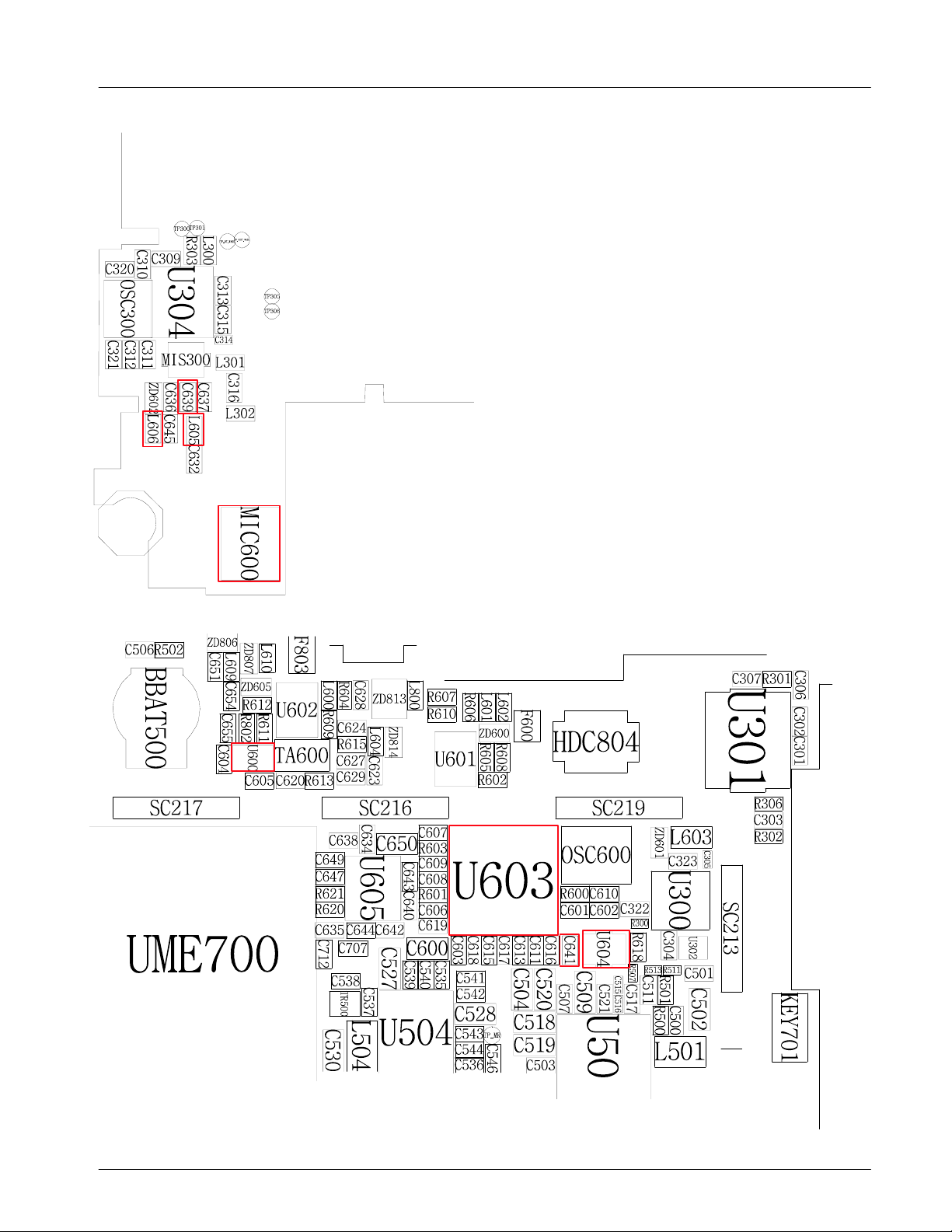
9-5-1.
Microphone Part(Main MIC)
Phone Main MIC(For Handset Call, Voice
Video Recording) does not work
YES
Check the signal
at L606, C639(MIC
Signal)
OK
Check the signal
at L605(MIC Supply)
OK
Check the signal
at C641
&
Not OK
Not OK
Not OK
Resolder L606, C639 or Resolder
esolder L605 and Check the U600
R
MIC(MIC
MIC BIAS LDO)
(
Check the U604(SPDT)
600)
Yes
Check all power source
related U603
Yes
Change the PBA
Not OK
Change the PBA
9-15
SAMSUNG Proprietary-Contents may change without notice
This Document can not be used without Samsung's authorization
Page 16
Flow Chart of Troubleshooting
VMICBIAS_2.8V
VMICBIAS_2.8V
POWER
POWER
MIC600
L605
C632
C645
C637
MAIN_MIC_P
MAIN_MIC_N
OUT
OUT
4
GND2
GND
3
GND12GND
1
L606
ZD602
C636
C639
V_BAT
MAIN_MIC_N
MAIN_MIC_P
MIC_SEL
VMICBIAS_2.8V
0
1
NO2
9
COM2
8
IN2
VCC
NC
7
R618
MIC_IN_P
1
U604
2
NO1
COM1
IN1
NC1
GND
6
C641
3
4
5
MIC_IN_N
SUB_MIC_N
SUB_MIC_P
U600
MICBIAS_EN
C604
VDD4VOUT
3
CE
GND
GND
5
VAP_SYS_3.0V
1
2
C605
VAP_SYS_3.0V
AUDIO_EN
C610
VAP_SYS_3.0V
VDD
NC|TR
34
OUT
GND
21
OSC600
C606
C607
R601
R603
C608
BT_PCM_IN
BT_PCM_OUT
BT_PCM_SYNC
C609
I2S_SDO
I2S_SDI
I2S_SYNC
AUDIO_EN
C619
C601
8
F
2
D
D
D
D
V
V
A
T
S
4
3
S
S
S
S
V
V
7
H
2
8
7
J
E
D
D
D
D
D
D
D
V
V
V
P
D
A
GPIO1
BICKA
BICKB
CSN|CAD0
CCLK|SCL
CDTI|SDA
LIN1||IN1+
LIN2|IN2+
LIN3|IN3+
LIN4|IN4+
LOUT1|RCP
LOUT2
LOUT3|LOP
RIN1|IN1RIN2|IN2RIN4|IN3RIN4|IN4-
ROUT1|RCN
ROUT2
ROUT3|LON
2
1
S
S
S
S
V
V
8
1
9
F
E
B
GPO2
BICK
CDTO
C600R600
8
A
J1
J9
J5
G8
G2
J6
H6
H8
J2
A2
A3
A4
B5
A7
B9
B6
B2
B3
B4
A5
B7
C9
A6
C603
C611
C613
C615
C616
C617
C618
I2S_SCLK
BT_PCM_CLK
FM_SCL
FM_SDA
MIC_IN_P
RADIO_L
EAR_MIC_P
MSM_SPK_P
RCV_P
CODEC_OUT_L
MSM_MIC_P
MIC_IN_N
RADIO_R
EAR_MIC_N
MSM_SPK_N
RCV_N
CODEC_OUT_R
MSM_MIC_N
C602
8
9
9
2
E
E
D
D
3
T
C
M
D
B
O
O
D
C
C
C
V
O
V
V
T
C
V
D1
SAIN1
C2
SAIN2
C1
SAIN3
I2C
MCKI
MCKO
MDT
MPWR
MUTET
SDTI
SDTIA
SDTIB
SDTO
SDTOA
SDTOB
SYNCA
SYNCB
LRCK
PDN
TEST
U603
C
C
C
N
N
N
3
2
1
C
H5
H4
J4
A1
B1
C8
H1
J8
G1
H2
G9
F2
H9
F1
J3
H3
A9
9-16
SAMSUNG Proprietary-Contents may change without notice
This Document can not be used without Samsung's authorization
Page 17
Flow Chart of Troubleshooting
9-17
SAMSUNG Proprietary-Contents may change without notice
This Document can not be used without Samsung's authorization
Page 18
Flow Chart of Troubleshooting
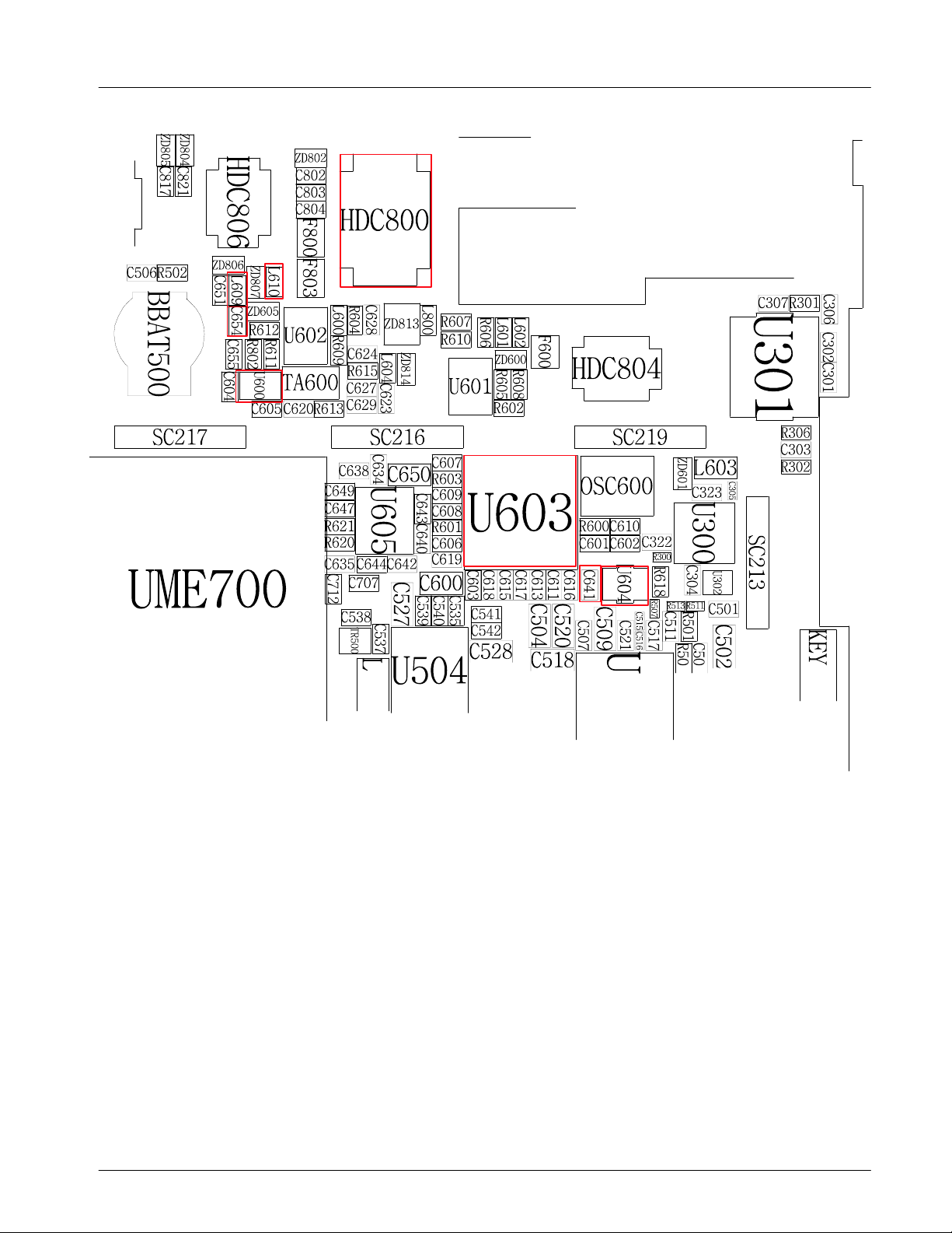
9-5-2.
Microphone Part(Sub MIC)
Phone Sub MIC(For Loud SPK Call) does not
work
YES
Check the connection
of HDC806
OK
Check the signal
at L610, C654(MIC
Signal)
OK
Check the signal
at L609(MIC Supply)
Not OK
Not OK
Not OK
Re-Connect!!
Change the Sub MIC module and
Resolder L610, C654
esolder L609 and Check the U600
R
MIC BIAS LDO)
(
Yes
Check the signal
at C641
Yes
Check all power source
related U603
Yes
Change the PBA
Not OK
Check the U604(SPDT)
Not OK
Change the PBA
9-18
SAMSUNG Proprietary-Contents may change without notice
This Document can not be used without Samsung's authorization
Page 19

Flow Chart of Troubleshooting
9-19
SAMSUNG Proprietary-Contents may change without notice
This Document can not be used without Samsung's authorization
Page 20
Flow Chart of Troubleshooting
9-20
SAMSUNG Proprietary-Contents may change without notice
This Document can not be used without Samsung's authorization
Page 21
Flow Chart of Troubleshooting
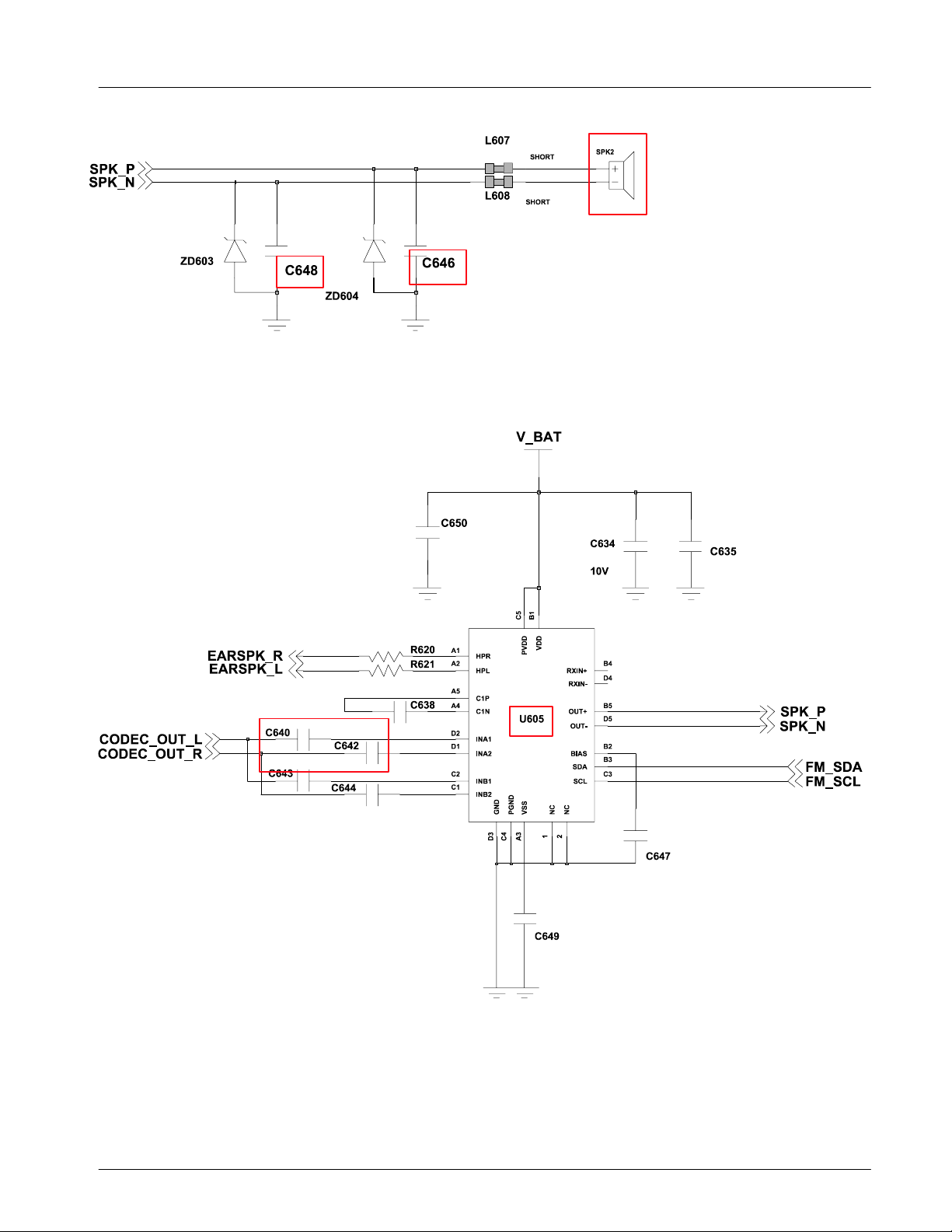
9-6.
Speaker Part(Melody)
Speaker does not work
Yes
Check the Speaker FPCB
and Speaker Module
Yes
Check the signal at
C640, C642
Yes
No
No
Replace the Speaker Module
Check all power source
related U603
No
Change the PBA
Check the signal at
C648, C646
Yes
Replace the Speaker Module
No
Check the U605 and Resolder the U605
9-21
SAMSUNG Proprietary-Contents may change without notice
This Document can not be used without Samsung's authorization
Page 22
Flow Chart of Troubleshooting
9-22
SAMSUNG Proprietary-Contents may change without notice
This Document can not be used without Samsung's authorization
Page 23
Flow Chart of Troubleshooting
9-23
SAMSUNG Proprietary-Contents may change without notice
This Document can not be used without Samsung's authorization
Page 24
Flow Chart of Troubleshooting
9-7.
Receiver Part
Receiver does not work
Check the connection
of HDC806
Check the signal at
ZD804, ZD805 of HDC806
Does it work?
Yes
Yes
Yes
No
No
No
Replace the Receiver Module
Check all power source
andresolder oreplace U603
related U603
Change the PBA
END
Yes
9-24
SAMSUNG Proprietary-Contents may change without notice
This Document can not be used without Samsung's authorization
Page 25

Flow Chart of Troubleshooting
9-25
SAMSUNG Proprietary-Contents may change without notice
This Document can not be used without Samsung's authorization
Page 26

Flow Chart of Troubleshooting
9-26
SAMSUNG Proprietary-Contents may change without notice
This Document can not be used without Samsung's authorization
Page 27

Flow Chart of Troubleshooting
9-8.
Key Data Input
Check Initial Operation
When one of the keys is
is it displayed on LCD?
When one of the keys is
KEY_IO signal is OK?
pushed,
pushed,
Yes
No
Check the Key FPCB
Yes
No
Replace the PBA
Yes
END
9-27
SAMSUNG Proprietary-Contents may change without notice
This Document can not be used without Samsung's authorization
Page 28

Flow Chart of Troubleshooting
9-28
SAMSUNG Proprietary-Contents may change without notice
This Document can not be used without Samsung's authorization
Page 29

I
F
C
7
0
0
R
5
0
5
R524
R
5
0
8
R523
R
5
2
1
R
5
2
0
C508
U
5
0
0
D
5
0
0
C
7
1
1
C512
R512
D
5
R
5
0
2
1
2
R
5
0
3
R
5
0
9
C702
U
7
1
0
C
7
0
5
R
8
1
1
C
8
1
2
C703
Z
D
8
1
2
C
8
1
3
C700
C701
U709
Z
C
D
8
8
3
0
3
9
Z
Z
D
D
8
8
0
0
1
0
F805
C832
U
8
0
4
C
7
0
4
Q700
R411
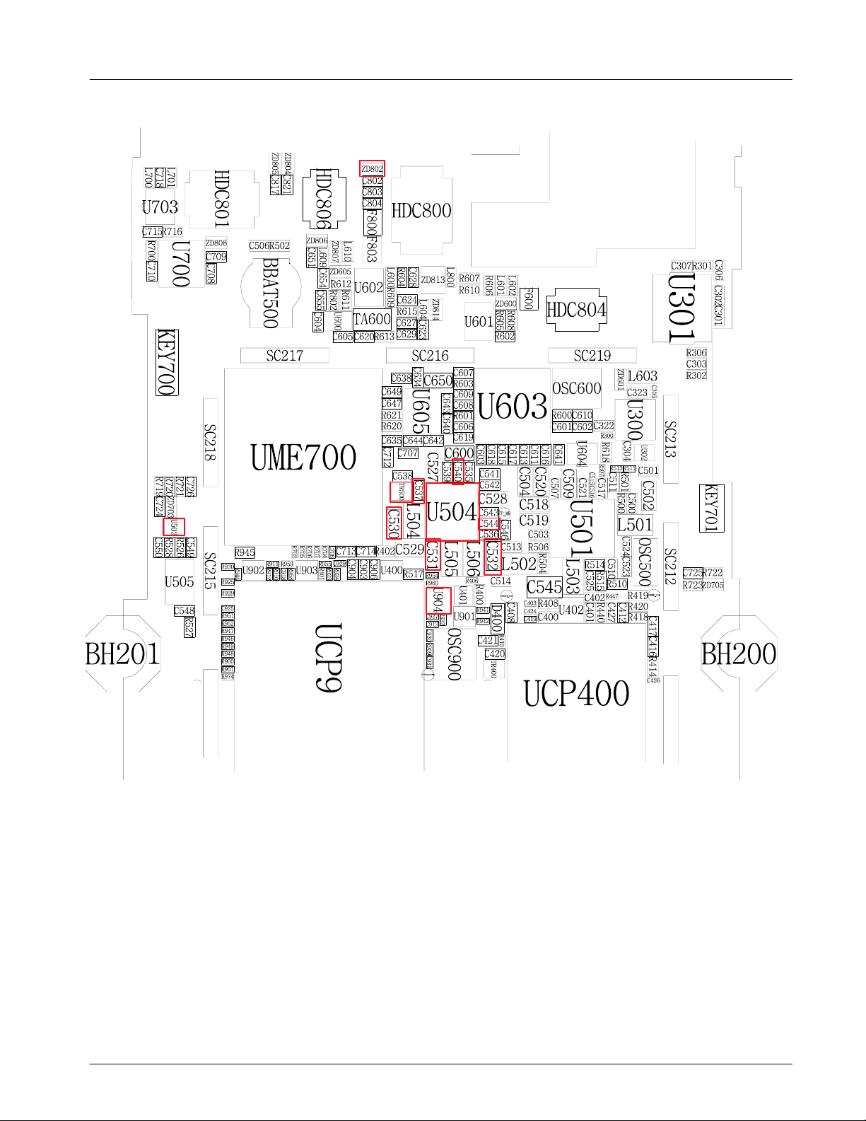
SC220SC221
U403
C404
R702
ZD803
R701
F802F804
H
D
C
8
0
5
F801
C828
U802
C829
R810
R
8
0
8
F806
C831
R809
U803
L801
R
8
C830
0
7
R804
C800
Flow Chart of Troubleshooting
C320
O
S
C
3
0
0
C
C
3
3
1
2
2
1
C
3
1
0
C
3
1
1
Z
D
6
0
2
L
6
0
6
C309
TP301
TP300
L
R
3
3
0
0
0
3
U
3
0
4
MIS300
C
C
C
6
6
6
3
3
3
6
7
9
C
L
6
6
4
0
5
5
C
6
3
2
TP_BT_WAKE
C
3
1
3
C
3
1
5
C314
L301
C
3
1
6
L302
TP_HOST_WAKE
TP305
TP306
9-29
SAMSUNG Proprietary-Contents may change without notice
This Document can not be used without Samsung's authorization
Page 30

Flow Chart of Troubleshooting
9-9.
Back Light(for Color Main LCD)
Back light does not work
Yes
Is LCD Contrast set on high
level in the Menu?
Yes
C542, C829
=3.0
Yes
V?
No
No
Set LCD Contrast on high level
Check or replace the U504,
U802
C830
Replace the LCD Module
=18
END
V?
Yes
Yes
No
Check the
U803
9-30
SAMSUNG Proprietary-Contents may change without notice
This Document can not be used without Samsung's authorization
Page 31

Flow Chart of Troubleshooting
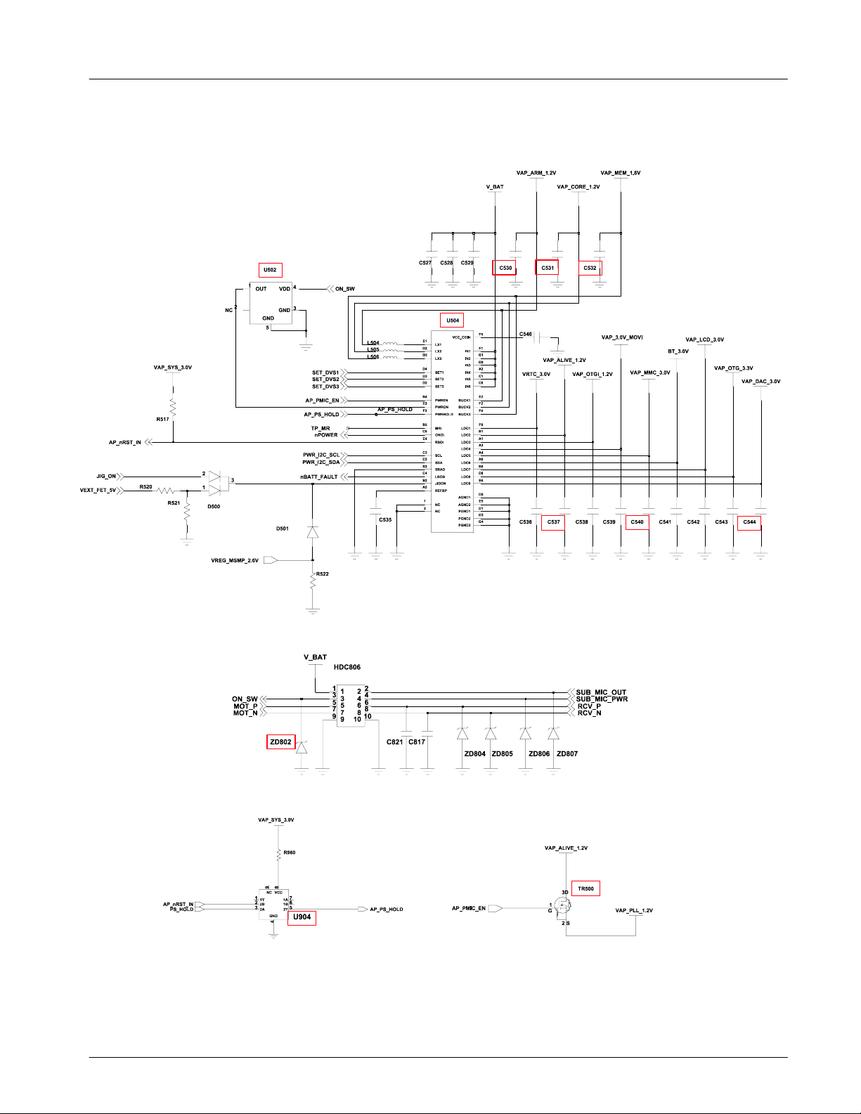
JIG_ON
VEXT_FET_5V
AP_nRST_IN
R520
VAP_SYS_3.0V
R517
R521
2
1
D500
VREG_MSMP_2.6V
VAP_CORE_1.2V
C532C531
VAP_OTGI_1.2V
C538 C542C537
VAP_MEM_1.8V
VAP_3.0V_MOVI
C539
VAP_MMC_3.0V
C540
VAP_LCD_3.0V
BT_3.0V
VAP_OTG_3.3V
VAP_DAC_3.0V
C543
C541C536
C544
VAP_ARM_1.2V
V_BAT
C528
C527
C529
U502
1
4
OUT VDD
2
GND
NC
GND
5
3
D501
3
AP_PMIC_EN
AP_PS_HOLD
PWR_I2C_SCL
PWR_I2C_SDA
nBATT_FAULT
SET_DVS1
SET_DVS2
SET_DVS3
TP_MR
nPOWER
ON_SW
L504
L505
L506
AP_PS_HOLD
C535
E1
G2
G5
D4
D3
D2
B4
E3
F3
B5
C5
E4
C3
C2
B3
C4
B2
A5
1
2
U504
VCC_COIN
LX1
LX2
LX3
SET1
SET2
SET3
PWREN
PWRON
PWRHOLDF4BUCK3
MR\
ONO\
RSO\
SCL
SDA
SRAD
LBOB
JIGON
REFBP
NC
NC
C530
F5
C546
F1
IN1
G1
IN2
G6
IN3
A2
IN4
C1
IN5
C6
IN6
E2
BUCK1
F2
BUCK2
F6
LDO1
B1
LDO2
A1
LDO3
A3
LDO4
A4
LDO5
A6
LDO6
B6
LDO7
D6
LDO8
E6
LDO9
D5
AGND1
E5
AGND2
D1
PGND1
G3
PGND2
G4
PGND3
VAP_ALIVE_1.2V
VRTC_3.0V
R522
LED_DRV_EN
LED_DRV_SEL
R809
V_BAT
C831
U803
1
PVIN
2
EN|SET
3
SEL
4
VIN
5
NC
6
SW SW
OVP
AGND
PGND
V_BAT
L801
12
LIN
11
10
FB
R807
9
8
7
ZD803
R808
LED_VOUT_18V
LCD_ENLED_VOUT_FB
C828
C830
U802
1
VOUT1
VIN
2
GND
VOUT2
3
EN2
GND
7
VLCD_3.0V
6
5
4
EN1
C829
R810
9-31
SAMSUNG Proprietary-Contents may change without notice
This Document can not be used without Samsung's authorization
Page 32

Flow Chart of Troubleshooting
9-32
SAMSUNG Proprietary-Contents may change without notice
This Document can not be used without Samsung's authorization
Page 33

Flow Chart of Troubleshooting
9-10.
Camera part
Camera" function does not work
"
(3M
Check the Camera
pin
&
Check CAM_MCLK,
CAMERA)
Yes
connector
Yes
HCD800
4,6,5 = 2.8
pin
3=1.8
Yes
CAM_PCLK
Working?
V?
V?
No
No
No
Reconnect the camera module
Check HDC800
Check HDC800
, U805, U806
Yes
Check pin
Working properly?
Does lt looking good
Is there another problem?
Replace the camera
2, 8, 10, 12
Yes
?
Yes
Yes
module
No
CheckUCP900
Check F800,F803
END
9-33
SAMSUNG Proprietary-Contents may change without notice
This Document can not be used without Samsung's authorization
Page 34

Flow Chart of Troubleshooting
9-34
SAMSUNG Proprietary-Contents may change without notice
This Document can not be used without Samsung's authorization
Page 35

Flow Chart of Troubleshooting
9-35
SAMSUNG Proprietary-Contents may change without notice
This Document can not be used without Samsung's authorization
Page 36

Flow Chart of Troubleshooting
9-10.
Camera part(CIF CAMERA)
Camera" function does not work
"
Yes
Check the Camera
connector
Yes
HDC801
pin
2, 6 = 2.8
pin
&
Check CAM_MCLK,
CAM_PCLK
Working?
4=1.8
Yes
V?
V?
No
Reconnect the camera module
No
Check HDC801, U805, U806
No
Check HDC801
Yes
Check pin
Working properly?
Does lt looking good
Is there another problem?
Replace the camera
1, 3, 17, 21
Yes
?
Yes
Yes
module
No
CheckUCP900
Check F800, F803
END
9-36
SAMSUNG Proprietary-Contents may change without notice
This Document can not be used without Samsung's authorization
Page 37

Flow Chart of Troubleshooting
9-37
SAMSUNG Proprietary-Contents may change without notice
This Document can not be used without Samsung's authorization
Page 38

Flow Chart of Troubleshooting
9-38
SAMSUNG Proprietary-Contents may change without notice
This Document can not be used without Samsung's authorization
Page 39

Flow Chart of Troubleshooting
9-11.
GSM850 Receiver
RX ON
RF input
Amp
PAM200 Pin
>= -65
PAM200 Pin
>= -68
pin
50 >= -70
pin
51 >= -70
: 190
:-50
U200
dBm
Yes
dBm
Yes
dBm
Yes
CH
8
4
dBm
dBm
No
No
Resolder RFS200,C200, C204, L201
Check PAM200
pin
Resolder or change
F200,C210,C211,L202,L203
27 =
pin
L, pin28=H
1=H
Yes
NoNo
Check ANT Switch
control circuit
Resolder PAM200
Yes
U200 pin
Check UCP400
>= 1V
END
1,3,23
Yes
No
Check all voltage
sources of U200
Is it OK?
Yes
No
Check&Resolder
CP PMIC(U501)
Resolder U200
9-39
SAMSUNG Proprietary-Contents may change without notice
This Document can not be used without Samsung's authorization
Page 40

Flow Chart of Troubleshooting
9-40
SAMSUNG Proprietary-Contents may change without notice
This Document can not be used without Samsung's authorization
Page 41

Flow Chart of Troubleshooting
9-41
SAMSUNG Proprietary-Contents may change without notice
This Document can not be used without Samsung's authorization
Page 42

Flow Chart of Troubleshooting
9-12.
GSM850 Transmitter
TX ON(5Level)
Yes
PAM200 Pin
>= 20
PAM200 Pin
>=5.5
U200 pin
>= -5.5
dBm
No
dBm
No
dBm
8
23
55
Yes
Yes
Resolder RFS200,C200, C204, L201
Check PAM200
pin
Resolder or change
C243,R205,R207,R208
27 =
pin
H, pin28=L
1=L
Yes
NoYes
Check ANT Switch
control circuit
Resolder PAM200
No
U200 pin
Check UCP400
1,3,23
>= 1V
Yes
END
No
Check all voltage
sources of U200
Is it OK?
Yes
No
Check&Resolder
CP PMIC(U501)
Resolder U200
9-42
SAMSUNG Proprietary-Contents may change without notice
This Document can not be used without Samsung's authorization
Page 43

Flow Chart of Troubleshooting
9-43
SAMSUNG Proprietary-Contents may change without notice
This Document can not be used without Samsung's authorization
Page 44

Flow Chart of Troubleshooting
9-44
SAMSUNG Proprietary-Contents may change without notice
This Document can not be used without Samsung's authorization
Page 45

Flow Chart of Troubleshooting
9-13.
GSM900 Receiver
RX ON
RF input
Amp
PAM200 Pin
>= -65
PAM200 Pin
>= -68
pin
49 >= -70
pin
48 >= -70
: 190
:-50
U200
dBm
Yes
dBm
Yes
dBm
Yes
CH
8
5
dBm
dBm
No
No
Resolder RFS200,C200, C204, L201
Check PAM200
pin
Resolder or change
F201,C216,C217,L204,L205
27 =
pin
H, pin28=H
1=H
Yes
NoNo
Check ANT Switch
control circuit
Resolder PAM200
Yes
U200 pin
Check UCP400
>= 1V
END
1,3,23
Yes
No
Check all voltage
sources of U200
Is it OK?
Yes
No
Check&Resolder
CP PMIC(U501)
Resolder U200
9-45
SAMSUNG Proprietary-Contents may change without notice
This Document can not be used without Samsung's authorization
Page 46

Flow Chart of Troubleshooting
9-46
SAMSUNG Proprietary-Contents may change without notice
This Document can not be used without Samsung's authorization
Page 47

Flow Chart of Troubleshooting
9-47
SAMSUNG Proprietary-Contents may change without notice
This Document can not be used without Samsung's authorization
Page 48

Flow Chart of Troubleshooting
9-14.
GSM900 Transmitter
TX ON(5Level)
Yes
PAM200 Pin
>= 20
PAM200 Pin
>=5.5
U200 pin
>= -5.5
dBm
No
dBm
No
dBm
8
23
55
Yes
Yes
Resolder RFS200,C200, C204, L201
Check PAM200
pin
Resolder or change
C243,R205,R207,R208
27 =
pin
H, pin28=L
1=L
Yes
NoYes
Check ANT Switch
control circuit
Resolder PAM200
No
U200 pin
Check UCP400
1,3,23
>= 1V
Yes
END
No
Check all voltage
sources of U200
Is it OK?
Yes
No
Check&Resolder
CP PMIC(U501)
Resolder U200
9-48
SAMSUNG Proprietary-Contents may change without notice
This Document can not be used without Samsung's authorization
Page 49

Flow Chart of Troubleshooting
9-49
SAMSUNG Proprietary-Contents may change without notice
This Document can not be used without Samsung's authorization
Page 50

Flow Chart of Troubleshooting
9-50
SAMSUNG Proprietary-Contents may change without notice
This Document can not be used without Samsung's authorization
Page 51

Flow Chart of Troubleshooting
9-15.
DCS1800 Receiver
RX ON
RF input
Amp
PAM200 Pin
>= -65
PAM200 Pin
>= -68
pin
47 >= -70
pin
46 >= -70
: 190
:-50
U200
dBm
Yes
dBm
Yes
dBm
Yes
Yes
CH
8
6
dBm
dBm
No
No
Resolder RFS200,C200, C204, L201
Check PAM200
pin
Resolder or change
F203,C224,L207,L208,L209
27 =
pin
H, pin28=
1=H
L
Yes
NoNo
Check ANT Switch
control circuit
Resolder PAM200
U200 pin
Check UCP400
>= 1V
END
1,3,23
Yes
No
Check all voltage
sources of U200
Is it OK?
Yes
No
Check&Resolder
CP PMIC(U501)
Resolder U200
9-51
SAMSUNG Proprietary-Contents may change without notice
This Document can not be used without Samsung's authorization
Page 52

Flow Chart of Troubleshooting
9-52
SAMSUNG Proprietary-Contents may change without notice
This Document can not be used without Samsung's authorization
Page 53

Flow Chart of Troubleshooting
9-53
SAMSUNG Proprietary-Contents may change without notice
This Document can not be used without Samsung's authorization
Page 54

Flow Chart of Troubleshooting
9-16.
DCS1800 Transmitter
TX ON(5Level)
Yes
PAM200 Pin
>= 20
PAM200 Pin
>=5.5
U200 pin
>= -5.5
dBm
No
dBm
No
dBm
8
21
56
Yes
Yes
Resolder RFS200,C200, C204, L201
Check PAM200
pin
Resolder or change
C243,R201,R202,R203
27 =
H, pin28=
pin
1=L
H
Yes
NoYes
Check ANT Switch
control circuit
Resolder PAM200
No
U200 pin
Check UCP400
>= 1V
END
1,3,23
Yes
No
Check all voltage
sources of U200
Is it OK?
Yes
No
Check&Resolder
CP PMIC(U501)
Resolder U200
9-54
SAMSUNG Proprietary-Contents may change without notice
This Document can not be used without Samsung's authorization
Page 55

Flow Chart of Troubleshooting
9-55
SAMSUNG Proprietary-Contents may change without notice
This Document can not be used without Samsung's authorization
Page 56

Flow Chart of Troubleshooting
9-56
SAMSUNG Proprietary-Contents may change without notice
This Document can not be used without Samsung's authorization
Page 57

Flow Chart of Troubleshooting
9-17.
PCS1900 Receiver
RX ON
RF input
Amp
PAM200 Pin
>= -65
PAM200 Pin
>= -68
pin
45 >= -70
pin
44 >= -70
: 190
:-50
U200
dBm
Yes
dBm
Yes
dBm
Yes
CH
8
7
dBm
dBm
No
No
Resolder RFS200,C200, C204, L201
Check PAM200
pin
Resolder or change
F204,C227,L212,L213,L214
27 =
pin
L, pin28=
1=H
L
Yes
NoNo
Check ANT Switch
control circuit
Resolder PAM200
Yes
U200 pin
Check UCP400
>= 1V
END
1,3,23
Yes
No
Check all voltage
sources of U200
Is it OK?
Yes
No
Check&Resolder
CP PMIC(U501)
Resolder U200
9-57
SAMSUNG Proprietary-Contents may change without notice
This Document can not be used without Samsung's authorization
Page 58

Flow Chart of Troubleshooting
9-58
SAMSUNG Proprietary-Contents may change without notice
This Document can not be used without Samsung's authorization
Page 59

Flow Chart of Troubleshooting
9-59
SAMSUNG Proprietary-Contents may change without notice
This Document can not be used without Samsung's authorization
Page 60

Flow Chart of Troubleshooting
9-18.
PCS1900 Transmitter
TX ON(5Level)
Yes
PAM200 Pin
>= 20
PAM200 Pin
>=5.5
U200 pin
>= -5.5
dBm
No
dBm
No
dBm
8
21
56
Yes
Yes
Resolder RFS200,C200, C204, L201
Check PAM200
pin
Resolder or change
C243,R201,R202,R203
27 =
H, pin28=
pin
1=L
H
Yes
NoYes
Check ANT Switch
control circuit
Resolder PAM200
No
U200 pin
Check UCP400
>= 1V
END
1,3,23
Yes
No
Check all voltage
sources of U200
Is it OK?
Yes
No
Check&Resolder
CP PMIC(U501)
Resolder U200
9-60
SAMSUNG Proprietary-Contents may change without notice
This Document can not be used without Samsung's authorization
Page 61

Flow Chart of Troubleshooting
9-61
SAMSUNG Proprietary-Contents may change without notice
This Document can not be used without Samsung's authorization
Page 62

Flow Chart of Troubleshooting
9-62
SAMSUNG Proprietary-Contents may change without notice
This Document can not be used without Samsung's authorization
Page 63

Flow Chart of Troubleshooting
9-19.
**
WCDMA2100Receiver
If you check the tx chain,
Check the not only RF Device but also resistor, inductor and capacitor.
Continous Rx ON
RF Input
Amplitude
: 10700
:-50
CH
dBm
Yes
No
Normal Condition
Catch the channel?
Yes
No
Check C298
=-56
dBm?
Check Antenna Contact
Check RFS200 or
PAM200
the method like GSM)
(
Yes
Check C299
=-59
dBm?
Yes
Resolder U200 or Change
The End
No
Replace F206
9-63
SAMSUNG Proprietary-Contents may change without notice
This Document can not be used without Samsung's authorization
Page 64

Flow Chart of Troubleshooting
9-64
SAMSUNG Proprietary-Contents may change without notice
This Document can not be used without Samsung's authorization
Page 65

Flow Chart of Troubleshooting
9-65
SAMSUNG Proprietary-Contents may change without notice
This Document can not be used without Samsung's authorization
Page 66

Flow Chart of Troubleshooting
9-20.
**
WCDMA2100Transmitter
If you check the tx chain,
Check the not only RF Device but also resistor, inductor and capacitor.
Tx ON
Battery Voltage:
AGC for23dBm)
(
3.8V
Yes
No
Check C241
dBm
=8
?
Yes
Check C222
dBm?
=5
No
Yes
Check L201
dBm?
=26
No
Check the U200
Replace F202
Replace PAM201
Check C298
=24
dBm
Check L200
=23
dBm
The End
Yes
?
Yes
?
Yes
No
No
Replace F206
Check RFS200 or
PAM200, R200
the method like GSM)
(
9-66
SAMSUNG Proprietary-Contents may change without notice
This Document can not be used without Samsung's authorization
Page 67

Flow Chart of Troubleshooting
9-67
SAMSUNG Proprietary-Contents may change without notice
This Document can not be used without Samsung's authorization
Page 68

Flow Chart of Troubleshooting
9-68
SAMSUNG Proprietary-Contents may change without notice
This Document can not be used without Samsung's authorization
Page 69

Flow Chart of Troubleshooting
9-21.
FM Radio Part
FM Radio does not work
Check the connection
with the Earphone.
Is it good
the U300 Pin
Is it good
Battery Voltage)
(
Check
Yes
?
Yes
14,10
?
Yes
No
Insert the Earphone
No
Check the Battery and near circuit.
Check from C323
to EAR_JACK Module Pin
Is it OK?
Yes
Check the C611,C616
Is there signal?
Yes
4
No
Replace ZD601,L603
No
Replace the U300
9-69
SAMSUNG Proprietary-Contents may change without notice
This Document can not be used without Samsung's authorization
Page 70

Flow Chart of Troubleshooting
9-70
SAMSUNG Proprietary-Contents may change without notice
This Document can not be used without Samsung's authorization
Page 71

Flow Chart of Troubleshooting
9-71
SAMSUNG Proprietary-Contents may change without notice
This Document can not be used without Samsung's authorization
Page 72

Flow Chart of Troubleshooting
9-22.
GPS Part
Check the U301 Pin
GPS does not work
Yes
Is there signal?
Yes
U301 Pin
12 = 2.7V ?
Yes
10
No
Check the UCP400
No
Check the U501(PMIC)
heck the U301 Pin
C
Is there signal?
heck the U301 Pin
C
Is there signal?
Check the R301
Yes
7
1
No
No
Check the U200
Check the U301
Replace the R301
9-72
SAMSUNG Proprietary-Contents may change without notice
This Document can not be used without Samsung's authorization
Page 73

Flow Chart of Troubleshooting
9-73
SAMSUNG Proprietary-Contents may change without notice
This Document can not be used without Samsung's authorization
Page 74

Flow Chart of Troubleshooting
9-23.
BLUETOOTH
Operate Bluetooth
Yes
Can Bluetooth be ON?
Check L301,C316,
L302
No
abnormal
Check Voltage
1.2
V?
L300
NoYes
Resolder L301,C316,L302
Yes
normal
Check the Antenna
normal
Replace U304
The End
abnormal
Yes
Replace Antenna
while trying
BLUETOOTH on
C320=26MHz?
NO
Resolder OSC300 and
Neighboring Circuits
9-74
SAMSUNG Proprietary-Contents may change without notice
This Document can not be used without Samsung's authorization
Page 75

Flow Chart of Troubleshooting
9-75
SAMSUNG Proprietary-Contents may change without notice
This Document can not be used without Samsung's authorization
Page 76

Flow Chart of Troubleshooting
9-76
SAMSUNG Proprietary-Contents may change without notice
This Document can not be used without Samsung's authorization
Page 77

Block Diagrams
7.
7-1
SAMSUNG Proprietary-Contents may change without notice
This Document can not be used without Samsung's authorization
Page 78

PCB Diagrams
8.
Top
8-1
SAMSUNG Proprietary-Contents may change without notice
This Document can not be used without Samsung's authorization
Page 79

PCB Diagrams
Bottom
8-2
SAMSUNG Proprietary-Contents may change without notice
This Document can not be used without Samsung's authorization
 Loading...