

Page 1

PLASMA DISPLAY TV
Chassis : D52A
Model: HPL63H1X/XAA
PLASMA DISPLAY TV CONTENTS
Precautions
Reference Information
Specifications
Exploded View and Parts List
Alignment and Adjustments
Circuit Operation Description
Troubleshooting
Handling Description
Glossary
Schematic Diagrams
1.
2.
3.
4.
5.
6.
7.
8.
9.
10.
Page 2

ELECTRONICS
© Samsung Electronics Co., Ltd. JAN. 2003
Printed in Korea
AA82-00355A
Page 3
1. Precautions
1-1 Safety Precautions
1. Be sure that all of the built-in protective
devices are replaced. Restore any missing
protective shields.
2. When reinstalling the chassis and its
assemblies, be sure to restore all protective
devices, including: nonmetallic control knobs
and compartment covers.
3. Make sure that there are no cabinet openings
through which people—particularly
children—might insert fingers and contact
dangerous voltages. Such openings include
the spacing between fornt cabinet and back
cabinet, excessively wide cabinet
ventilation slots, and improperly fitted back
covers.
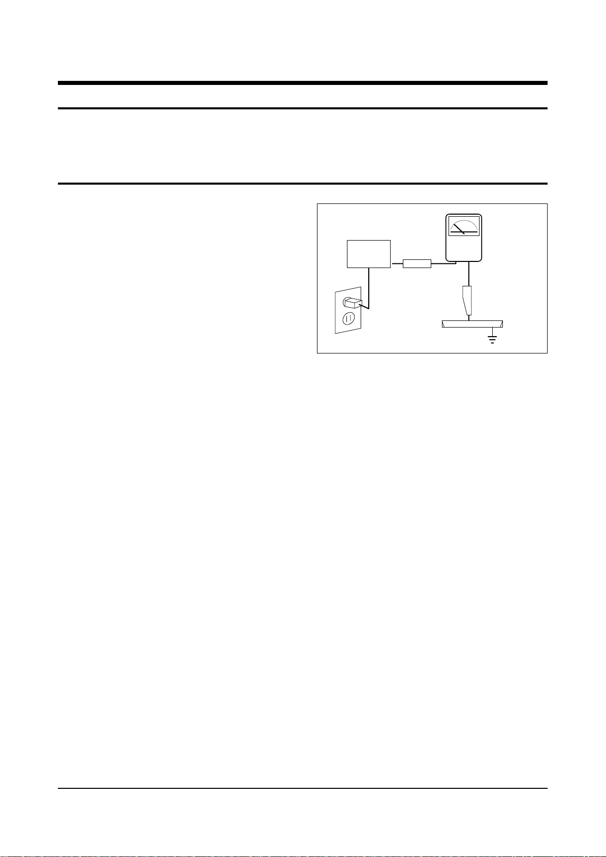
4. Leakage Current Hot Check (Figure 1-1):
Warning: Do not use an isolation
transformer during this test. Use a leakagecurrent tester or a metering system that
complies with American National Standards
Institute (ANSI C101.1, Leakage Current for
Appliances), and Underwriters Laboratories
(UL Publication UL1950.5.2).
5. With the unit completely reassembled, plug
the AC line cord directly into the power
outlet. With the unit’s AC switch first in the
ON position and then OFF, measure the
current between a known earth ground (metal
water pipe, conduit, etc.) and all exposed
metal parts, including: antennas, handle
brackets, metal cabinets, screwheads and
control shafts. The current measured should
not exceed 3.5 milliamp. Reverse the powerplug prongs in the AC outlet and repeat the
test.
Fig. 1-1 AC Leakage Test
6. Antenna Cold Check:
With the unit’s AC plug disconnected from the
AC source, connect an electrical jumper across
the two AC prongs. Connect one lead of the
ohmmeter to an AC prong. Connect the other
lead to the coaxial connector.
Precautions
Samsung Electronics 1-1
LEAKAGE
CURRENT
TESTER
DEVICE
UNDER
TEST
TEST ALL
EXPOSED METAL
SURFACES
3-WIRE CORD
ALSO TEST WITH
PLUG REVERSED
(USING AC ADAPTER
PLUG AS REQUIRED)
EARTH
GROUND
(READING SHOULD
NOT BE ABOVE
3.5mA)
Follow these safety, servicing and ESD precautions to prevent damage and protect against potential
hazards such as electrical shock and X-rays.
Page 4
1-2 Safety Precautions (Continued)
7. High voltage is maintained within specified
limits by close-tolerance, safety-related
components and adjustments. If the high
voltage exceeds the specified limits, check
each of the special components.
8. Design Alteration Warning:
Never alter or add to the mechanical or
electrical design of this unit. Example: Do not
add auxiliary audio or video connectors. Such
alterations might create a safety hazard. Also,
any design changes or additions will void the
manufacturer’s warranty.
9. Hot Chassis Warning:
Some TV receiver chassis are electrically
connected directly to one conductor of the AC
power cord. If an isolation transformer is not
used, these units may be safely serviced only
if the AC power plug is inserted so that the
chassis is connected to the ground side of the
AC source.
To confirm that the AC power plug is inserted
correctly, do the following: Using an AC
voltmeter, measure the voltage between the
chassis and a known earth ground. If the
reading is greater than 1.0V, remove the AC
power plug, reverse its polarity and reinsert.
Re-measure the voltage between the chassis
and ground.
10. Some TV chassis are designed to operate with
85 volts AC between chassis and ground,
regardless of the AC plug polarity. These units
can be safely serviced only if an isolation
transformer inserted between the receiver and
the power source.
11. Some TV chassis have a secondary ground
system in addition to the main chassis ground.
This secondary ground system is not
isolated from the AC power line. The two
ground systems are electrically separated by
insulating material that must not be defeated
or altered.
12. Components, parts and wiring that appear to
have overheated or that are otherwise
damaged should be replaced with parts that
meet the original specifications. Always
determine the cause of damage or overheating, and correct any potential hazards.
13. Observe the original lead dress, especially
near the following areas: Antenna wiring,
sharp edges, and especially the AC and high
voltage power supplies. Always inspect for
pinched, out-of-place, or frayed wiring. Do
not change the spacing between components
and the printed circuit board. Check the AC
power cord for damage. Make sure that leads
and components do not touch thermally hot
parts.
14. Product Safety Notice:
Some electrical and mechanical parts have
special safety-related characteristics which
might not be obvious from visual inspection.
These safety features and the protection they
give might be lost if the replacement component differs from the original—even if the
replacement is rated for higher voltage,
wattage, etc.
Components that are critical for safety are
indicated in the circuit diagram by shading,
( ) or ( ).
Use replacement components that have the
same ratings, especially for flame resistance
and dielectric strength specifications.
A replacement part that does not have the
same safety characteristics as the original
might create shock, fire or other hazards.
15. Littum battery replace warning:
Danger of explosion if battery is incorrectly
replaced, Replace only with the same or
eqivalent type.
Precautions
1-2 Samsung Electronics
“CAUTION, Double-pole/neutral fusing”
CAUTION
Danger of explosion if battery is incorrectly
replaced.
Replace only with the same or equivalent type
recommended by the manufacturer.
Dispose of used batteries according to the manufacturer’s instructions.
Page 5

1-3 Servicing Precautions
1. Servicing precautions are printed on the
cabinet. Follow them.
2. Always unplug the unit’s AC power cord from
the AC power source before attempting to: (a)
Remove or reinstall any component or
assembly, (b) Disconnect an electrical plug or
connector, (c) Connect a test component in
parallel with an electrolytic capacitor.
3. Some components are raised above the printed
circuit board for safety. An insulation tube or
tape is sometimes used. The internal wiring is
sometimes clamped to prevent contact with
thermally hot components. Reinstall all such
elements to their original position.
4. After servicing, always check that the screws,
components and wiring have been correctly
reinstalled. Make sure that the portion around
the serviced part has not been damaged.
5. Check the insulation between the blades of the
AC plug and accessible conductive parts
(examples: metal panels, input terminals and
earphone jacks).
6. Never defeat any of the B+ voltage interlocks.
Do not apply AC power to the unit (or any of
its assemblies) unless all solid-state heat sinks
are correctly installed.
7. Always connect a test instrument’s ground
lead to the instrument chassis ground before
connecting the positive lead; always remove
the instrument’s ground lead last.
8. Plasma display panels have partial afterimages when a same picture continues to be displayed for a certain time. This happens due to
the degradation of brightness caused by a
scale-down effect.
To prevent such afterimages when displaying
a same picture for a certain time, be sure to
reduce the level of brightness and contrast.
ex) Contrast : 50 or 75, Brightness : 25
9. Plasma display is an array of pixels(cells).
Therefore, if at least 99.9% pixels keep normal,
the appropriate panel is judged as ‘approved
product.’ Even though some of pixels keep
luminescent or always light off, do not worry
because the panel is approved.
Precautions
Samsung Electronics 1-3
Warning 1 : First read the “Safety Precautions” section of this manual. If some unforeseen circumstance creates a
conflict between the servicing and safety precautions, always follow the safety precautions.
Warning 2 : An electrolytic capacitor installed with the wrong polarity might explode.
Page 6
1-4 Precautions for Electrostatically Sensitive Devices (ESDs)
1. Some semiconductor (“solid state”) devices
are easily damaged by static electricity. Such
components are called Electrostatically
Sensitive Devices (ESDs); examples include
integrated circuits and some field-effect
transistors. The following techniques will
reduce the occurrence of component damage
caused by static electricity.
2. Immediately before handling any semicon
ductor components or assemblies, drain the
electrostatic charge from your body by
touching a known earth ground. Alternatively,
wear a discharging wrist-strap device. (Be
sure to remove it prior to applying power—
this is an electric shock precaution.)
3. After removing an ESD-equipped assembly,
place it on a conductive surface such as
aluminum foil to prevent accumulation of
electrostatic charge.
4. Do not use freon-propelled chemicals. These
can generate electrical charges that damage
ESDs.
5. Use only a grounded-tip soldering iron when
soldering or unsoldering ESDs.
6. Use only an anti-static solder removal device.
Many solder removal devices are not rated as
“anti-static”; these can accumulate sufficient
electrical charge to damage ESDs.
7. Do not remove a replacement ESD from its
protective package until you are ready to
install it. Most replacement ESDs are
packaged with leads that are electrically
shorted together by conductive foam,
aluminum foil or other conductive materials.
8. Immediately before removing the protective
material from the leads of a replacement ESD,
touch the protective material to the chassis or
circuit assembly into which the device will be
installed.
9. Minimize body motions when handling
unpackaged replacement ESDs. Motions such
as brushing clothes together, or lifting a foot
from a carpeted floor can generate enough
static electricity to damage an ESD.
Precautions
1-4 Samsung Electronics
CAUTION
These servicing instructions are for use by
qualified service personnel only.
To reduce the risk of electric shock do not
perform any servicing other than that contained
in the operating instructions unless you are
qualified to do so.
Page 7

Reference Information
Samsung Electronics 2-1
2. Reference Information
2-1 Tables of Abbreviations and Acronyms
A
Ah
Å
dB
dBm
°C
°F
°K
F
G
GHz
g
H
Hz
h
ips
kWh
kg
kHz
kΩ
km
km/h
kV
kVA
kW
I
MHz
Ampere
Ampere-hour
Angstrom
Decibel
Decibel Referenced to One
Milliwatt
Degree Celsius
Degree Fahrenheit
degree Kelvin
Farad
Gauss
Gigahertz
Gram
Henry
Hertz
Hour
Inches Per Second
Kilowatt-hour
Kilogram
Kilohertz
Kilohm
Kilometer
Kilometer Per Hour
Kilovolt
Kilovolt-ampere
Kilowatt
Liter
Megahertz
MV
MW
MΩ
m
µA
µF
µH
µm
µs
µW
mA
mg
mH
mI
mm
ms
mV
nF
Ω
pF
Ib
rpm
rps
s
V
VA
W
Wh
Megavolt
Megawatt
Megohm
Meter
Microampere
Microfarad
Microhenry
Micrometer
Microsecond
Microwatt
Milliampere
Milligram
Millihenry
Milliliter
Millimeter
Millisecond
Millivolt
Nanofarad
Ohm
Picofarad
Pound
Revolutions Per Minute
Revolutions Per Second
Second (Time)
Volt
Volt-ampere
Watt
Watt-hour
Table 2-1 Abbreviations
Page 8

Reference Information
2-2 Samsung Electronics
Table 2-2 Table of Acronyms
ABL
AC
ACC
AF
AFC
AFT
AGC
AM
ANSI
APC
APC
A/V
AVC
BAL
BPF
B-Y
CATV
CB
CCD
CCTV
Ch
CRT
CW
DC
DVM
EIA
ESD
ESD
FBP
FBT
FF
FM
FS
GND
G-Y
H
HF
HI-FI
IC
IC
IF
Automatic Brightness Limiter
Alternating Current
Automatic Chroma Control
Audio Frequency
Automatic Frequency Control
Automatic Fine Tuning
Automatic Gain Control
Amplitude Modulation
American National Standards Institute
Automatic Phase Control
Automatic Picture Control
Audio-Video
Automatic Volume Control
Balance
Bandpass Filter
Blue-Y
Community Antenna Television (Cable TV)
Citizens Band
Charge Coupled Device
Closed Circuit Television
Channel
Cathode Ray Tube
Continuous Wave
Direct Current
Digital Volt Meter
Electronics Industries Association
Electrostatic Discharge
Electrostatically Sensitive Device
Feedback Pulse
Flyback Transformer
Flip-Flop
Frequency Modulation
Fail Safe
Ground
Green-Y
High
High-Frequency
High Fidelity
Inductance-Capacitance
Integrated Circuit
Intermediate Frequency
I/O
L
L
LED
LF
MOSFET
MTS
NAB
NEC
NTSC
OSD
PCB
PLL
PWM
QIF
R
RC
RF
R-Y
SAP
SAW
SIF
SMPS
S/N
SW
TP
TTL
TV
UHF
UL
UV
VCD
VCO
VCXO
VHF
VIF
VR
VTR
VTVM
TR
Input/output
Left
Low
Light Emitting Diode
Low Frequency
Metal-Oxide-Semiconductor-Field-Effect-Tr
Multi-channel Television Sound
National Association of Broadcasters
National Electric Code
National Television Systems Committee
On Screen Display
Printed Circuit Board
Phase-Locked Loop
Pulse Width Modulation
Quadrature Intermediate Frequency
Right
Resistor & Capacitor
Radio Frequency
Red-Y
Second Audio Program
Surface Acoustic Wave(Filter)
Sound Intermediate Frequency
Switching Mode Power Supply
Signal/Noise
Switch
Test Point
Transistor Transistor Logic
Television
Ultra High Frequency
Underwriters Laboratories
Ultraviolet
Variable-Capacitance Diode
Voltage Controlled Oscillator
Voltage Controlled Crystal Oscillator
Very High Frequency
Video Intermediate Frequency
Variable Resistor
Video Tape Recorder
Vacuum Tube Voltmeter
Transistor
Page 9
Specifications
Samsung Electronics 3-1
3. Specifications
MODEL
SCREEN SIZE
3-1 Display(PDP Monitor)
Display
Remote Control
Display
Remote Control
Power Consumption
Voltage
RGB input
VIDEO input
Dimensions
(mm/inch)
Weight
HPL6315
1393(H) x 783(V)/54.86 x 30.84
1566(W) x 89(D) x 912.5(H) mm/61.65(W) x 3.5(D) x 35.93(H) Inches
54(W) x 31.5(D) x 220(H)mm/2.13(W) x 1.24(D) x 8.66(H) Inches
72Kg/158.73Ibs
150g(including batteries)/0.33Ibs
AC120V 60Hz
725W
RGB1 : MINI D-SUB 15P
RBG2 : BNC (R/G/B H(CS)/V)
VIDEO : ANALOG 0.714VPP/75 Ω(Terminated)
SYNC(H,V)
VIDEO : 1.0VPP/75 Ω (BNC)
S-VIDEO : Y -> 1.0VPP/75 Ω
C -> 0.28V
PP/75 Ω
COMPONENT (Y/Pb/Pr) : Y -> 1.0V
PP/75 Ω
Pb -> 0.7vPP/75 Ω
Pr -> 0.7VPP/75 Ω
Page 10

3-2 Samsung Electronics
MEMO
Page 11
Alignment and Adjustments
Samsung Electronics 5-1
5. Alignment and Adjustments
5-1 Service Mode
5-1-1 SERVICE MODE ENTRY METHOD (General Transmitter)
1. Turn off the power to make the SET STAND-BY mode.
2. In order to enter the Service Mode, select MUTE-1-8-2-POWER.
In case entry into SERVICE MODE is unsuccessful, repeat the procedures above.
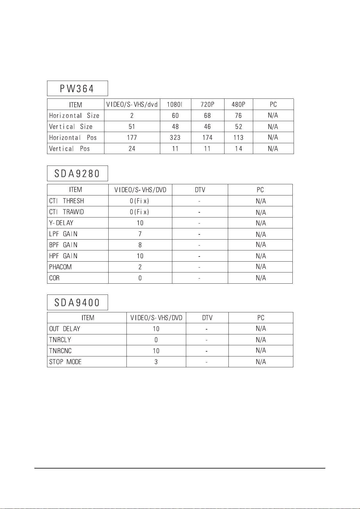
5-1-2 Initial DISPLAY State in times of SERVICE MODE Switch overs
PW364
INITIAL DISPLAY
SDA92 80 VPC3230 SDA9400
1, PW
364
2, SD
A9280
3, V
PC3230
4, SD
A9400
5, C
XA2101
6, A
D9884
7, O
SD POSITION
8, O
PTION
9, R
ESET
10, A
GING
H
orizonta lSize
V
er tical
Horizontal
Ve r t i ca l
Si
ze
Pos
Pos
CTIT
HRESH
CTIT
RAWID
Y- D
ELAY
L
PF GA IN
B
PF GAIN
H
PF GA IN
PH
ACOM
C
OR
B
RIGHT YUV
C
ONT YUV
I
FCOMP
ChromaB
and
L
uma LPF
H
PLL Speed
L
uma Delay
3230 Bri
ght
3230 C
ontr ast
HL
PF Y/ C
L
PF Chroma
HHPeak Fil
ter
PeakingG
ain
C
oaring off/ on
O
UT DELAY
TNRCLY
CLY
TNRCLC
CLY
ST
OP MODE
Page 12
Alignment and Adjustments
5-2 Samsung Electronics
5-1-3 Buttons Operations within SERVICE MODE
#Notice
The existing service data may be deleted after downloading a program. Be sure to make a backup copy of
your data before downloading and then restore the data after completing the download.
Menu
Channel UP/DOWN
Volume UP/DOWN
Entire menu display
Cursor move to select items
Enable to increase and decrease the data of the selected items
Limit Level
Sys tem
D-Color
R-DRIVE
-DRIVE
G
-DRIVE
B
R-Cutoff
G-Cutoff
-Cut off
B
ABL MODE
ABL TH
HSEPSEL
CONT RAST
BRI GHT
CR OFFSET
CB
OFFS ET1
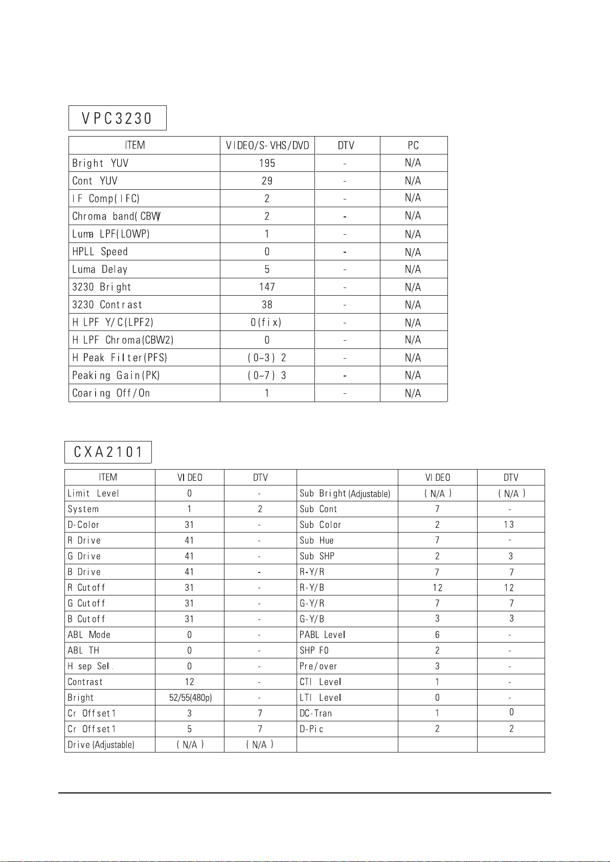
CXA2101 AD9884
DRIVE
SUB BRIGHT
SUB CONT
SUB COLOR
SUB HUE
SUB SHP
R-Y/R
R-Y/B
GG-Y/R
-Y/B
P
ABL LEVEL
SHP FO
PRE/OVER
CTI LEVEL
1
LTI LEVEL
DC - TRAN
D-PIC
RED
Gain
GREEN
BLUE
OFFSET
RED
GREEN
BLUE
GAIN DRIVE
OFFSET DIRVE
V CONTRAST
V BRIGHT
PHASE
CHANGE PUMP
Gain
Gain
OFFSET
OFFSET
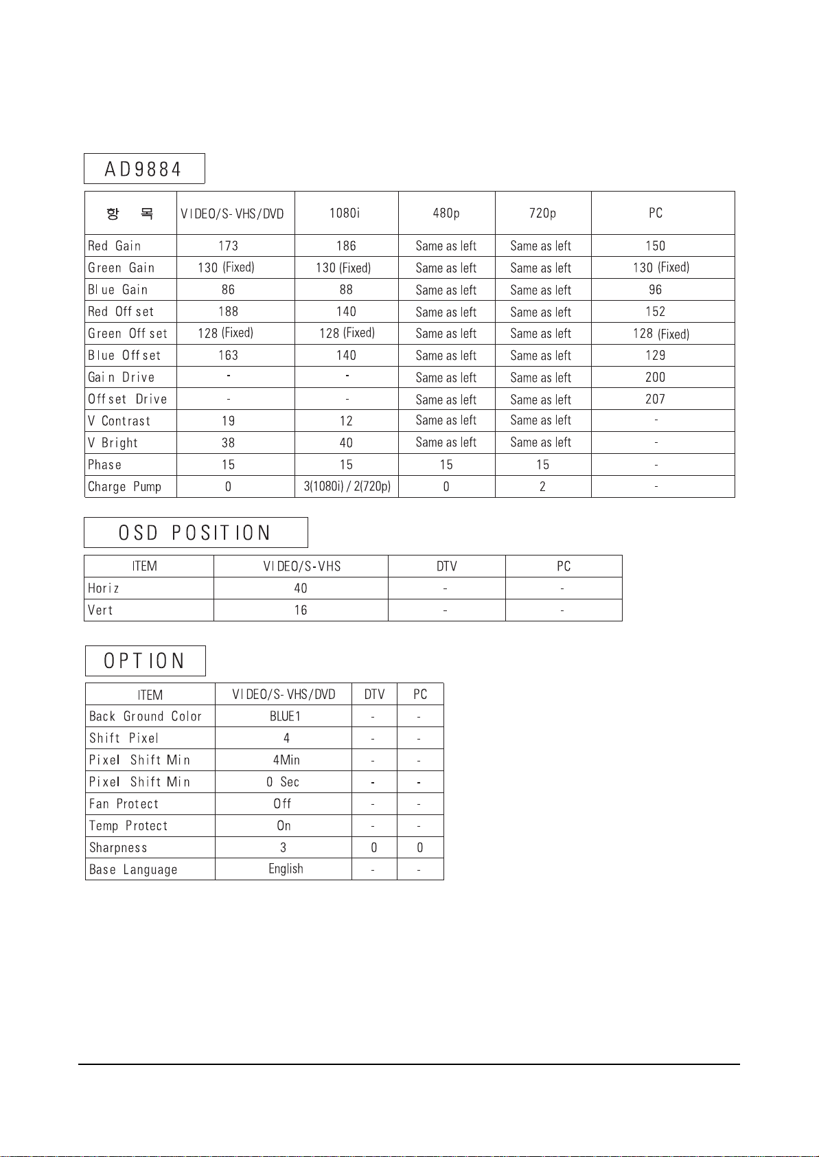
OSD
POSITION
HORIZ
VE RT
OP TION
1, BACK GR OUN D COLOR
SHIFT PIXEL
2,
PIXEL SHIFT
3,
PIXEL SHIFT
4,
FAN PROTECT
5,
TEMP
6,
7,
8, BASE LANGUAGE
PROTECT
SHARPNESS
MIN
SEC
Page 13
Alignment and Adjustments
Samsung Electronics 5-3
5-1-4 White Balance Adjust Method
1. Press MUTE-1-8-2-POWER to enter the factory mode.
2. Enter AD9884
3. Adjust LOW coordinates as R, B OFFSET and HIGH coordinates as R, B GAIN.(GREEN is fixed.)
4. In AD9884, adjust brightness with V CONTRAST / V BRIGHT for VIDEO / DTV, and adjust with
GAIN DRIVE / OFFSET DRIVE for PC.
1. VIDEO MODE (SPR-3100, input TOSHIBA PATTERN)
2. DTV MODE (SPR-3100, input TOSHIBA PATTERN)
A
dj ustme
nt
Adjustme
nt
Coor dinates
Coor dinates
Value
Deviation
A
dj ustme
nt
Adjustme
nt
Coor dinates
Coor dinates
Value
Deviation
H
-LIGHT
-LIGHT
x:286
y
:
274
Y
:
18.7(fL)
3
3
3
L
H-LIGHT
-LIGHT
L
x:278
y
:
272
Y
:0.53(f L)
(f L)
5
5
0. 1
x:288
y
:
277
Y: 16.1
Y:
3
3
3
x:280
y
:277
0.71
5
5
0. 1
- W/B Adjustment SPEC (Suwom Factory Toshiba PATTERN)
Page 14
Alignment and Adjustments
5-4 Samsung Electronics
2. PC MODE (VG828, input TOSHIBA PATTERN)
A
dj ustme
nt
Adjustme
nt
Coor dinates
Coor dinates
Value
Deviation
H-LIGHT
-LIGHT
L
x:287
y:288
Y: 21.3(fL)
Y:
x:287
y:294
2.17
3
3
3
5
5
0. 1
Page 15
Alignment and Adjustments
Samsung Electronics 5-5
5-1-5 SCALAR FACTORY DATA DEFAULT VALUES
Page 16
Alignment and Adjustments
5-6 Samsung Electronics
Page 17
Alignment and Adjustments
Samsung Electronics 5-7
Page 18
5-8 Samsung Electronics
Alignment and Adjustments
HPL6315
VGA
1
2
3
4
5
6
7
8
9
10
11
12
13
14
Video signal Dot X Line
640 X 350
640 X 400
VGA
WVGA
720 X 400
640 X 480
848 X 480
Ve rtical
Frequency (Hz)
70.086
85.080
85.080
70.087
85.039
59.940
72.809
75.000
85.008
60.000
72.000
75.000
85.000
56.250
Horizontal
Frequency (kHz)
31.469
37.861
37.861
31.469
37.927
31.469
37.861
37.500
43.269
29.838
35.156
36.072
37.650
42.925
Ve rtical
polarity
N
N
P
P
P
N
N
N
N
P
P
P
P
N/P
Horizontal
polarity
P
P
N
N
N
N
N
N
N
N
N
N
N
N/P
15
16
17
18
19
20
21
22
23
24
25
26
27
SVGA
XGA
WXGA
SXGA
800 X 600
1024 X 768
1152 X 864
1280 X 768
1280 X 1024
60.317
72.188
75.000
85.061
60.004
70.069
75.029
84.997
75.000
60
75
60.020
75.025
37.879
48.077
46.875
53.674
48.363
56.476
60.023
68.677
67.500
47.700
60.150
63.981
79.976
P
P
P
P
N
N
P
P
P
P
P
P
P
P
P
P
P
N
N
P
P
P
N
N
P
P
Page 19
Alignment and Adjustments
Samsung Electronics 5-9
5-2 Adjusting the Discharge Voltage Of the Main Unit While Replacing ASS'Y (Body Part)
Turning the variable resistor clockwise reduces voltage except VG, V9, and VR(6).
SMPS
OUT PUT Voltage(V)
1. V A
1. V FAN
3. SIGNAL
V5D
VFAN
VAMP
1. V SB
4. V 5A
11. V 12A
12. V 5D1
1. V 5D
3. V 5D
V5D1
VSET
VSCAN
VA
1. V A
2. V A
2. V A
1. V 5D
3. V G
5. V SCAN
7. V E
11. V S
12. V S
13. V S
VE
1. V 5D
3. V G
5. V E
7. V SCAN
10. V S
11. V S
12. V S
VS
VS 168
VE 183
VA 70
VSET 190
VSCAN 80
V5D 5
VFAN 12
VAMP 9
V5D1 5
V5A 5
V12A 12
VSB 5
V12A
V5A
VSB
1. V 5A
3. V 9A
4. V 12A
6. V AMP
7. V AMP
Page 20
Alignment and Adjustments
5-10 Samsung Electronics
Alignment and Adjustments
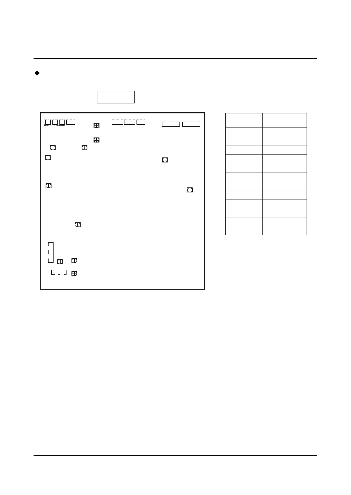
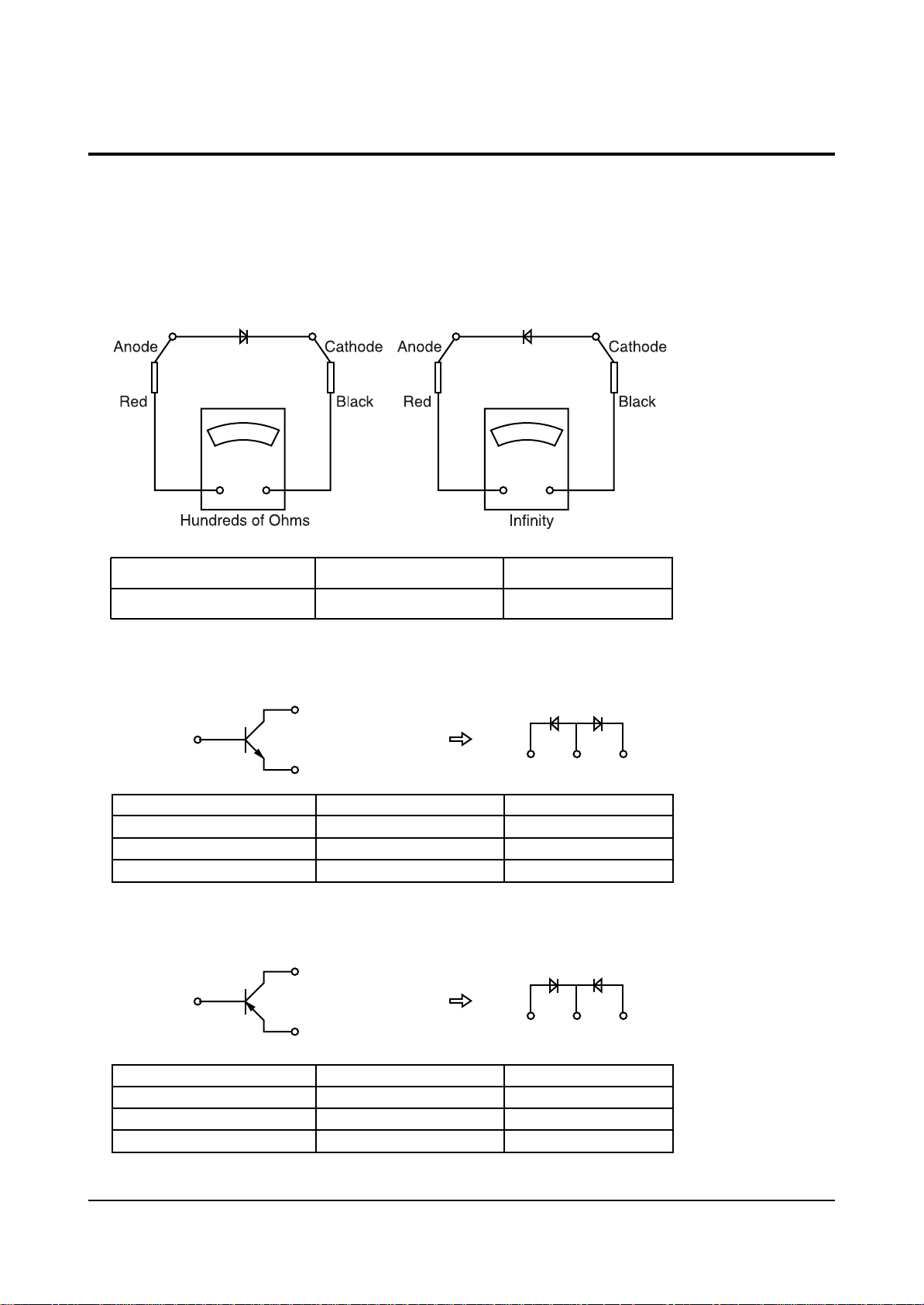
5-3 Fault Finding Using MULTI METER
Parts defects can be found for DIODE TRANSISTOR IC, using MULTI TEST including
Forward/Reverse direction Multi Test. Of course, in case resistance of several ohms and COIL are connected in parallel circuit, the lock out circuit parallel connected to part must be severed.
1.DIODE
2. TRANSISTOR
● For NPN(KSC815-Y, 2SC2068, 2SC2331-Y)
● For PNP(KSA539-Y)
Forward Direction
Hundreds of ohms
Reverse Direction
Infinity
Between Anode and Cathode
C (COLLECTOR)
E
B(BASE)
BC
C (COLLECTOR)
E
B(BASE)
BC
E (EMITTER)
E (EMITTER)
Forward Direction
Hundreds of ohms
Hundreds of ohms
Infinity
Reverse Direction
Infinity
Infinity
Infinity
Between B and E
Between B and C
Between E and C
Forward Direction
Hundreds of ohms
Hundreds of ohms
Infinity
Reverse Direction
Infinity
Infinity
Infinity
Between B and E
Between B and C
Between E and C
+- +-
Page 21

Alignment and Adjustments
Samsung Electronics 5-11
Alignment and Adjustments
3. IC (INTEGRATED CIRCUIT)
IC has built in DIODE against overvoltage in PIN. Generally, except for internal circuit defects, IC defects
can be found, by measuring the DIODE.
✍ Defects have SHORT(0 ohm) for both forward and reverse direction.
Hundreds of ohms
Forward Direction
Reverse Direction
Varying depending on IC but generally normal
Infinity in DIODE TEST MODE
Page 22

5-12 Samsung Electronics
MEMO
Page 23
Circuit Operation Description
Samsung Electronics 6-1
6. Circuit Description
6-1 Power supply
6-1-1 Outline(PDP SMPS)
Considering various related conditions, the switching regulator with good efficiency and allowing for its
small size and light weight was used as the power supply for PDP 50inch, VS requiring high power consumption used forward converter and 12VSAMP used the simple flyback converter and other high voltage
(VSCAN,VSET,VE)used DC/DC converter. To comply with the international harmonics standards and
improve the power factor, active PFC(Power Factor Correction) was used to rectify AC input into +400V
DC output, which in turns used as input to the switching regulator.
6-1-2 63"HD SMPS Specification
(1) Input
The PDP-PS-421S board should be designed so that the AC power supply within the 100VAC
(common) to 150VAC and the input frequency within 50/60Hz can be applied.
(2) Output
The PDP-PS-421S board converts the AC Voltages (+165Vs1, +75Va, +185Ve, +5Vd, +12Vcc, +6Vsp,
+9Vsp, +9Vcc, +12Vfan, +5Vd1, +5Va, +220Vset, +75Vscan, +18Vg) into the DC Voltages.
The usage and specification of each output is as shown in Table 1.
Table 1 shows the power supplies for PDP SMPS.
Table1. Specifications of Output Power Supplies for PDP SMPS
165Vs
75Va
185Ve
220Vset
75Vscan
5Vd
18Vg
5Vdl
5Va
9Vcc
12Vcc
6Vsp
12Vfan
5Vsb
165V ± 1%
75V ± 1%
185V ± 1%
220V ± 1%
75V ± 1%
5.2V ± 1%
18V ± 5%
5.2V ± 1%
5.2V ± 1%
9.2V ± 5%
12.2V ± 5%
6V ± 5%
11V ~ 14V
5.2V ± 1%
160V ~ 190V
60V ~ 85V
170V ~ 200V
200V ~ 250V
60V ~ 90V
4.5V ~ 5.5V
-
4.5V ~ 5.5V
-
-
-
3V ~ 24V
-
5.0V ~ 5.4V
0.2
0.2
0.01
0.01
0.01
0.3
0.07
0.2
0.1
0.07
0.07
0.25
0.1
0.1
2.0
2.0
0.1
→
→
→
→
→
→
→
→
2.5
→
1.0
0.2
0.2
0.01
0.01
0.01
0.3
0.07
0.2
0.1
0.07
0.07
0.25
0.1
0.1
Output
Voltage
(V)
Voltage
Setting
(Normal Load)
Output
Voltage
Variable Point
Output Current(A)
Min Non Max
Page 24

Circuit Operation Description
6-2 Samsung Electronics
(3) FUNCTION OF BOARD
1) Remote control
Using 120V/10A relay, the board makes remote control available.
2) Voltage
The board designed so that input voltage can be used within 100 VAC to 150VAC.
3) Improvement of power factor
The board is designed using PFC circuit so that PF (Power Factor) can be over 0.95, because
low PF can be a problem in high voltage power.
4) Protection
The OCP (Over Current Protection), the OVP (Over voltage Protection), and the Short Circuit
Protection functions are added against system malfunction.
(4) BLOCK DIAGRAM
This product can be defined as a power supply device (Input power: AC110/220V), consists of
Inrush Current Limit Circuit on Input and Power Factor Correction circuits, VS, VA, and VI Block,
providing the power (current) required for PDP Panel discharges and external circuits. PFC circuit
utilizes Discontinuous Current Mode ( DCM) that produces a high efficiency. And, an input EMI
filter circuit is equipped on the exterior.
1) PFC Block Boost Discontinuous Current Mode (DCM) PFC circuit is used for PFC (Power
Factor Correction), where a common PWM IC gives an easy control, a simple circuit onfiguration,
and a high efficiency. The circuit operates as described as following:RELAY is to be operated by
inputting initial Relay “ON” while the resistance for Inrush Current Limit charges a capacitor of
PFC Output Terminal. If the charged voltage of the capacitor goes over 340V, a comparator of
PFC circuit controller activates VA Block and Relay for Inrush Current Limit. Thereafter, PFC
circuit initiates a normal operation.
PFC circuit has output, voltage, current limit circuits for placing a restriction on switching current,
and protective (safeguard) circuits against output over-voltage. The over-voltage induces input
Terminal Relay to be “OFF” with the set shut down.
2) Vs Block supplies the sustain power closely related to PDP Panel and includes 165Vs and
185Ve employing a Full-bridge circuit as Topology. In order to insulate gate signal, Driver
at the secondary side based on properties of the pulse type of load. 185Ve power utilizes a
variable Regulator for sub-output of 165Vs power, which is supplied to the load being added to
165Vs power. 70kHz is applied for switching frequency that has the Sequence operated after
rising 5Vd power.
Table 2. Security function SPEC required for PDP SMPS
Division
+165Vs
+ 75Va
OCP Current
5 ~ 7A
3 ~ 4A
OVP Voltage
190 ~ 220V
85 ~ 100V
UVP Voltage
135 ~ 145V
50 ~ 65V
Short Circuit
OK
OK
Page 25
Circuit Operation Description
Samsung Electronics 6-3
Vs Switching Pulse(Pulse for power board operation only)
Va Switching Pulse(Pulse for Set ON)
Page 26
Circuit Operation Description
6-4 Samsung Electronics
3) Va Block Va Block consists of address voltage suppliers (75Va, 220Vset, and 75Vscan), VCCs
that supply a power to logic circuit, and 12V fan; the power of cooling Fan of 18Vg. PDP Set
that provides Gate voltages of drive circuit. It utilizes a Forward circuit mode as TOpology.
75Vscan uses 75Va power to construct not only stable but, if needed, also variable DC/DC
Converter while 220Vset, also variable if wanted, is applied by adding 165Vs power to the power
generated from Buck Converter with 75Va power. 5Vd and 12Vsp power can be generated by
Buck Converter with the power gained through Coupling in Transformer, and 18Vg by Linear
Regulator. The switching frequency is 70kHz.
Va Switching Pulse(Pulse for Set ON)
4) Block VI Block consists of voltage suppliers for image circuits (5Va, 9Vcc, 12Vcc, and 5Vd1),
and a Flyback circuit mode is applied as Topology. Feedback for voltage stability is designed for
5Vd1, 5Va, 9Vcc, 12Vcc, and 5Vd1 powers anr generated by using each Linear Regulator for the
power gained through Coupling in Transformer. The switching frequency is 100kHz.
Page 27
Circuit Operation Description
Samsung Electronics 6-5
VI Switching Pulse(Pulse for power board operation only)
VI Switching Pulse(Pulse for Set ON)
Page 28
Circuit Operation Description
6-6 Samsung Electronics
6-1-3 Pin Assignment
Image Board
NO OUT PUT
1
2
3
4
5
6
7
8
9
10
11
12
13
+5V
GND(D)
GND(D)
+5V
RELAY
THDET
FAN
GND
GND
N.C
+12V
+5V
N.C
LOC
VSB
V5(D)
V12
V5(D)
SX(X Driver)
OUT PUT
NO
1 +5V
2
3
4
5
6
7
8
9
10
11
12
13
GND
+18V
GND
70V
GND
230V
N.C
GND
GND
165V
165V
165V
LOC
V5(D)
VG
VSCAN
VS
VS
VS
SY (Y Drive)
NO
OUT PUT
1 +5V(D)
2
3
4
5
6
7
8
9
10
11
12
GND(D)
+18V
GND
200V
GND
70V
GND
GND
165V
165V
165V
LOC
V5(D)
VG
VE
VSCAN
VS
VS
VS
Speaker
NO OUT PUT
1
2
3
4 +12V V12
5 GND
6 VSAMP
7 VSAMP
8
9
+5V
GND
+9V
+6V
+6V
GND
GND
LOC LOC
V9
Buffer(2EA) SL(Logic)
NO OUT PUT
1
2
3
4
NO OUTPUT
1 +12V VFAN
2 GND
+70V
+70V
GND
GND
Fan(3EA)
VA
VA
LOC
NO
1
2
3
4
OUT PUT
+70V
+70V
GND
GND
LOC
Page 29
Circuit Operation Description
Samsung Electronics 6-7
6-1-4 SMPS Block diagram
AC
INPUT
PFC
VS
BLOCK
VA
BLOCK
Reg.
DC/DC
DC/DC
Reg.
BUCK
BUCK
GND
GND
GND
GND
GND
GND
GND
GND
GND
185VE
165VS
220VET
75VSCAN
75VA
18VG
5VD
6VSP
12VFAN
AC
INPUT
VI
BLICK
Reg.
Reg.
Reg.
GND
GND
GND
GND
GND
5VD1
5VA
9VCC
12VCC
5VSB
Page 30

Circuit Operation Description
6-8 Samsung Electronics
6-2 Driver circuit
6-2-1 Driver circuit overview
6-2-1(A) WHAT IS THE DRIVER CIRCUIT
It is a circuit generating an appropriate pulse (High voltage pulse) and then driving the panel to implement
images in the external terminals (X electrode group, Y electrode group and address electrode), and this high
voltage switching pulse is generated by a combination of MOSFETs.
6-2-1(B) PANEL DRIVING PRINCIPLES AND TYPES OF DISCHARGE BY DRIVE PULSE
In PDP, images are implemented by impressing voltage on the X electrode, Y electrode and address
electrode, components of each pixel on the panel, under appropriate conditions. Currently, ADS (Address &
Display Separate: Driving is made by separating address and sustaining sections) is most widely used to
generate the drive pulse. Discharges conducted within PDP pixels using this method can largely be
classified into 3 types, as follows:
Address discharge: This functions to generate wall voltage within pixels to be lighted by addressing
information to them (i.e., impressing data voltage)
Sustaining discharge: This means a display section where only pixels with wall voltage by the
address discharge display self-sustaining discharge by the support of such wall voltage. (Optic outputs realizing images are generated.)
Ramp reset discharge: To have address discharge occur selectively in pixels, all pixels in the panel
must have the same conditions (i.e., the same state of wall and space electric discharges). The ramp
reset discharge section, therefore, is important to secure the drive margin, and methods most widely
used to date include wall voltage controlling by ramp pulse.
Page 31

Circuit Operation Description
Samsung Electronics 6-9
6-2-1(C) Discharge of Drive
Sustaining discharge
1(C). Kinds and detailed descriptions of driving discharge
Sustaining discharge means a self-sustaining discharge generated by the total of the sustaining pulse
voltage (usually, 160~180V) alternately given to X and Y electrodes during the sustaining period and
the wall voltage which varies depending upon pixels' previous discharge status. It is operated by the
memory function (through this, the current status is defined by previous operation conditions) AC
PDP basically possesses. That is, when there is existing wall voltage in pixels (in other words, when
pixels remain ON), the total of wall voltage and a sustaining voltage to be impressed subsequently
impresses a voltage equal to or above the discharge start voltage, thereby generating discharge again,
but when there is no existing wall voltage in pixels (in other words, when pixels remain OFF), the
sustaining voltage only does not reach the discharge start voltage, thus causing no discharge. The
sustaining discharge is a section generating actual optic outputs used in displaying images.
Address discharge
This means a discharge type generated by the difference between positive voltage of the address
electrode (usually, 60~70V) and GND of the Y electrode. The address discharge serves to generate
wall voltage in pixels where images are to be displayed (that is, discharge is to be generated) prior to
the sustaining discharge section. Namely, pixels with wall voltage by the address discharge will generate sustaining discharge by the following sustaining pulses.
Weak erasing discharge
The purpose of resetting discharge is to make even wall voltage in all pixels on the panel.
Wall voltage which may vary depending upon the previous sustaining discharge status must be
made even. That is, wall voltage generated by the sustaining discharge must surely be removed, by
making discharges and then supplying ions or electrons. Wall voltage can be removed by making
discharges and then setting a limitation on time for opposite polarity charging of the wall voltage or
generating weak discharge (Low voltage erasing) to supply an appropriate quantity of ions or
electrons and keep polarities from being charged oppositely. The weak discharge (Low voltage erasing) methods which have been known to date can largely be into two types:
1) the log pulse adopted by most companies including F Company, and
2) the ramp pulse adopted by Matsushita.
In both two methods, impression is made with a slow rising slope of the erasing pulse. Because the
total of the existing wall voltage and a voltage on the rising pulse must be at least the drive start
voltage to generate discharges, external impressed voltage is adjusted based on the difference in wall
voltage between pixels.
And, weak discharge is generated because of a small impressed voltage.
Page 32

Circuit Operation Description
6-10 Samsung Electronics
6-2-2 Driver Circuit Block Diagram
(1) Y
(2) X
Fig. Driver Y-Bd
Fig. Driver Y-Bd
LOGIC SIGNAL INPUT
LOGIC SIGNAL BUFFER
FET GA TE DR IV ER
Reco very
Switching
Main
Switching
Reco very circuit
(Recovery Cap)
POWER SUPPLY INPUT
5V
17V
170V
Vs et
Switching
220V
75V
Vs ca n
Switching
LOGIC SIGNAL INPUT
LOGIC SIGNAL BUFFER
FET GATE DRIVER
Reco very
Switching
Reco very circuit
(Recovery Cap)
POWER SUPPLY INPUT
5V
17V
Main
Switching
200V
170V
Ve
Switching
Page 33

(3) Key Requirements of the Driver Circuit Operations
1) Power Supply
- Power is supplied from the power board. The minimum value may differ from the following.
2) Logic Signals
- Logic signals are supplied from the logic board.
- Gate signals of each FET
(4) Diagram and Functional Description of the Driver Circuit
- Functional Description of Each Board
Circuit Operation Description
Samsung Electronics 6-11
X- Bu ffe r
(Upper Part)
X Driver Board
-Sustain waveforms
mp waveforms
a
(Energy Recove ry)
-Rising R
Y- Sub X - Sub
X- Bu ffe r
(Lower Part)
(6 block)
X electrode port
(Energy Recovery)
X Driver Board
- Sustain waveforms
- RisingRamp waveforms
-Vebias
-Vebias
COB
waveforms
(Energy Recover y)
Y Driver Board
- Sustain waveforms
- Rising Ramp waveforms
- Falling Ramp waveforms
- Vscan waveforms
(Energy Recovery)
Y Driver Board
- Sustain waveforms
- RisingRamp waveforms
- Fa lling Ramp
- Vscan waveforms
(6 block)
Y- Buffer
(Upper Part)
Y- Buffer
(Lower Part)
Page 34

1) X Board I, II
X Board I and II are connected to the X port on the panel to:
- Produce sustain voltage waveforms (including ERC)
- Produce X rising ramp waveforms
- Sustain Ve bias during the Scan.
2) Y Board I, II
Y Board I and II are connected to the Y port on the panel to:
- Produce sustain voltage waveforms (including ERC)
- Produce Y rising ramp waveforms
- Sustain V scan bias.
3) X Buffer Board (Upper and Lower)
The X buffer board applies Sustain waveforms to the X port. It consists of an upper and
a lower board.
4) Y Buffer Board (Upper and Lower)
The Y buffer board applies Scan waveforms to the Y port. It consists of an upper and a
lower board. Each board is installed with 6 Scan driver ICs (STMicroelectronics
STV7616: 64 or outputs).
5) X Sub Board
The X sub board distributes and applies logic data to the X board I and II.
6) Y Sub Board
The Y sub board distributes and applies logic data to the Y board I and II.
7) COB
The COB applies Va waveforms to the Address electrodes during the Address stage to
produce Address discharges by using the difference between the injection waveforms
and the voltage applied to the Y electrode. ACOB is installed with 4 data drive ICs
(STMicroelectronics STV7610A: 96 outputs). A total 22 COBs are required.
Circuit Operation Description
6-12 Samsung Electronics
Page 35

Circuit Operation Description
Samsung Electronics 6-13
6-2-3 Driving Waveform Specs
6-2-3(A) Driving Waveform Diagram
Vs
Vscan
Xsustain
pulse
Vs
Ysustain
pulse
Y s can
pulse
Ve
Y falling
Ramp
Va
Addres s
pulse
Vs 160~170V Ve 190V~200V
Vs e t 210~225V Va 70~75V
Vs c a n 70~75V
Vs e t
Ve
Y r is ing
Ramp
X r is ing
Ramp
Y
X
RESET SCAN SUSTAI N
X Co mmon & Sus t a i n El e ct r ode
Ad d r e s s
A1 , 2 . . . . . Address( =Dat a) Elect rode
Y1 , 2 . . . . Scan &Sustain Electrode
Page 36

Circuit Operation Description
6-14 Samsung Electronics
6-2-3(B) Functional Description of Each Waveform
(1) X Rising Ramp Waveform
The last Y electrode Sustain waveform is applied from the sub field before the XZ Rising Ramp
waveforms begin to be applied. The last waveform triggers the Sustain Discharge.
Then, a positive wall charge occurs on the X electrodes and a negative wall chanrge on the Y
electrodes.
The X rising ramp eliminates the wall charge produced by the aforementioned Sustain Discharge
waveform by triggering a low discharge.
(2) Y Rising Ramp Waveform
During the Y Rising Ramp stage, an external voltage of 390-400V is applied to the Y electrodes to
adjust each Gap Voltage to the same initial voltage level before starting a low discharge. As the low
discharge is sustained, a negative wall charge continues on the Y electrodes and a positive wall
charge on the X and Address electrodes across the panel.
(3) Y Falling Ramp Waveform
During the Y Falling Ramp stage, most of the negative wall charges on the Y electrodes,
with approximately 200V X bias, are used to eliminate the positive wall charges on the
X electrodes. Most of the positive wall charges on the (OV) rising ramp section of the
Address electrodes are sustained to form wall charges in preparation for an address discharge.
(4) Y Scan Wavdform
The Y Scan waveform is also calle an injection waveform. It selects Y electrodes one
line at a time. Vscan is referred to as Scan bias voltage. About 70 Volts (V scan)are
applied to the applicable electrode limes with Vscan, and 0 Vots (GND) to the rest.
When Ramp waveforms are applied, however, a negative wall charge occurs on the Y
electrodes, and a positive wall charge on the Address electrodes. Because the voltage
level exceeds the initial discharge level in those cells affected by address waveforms
(70~75V), an address discharge occurs. The PDP Address takes a long time because it
applies injection and data waveforms line by line.
Page 37

Circuit Operation Description
Samsung Electronics 6-15
6-2-3(C) Principles of Fets Operation and High Voltage Switching
1) With signal impressed on the gate(Positive voltage) ,
FET gets short-circuited (a conducting wire of zero
(0) resistance); and
2) With no signal impressed on the gate (GND), FET
gets open-circuited (a non-conducting wire of ∞
resistance).
1) With no signal impressed on G1, FET1 gets open-circuited, and with signal impressed on G2, FET2
gets short-circuited, thereby causing GND to be outputted to output terminals.
2) With signal impressed on G1, FET1 gets short-circuited, and with no signal impressed on G2, FET2
gets open-circuited, thereby causing 180V to be outputted to output terminals.
Page 38

Circuit Operation Description
6-16 Samsung Electronics
6-2-3(D) Driver Circuit Composition Diagram
C_Xerc
VsVe
D_Xs
C_Xsink
Dscan
Xr
Xs
D_Xsink
Xrr
D_Ysink
Ramp
D_Xr
D_YVsC
LX
Cp
3
1
2
Xg
D_Xf
Xf
D_YGC
3 2
1
0 0
0
VscanVset
Vs
Ysc
Rset
Yrr
Ys
Ysp
C_Ysink
Ramp
Dset
D_YVsC
Yr
Yp
Cset
LY
D_Yr
+5V
Yfr
Yg
D_Yf
C_Yerc D_YGC
floating 5V
D_fVdd
Ramp
Yf
C_fVdd
0 0 00
Page 39

Circuit Operation Description
Samsung Electronics 6-17
6-2-3(E) Driver Board Connector Layout
(1) X I
CN4004
- Power
CN4406
- Panel
CN4005
- Signal
CN4009
CN4008
CN4007
CN4006
CN4402
CN4401
CN4404
CN4403
CN44 05
CN4407
- Panel
CN4408
- Panel
Page 40

Circuit Operation Description
6-18 Samsung Electronics
(2) X II
CN4004
- Power
CN4009
CN4008
CN4505
CN45 01
CN45 03
CN4506
- Panel
CN4005
- Signal
CN4007
CN4006
CN45 02
CN45 04
CN4508
- Panel
CN4507
- Panel
Page 41

Circuit Operation Description
Samsung Electronics 6-19
(3) Y I
CN5401
- Panel
CN5402
- Panel
CN5404
CN5406
CN5405
CN5407
CN5409
CN5008
- Power
CN5007
CN5001
CN5006
CN5005
CN5003
CN5403
- Panel
CN5408
CN5004
CN5002
- Signal
Page 42

Circuit Operation Description
6-20 Samsung Electronics
(4) Y II
CN5503
- Panel
CN5502
- Panel
CN5508
CN5509
CN5507
CN5505
CN5506
CN5007
CN5001
CN5006
CN5005
CN5008
-
Power
CN5501
- Panel
CN5003
CN5504
CN5004
CN5002
- Signal
Page 43

Circuit Operation Description
Samsung Electronics 6-21
Single scan mode PDP action : Rest section, X : 0 -> Ve, Y : 0
C_Xerc
VsVe
VscanVset
D_Xs
C_Xsink
Dscan
D_Xsink
D_Ysink
Ysc
Xr
Xs
Xrr
Ramp
C_Ysink
Ysp
D_Xr
D_YVsC
LX
Cp
1
D_Xf
Xf
D_YGC
0 0
0
Xg
155V
Vs :155V
2
3
3 2
1
floating 5V
Vs
Rset
Ys
Yrr
Ramp
Dset
Yr
Yp
Cset
LY
D_YVsC
D_Yr
+5V
Yfr
Yg
D_Yf
C_Yerc D_YGC
D_fVdd
Ramp
Yf
C_fVdd
0 0 00
V set + V s:355V
Y rise
155V
155V
Va :78V
Vscan :65V 65V
Ve :184V
Yfall
RESET SCAN SUSTA IN
Vs :155V
184V
Y
X rise
X
Address
Page 44

Circuit Operation Description
6-22 Samsung Electronics
Single scan mode PDP action : Rest section, X : 0 , Y : Vs -> Vs + Vset
C_Xerc
VsVe
VscanVset
C_Xsink
Dscan
D_Xs
D_Xsink
Ysc
Xr
Xs
Xrr
Ramp
D_Ysink
C_Ysink
Ysp
D_Xr
D_YVsC
LX
Cp
1
D_Xf
Xf
D_YGC
0 0
0
Xg
155V
Vs :155V
2
3
3 2
1
floating 5V
Vs
Rset
Ys
Yrr
Ramp
Dset
Yr
Yp
Cset
LY
D_YVsC
D_Yr
+5V
Yfr
Yg
D_Yf
C_Yerc D_YGC
D_fVdd
Ramp
Yf
C_fVdd
0 0 00
V set + V s:355V
Y rise
155V
155V
Va :78V
Vscan :65V 65V
Ve :184V
Yfall
RESET SCAN SUSTA IN
Vs :155V
184V
Y
X rise
X
Address
Page 45

Circuit Operation Description
Samsung Electronics 6-23
Single scan mode PDP action : Rest section, X : Vs, Y : Vs
C_Xerc
VsVe
VscanVset
D_Xs
C_Xsink
Dscan
D_Xsink
D_Ysink
Ysc
Xr
Xs
Xrr
Ramp
Ysp
C_Ysink
D_Xr
D_YVsC
LX
Cp
3
1
D_Xf
D_YGC
Xg
2
1
floating 5V
Xf
0 0
0
155V
Vs : 155V
3 2
Vs
Rset
Ys
Yrr
Ramp
Dset
Yr
Yp
Cset
LY
D_YVsC
D_Yr
+5V
Yfr
Yg
D_Yf
C_Yerc D_YGC
D_fVdd
Ramp
Yf
C_fVdd
0 0 00
Va :78V
Vscan : 65V 65V
Ve :184V
Y fall
155V
V set + V s:355V
Y rise
155V
Y
184V
Vs : 155V
X rise
X
Ad dress
RESET SCAN SUSTA IN
Page 46

Circuit Operation Description
6-24 Samsung Electronics
Single scan mode PDP action : Rest section, X : Ve, Y : Vs
C_Xerc
VsVe
VscanVset
C_Xsink
Dscan
D_Xs
D_Xsink
Ysc
Xr
Xs
Xrr
Ramp
D_Ysink
C_Ysink
Ysp
D_Xr
D_YVsC
LX
Cp
1
D_Xf
Xf
D_YGC
0 0
0
Xg
155V
Vs :155V
2
3
3 2
1
floating 5V
Vs
Rset
Ys
Yrr
Ramp
Dset
Yr
Yp
Cset
LY
D_YVsC
D_Yr
+5V
Yfr
Yg
D_Yf
C_Yerc D_YGC
D_fVdd
Ramp
Yf
C_fVdd
0 0 00
V set + V s:355V
Y rise
155V
155V
Va :78V
Vscan :65V 65V
Ve :184V
Yfall
RESET SCAN SUSTA IN
Vs :155V
184V
Y
X rise
X
Address
Page 47

Circuit Operation Description
Samsung Electronics 6-25
Single scan mode PDP action : Rest section, X : Ve, Y : Vs -> 0
C_Xerc
VsVe
VscanVset
D_Xs
C_Xsink
Dscan
D_Xsink
D_Ysink
Ysc
Xr
Xs
Xrr
Ramp
C_Ysink
Ysp
D_Xr
D_YVsC
LX
Cp
1
D_Xf
Xf
D_YGC
0 0
0
Xg
155V
Vs :155V
2
3
3 2
1
floating 5V
Vs
Rset
Ys
Yrr
Ramp
Dset
Yr
Yp
Cset
LY
D_YVsC
D_Yr
+5V
Yfr
Yg
D_Yf
C_Yerc D_YGC
D_fVdd
Ramp
Yf
C_fVdd
0 0 00
V set + V s:355V
Y rise
155V
155V
Va :78V
Vscan :65V 65V
Ve :184V
Yfall
RESET SCAN SUSTA IN
Vs :155V
184V
Y
X rise
X
Address
Page 48

Circuit Operation Description
6-26 Samsung Electronics
Single scan mode PDP action : Rest section, X : Ve, Y : Vscan, idle scan-line
C_Xerc
VsVe
VscanVset
C_Xsink
Dscan
D_Xs
D_Xsink
Ysc
Xr
Xs
Xrr
Ramp
D_Ysink
C_Ysink
Ysp
D_Xr
D_YVsC
LX
Cp
1
D_Xf
Xf
D_YGC
0 0
0
Xg
155V
Vs :155V
2
3
3 2
1
floating 5V
Vs
Rset
Ys
Yrr
Ramp
Dset
Yr
Yp
Cset
LY
D_YVsC
D_Yr
+5V
Yfr
Ramp
Yg
D_Yf
C_Yerc D_YGC
D_fVdd
Yf
C_fVdd
0 0 00
V set + V s:355V
Y rise
155V
155V
Va :78V
Vscan :65V 65V
Ve :184V
Yfall
RESET SCAN SUSTA IN
Vs :155V
184V
Y
X rise
X
Address
Page 49

Circuit Operation Description
Samsung Electronics 6-27
Single scan mode PDP action : Rest section, X : Ve, Y : Vscan, address scan-line
C_Xerc
VsVe
VscanVset
C_Xsink
Dscan
D_Xs
D_Xsink
Ysc
Xr
Xs
Xrr
Ramp
D_Ysink
C_Ysink
Ysp
D_Xr
D_YVsC
LX
Cp
1
D_Xf
Xf
D_YGC
0 0
0
Xg
155V
Vs :155V
2
3
3 2
1
floating 5V
Vs
Rset
Ys
Yrr
Ramp
Dset
Yr
Yp
Cset
LY
D_YVsC
D_Yr
+5V
Yfr
Yg
D_Yf
C_Yerc D_YGC
D_fVdd
Ramp
Yf
C_fVdd
0 0 00
V set + V s:355V
Y rise
155V
155V
Va :78V
Vscan :65V 65V
Ve :184V
Yfall
RESET SCAN SUSTA IN
Vs :155V
184V
Y
X rise
X
Address
Page 50

Circuit Operation Description
6-28 Samsung Electronics
Single scan mode PDP action : Rest section, X : Ve, Y : Vscan, idle scan-line
C_Xerc
VsVe
VscanVset
C_Xsink
Dscan
D_Xs
D_Xsink
Ysc
Xr
Xs
Xrr
Ramp
D_Ysink
C_Ysink
Ysp
D_Xr
D_YVsC
LX
Cp
1
D_Xf
Xf
D_YGC
0 0
0
Xg
155V
Vs :155V
2
3
3 2
1
floating 5V
Vs
Rset
Ys
Yrr
Ramp
Dset
Yr
Yp
Cset
LY
D_YVsC
D_Yr
+5V
Yfr
Ramp
Yg
D_Yf
C_Yerc D_YGC
D_fVdd
Yf
C_fVdd
0 0 00
V set + V s:355V
Y rise
155V
155V
Va :78V
Vscan :65V 65V
Ve :184V
Yfall
RESET SCAN SUSTA IN
Vs :155V
184V
Y
X rise
X
Address
Page 51

Circuit Operation Description
Samsung Electronics 6-29
Single scan mode PDP action : Rest section, X : 0, Y : 0, GND mode
C_Xerc
D_XrXfD_Xf
Xr
VsVe
VscanVset
C_Xsink
Dscan
D_Xs
D_Xsink
Ysc
Rset
Xs
Xrr
Ramp
D_Ysink
C_Ysink
Yrr
Ramp
Dset
Ysp
D_YVsC
1
Yp
Cset
Cp
LX
3
2
+5V
Yfr
D_YGC
Xg
1
D_fVdd
3 2
floating 5V
C_fVdd
0 0
0
155V
Vs :155V
Va :78V
Vscan :65V 65V
Ve :184V
Yfall
Vs
Ys
Yr
LY
D_YVsC
D_Yr
Ramp
Yg
D_Yf
Yf
0 0 00
V set + V s:355V
Y rise
155V
155V
RESET SCAN SUSTA IN
Vs :155V
184V
Y
X rise
X
Address
C_Yerc D_YGC
Page 52

Circuit Operation Description
6-30 Samsung Electronics
Single scan mode PDP action : Rest section, X : 0, Y : 0 -> Vs, charging mode
C_Xerc
VsVe
VscanVset
C_Xsink
Dscan
D_Xs
D_Xsink
Ysc
Xr
Xs
Xrr
Ramp
D_Ysink
C_Ysink
Ysp
D_Xr
D_YVsC
LX
Cp
1
D_Xf
Xf
D_YGC
0 0
0
Xg
155V
Vs :155V
2
3
3 2
1
floating 5V
Vs
Rset
Ys
Yrr
Ramp
Dset
Yr
Yp
Cset
LY
D_YVsC
D_Yr
+5V
Yfr
Ramp
Yg
D_Yf
C_Yerc D_YGC
D_fVdd
Yf
C_fVdd
0 0 00
V set + V s:355V
Y rise
155V
155V
Va :78V
Vscan :65V 65V
Ve :184V
Yfall
RESET SCAN SUSTA IN
Vs :155V
184V
Y
X rise
X
Address
Page 53

Circuit Operation Description
Samsung Electronics 6-31
Single scan mode PDP action : Rest section, X : 0, Y : Vs, Gas discharging mode
C_Xerc
VsVe
VscanVset
D_Xs
C_Xsink
Dscan
D_Xsink
D_Ysink
Ysc
Xr
Xs
Xrr
Ramp
C_Ysink
Ysp
D_Xr
D_YVsC
LX
Cp
1
D_Xf
Xf
D_YGC
0 0
0
Xg
155V
Vs :155V
2
3
3 2
1
floating 5V
Vs
Rset
Ys
Yrr
Ramp
Dset
Yr
Yp
Cset
LY
D_YVsC
D_Yr
+5V
Yfr
Yg
D_Yf
C_Yerc D_YGC
D_fVdd
Ramp
Yf
C_fVdd
0 0 00
V set + V s:355V
Y rise
155V
155V
Va :78V
Vscan :65V 65V
Ve :184V
Yfall
RESET SCAN SUSTA IN
Vs :155V
184V
Y
X rise
X
Address
Page 54

Circuit Operation Description
6-32 Samsung Electronics
Single scan mode PDP action : Rest section, X : 0, Y : Vs -> 0, discharge mode
C_Xerc
VsVe
VscanVset
D_Xs
C_Xsink
Dscan
D_Xsink
D_Ysink
Ysc
Xr
Xs
Xrr
Ramp
C_Ysink
Ysp
D_Xr
D_YVsC
LX
Cp
1
D_Xf
Xf
D_YGC
0 0
0
Xg
155V
Vs :155V
2
3
3 2
1
floating 5V
Vs
Rset
Ys
Yrr
Ramp
Dset
Yr
Yp
Cset
LY
D_YVsC
D_Yr
+5V
Yfr
Yg
D_Yf
C_Yerc D_YGC
D_fVdd
Ramp
Yf
C_fVdd
0 0 00
V set + V s:355V
Y rise
155V
155V
Va :78V
Vscan :65V 65V
Ve :184V
Yfall
RESET SCAN SUSTA IN
Vs :155V
184V
Y
X rise
X
Address
Page 55

Circuit Operation Description
Samsung Electronics 6-33
6-3 Logic part
6-3-1 Description of Logic Board
The logic board consists of a logic main board and a buffer board. The logic main board is made up
of a data signal processor that processes video signals, and a XY signal generator that runs the XY
drivers. The buffer boar stores address driver output sigals and sends them to the address driver IC
(COF module).
6-3-2 Name and Description of Major COmponents of the Logic Board
Logic Board Function Remarks
(Lo gic M a in)
(Bu ffe r Bo a rd )
E, F, G Buffer oard
H, I, J Buffer board
- Processes video signals. (W/L, Error diffusion, APC)
- Outputs address driver control signals and data
signals to the buffer board.
- Outputs XY driver board control signals
Sends data signals and control signalss to the upper
COF.
Sends data signals and control signals to the lower
COP.
*
!
@
#
(
$
)
^&
%
Page 56

Circuit Operation Description
6-34 Samsung Electronics
Description
NO
An input connector that receives LVDS encoded RGB, H, V, DATAEN, and
DCLK signals from the video board.
Indicates if the logic board properly receives Sync and
clock signal.
A connector to the Key Scan board that check and adjust
24C16 data.
An EEPROM for saving the gamma table, the APC table, the drive signal
timing and other options, etc.
A connector that outputs Y driver board control signals.
A connector that outputs X driver board control signals.
A connector that outputs address data and control signals to the
E,F and G buffer board.
A connector that outputs address data and control signals to the
H,I and J buffer board.
A fuse connected to the power source (5V) of the logic board.
A connector that supplies power (5V) to the logic board.
LVDS Connector
Operation LED
Key Scan Connector
256K
Y Connector
X Connector
Address Buffer
Connector (E,F,G)
Address Buffer
Connector (H,I,J)
Power Fuse
Power Connector
NAME
6-3-3 Waveform in Normal Operation
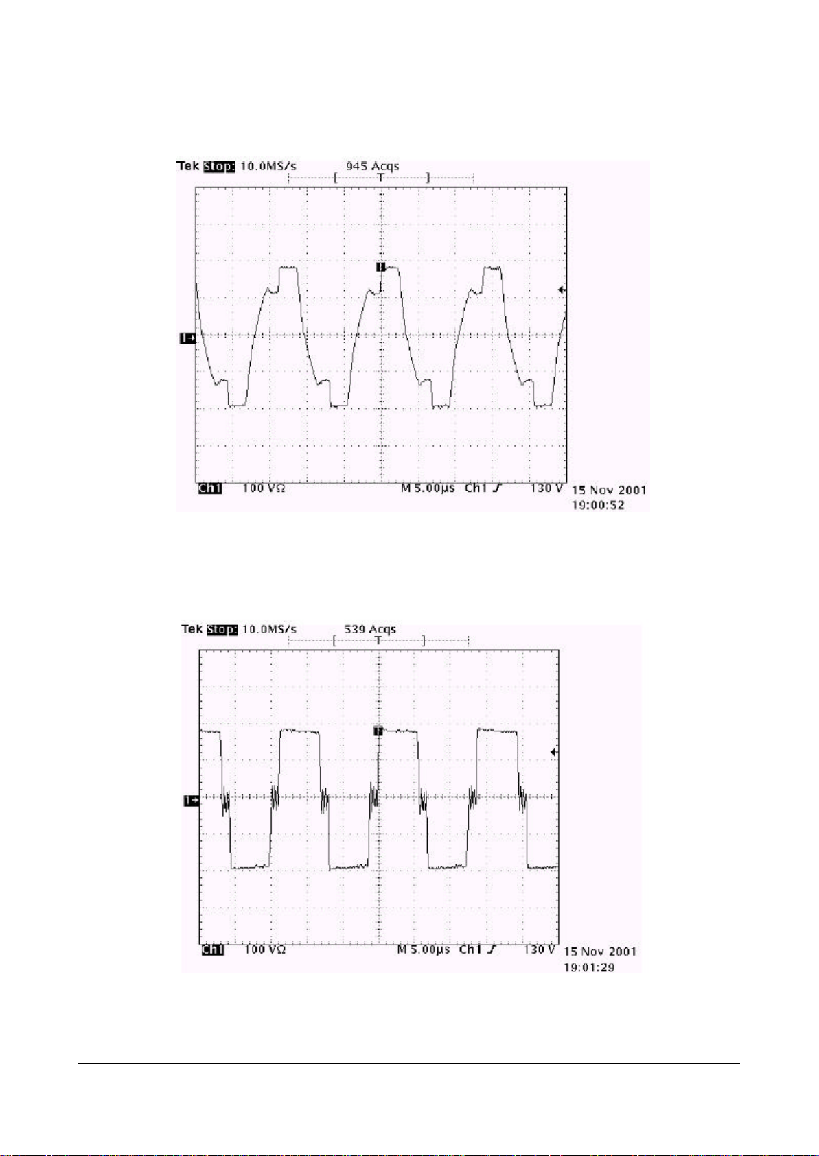
If the PDP unit and the logic board are operationg properly, the LED LD2010 in Figure 1 will blink
at about a 1 second interval.
If the unit is out of order, check the status of the Operation LED through eye-inspection first.
If the behavior of the Operation LED is different from that of normal operation, you have to replace
the board. To trouble-shoot the board, complete the logic board test procedures attached in the
Appendix.
Page 57

Circuit Operation Description
Samsung Electronics 6-35
6-3-3(A) Layout and Apperance of the Board
(1) Input
Fig. 1 Layout of the Logic Mainboard
LD2010
LD2002
LD2001
KEYSCAN
LG2000
F3
F2
256K
CN2001
256K
F1
TP1
U2002
GND
U2003
LG2003LG2002LG2001
U2005
U2006
U2007
U2008
CN2002
U2009
U2004
U2 010
LY2000
CN2003
LE2001 LE2002 LE2003
Page 58

(2) Appearance of and Markings on the Connector
Basically, it is depicted exactly the same as the real one on the PCB.
6-3-3(B) DIP Switch setting that selects the internal or external clock (CN2001)
(1) External Mode Selection
Circuit Operation Description
6-36 Samsung Electronics
☞ When External Mode is selected;
! Enter PAGE 00.
@ Set Register 2E’s address to 01.
# Adjust the Dip Switch as shown above.
(UP : PIN_NUMBER 6,5,3,2,1 / DOWN : PIN_NUMBER 4)
(2) Internal Mode NTSC Pattern Selection
☞ When Internal Mode Pattern is selected;
! Enter PAGE 00.
@ Set Register 2E’s address to 01.
# Adjust the Dip Switch as shown above.
(UP : PIN_NUMBER 6,5,4,3,2 / DOWN : PIN_NUMBER 1)
MODE PAGE
NTSC 00 2E 01
REGISTER
ADDRESS
EXTERNAL
MODE VALUE
MODE PAGE
REGISTER
ADDRESS
INTERNAL
MODE VALUE
DIP SWITCH STATE
EXTERNAL MODE
6
5
4
3
DIP SWITCH STATE
INTERNAL MODE
2
1
NTSC 00 2E 00
6
5
4
3
2
1
Page 59

Circuit Operation Description
Samsung Electronics 6-37
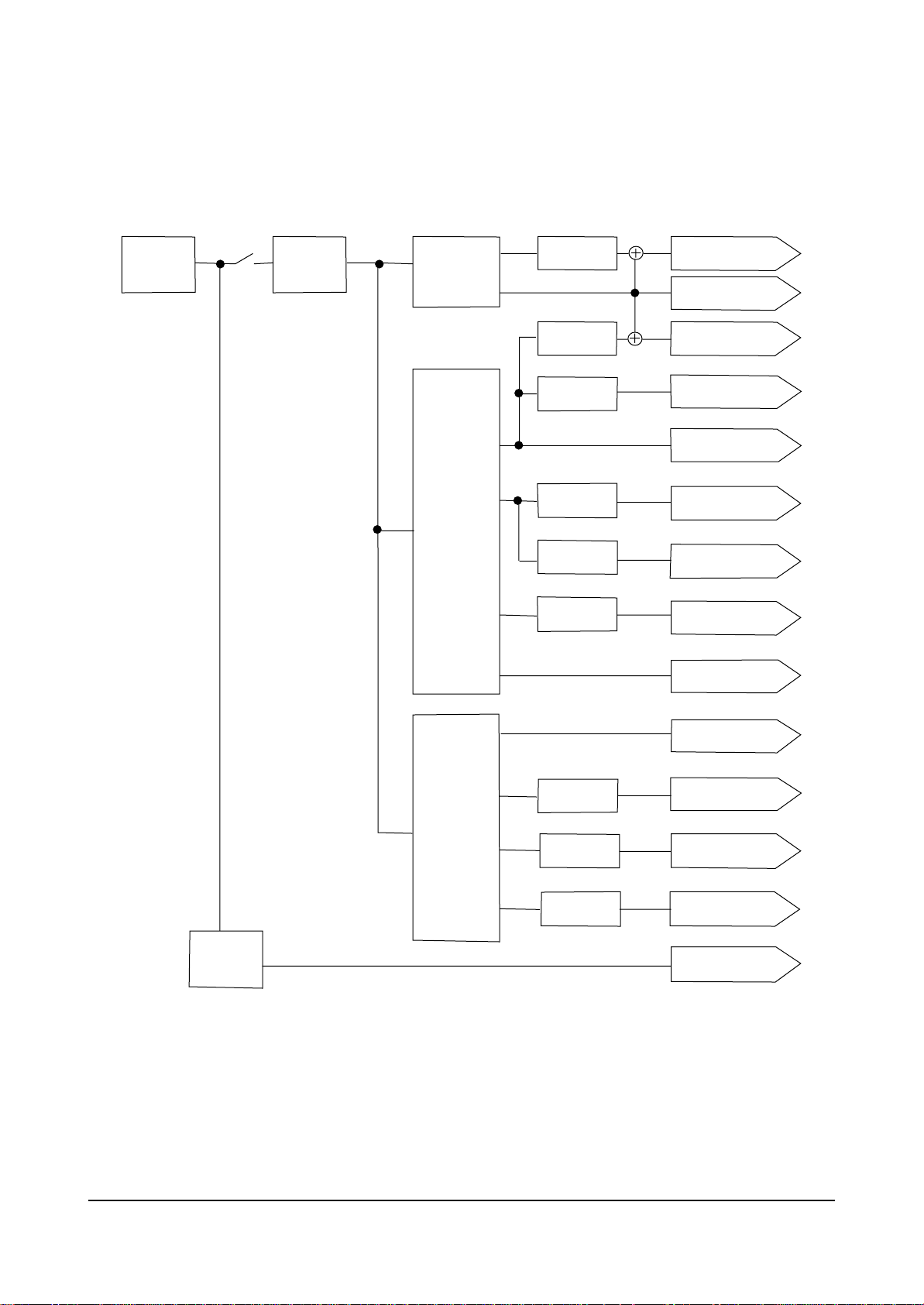
6-4 Scaler Board Block Diagram & Description
6-4-1 General Signal Process B/D
Ke y p a d
Exte r nal
IR
Module
Sub PCB for
Exte rna l Cont rol
MCLK DCLK
LVDS OUT
(63LVDM83A)
RGB,H/V
CLK, DE
2000. 05. 06
designed by K.H.I
PDP
Logic B’d
RGB,H/V
CLK, DE
Flash Mem.
(M29W800T)
(ICS501,502 )
C
2
Progr ammable P LL
OSD Mixe r,
(Imag e S c a ling ,
Image Processor
PW364
with CPU
Frame Rate Conversion)
M
CI
EEPRO
2
(24C16)
I
YUV,
2H/V,
AVO
RGB,
GCLK
Puls e Gen.
YPbP r RGB
(M4A3 32/32)
SCP
(CXA2101)
YPbPr
RGB,H/V
GFBK
DTV(480p,720p,1080i)DVD(480p)
RGB,H/V
Analog Switch
C
2
I
(BA7657)
with PLL
A/D conver ter
RGB
Analog Switch
RGB,H/V
RGB,H/V
C
2
I
(SDA9400)
Interlace to
Progre ss ive
YUV,H/ V
C
Decoder
2
(VPC3230)
Main Vid e o
I
D/A
(SDA9280)
C
2
I
Sand Castle
13.5MHz
27MHz
YPbPr
H/V (480P)
H/V
C
2
I
HD Interface
DVD
3D
COMB
YPbPr(480i)
C
2
I
(AD9884)
(BA7657)
SRAM
(KM616V1000)
RTC
(PCF8563)
CS
(LM1881)
Sync Sepe ra te
H/V
G(SOG)
DDC IC
V
DDC
(24LC21)
SDA/SCL
RXD/T X
D
(MAX232A)
Serial Interface
Aud io Am p.
( TA1101 )
Sub PCB for
Aud io
C
2
I
Aud io
Processor
( TDA7429 )
Video
(CVBS)
(Y/C)
S- Video
Input
(Y,Pb,Pr)
Comp onen t
DTV YPbPr
(480p,720p,1080i)
DVD YPbPr
(480i,480p)
PC RGB HV
(15 pin)
PC Input
VGA to S XGA
Vf: 56 to 75Hz
Hf: 3 1 to 80 kHz
RS232C
OUT
(L/R)
Audio In
RS232C IN
Page 60

Circuit Operation Description
6-38 Samsung Electronics
6-4-2 Description in Signal Process Block
3D COMB FILTER : This 3D Comb Filter is used to improve noise and picture quality by three-dimensionally adjusting the
signal from the Input Video jack. The input signal is received from CVBS and the picture is digitally
improved via A/D Conversion and FIELD MEMORY. And then the signal is output as the ANALOG YC signal.
VPC3230 : This functions as a video decoder, which can receive all of the YC, YUV, CVBS inputs.
In addition, this converts Y/C into YUV after receiving 3D Comb Output Y/C, S-Vido Y/C, and DVD YUV.
VIDEO DOUBLER : Usually, the current video image adopts the INTERLACE Scanning system and it has poor video because of
Flicking on the screen. Using the SDA9400 , INTERLACE is converted into PROGRESSIVE in order to improve
the quality of video.
VIDEO PROCESSOR : Since the HD modes like 1920*1080I have higher video bandwidth than the existing video signals, the
ordinary decoder like VPC3230 can't handle those modes. PC has higher bandwidth of video signal than TV
and the RGB video format.
Therefore, if the HD signal can be converted into the RGB signals, the TV video signal can have the same
processing as the PC VIDEO signal. CXA2101 developed by SONY is used to convert YPbPr into RGB.
CXA2101 converts both DTV signals and all the SD signals processed in the sequence of SDA9400 then
SDA9280 into RGB.
This processor performs some user control functions, such as tint, color, and sharpness.
Also, it controls high light gains low light offsets when doing white balance adjustments.
ANALOG SWITCH : The video decoder like VPC3230 has a built-in video switch that assigns one signal out of various
received inputs, though most of ICs for PC are designed so that they support only one source because of
less necessity of simultaneously processing the multi inputs. To process the input source of MULTI
(PC&HD), therefore, a function of selecting an input should be externally added; as is performed by ROHM's
BA7657F. PW364 transmits a signal determining which input is selected.
ADC : A device that converts the input RGB signals into the 8bit DIGITAL RGB signals.
In case of white balance adjustments, this device sets the color temperature by controlling R/B gains and
R/B offsets.
PW364 : PW364 is a multi-functional scaler which one chip has video signal scaling, 8086 CPU, 4M BYTE VIDEO
MEMORY functions. The PC and Video input signals are received from GRAPHIC PORT and VIDEO PORT,
respectively.Its main functions include UP/DOWN SCALING, PIP, ZOOM, GAMMA CORRECTION,
Compensation of GEOMETRIC DISTORTION, powerful GRAPHIC OSD.
FIRMWARE : Mounted is a software that is used for system control by operating 8086 built in PW364. A 4MBIT FLASH
ROM is mainly used, but one up to 8MBIT can be used according to PROGRAM and capacity of OSD DATA.
The system is easy to maintain because programming can be re-done at any yime using the FLASH ROM.
Page 61

Circuit Operation Description
Samsung Electronics 6-39
6-5 IC Line-Up
6-5-1 IC LINE UP
BA7657
CRYSTAL
ANALOG
DIGITAL
CLOCK
AD9884
CXA2101
TOLOGIC
LVDS OUT
90CF385
67.4MHZ
VIDEO
CLK
16 .25
7
ICS501
130MHZ67. 4MHZ
PW364
27MHZ
20 .25
ICS502
SDA9400
27MHZ
FROMSMPS
29LV16
616V100
MAX232
13.5
MHZ
CONTROL
PWR
RMC/LED
BA7657
RGB1 RGB2
D_SUB
DTV
M4A3
DVD(480I)
K4E
151612D
Pr/RVH
B
SDA9280
20
20.2
5
UPD
64082
COM POSITE
Y/GPb/
VPC3230
Y/C
VIDEO
TO SOUND
Y/C
S_VIDE
O
Page 62

Circuit Operation Description
6-40 Samsung Electronics
6-5-2 PIN Description
Pi n No. Pin Name Pin Na me Pin Name Pin Name Pin Na me Pin Name
1 DGND
2 GND SCL KEY1
3 TxOUT0 - / RxIN0
4+/
5 REL_SW R 1 LED G
6 TEMP DET T2
7FANDETR2
8 GND
9AMPMUTE1
10 12V GND
11 12V
12 A6V
13
14
15 T xCLKOUT-/ RxCLKIN16
TxCLKOUT-/ RxCLKIN
17
18
19
20
21 NC
22 NC
23 NC
24 NC
25 NC
26 NC
27 NC
28 NC
29 NC
30 NC
31 NC
DGND
TxOUT0 RxIN0
DGND
DGND
TxOUT1 - / RxIN1
TxOUT1 RxIN1
TxOUT1 - / RxIN1
TxOUT1 RxIN1
TxOUT3 - / RxIN3
TxOUT3 RxIN3
+/
DGND
DGND
+/
DGND
DGND
DGND
DGND
+/
+
ST5V SDA ST5V
GND
D5V T1 LED R
GND
GND
GND
GND
KEY1
KEY1
KEY4
GND
KEY4
GND GND
KEY4
RMC S IG
Page 63

Circuit Operation Description
Samsung Electronics 6-41
6-6 Main I/O signal pules and voltages
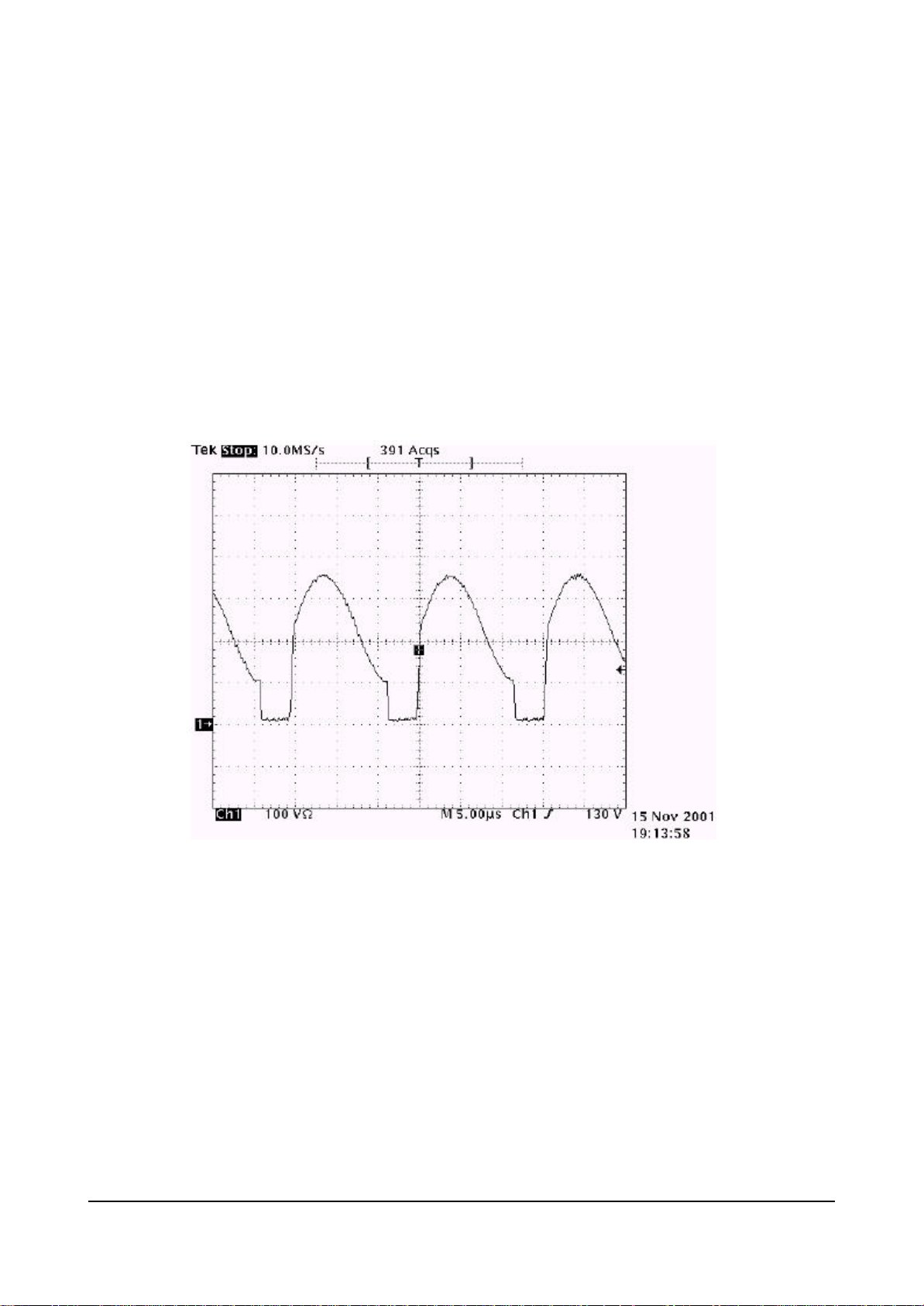
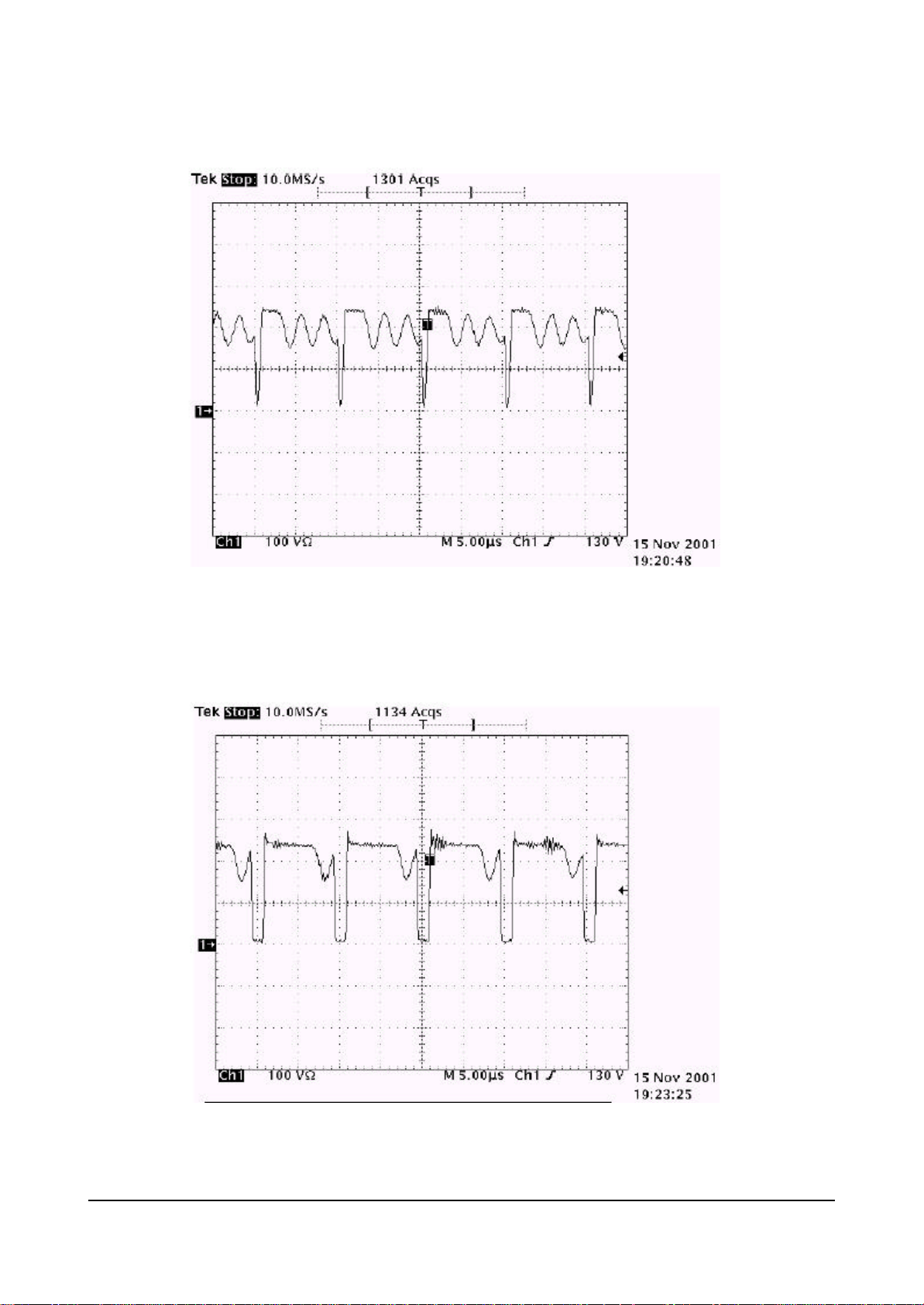
6-6-1 Signal Pulses of Image Board(Input Signal Conditions : 7 Color bar)
* 9C55 VIDEO INPUT *3D COMB P88 VIDEO INPUT
* 3D COMB P84 Y OUTPUT *3D COMB P83 C OUTPUT
* 3U1(VPC3230) PIN75 Y_IN * 3U1(VPC3230) PIN72 C_IN
Page 64

Circuit Operation Description
6-42 Samsung Electronics
* 3U1(VPC3230) PIN40 Yo_OUT * 3U1U(VPC3230) PIN56 HS_OUT
* 3U1(VPC3230) PIN57 VS_OUT * 3U1(VPC3230) PIN27 LLC2_OUT
* 3U1(VPC3230) PIN28 LLC1_OUT
Page 65

Circuit Operation Description
Samsung Electronics 6-43
* 3U2(SDA9280) PIN47 V_Y_OUT * 3U2(SDA9280) PIN51 V_Pr_OUT
* 3U2(SDA9280) PIN54 V_Pb_OUT * 2U2(CXA2101) PIN39 B_OUT
* 2U2(CXA2101) PIN37 G_OUT * 2U2(CXA2101) PIN35 R_OUT
Page 66

Circuit Operation Description
6-44 Samsung Electronics
* 1U1(AD9884) PIN:115 PCLK_OUT * U29(AD9884) PIN7 R_IN
* U29(AD9884) PIN95 ROUT_ODD * U29(AD9884) PIN105 ROUT_EVEN
Page 67

Circuit Operation Description
Samsung Electronics 6-45
* 2U2(CXA2101AQ) PIN5 DTV.Y_IN * 2U2(CXA2101AQ) PIN4DTV.Pb_IN
* 2U2(CXA2101AQ) PIN3 DTV.Pr_IN * 2U2(CXA2101AQ) PIN35 DTV.R_OUT
* 2U2(CXA2101AQ) PIN37 DTV.G_OUT * 2U2(CXA2101AQ) PIN39 DTV.B_OUT a
Page 68

6-46 Samsung Electronics
MEMO
Page 69

Troubleshooting
Samsung Electronics 7-1
7. Troubleshooting
7-1 No Raster(Board Change in PDP Monitor)
ST - BY Mode(LED:RED)
norma l
Power On 8J1 Re place s caler B’d
(LED:GREEN) Output
norma l
SMPS AC
Abnormal
ST 5V
Abnormal
Abnormal Abnor mal
Output Voltage Input
norma l
norma l
Logic Connect Powe r Re place SMPS
LED Lig h t- o n
(Po w e r,Sink)
norma l
Abnormal
Re place Logic B’d
X- B’ d Connect Power
norma l
or Go to P age 7- 2
Cha n g e Fuse
X- B’ d
Output
norma l
Abnormal
Repla ce X- B’d
Y- B’ d Connect Power
Y- B’ d
Abnormal
Repla ce X- B’d
Output
norma l
Repla ce Panel
Page 70

7-2 Samsung Electronics
Alignment and Adjustments
7-2 No Raster in Scaler Board
Chec k Out p ut Da t a of 5J1
Abnormal
Nor mal
Chec k Log ic B’d
Check Input Signal of 5U1 LVDS IC
Pin 2 7(LHS),28(LVS),32(CLK)
Abnormal
Check Output Signal of 1U1 AD9884
Pin 115(CLK), 85 (G7), 1 05(R7),65(B7)
Abnormal
Check Input Signal of 1U1 AD9 884
R,G,B IN AND H,V IN
Abnormal
Check Output Signal of 3U3 SDA9280
Pin 47(Yout),
Nor mal
Nor mal
Nor mal
Nor mal
Chec k 5 U1
LVDS IC
CHECK
PW364
CHECK 1U1
AD9884
CHECK 2U2
CXA2 1 0 1
Abnormal
Check Input Signal of 3U1 VPC323 0
Pin 75(Y IN)
Abnormal
Check Input Signal of U38 uP D6 4082
Pin 8 8 (CVBS in)
Nor mal
Nor mal
Chec k 3U1 ,
3U2 OR3U3
CHECK
UPD64 0 8 2
CHECK INPUT SIGINAL
Page 71

Troubleshooting
Samsung Electronics 7-3
7-3 Partly no screen
Page 72

Troubleshooting
7-4 Samsung Electronics
7-4 63”HD s1.0 Logic Main Board T/S
If the PDP unit and the logic board operates properly, the operation LED of Figure 1 would blink at about
1 second interval.
If the unit is out of order, check the status of the operation LED through eye-inspection first.
If the behavior of the operation LED is different from that of normal state, you have to replace the board.
To check the trouble on the board, complete the following logic board test procedures described below.
Required testing equipment : - Oscilloscope (digital 400 MHz with more than 3 channels)
- Multi-meter
Other equipment : - DC power supply (5V: 1EA)
- Sub-PCB ASS'Y for JIG: 1 EA
Perform eye-inspection and short circuit inspection on the power stage of the logic board to be
examined. If no problem is found, perform the following examinatios on the board in order.
Change the clock setting of the logic board to internal.
Connect the power (5V) to LD1, and check that the LED (LD2000) on the top left of the board
blinks at about a 1 second interval.
If the logic board is out of order, the LED will blink too fast or not be lit at all.
If no problems were found in the above examination, connect the logic main board with
CN2003(13P), LY2000(40P), LE2001(40P), LE2002(40P), LE2003(40P), LG2001(40P), LG2002(40P)
and LG2003(40P) using the connection cable.
Set the oscilloscope at 4ms/div and 5V/div.
Check Drive Y s/w, Drive X s/w and the address signal in order.
Set Probe 1 of the oscilloscope to the trigger signal and connect it to TP41 of the logic board.
Measure the waveform at each test point on the board, and compare it with the appended
waveforms. Make sure that you examine the waveforms of all the test points.
Turn off the power supply switch after the test, and disconnect the connector.
Page 73

Troubleshooting
Samsung Electronics 7-5
POL(LE2001, LE2002, LE2003, LG2001, LG2002, LG2003 : 25)
DATA(LE2001, LE2002, LE2003, LG2001, LG2002, LG2003 6~11, 15~20, 28~33
LG2003, LE2003 : 35~40)
Page 74

Troubleshooting
7-6 Samsung Electronics
CLK(LE201, LE2002, LE2003, LG2001, LG2002, LG2003 : 13,22
STB(LE2001, LE2002, LE2003, LG2001, LG2002, LG2003 : 24)
Page 75

Troubleshooting
Samsung Electronics 7-7
Y7
Y5
Page 76

Troubleshooting
7-8 Samsung Electronics
Y11
Y9
Page 77

Troubleshooting
Samsung Electronics 7-9
Y15
Y13
Page 78

Troubleshooting
7-10 Samsung Electronics
Y19
Y17
Page 79

Troubleshooting
Samsung Electronics 7-11
Y23
Y21
Page 80

Troubleshooting
7-12 Samsung Electronics
Y28
Y25
Page 81

Troubleshooting
Samsung Electronics 7-13
Y32
Y30
Page 82

Troubleshooting
7-14 Samsung Electronics
X2
Y34
Page 83

Troubleshooting
Samsung Electronics 7-15
X6
X4
Page 84

Troubleshooting
7-16 Samsung Electronics
X10
X8
Page 85

Troubleshooting
Samsung Electronics 7-17
7-5 Inspection of the Driver Board
7-5-1 Y buffer
- To check if there is a problem with the Y main, first examine whether the Y buffer operates normally.
- Disconnect the connector between the Y main and the Y buffer.
- Diode-check the area between OUTL and OUTH to make sure that the flow of the voltage
remains at 0.4V~0.5V.
- The impedance between the two ends must be more than a few k Ω.
OUT L OUTH
OU TL
OU TH
OU TL
OU TH
OU TL
OU TH
OU TL
OU TH
OU TL
OU TH
OU TL
OU TH
TP
OU TL
OU TH
OU TL
OU TH
TP
Page 86

Troubleshooting
7-18 Samsung Electronics
7-5-2 Y Main
- Connect the Y main to the Y buffer, and check that the output of the TP in the Y buffer
appears as noted in Appendix 1 when power is applied.
CN5401
-
Panel
CN5402
-
Panel
CN5404
CN5406
CN5405
CN5407
CN5409
CN5007
CN5001
CN5006
CN5005
CN5008
-
Power
CN5003
CN5403
-
Panel
CN5408
CN5004
TP
CN5002
Signal
-
Page 87

Troubleshooting
Samsung Electronics 7-19
7-5-3 X
-Check that the output of either Out 1 or Out 2 on the X board appears as noted in Appendix
2 when power is applied.
CN4004
-
Power
CN4009
X- OUT1
CN4005
-
Signal
CN4008
CN4007
X- OUT1
CN4006
Page 88

Troubleshooting
7-20 Samsung Electronics
Appendix 1
■ Y Output Waveform
- The status of the waveform when it is not connected to the panel.
❈ Make sure there is only one scan waveform in the output!!
Y Output Waveform (200us/div, 100V/div)
❈ Be sure to check that the energy recovery software is operating!!
Page 89

Troubleshooting
Samsung Electronics 7-21
Appendix 2
■ X Output Waveform
- The status of the waveform when it is not connected to the panel.
X Output Waveform (200us/div, 100V/div)
❈ Be sure to check that the energy recovery software is operating!!
Page 90

Troubleshooting
7-22 Samsung Electronics
7-6 No audio is sounded and video is displayed properly
Page 91

Exploded View and Parts List
Samsung Electronics 4-1
4. Exploded View and Parts List
4-1 HPL63H1X/XAA MODULE
You can search for the updated part code through ITSELF web site.
URL : http://itself.sec.samsung.co.kr
[17]
[14]
[27]
[3]
[24]
[20]
[13]
[13]
[5]
[12]
[26]
[23]
[4]
[6]
[9]
[7]
[2]
[25]
[10]
[11]
[4]
[8]
[3][21]
Page 92

Exploded View and Parts List
4-2 Samsung Electronics
J
6
1
0
5
200
HC,
TY
2
1
1
2
1
1
1
1
1
1
1
2
2
1
2
1
1
1
1
1
1
1
1
DP63HW01A 63, HW,ASYM,DUAL, 300x340x380, 0~0, 1443x833
LJ93-00050A 63HD
LJ61-00714A 63HD, SECC, T2. 0
NO PART DESCRI PTI ON CODE NO SPE CI FI C ATI ON Q’
LJ61-00552A 5 0HD, AL DI ECASTI NG,
PAN EL- PD P
ASSY- CHA SSIS, BASE
BRACK ET- WALL
GUI DE- STAND
1
2
3
4
LJ61-00855A 63HD, SECC, T1. 0, -, -, -, -
BRACK ET- PO W ER
5
LJ92-00540B 63HD, LJ41-00940B, - , SDI, E-BUFFER, 438X45XT1. 6MM,-,-,
LJ92-00541B 63HD, LJ41-00941B, - , SDI, F-BUFFER, 433X45XT1. 6MM,-,-,
LJ92-00542B 63HD, LJ41-00942B, - , SDI, G-BUFFER, 438X45XT1. 6MM,-,-,
LJ92-00543B 63HD, LJ41-00943B, - , SDI, H BUFFER, 438X45XT1. 6MM,-,-,
LJ92-00544B 63HD, LJ41-00944B, - , SDI, I BUFFER, 433X45XT1. 6MM,-,-,
LJ92-00545B 63HD, LJ41-00945B, - , SDI, J BUFFER, 438X45XT1. 6MM,-,-,
LJ92-00674A 63HD, LJ41-01057A, - , SDI , LOGIC MAIN, 320X190XT1. 6MM,-
LJ44-00039A PDP-PS-63A, 110 ~ 130V, 47HZ-63HZ
LJ92-00603A 63HD, LJ41-01230A, 63HD- YM-1.0,SDI,YMAIN, 315X190XT1
LJ92-00552B 63HD, LJ41-01112A, 63HD- XM-1.0,SDI,X-MAI N, - , CLAS S B,
LJ92-00547A 63HD, LJ41-00947A, - , SDI , Y-BUFFER LO, 375X60XT1.6MM,-
LJ92-00546A 63HD, LJ41-00946A, - , SDI , Y-BUFFER UP, 375X60XT1. 6MM,-
LJ92-00549A 63HD, LJ41-00949A, - , SDI , X-BUFFER LO, 375X60XT1.6MM,-
LJ92-00548A 63HD, LJ41-00948A, - , SDI , X-BUFFER UP, 375X60XT1. 6MM,-
LJ92-00655A 63HD, -, -, SDI, AC LI NE , 193. 5X146XT1. 6MM,-,-,-
LJ92-00551A 63HD, LJ41-00951A, - , SDI , Y-SUB, 410X30X1. 6MM,-,-,-
LJ92-00550A 63HD, LJ41-00950A, - , SDI , X-SUB, 410X25X1. 6MM,-,-,-
ASSY- PCB, B UFFE R( E )
ASSY- PCB, B UFFE R( F)
ASSY- PCB, B UFFE R( G)
ASSY- PCB, B UFFE R( H)
ASSY- PCB, B UFFE R( I )
ASSY- PCB, B UFFE R( J)
ASS Y- P CB, LOGI C( M AI N)
SMPS
ASSY-PCB, Y(MAI N)
ASSY-PCB, X(MAI N)
ASSY- PCB, B UFFE R( L )
ASSY- PCB, B UFFE R( U)
ASSY- PCB, B UFFE R( L )
ASSY- PCB, B UFFE R( U)
ASSY- PCB, LI N E (FI LT E R)
ASSY- PCB, SUB
ASSY- PCB, SUB
6
7
8
9
10
11
12
13
14
15
16
17
18
19
20
21
22
Page 93

Samsung Electronics 4-3
Exploded View and Parts List
4-2 HPL63H1X/XAA MONITOR
[5]
[8]
[22]
[30]
[32]
[4]
[32]
[3]
[15]
[5]
[12]
[13]
[1]
[2]
[33
Page 94

Exploded View and Parts List
4-4 Samsung Electronics
S
C
E
W
M
A
H
I
E
6
0
0
-
0
0
67W
,
+,8
,
Z
Y
ELM
2
0
TY
2
1
1
1
2
1
1
1
1
1
1
1
1
1
6
2
1
1
1
1
1
3
1
63, HW,ASYM, DUAL, 300x340x380, 0~0, 1443x833
LJ91-00472A 6 3HD, ABS, L/ GRAY, S EC, - , - , -
ASSY- CABINET , FR ON T
GLASS- FI LTER LJ64-00052A 63HW, 1363A- 202S1-A, T3. 8, W1442, L832, -, - , 0. 1OHM3HO LD ER- FI TER, TOP LJ61- 00316B 63HD, AL, T1. 5, -, L1422, -, -4HOLDER- F I LTE R, BOT LJ61-00317B 63HD, AL, T1. 5, -, L1422, -, -5HO LD ER- FI TER, SI DE LJ61-00318B 63HD, AL, T1. 5, -, L742, - , -6ASSY PCB CON T ROL LJ92-00538A 63HD, -, 63HD-KP- 1. 0, SDI , KEY PAD, 217X15XT1. 6MM,-,-,-
1
NO PART DESCRI PTI ON CODE NO SPE CI FI C ATI ON Q’
2
BUTTON- CONTROL LJ64-00030A 42"S1. 0 ABS( V0)
7
LJ92-00592A 63HD, -, -, SDI, SCALER BOARD, - , D52A, HPL5025M,-,-
PM63HW003A
MODULE
ASSY-PCB, VIDEO
8
LJ92-00586B 63HD, - , 63HD- ST- 1. 0, SDI , SDI , SPK TERM,-,CLASS B,-,-
LJ92-00593A 6 3HD, - , - , S DI , AUDI O SOUND, - , HPL50 2 5 M X/ XAA, D5 2 A, - , -
ASSY- PCB, TE RMI NAL
ASS Y- P CB, AUI DO
HO LD ER- CABI NET, TL LJ61- 00733A 63HD, SPC , T1. 6, -, -, - , -13HOLDER- CABI NE T LJ61-00715A 63HD, SPC, T1.6, - , - , - , NI14HO LD ER- CABI NET, TM LJ61-00789A 50HD, SPC, T1. 6, - , - , - , -15HOLDER- CABI NE T, SI DE LJ61-00734A 63HD, SPC, T1. 6, - , - , - , -16HOLDER- CABI NE T, SI DE( M ) LJ61-00735A 63HD, SPC, T1. 6, - , - , - , -17BRACK ET- RMC LJ61- 00324A SPD-42P1S,SECC,T1.0,-,-,-,-18ASSY PCB CON T ROL LJ92-00539A 63HD, -,63HD-RM-1.0,SDI,R/MODULE,90X27X1. 6MM,-,-,-19COV ER- BACK , TERM IAL LJ63-01065A 63HD, AL, T1. 5, -, -, -, -, BLK, -20COV ER- BACK LJ63-01064B 63HD, AL, T1. 5, -, -, -, -, BLK, -
9
10
11
12
6006-001035 WSP, PH, +, M3, L8, ZPC ( Y EL) , SM10C
SCREW-ASS’ Y, M ACH
21
SCREW- TAPPI NG 6002-001142 TH,+,2,M3. 5, L10, ZPC( YEL) , SWRCH1 8 A
22
Page 95

Samsung Electronics 4-5
Exploded View and Parts List
4-3 For assy replacement, code number and description by assy
In order to replace a broken part, please see the figure below and makea request using
the assy code number of a spec assy neccessary for replacement.
5
6
7
10
8
14
18
13
10
17
3
4
9
12
2
15
8
16
1
9
11
Page 96

Exploded View and Parts List
4-6 Samsung Electronics
1
Q’TY
1
1
1
1
1
1
2
2
1
1
1
1
1
1
2
1
LJ92-00540B 63HD, LJ41- 00940B, - , SDI, E-BUFFER, 438X45XT1. 6MM,-,-,
LJ92-00541B 63HD, LJ41- 00941B, - , SDI, F-BUFFER, 433X45XT1. 6MM,-,-,
LJ92-00542B 63HD, LJ41- 00942B, - , SDI, G-BUFFER, 438X45XT1. 6MM,-,-,
LJ92-00543B 63HD, LJ41- 00943B, - , SDI, H BUFFER, 438X45XT1. 6MM,-,-,
LJ92-00544B 63HD, LJ41- 00944B, - , SDI, I BUFFER, 433X45XT1. 6MM,-,-,
LJ92-00545B 63HD, LJ41- 00945B, - , SDI, J BUFFER, 438X45XT1. 6MM,-,-,
LJ92-00674A 63HD, LJ41-01057A, - , SDI, LOGI C MAI N, 3 2 0 X1 90 XT1. 6 M M,-
LJ44-00039A PDP-PS- 63A, 110 ~ 130V, 47HZ- 63HZ
LJ92-00603A 63HD, LJ41-01230A, 63HD- YM-1.0,SDI,YMAI N, 3 1 5 X1 9 0 XT1
LJ92-00552B 63HD, LJ41- 01112A, 63HD-XM-1.0,SDI,X-MAI N, - , CLAS S B,
LJ92-00547A 63HD, LJ41-00947A, - , SDI, Y- BUFFER LO, 375X60XT1. 6MM,-
LJ92-00546A 63HD, LJ41-00946A, - , SDI, Y- BUFFER UP, 375X60XT1. 6MM,-
LJ92-00549A 63HD, LJ41-00949A, - , SDI, X- BUFFER LO, 375X60XT1. 6MM,-
LJ92-00548A 63HD, LJ41-00948A, - , SDI, X- BUFFER UP, 375X60XT1. 6MM,-
LJ92-00655A 63HD, -, - , SDI , AC LINE , 193. 5X146XT1. 6MM,-,-,-
LJ92-00551A 63HD, LJ41-00951A, - , SDI, Y- SUB, 410X30X1. 6MM,-,-,-
LJ92-00550A 63HD, LJ41-00950A, - , SDI, X- SUB, 410X25X1. 6MM,-,-,-
LJ92-00592A 63HD, -, - , SDI , SCALER BOARD, - , D52A, HPL5025M
ASSY- PC B, BUFFE R( E)
ASSY- PC B, BUFFE R( F)
ASSY- PC B, BUFFE R( G)
ASSY- PC B, BUFFE R( H)
ASSY- PC B, BUFFE R( I )
ASSY- PC B, BUFFE R( J)
ASS Y- PCB, LOGI C( M AI N)
SMPS
ASSY-PCB,Y(MAI N)
ASSY-PCB,X(MAI N)
ASSY- PC B, BUFFE R( L)
ASSY- PC B, BUFFE R( U)
ASSY- PC B, BUFFE R( L)
ASSY- PC B, BUFFE R( U)
ASSY- PC B, L I N E (FI LT E R)
ASSY- PC B, SUB
ASSY- PC B, SUB
ASSY PCB VIDEO
1
2
3
4
5
6
7
8
9
10
11
12
13
14
15
16
17
NO PART DESCRI PTI ON CODE NO SPE CI FI CATI ON
18
Page 97

DDC/ADC/analog Connector
[ AD9884 INTERFACE PAR
T ]
ABO[7:0]
ARO6
ARO5
ARO3
ARO4
ARO[7:0]
ABO0
ARO7
ABO1
ABO7
ABO5
ABO4
ABO3
ABO6
ABO2
ARO1
ARO0
ARO2
ARE[7:0]
AGE[7:0]
ABE[7:0]
ABE3
AGE0
ARE7
AGE2
ARE3
ARE5
AGE3
ARE4
AGE5
AGE7
ABE1
ARE1
AGE6
ABE4
ABE0
AGE1
ABE6
ABE7
ARE2
ABE2
ARE0
ABE5
ARE6
AGE4
SR3
SQ1
SR6
SQ6
SQ18
SQ20
SR5
SR0
SR7
SR23
SR20
SQ10
SQ11
SR14
SR11
SQ5
SQ23
SQ7
SQ16
SQ22
SQ14
SR1
SR21
SQ9
SQ8
SR4
SQ4
SR15
SR9
SQ12
SR8
SR13
SR22
SQ3
SR12
SR16
SQ15
SR17
SR2
SQ0
SQ19
SQ21
SQ2
SR19
SR18
SQ17
SQ13
SR10
ARE1
ARE0
ARE2
ARE3
ARE4
ARE5
ARE6
ARE7
ABO2
ABO5
ABO7
ABO6
ABO4
ABO1
ABO0
ABO3
SOGREF
SQ22
SQ21
SQ7
SQ3
SQ2
SQ15
SR21
SR16
SQ18
SQ5
SR18
SR10
SR0
SQ23
SQ0
SR14
SR6
SQ11
SQ6
SR7
SR4
SQ14
SQ13
SQ4
SR5
SR3
SR2
SR1
SR22
SR8
SQ19
SQ9
SQ8
SR23
SR19
SR11
SQ20
SQ17
SQ16
SQ10
SR9
SQ12
SQ1
SR13
SR17
SR12
SR20
SR15
SR13
SR20
SR8
SR22
SR3
SR5
SR1
SR9
SR7
SR0
SR4
SR18
SR19
SQ13
SQ0
SR14
SQ18
SR10
SQ23
SR6
SQ10
SQ5
SQ6
SR23
SQ15
SQ2
SQ7
SQ11
SQ4
SQ12
SR2
SR16
SR21
SQ19
SQ17
SQ3
SQ21
SR11
SQ14
SQ22
SQ9
SQ16
SQ8
SQ20
SQ1
SR12
SR15
SR17
AGE0
AGE1
AGE2
AGE3
AGE4
AGE5
AGE6
AGE7
ABE1
ABE2
ABE3
ABE4
ABE5
ABE6
ABE7
ARO6
ARO7
ARO5
ARO2
ARO3
ARO0
ARO4
ARO1
ABE0
AGO7
AGO0
AGO4
AGO5
AGO2
AGO2
AGO3
AGO6
AGO7
AGO4
AGO1
AGO[7:0]
AGO3
AGO6
AGO1
AGO5
AGO0
SOGREF
ABO7
ABO2
ABO1
ABO5
ABO0
ABO3
ABO4
ABO6
AGO2
AGO5
AGO6
AGO4
AGO1
AGO0
AGO3
AGO7
ARO6
ARO3
ARO4
ARO5
ARO0
ARO2
ARO1
ARO7
ABE2
ABE5
ABE6
ABE4
ABE1
ABE0
ABE3
ABE7
AGE6
AGE3
AGE4
AGE5
AGE0
AGE2
AGE1
AGE7
ARE3
ARE6
ARE5
ARE7
ARE1
ARE2
ARE0
ARE4
ADVCC
VPLL
VPLL
3.3V_A
3.3V
3.3V_A
ADVCC
3.3V_A
+5V
VPLL
ADVCC
ADVCC
TP212
1U2
2
1
4
5
6
3
nr
gnd
out
in
err
*sd
TP252
TP4
TP253
1C34
10uF/16V
TP514
TP224
1C31
104Z(OPEN)
TP254
1C5
10uF/16V
TP3
TP255
TP256
1C2
102J
1U1
AD9884
1
2
3
4
5
6
7
8
9
10
11
12
13
14
15
16
17
18
19
20
21
22
23
24
25
26
27
28
29
30
31
32
33
34
35
36
37
38
39404142434445464748495051525354555657585960616263
64
102
101
100
128
127
126
125
124
123
122
121
120
119
118
117
116
115
114
113
112
111
110
109
108
107
106
105
104
103
99
98
97
96
95
94
93
92
91
90
89
88
87
86
85
84
83
82
81
80
79
78
77
76
75
74
73
72
71
70
69
68
67
66
65
nc1
nc2
nc3
vdd1
gnd1
gnd2
RAIN
vdd2
gnd3
vdd3
vdd4
gnd4
gnd5
SOGIN
GAIN
vdd5
gnd7
vdd6
vdd7
gnd8
gnd9
BAIN
vdd8
gnd10
vdd9
gnd11
CKINV
CLAMP
SDA
SCL
A0
A1
PVCC1
PVCC2
gnd12
nc4
nc5
nc6
gnd13
HSYNC
COAST
gnd14
PVCC3
CKEXT
FILT
nc7
gnd15
PVCC4
gnd16
PVCC5
gnd17
gnd18
gnd19
VCC1
DBB7
DBB6
DBB5
DBB4
DBB3
DBB2
DBB1
DBB0
gnd20
VCC2
DRB0
DRB1
DRB2
vdd11
REFIN
REFOUT
PWRDN/
vdd10
gnd29
gnd28
gnd27
VCC8
gnd26
SOGOUT
HSOUT
DATACK/
DATACK
VCC7
gnd25
DRA0
DRA1
DRA2
DRA3
DRA4
DRA5
DRA6
DRA7
VCC6
gnd24
DRB3
DRB4
DRB5
DRB6
DRB7
VCC5
gnd23
DGA0
DGA1
DGA2
DGA3
DGA4
DGA5
DGA6
DGA7
VCC4
gnd22
DGB0
DGB1
DGB2
DGB3
DGB4
DGB5
DGB6
DGB7
VCC3
gnd21
DBA0
DBA1
DBA2
DBA3
DBA4
DBA5
DBA6
DBA7
1R9 304J
1NF1 SGM32F 1E104-2A
1
2
3
TP257
TP30
TP223
1C20 563K
TP258
1C1
104Z
1R7
472J
TP24
TP259
TP201
TP260
1C3
100J
1AR1 22 ohm
1
2
3
4 5
6
7
8
TP27
TP235
1C30
100J
1R4
102J
TP261
1C19
100J
TP14
TP222
TP262
TP29
TP202
1C28
104Z
TP263
1C18
102J
1C13
100J
TP264
TP31
TP234
1AR2 22 ohm
1
2
3
4 5
6
7
8
1C29
102J
TP265
1C9 563K
1C17
104Z
TP203
1AR3 22 ohm
1
2
3
4 5
6
7
8
TP221
Graphics Port
4U1A
PW364
U26
V24
V23
V25
V26
W25
W24
W23
H23
G26
H25
P23
P24
P25
P26
R23
B25
A26
D24
E23
C25
B26
C26
E24
R24
R25
R26
T23
T24
T25
T26
U25
F23
D25
D26
F24
E25
E26
F25
F26
D21
B22
C22
A23
B23
D22
C23
A24
L24
K26
L25
J26
K25
L26
L23
M25
H26
J25
J23
J24
M24
M26
GRE0
GRE1
GRE2
GRE3
GRE4
GRE5
GRE6
GRE7
GGE0
GGE1
GGE2
GGE3
GGE4
GGE5
GGE6
GGE7
GBE0
GBE1
GBE2
GBE3
GBE4
GBE5
GBE6
GBE7
GRO0
GRO1
GRO2
GRO3
GRO4
GRO5
GRO6
GRO7
GGO0
GGO1
GGO2
GGO3
GGO4
GGO5
GGO6
GGO7
GBO0
GBO1
GBO2
GBO3
GBO4
GBO5
GBO6
GBO7
GCLK
GPEN
GVS
GHS
GSOG
GFIELD
PLLCLK
GCLKOUT
GFBK
GREF
GBLKSPL
GCOAST
GHSFOUT
GADCCLK
1C11
104Z
TP266
TP33
1AR4 22 ohm
1
2
3
4 5
6
7
8
TP267
1R8
332J
1AR5 22 ohm
1
2
3
4 5
6
7
8
TP20
1C12
102J
TP268
TP35
TP204
TP233
1AR6 22 ohm
1
2
3
4 5
6
7
8
TP11
TP269
1C23
102J
TP205
TP34
TP220
1C6
100J
TP270
TP7
TP206
1C26
102J
TP271
1C22
104Z
TP207
1R1 470
TP272
TP232
1C25
104Z
TP273
1C24
100J
TP13
TP219
1R2
103J
TP274
1Q1
KSC1623_G
1
2 3
TP275
TP9
TP208
TP16
TP276
TP15
TP231
1C27
100J
1R10 334J
TP277
TP218
TP278
TP209
TP6
1C35
10uF/16V
TP279
TP17
TP280
TP230
TP281
TP217
TP282
TP19
1C4
10uF/16V
TP283
1C37
104Z
1C10 150J
TP229
TP12
1R5 472J
1C14 563K
TP21
1C38
104Z
TP216
1C16 150J
1AR7 22 ohm
1
2
3
4 5
6
7
8
TP236
1C15 563K
1AR12 22 ohm
1
2
3
4 5
6
7
8
TP237
1C39
104Z
1NF3
SGM32F1 E104-2A
1
2
3
1C21 150J
1AR9 22 ohm
1
2
3
4 5
6
7
8
TP238
1C32
393Z
TP23
TP228
1AR10 22 ohm
1
2
3
4 5
6
7
8
TP239
1C40
104J
1C36
104Z
TP615
TP18
TP215
1AR11 22 ohm
1
2
3
4 5
6
7
8
TP240
1NF21M2012-121
1 2
TP199
1AR8 22 ohm
1
2
3
4 5
6
7
8
TP241
TP25
TP28
TP616
TP32
TP242
TP200
TP26
TP227
1R3
201J(OPEN)
TP617
TP243
TP1
TP214
TP244
1C33
392J
1C8
104Z
TP245
TP210
TP22
TP246
TP10
TP226
1R11
104J
TP247
TP8
TP213
TP248
1C7
10uF/16V
1Q2
KSC1623_G
1
2 3
TP249
TP211
TP2
TP250
TP225
1R6 472J
TP251
TP5
SR[23:0]
SQ[23:0]
CLAMP
SDA
SCL
PCLK
CKINV
ADSEL
MHS
SOG
ARE[7:0]
AD_R_OUT
AD_G_OUT
AD_B_OUT
PCLK
SQ[23:0]
SR[23:0]
CDE
CLAMP
MHS
CVSYNC
MHSYNC
MCOAST
SOG
CHSYNC
CKINV
CKINV
MHSYNC
CLAMP
MCOAST
MHS
SQ[23:0]
SR[23:0]
ARO[7:0]
AGE[7:0]
AGO[7:0]
ABE[7:0]
ABO[7:0]
MHSYNC
MCOAST
ABO[7:0]
AGO[7:0]
ARO[7:0]
ABE[7:0]
AGE[7:0]
ARE[7:0]
10. Schematic Diagrams
Samsung Electronics
Schematic Diagrams
10-1
10-1 VIDEO
10-1-1 MAIN ADC (AD9884)
Page 98

Schematic Diagrams
10-2 Samsung Electronics
10-1-2 VIDEO D/A CONVERTER
V_Y/G
V_Pr/R
V_Pb/B
3C87
10uF/16V
TP297
3R61
3R71
3C88
10uF/16V
5V_A
3NF12
SGM32F 1E104-2A
1
3NF13
SGM32F 1E104-2A
1
3NF15
SGM32F 1E104-2A
1
3R52
101J
000J
101J
CLK2
IVCLK
IVVS
IVHS
TP284
3R63 R470J
TP285
3R68 R820J
TP286
3R70 R820J
5VCCI
3
2
2
2
3C85
5VCCA
3C89
104M
TP292
3NF14
1 2
M2012-121
104M
3
5VCC
TP293
3
3C90
104M
3R53 101J(OPEN)
3R56 101J
3R57 101J
3R58 101J
3R78 472J
TP291
3C86
104M
TP515
3R75
TP618
TP298
3R76
151J
SCL
SDA
3C76
152M
133J
3C91
104M
TP287 TP288 TP289
3C68
100M
3R62
3R64
3R69
622J
3R77
103J
3R59
3C69
3C70
100M
100M
TP517
101J
101J
3C73
3C74
100M
100M
TP290
424140393837363534333231302928
43
HS
VDD7
VSS9
TEST1
44
LF
45
Vcci
46
GNDY
47
YQ
48
Vcci1
49
VccA
50
GNDV
51
VQ
52
VccI2
53
GNDU
54
UQ
55
GNDA
56
Vref
57
Rref
58
Vcc
59
GND
60 10
VSS10 VDD3
VDD1
VDD2
VSS1V0V1V2V3
61626364656667
000J
VS
CLL
SDA
TEST
VSS8
3U3
SDA9280
V4
VSS2V5V6V7UV0
123456789
68
TP516
TP518
VSS7
TP294
VDD6
SCL
RES
SCA
UV1
INS
UV2
IVPEN
TP295
27
BLN
VSS6
VSS3
VSS4
VDD5
YUV7
YUV6
YUV5
YUV4
YUV3
YUV2
YUV1
YUV0
VSS5
UV7
UV6
UV5
UV4
UV3
VDD4
3R65 101J
3C77
104M
26
25
24
23
22
21
20
19
18
17
16
15
14
13
12
11
AY7
AY6
AY5
AY4
AY3
AY2
AY1
AY0
3C78
104M
AV7
AV6
AV5
AV4
AV3
AV1
AV0
RESETQ
TP296
3C79
104M
5AD
3C81
3C80
104M
104M
3AR22 120 ohm
1
2
3
4 5
3AR23 120 ohm
1
2
3
4 5
3AR24
120 ohm
1
2
3
4 5
3AR25 120 ohm
1
2
3
4 5
3C82
104M
3NF11
SGM32F 1E104-2A
3
3C84
3C83
10uF/16V
104M
YIN7
8
YIN6
7
YIN5
6
YIN4
YIN3
8
YIN2
7
YIN1
6
YIN0
UVIN7
8
UVIN6
7
6
UVIN5
UVIN4
UVIN3
8
7
UVIN2AV2
6
UVIN1
UVIN0
5V_A
1
2
YIN[7:0]
UVIN[7:0]
AY0
AY1
AY2
AY3
AY4
AY5
AY6
AY7
AV0
AV1
AV2
AV3
AV4
AV5
AV6
AV7
TP299
TP300
TP301
TP302
TP303
TP304
TP305
TP306
TP307
TP308
TP309
TP310
TP311
TP312
TP313
TP314
Page 99

Samsung Electronics
Schematic Diagrams
10-3
10-1-3 S-VIDEO &COMPONENT1 SIGNAL PROCESS
3R2 223J
TP619
3R6 101J
3R10 223J
3R11 101J
3R17
3R22 101J
3NF9 NFM40R0 1C101T1
1
2
TP322
3R44 101J
NFM40R0 1C101T1
3NF10
1
3C9 474Z
Pb/B
3C28
10uF/16V
Y/G
3C48 474Z
Pr/R
3.3V
3R43 101J
3J2
TSC7549
1 2
3 4
5 6
7 8
9 10
11
TP529
TP530
TP531
TP621
TP620
5VA
KSC1623_G
3Q1
1
TP622
3R7
2 3
3R8 470J
3R9
223J
471J
5VA
3Q2
1
KSC1623_G
3R13
223J
223J
1
3R23
223J
3
2
3
TP532
2 3
5VA
2 3
3R40
750J
TP533
3R15
471J
3Q3
KSC1623_G
3R25
471J
3C92
S1_DET
3C93
3R47
750J
TP623
3R14 470J
TP624
3R24 470J
1
+
22uF/16V
+
22uF/16V
2
3D2
DAN217
3
3R39 101J
TP629
1
2
3
TP630
TP315
3C10 224K
3C14
152K(OPEN)
TP316
3C27 224K
3C29 224K
3C33
152K(OPEN)
TP317
3C51 224K
3C56
152K(OPEN)
3D3
DAN217
3R46
3C15
+
47UF/16V
3C23
3C24
224Z
152K
3C35
3C36
224Z
152K
TP326
3C54
3C53
104M
104M
3NF8
SGM32F1 E104-2A
1
3C62
10uF
TP319
TP321
TP323
3C16
473J
3C25
391J
3C37
391J
47UF/16V
3.3VD
3C55
104M
3
2
C_OUTC_IN
D_PB
5VA
TP324
3C22
+
D_Y1 D_Y1
D_Y
3.3V_D
3NF6
SGM32F 1E104-2A
1
2
D_PR
UV0
UV1
UV2
UV3
UV4
UV5
UV6
UV7
Y0
Y1
Y2
Y3
Y4
Y5
Y6
Y7
TP318
223J
3R38
TP534
1
3R41
223J
TP320
3R45 223J
TP535
101J
1
3R48
223J
47UF/16V
TP325
5VA
3C34
+
47UF/16V
3
3C52
+
47UF/16V
TP339
TP340
TP341
TP342
TP343
TP344
TP345
TP346
TP347
TP348
TP349
TP350
TP351
TP352
TP353
TP354
5VA
3C61
100J
3Q5
KSC1623_G
Y_IN Y_OUT
2 3
3R42
471J
3Q6
KSC1623_G
2 3
3R49
471J
TP631
5VA
TP632
3C64 334Z
3C65 334Z
3C67 102K
3C1 270J
20.25MHz
3C3 270J
C1_OUT
Y1_OUT
3C30
+
D_PB
D_Y
D_PR
VSIN0
VSIN1
VSIN2
VSIN3
VSIN4
VSIN5
VSIN6
VSIN7
5V_A
3C31
224Z
TP328
TP327
3Y1
TP355
TP356
TP357
TP358
TP359
TP360
TP361
TP362
UV0
UV1
UV2
UV3
UV4
UV5
UV6
UV7
Y0
Y1
Y2
Y3
Y4
Y5
Y6
Y7
1 2
C_OUT
C1_OUT
Y_OUT
Y1_OUT
3R16 102J
UV[7:0]
3AR15 120 ohm
1
2
3
4 5
3AR18 120 ohm
1
2
3
4 5
3AR20 120 ohm
1
2
3
4 5
3AR21 120 ohm
1
2
3
4 5
Y[7:0]
5VA
3R1 330J
3C2 104M
3R4 101J
3R3 101J
TP625
TP626
VS
VSTBY
FPDAT
R2/CR2IN
ASGFNCVSUPCAP
TP524
3C43 224Z
TP525
TP519
3C44 224Z
3C45 152K
TP521
UVIN2
UVIN3
VDDD1
VSSS1
UVIN4
UVIN5
UVIN6
UVIN7
VDD3
VSS4
YIN0
YIN1
YIN2
YIN3
YIN4
YIN5
TP627
FSY/HC
MSY/HS
VPC3230
VSUPD
3C46 391J
3C58 104M
32
49
CLK2
AVO
GNDD
UNIN1
YIN6
TP628
6463626160595857565554535251504948474645444342
3U1
NC1
CLK5
XTAL2
XTAL1
ASGF1
65
GNDF
66
VRT
67
I2CSEL
68
ISGND
69
VSUPF
70
VOUT
71
CIN
72
VIN1
73
VIN2
74
VIN3
75
VIN4
76
VSUPA1
77
GNDA1
78
VREF
79
FB1IN
80
AISGND
B1/CB1IN
G1/Y1IN
R1/CR1IN
B2/CB2IN
G2/Y2IN
1234567891011121314151617181920212223
3C41 224Z
3C42 224Z
YSIN0
TP363
YSIN1
TP364
YSIN2
TP365
YSIN3
TP366
YSIN4
TP367
YSIN5
TP368
YSIN6
TP369
YSIN7
TP370
8
VSIN0
7
VSIN1
6
VSIN2
3.3VDD2
33
YSIN4
YSIN5
YSIN6
YSIN7
34
35
36
37
38
39
40
41
42
43
44
45
46
47
48
TP523
VSIN3
8
VSIN4
VSIN5
7
6
VSIN6
VSIN7
YSIN0
8
7
YSIN1
6
YSIN2
YSIN3
8
7
6
3R5 101J
INTLC
VSUPSY1
GNDCAP
SCL
3R18 101J
SCL
RESETQ
3R27 101J
UNIN0
RESET
VDDD5
YIN7
UV0
GNDSY1
SDA
3R19 101J
3R20 101J
SDA
RESETQ
CLK2
SYNCEN
3R28
3R29 000J
000J
SYNCEN
VSSS3
TP528
UV2
UV1
C0C1C2
RESQ
TEST
3R21 102J
3C47
104M
IVCLK
TP526
IVCLK
TP527
X2
X1/CLK2
3U2
SDA9400
CLK1
VDDD4
3R50 000J
UV3
C3
VGAV
YCOEQ
TP520
VDD2
CLKOUT
VDD4
VSS5
GNDC
VSUPC
FFIE
FFWE
HIN
3R30 101J
HIN
VSS3
VSSS2
VDDD3
UV4
UV5
C4C5C6
FFRSTW
FFRE
SDA
SCL
VIN
3R31 101J
3R32 101J
VIN
SDA
HOUT/HEXT
VDDD2
IVHS
UV7
UV6
41
C7
VSUPY
GNDY
GNDLLC
VSUPLLC
VSUPPA
GNDPA
FFOE
CLK20
24
3R33 101J
SCL
TEST
INTERACED
YOUT7
HREF
VOUT/VEXT
IVVS
IVPEN
IVPEN
Y0
Y1
Y2
Y3
Y4
Y5
Y6
Y7
LLC1
LLC2
171819202122232425262728293031
UVOUT0
YOUT6
646362616059585756555453525150
40
39
38
37
36
35
34
33
32
31
30
29
28
27
26
25
3.3VD
UVOUT1
UVOUT2
UVOUT3
UVOUT4
UVOUT5
UVOUT6
UVOUT7
VDD1
VSS2
YOUT0
YOUT1
YOUT2
YOUT3
YOUT4
VSS1
YOUT5
UV[7:0]
TP332
TP522
VIN
TP329
HIN
3.3VD
3C13 683M
3C32 473K
3C38 152K
YIN0
YIN1
YIN2
YIN3
YIN4
YIN5
YIN6
YIN7
IVHS
IVVS
TP37
TP39
TP41
TP43
TP45
TP47
TP49
TP51
TP53
TP55
TP56
Y[7:0]
TP330
TP331
TP336
IVFIELD
3C12 473K
3C11 102K
Y0
Y1
Y2
Y3
Y4
Y5
Y6
Y7
TP633
3NF3 10uH12
3NF4 10uH12
TP634
TP335
TP36
TP38
TP40
TP42
TP44
TP46
TP48
TP50
TP52
TP54
UVIN0
UVIN1
UVIN2
UVIN3
UVIN4
UVIN5
UVIN6
UVIN7
IVCLK
IVFIELD
IVPEN
3.3VDD1
UVIN0
UVIN1
16
15
UVIN2
14
UVIN3
13
UVIN4
12
UVIN5
UVIN6
11
10
UVIN7
9
8
7
YIN0
YIN1
6
5
YIN2
4
YIN3
3
YIN4
2
YIN5
1
YIN6
YIN7
TP334
UVIN[7:0]
YIN[7:0]
UVIN[7:0]
YIN[7:0]
3C39 220J
TP333
IVHS
IVVS
3.3V_D
3.3V_D
SYNCEN
CLK2
3C40 220J
3NF1 SGM32F 1E104-2A
1
3NF2 SGM32F 1E104-2A
1
CLK2
TP391
IVCLK
IVPEN
IVVS
IVFIELD IVFIELDOUT
IVHS
YIN0
YIN1
YIN2
YIN3
YIN4
YIN5
YIN6
YIN7
UVIN0
UVIN1
UVIN2
UVIN3
UVIN4
UVIN5
UVIN6
UVIN7
2
2
IVPENOUT
IVVSOUT
IVFIELDOUT
IVHSOUT
YOUT0
YOUT1
YOUT2
YOUT3
YOUT4
YOUT5
YOUT6
YOUT7
1
3NF5
M2012-260
1 2
3C49
10pF
3AR13 120 ohm
1
2
3
4 5
3AR14 120 ohm
1
2
3
4 5
3AR16 120 ohm
1
2
3
4 5
3AR17 120 ohm
1
2
3
4 5
3AR19 120 ohm
1
2
3
4 5
3
3C4
+
47UF/16V
3
3C17
+
47UF/16V
TP371
TP372
TP373
TP374
TP375
TP376
TP377
TP378
TP379
TP380
TP381
TP382
TP392
3C50
10pF
8
IVPENOUT
7
IVVSOUT
6
IVHSOUT
8
7
6
8
7
6
8
7
6
8
UVOUT4
UVOUT5
7
6
UVOUT6
UVOUT7
3C5
104M
3C18
104M
TP337
TP338
3C6
104M
3C19
104M
UVOUT0
UVOUT1
UVOUT2
UVOUT3
UVOUT4
UVOUT5
UVOUT6
UVOUT7
YOUT0
YOUT1
YOUT2
YOUT3
YOUT4
YOUT5
YOUT6
YOUT7
UVOUT0
UVOUT1
UVOUT2
UVOUT3
3.3VDD1
3C7
104M
3.3VDD2
3C20
104M
TP383
TP384
TP385
TP386
TP387
TP388
TP389
TP390
3C8
104M
3C21
104M
B16
VCLK
B17
VCLKEN
B18
VPEN
A21
VLAV
B21
VVS
A22
VHS
C21
VFIELD
A9
VR0
B10
VR1
A10
VR2
D11
VR3
C11
VR4
B11
VR5
A11
D12
C12
B12
A12
B13
A13
D14
C14
B14
A14
D15
C15
B15
A15
D16
C16
A16
VR6
VR7
VG0
VG1
VG2
VG3
VG4
VG5
VG6
VG7
VB0
VB1
VB2
VB3
VB4
VB5
VB6
VB7
4U1B
PW364
Video Po
rt
Page 100

Schematic Diagrams
10-4 Samsung Electronics
10-1-4 CONPONENT2 SIGNAL PROCESS
3.3V
2C95
10uF/16V
3.3V
5V_A
2NF9 NFM40R0 1C101T1
2J4
BNC
2NF13
S G M 3 2 F 1E104-2A
1
2
2NF1 SGM32F 1E104-2A
1
2NF2 SGM32F1 E104-2A
1
2
2
5V_A
2J1
BNC
1
3
3
2C1
104
2NF14
SGM32F1 E104-2A
1
2
TP537
3
2
2R85 750J
2C99
10uF/16V
3
2C2
104
3
2C96
104J
TP404
2C106
22uF/16V
8
4
2C97
104J
VCC
GND
+
TP397
ENVDD
TDI
PROTECT
TCK
TP154
TP155
1
NC
OUT
TP156
TP158
2C100
104
1
3
H1
H2
2C98
104J
EIO2
EIO3
Y1
27MHz
5
H1
1
3
TP536
2
2D8
DAN217
2R79 101J
2R97
OSC
2R98
R000J
TP426
2R100
R102J
TP657
2
2D14
DAN217
2R94 101J
2R73 101J
TP398
4847464544434241403938
2U7
R472J
TP393
TP394
TP395
TP396
H2
2R99
R000J
2D11
RLS4148
9VA3
TP542
TP538
2R82
223J
1
2
3
4
5
6
7
8
9
10
11
12
TP402
H2_OUT
21
H_IN V_IN
9VA3 9VA3 9VA3
2R76
223J
2Q6
1
KSC1623_G
2 3
2R88
471J
TP427
TP658
I/O 5
I/O 6
I/O 7
TDI
CLK0/I0
NC
GND
TCK
I/O 8
I/O 9
I/O 10
I/O 11
2R101
R000J
Y/G
2J2
BNC
13
11
14
2D12
RLS4148
PCHSYNC2
TP406
I/O 4
I/O 3
I/O 2
I/O 1
I/O 0
GNDNCVCC
M4A3-32/ 32-12VC48
I/O 12
I/O 13
I/O 14
I/O 15
VCCNCGND
1314151617181920212223
2U8
1
A0
3
A1
5
A2
A3
A4
9
A5
VCC
74HC04
TP428
V1
21
TP659
2NF6 N F M 40R0 1C101T1
1
2NF10 N F M 40R0 1C101T1
1
2J5
BNC
TP401
GND
2R102
R102J
O0
O1
O2
O3
O4
O5
2
2
I/O 31
I/O 30
I/O 16
I/O 17
I/O 18
2
4
6
12
10
8
7
2D13
RLS4148
3
3
2R86 750J
37
I/O 29
I/O 19
24
I/O 28
I/O 20
TP405
21
I/O 27
I/O 26
I/O 25
I/O 24
TDO
GND
CLK1/I1
I/O 23
I/O 22
I/O 21
TP539
22uF/16V
NC
TMS
2R103
R472J
HS_OUT
36
35
34
33
32
31
30
29
28
27
26
25
V1
TP403
H2_OUT
SCP
2R95 101J
2R74 101J
1
2C107
+
2C105
104J
VS_OUT
TP400
TP556
TP157
TP159
1
2
2D9
DAN217
3
2R80 101J
EIO0
EIO1
2R110
R102J
2C109
100
3
H_IN
V_IN
TP152
Pr/R
TP153
Pb/B
Y/G
TDO
TP399
TMS
3.3V
2R111
R472J
2R112 R100J
2R113
R471J
5V_A 5VDD
2NF3
S G M 3 2 F 1E104-2A
1
TP559
3.3V
2C101
10uF/16V
2
2D15
DAN217
9VA3
TP540
TP541
2R83
223J
1
2R77
223J
1
2NF15
S G M 3 2 F 1E104-2A
RESETQ
2R104
OSC
2C59
2
10uF/16V
2
PCVSYNC2
2Q7
KSC1623_G
2 3
2R89
471J
R151J
2R105
3
Pb/B
R151J
2R106
3
2C102
104J
V_Y/G
V_Pb/B
V_Pr/R
IVHS
IVVS
R151J
R151J
R151J
R151J
2R107
2R108
2R109
TP558
2C60
104
2C103
2C104
104J
104J
TP548
2NF11 N F M 40R0 1C101T1
1
TP407
2J3
BNC
2
TCK
TMS
TDI
TDO
2R66
2C82 330J
3
TP554
10uF/16V
5VDD
TP423
822J
TP547
TP543
22uF/16V
2R87 750J
2C55
H_IN_V
V_IN_V
Pr/R_V
Pb/B_V
Y/G_V
H_IN_D
V_IN_D
Pr/R_D
Pb/B_D
Y/G_D
HS_OUT
2C108
2C12 474
2C17 474
2C21 474
2C30 474
2C33 474
2C36 474
2C43 474
2C46 474
2C52 474
2C56 474
1
2
3
4
5
6
7
8
9
10
1
2
3
4
5
6
7
8
1
+
2C15 474
2C20 474
2C22 474
2C32 474
2C34 474
TP555
2J6
2U6
A1
B1
RST1
Q1
Q2
Cext2
Rx/Cx2
GND
2
3
TP635
TP636
TP637
TP638
TP639
TP640
TP641
TP642
TP643
TP644
H_IN_V
V_IN_V
Pr/R_V
Pb/B_V
Y/G_V
H_IN_D
V_IN_D
Pr/R_D
Pb/B_D
Y/G_D
2C41 474
2C45 474
2C50 474
2C53 474
2C58 474
2C63
103
TP560
TP561
TP562
53014-1010
74HCT221
Rx/Cx1
2D10
DAN217
2R81 101J
9VA1
VS_CXA
HS_CXA
SCP_CXA
VCC
Cext1
Q1
Q2
RST2
B2
A2
TP544
2C80
104
1
2
3
4
5
6
7
8
9
10
11
12
13
14
15
16
17
18
19
20
21
22
23
24
16
15
14
13
12
11
10
9
TP545
IN2-H
IN2-V
IN2-1
IN2-2
IN2-3
VCC-MAT
IN3-H
IN3-V
IN3-1
IN3-2
IN3-3
GND-MAT
IN4-H
IN4-V
IN4-1
IN4-2
IN4-3
V-PH
IN5-H
IN5-V
IN5-1
IN5-2
IN5-3
H-PH
5VDD
2C81 471J
TP655
2R78
223J
1
2R84
223J
8025
SELV-OUTYG-OUT
2R41 271J
2R40 824J
TP546
5VDD
2R75
2Q8
KSC1623_G
2 3
2R90
471J
SELH-OUT
SELCR-OUT
IREF-SYNC
YG-IN
2R42 473J
2C68 104M
TP425
Pr/R
2C3 474
SELY-IN
SELY-OUT
SELCB-OUT
CXA2101AQ
VCC-OUT
HS-OUT
VS-OUT
HS_CXA
VS_CXA VS_OUT
2R44 101J
2R43 101J
HS_OUT
2R64
R202J
TP654
TP424
391J
TP408
9VA2
2C5 474
2C4 474
SELCR-IN
SELCB-IN
2U2
VTIM-IN
SCP-IN
SCP_CXA
2R46 101J
2R45 101J
SCP
HS_OUT1
TP552
10uF/16V
2R3 223
IREF-YC
VCC-SIG1
GND-OUT
HP-IN
2R47 101J
2C86
2C6 474
GND-SIG
R-OUT
2C69 104M
2R48 101J
TP648
9VA
2C87
104M
Y1-IN
R-SH
2C7 474
CB1-1N
G-OUT
2R49 101J
2R5 101
2R4 101
2C8 474
656667686970717273747576777879
V1-IN
H1-IN
CR1-IN
YCBCR-SW
VM/SHP/COL-OFF
VM-OUT
DPIC-MUTE
ADDRESS
YS/YM-2
YS/YM-1
PABL-FIL
B-SH
B-OUT
G-SH
403938373635343332313029282726
2C70 104M
2C71 104M
2R50 101J
1
TP409
2NF7
SGM32F1 E104-2A
1
EY-IN
ECB-IN
ECR-IN
CLP-C
SDA
SCL
DPIC-C
LB2-IN
LG2-IN
LR2-IN
LB1-IN
LG1-IN
LR1-IN
ABL-IN
ABL-FIL
IK-IN
2
TP421
TP651
TP652
TP653
2Q3
KSC1623_G
2 3
2R67
561J
TP415
64
63
62
61
60
59
58
57
56
55
54
53
52
51
50
49
48
47
46
45
44
43
42
41
2C66
104
2R68
101J
R_OUT
3
1
VS_OUT
2R7
391J
2C13 474
2C16 474
2C18 474
2R11 101
2R14 101
2C23 474
2R17 101
2C35 10uF/16
2C37 474
2C44 474
2C47 474
2C51 474
2C57 10uF/16
2R34 335J
TP553
9VA2
2C67
10uF/16V
TP649
1
TP410
2NF8
SGM32F1 E104-2A
3
2NF12
S G M 3 2 F 1E104-2A
2
1
TP412
TP413
TP414
TP416
TP417
TP418
TP419
2R13 101(OPEN)
2C42 474
2R26 101
2C49 474
2R29 101
2C62 474
2C65 474
TP422
2Q4
KSC1623_G
2 3
2R69
2R70
561J
101J
G_OUT
TP551
3
2
10uF/16V
R_OUT
G_OUT
B_OUT
VS_OUT1
HS_OUT1
Y/G
Pb/B
Pr/R
9VA2
TP645
2C38 471
TP647
2R30 103J
2R51 103J
2Q1
KSA1182
3 2
2R58 103J
TP650
1
TP411
9VA1
2C89
2C88
104
TP646
2R21 101
2R22 101
2C39
471
1
9VA2
2 3
TP549
TP550
10uF/16V
2Q5
KSC1623_G
2R71
561J
2C90
TP420
9VA2
9VA2
2C61
104M
TP656
2R72
101J
B_OUT
2C91
10uF/16V
104
2R53
9VA2
103J
9VA3
R_OUT
G_OUT
B_OUT
VS_OUT1
HS_OUT1
Y/G
Pb/B
Pr/R
2R27
103J
2R35
103J
2C92
2C93
104
SDA
SCL
PCG2_IN
PCB2_IN PCR2_IN
 Loading...