Samsung HPL5025X service manual

PLASMA DISPLAY TV
Chassis : D52A
Model: HPL5025X/XAA
PPM50H2X/XAA
PLASMA DIAPLAY TV CONTENTS
Precautions
Reference Information
Specifications
Exploded View and Parts List
Alignment and Adjustments
Circuit Operation Description
Troubleshooting
Handling Description
Wiring Diagram
Electric Parts List
Glossary
Schematic Diagrams
1.
2.
3.
4.
5.
6.
7.
8.
9.
10.
11.
12.

ELECTRONICS
© Samsung Electronics Co., Ltd. SEP. 2001
Printed in Korea
AA68-
1. Precautions
1-1 Safety Precautions
1. Be sure that all of the built-in protective
devices are replaced. Restore any missing
protective shields.
2. When reinstalling the chassis and its
assemblies, be sure to restore all protective
devices, including: nonmetallic control knobs
and compartment covers.
3. Make sure that there are no cabinet openings
through which people—particularly
children—might insert fingers and contact
dangerous voltages. Such openings include
the spacing between fornt cabinet and back
cabinet, excessively wide cabinet
ventilation slots, and improperly fitted back
covers.
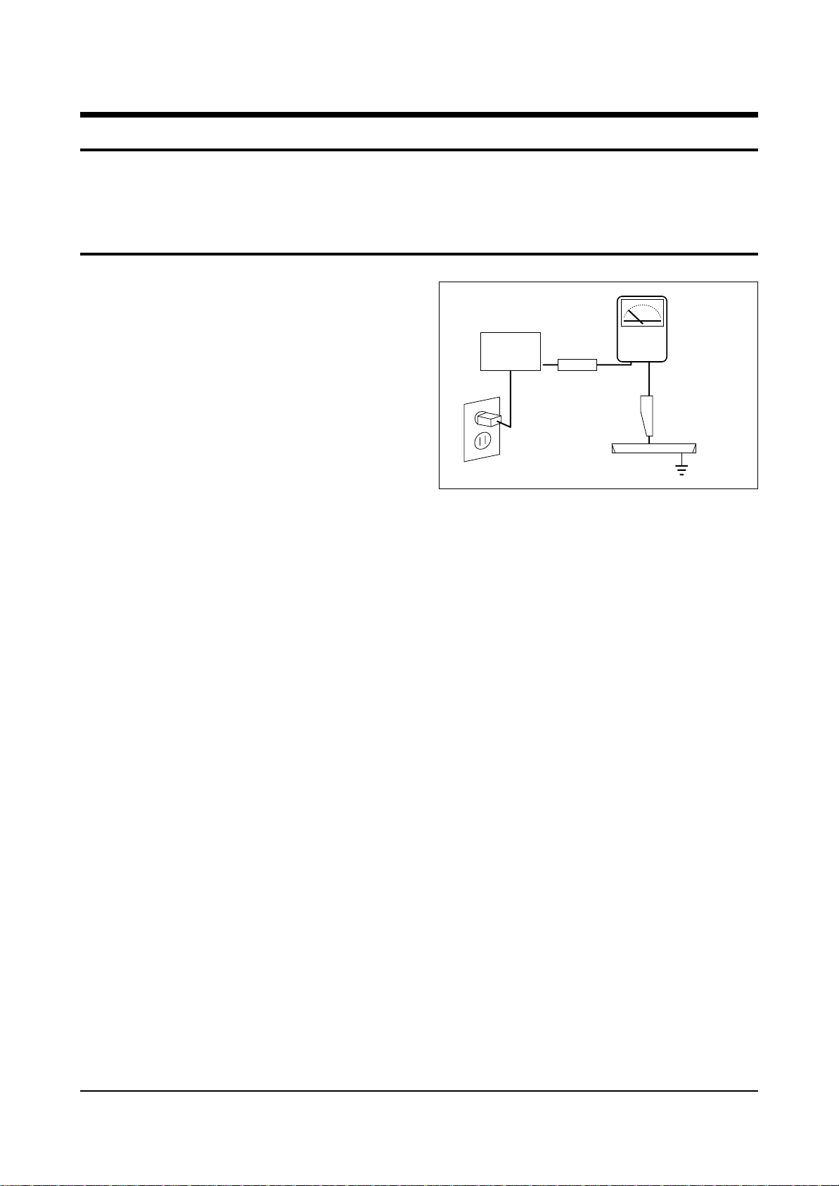
4. Leakage Current Hot Check (Figure 1-1):
Warning: Do not use an isolation
transformer during this test. Use a leakagecurrent tester or a metering system that
complies with American National Standards
Institute (ANSI C101.1, Leakage Current for
Appliances), and Underwriters Laboratories
(UL Publication UL1950.5.2).
5. With the unit completely reassembled, plug
the AC line cord directly into the power
outlet. With the unit’s AC switch first in the
ON position and then OFF, measure the
current between a known earth ground (metal
water pipe, conduit, etc.) and all exposed
metal parts, including: antennas, handle
brackets, metal cabinets, screwheads and
control shafts. The current measured should
not exceed 3.5 milliamp. Reverse the powerplug prongs in the AC outlet and repeat the
test.
Fig. 1-1 AC Leakage Test
6. Antenna Cold Check:
With the unit’s AC plug disconnected from the
AC source, connect an electrical jumper across
the two AC prongs. Connect one lead of the
ohmmeter to an AC prong. Connect the other
lead to the coaxial connector.
Precautions
Samsung Electronics 1-1
LEAKAGE
CURRENT
TESTER
DEVICE
UNDER
TEST
TEST ALL
EXPOSED METAL
SURFACES
3-WIRE CORD
ALSO TEST WITH
PLUG REVERSED
(USING AC ADAPTER
PLUG AS REQUIRED)
EARTH
GROUND
(READING SHOULD
NOT BE ABOVE
3.5mA)
Follow these safety, servicing and ESD precautions to prevent damage and protect against potential
hazards such as electrical shock and X-rays.

1-2 Safety Precautions (Continued)
7. High voltage is maintained within specified
limits by close-tolerance, safety-related
components and adjustments. If the high
voltage exceeds the specified limits, check
each of the special components.
8. Design Alteration Warning:
Never alter or add to the mechanical or
electrical design of this unit. Example: Do not
add auxiliary audio or video connectors. Such
alterations might create a safety hazard. Also,
any design changes or additions will void the
manufacturer’s warranty.
9. Hot Chassis Warning:
Some TV receiver chassis are electrically
connected directly to one conductor of the AC
power cord. If an isolation transformer is not
used, these units may be safely serviced only
if the AC power plug is inserted so that the
chassis is connected to the ground side of the
AC source.
To confirm that the AC power plug is inserted
correctly, do the following: Using an AC
voltmeter, measure the voltage between the
chassis and a known earth ground. If the
reading is greater than 1.0V, remove the AC
power plug, reverse its polarity and reinsert.
Re-measure the voltage between the chassis
and ground.
10. Some TV chassis are designed to operate with
85 volts AC between chassis and ground,
regardless of the AC plug polarity. These units
can be safely serviced only if an isolation
transformer inserted between the receiver and
the power source.
11. Some TV chassis have a secondary ground
system in addition to the main chassis ground.
This secondary ground system is not
isolated from the AC power line. The two
ground systems are electrically separated by
insulating material that must not be defeated
or altered.
12. Components, parts and wiring that appear to
have overheated or that are otherwise
damaged should be replaced with parts that
meet the original specifications. Always
determine the cause of damage or overheating, and correct any potential hazards.
13. Observe the original lead dress, especially
near the following areas: Antenna wiring,
sharp edges, and especially the AC and high
voltage power supplies. Always inspect for
pinched, out-of-place, or frayed wiring. Do
not change the spacing between components
and the printed circuit board. Check the AC
power cord for damage. Make sure that leads
and components do not touch thermally hot
parts.
14. Product Safety Notice:
Some electrical and mechanical parts have
special safety-related characteristics which
might not be obvious from visual inspection.
These safety features and the protection they
give might be lost if the replacement component differs from the original—even if the
replacement is rated for higher voltage,
wattage, etc.
Components that are critical for safety are
indicated in the circuit diagram by shading,
( ) or ( ).
Use replacement components that have the
same ratings, especially for flame resistance
and dielectric strength specifications.
A replacement part that does not have the
same safety characteristics as the original
might create shock, fire or other hazards.
15. Littum battery replace warning:
Danger of explosion if battery is incorrectly
replaced, Replace only with the same or
eqivalent type.
Precautions
1-2 Samsung Electronics
“CAUTION, Double-pole/neutral fusing”
CAUTION
Danger of explosion if battery is incorrectly
replaced.
Replace only with the same or equivalent type
recommended by the manufacturer.
Dispose of used batteries according to the manufacturer’s instructions.

1-3 Servicing Precautions
1. Servicing precautions are printed on the
cabinet. Follow them.
2. Always unplug the unit’s AC power cord from
the AC power source before attempting to: (a)
Remove or reinstall any component or
assembly, (b) Disconnect an electrical plug or
connector, (c) Connect a test component in
parallel with an electrolytic capacitor.
3. Some components are raised above the printed
circuit board for safety. An insulation tube or
tape is sometimes used. The internal wiring is
sometimes clamped to prevent contact with
thermally hot components. Reinstall all such
elements to their original position.
4. After servicing, always check that the screws,
components and wiring have been correctly
reinstalled. Make sure that the portion around
the serviced part has not been damaged.
5. Check the insulation between the blades of the
AC plug and accessible conductive parts
(examples: metal panels, input terminals and
earphone jacks).
6. Never defeat any of the B+ voltage interlocks.
Do not apply AC power to the unit (or any of
its assemblies) unless all solid-state heat sinks
are correctly installed.
7. Always connect a test instrument’s ground
lead to the instrument chassis ground before
connecting the positive lead; always remove
the instrument’s ground lead last.
8. Plasma display panels have partial afterimages when a same picture continues to be displayed for a certain time. This happens due to
the degradation of brightness caused by a
scale-down effect.
To prevent such afterimages when displaying
a same picture for a certain time, be sure to
reduce the level of brightness and contrast.
ex) Contrast : 50 or 75, Brightness : 25
9. Plasma display is an array of pixels(cells).
Therefore, if at least 99.9% pixels keep normal,
the appropriate panel is judged as ‘approved
product.’ Even though some of pixels keep
luminescent or always light off, do not worry
because the panel is approved.
Precautions
Samsung Electronics 1-3
Warning 1 : First read the “Safety Precautions” section of this manual. If some unforeseen circumstance creates a
conflict between the servicing and safety precautions, always follow the safety precautions.
Warning 2 : An electrolytic capacitor installed with the wrong polarity might explode.

1-4 Precautions for Electrostatically Sensitive Devices (ESDs)
1. Some semiconductor (“solid state”) devices
are easily damaged by static electricity. Such
components are called Electrostatically
Sensitive Devices (ESDs); examples include
integrated circuits and some field-effect
transistors. The following techniques will
reduce the occurrence of component damage
caused by static electricity.
2. Immediately before handling any semicon
ductor components or assemblies, drain the
electrostatic charge from your body by
touching a known earth ground. Alternatively,
wear a discharging wrist-strap device. (Be
sure to remove it prior to applying power—
this is an electric shock precaution.)
3. After removing an ESD-equipped assembly,
place it on a conductive surface such as
aluminum foil to prevent accumulation of
electrostatic charge.
4. Do not use freon-propelled chemicals. These
can generate electrical charges that damage
ESDs.
5. Use only a grounded-tip soldering iron when
soldering or unsoldering ESDs.
6. Use only an anti-static solder removal device.
Many solder removal devices are not rated as
“anti-static”; these can accumulate sufficient
electrical charge to damage ESDs.
7. Do not remove a replacement ESD from its
protective package until you are ready to
install it. Most replacement ESDs are
packaged with leads that are electrically
shorted together by conductive foam,
aluminum foil or other conductive materials.
8. Immediately before removing the protective
material from the leads of a replacement ESD,
touch the protective material to the chassis or
circuit assembly into which the device will be
installed.
9. Minimize body motions when handling
unpackaged replacement ESDs. Motions such
as brushing clothes together, or lifting a foot
from a carpeted floor can generate enough
static electricity to damage an ESD.
Precautions
1-4 Samsung Electronics
CAUTION
These servicing instructions are for use by
qualified service personnel only.
To reduce the risk of electric shock do not
perform any servicing other than that contained
in the operating instructions unless you are
qualified to do so.

Specifications
Samsung Electronics 3-1
3. Specifications
MODEL
SCREEN SIZE
3-1 Display(PDP Monitor)
Display
Remote Control
Display
Remote Control
Front
Back
Power Supply
Power Consumption
Screen Size
Adjustment System
Dimensions
(mm/inch)
Terminal
In/Out
Terminals
HPL5025/PPM50H2
16:9
1208.5(W) x 89(D) x 724(H) mm/47.58(W) x 3.5(D) x 28.50(H) Inches
54(W) x 31.5(D) x 220(H)mm/2.13(W) x 1.24(D) x 8.66(H) Inches
42Kg/92.59Ibs
150g/0.33Ibs
POWER Button, SOURCE, MENU, VOLUME, SELECT, MUTE
Exrernal Speaker Out, RGB1In (mD-Sub 15pin), RGB2 In(BNC jack)
SD/HD Cpmponent Video In, VIDEO In, S-VHS In,
Audio In(Video, Component, PC), RC-2332C In,
RS-232C Out (PPM50H2 Only), AC 120V
AC120V 60Hz
540W
1106.5(H) x 622(V)/43.56 x 24.49
Electronic Function Adjustment

Specifications
3-2 Samsung Electronics
MENO
Exploded View and Parts List
Samsung Electronics 4-1
4. Exploded View and Parts List
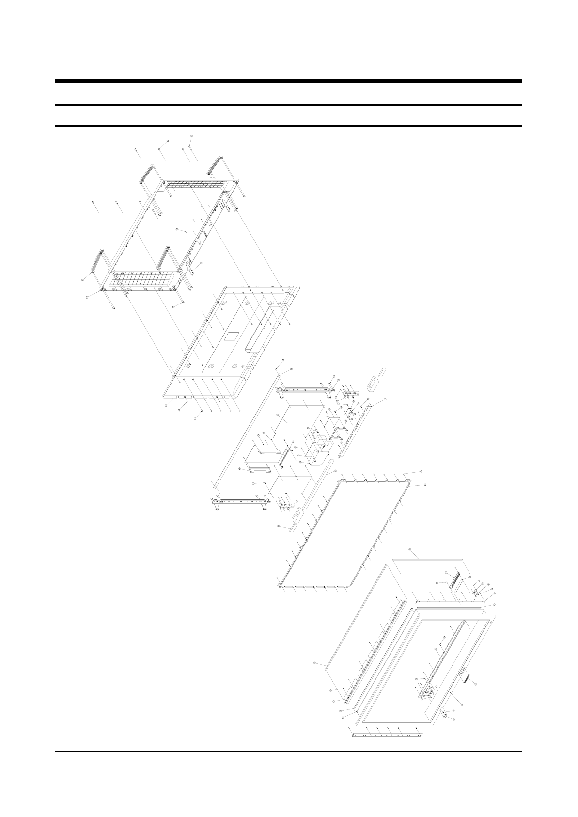
4-1 HPL5025X/XAA

Exploded View and Parts List
4-2 Samsung Electronics
NO PART DESCRIPTION CODE NO SPEC. Q’Ty REMARK
1 CABIN ET- FRONT AA64- 01548B HIPS V0 GRAY 1
2 BADGE - BRAND AA64- 01560B AL FORGING,SS 1
3 KNOB- MASTE R AA64-0 1566B ABS H B BLK 1
4 SPRING-CS AA61- 60003J SUS 304 1
5 BRACKET- F ILT ER,SIDE,ASSY AA61- 01004A 50P2 AL 6063 2
6 SCREW- T APTITE 6003-001020 RH,M4 *L10 YEL 12
7 ASSY- P CB,REMOCON AA95- 01208A D52A 1
8 SCREW- T APTITE 6003-001023 M3 * L 10 YEL 2
9 BRACKE T- FILT E R,BOT,ASS Y AA61- 01005A 50P2 AL 6063 1
10 SCREW- T APT ITE 6003- 001020 RH ,M4*L10 YEL 9
11 SCREW- ASSY,MACHINE 6006- 001035 WSP,PH,M3*L8YEL 2
12 ASSY- PCB,POWER ON/OFF AA95- 01211A HPL5025M,D52A 1
13 BRACKET - POWER AA61- 00716A SECC T 1 .0 1
14 SCREW- T APT ITE 6003- 001026 RH,+ ,B,M4 *L15 2
15 EMI- F ILTER AA95- 01207A HPL5025M,D52A 1
16 SPONGE- EMI,FILTER AA72- 00015A SHIELD-FORMT1 .2 2
17 BRACKET - FILTE R,T OP ,ASS Y AA61- 01003A 50P2 AL 6063 1
18 SCREW- T APT ITE 6003- 001020 RH ,M4*L10 YEL 7
19 SP ACER- FILTER AA60- 00110B P/U VO 2
20 ASS Y- P CB,CONTROL AA95- 01210A HPL5025M,D52A 1
21 KNOB- CON T ROL AA64- 01565B ABS HB BAK 1
22 SCREW- T APT ITE 6003- 001026 RH,+ ,B,M4 *L15 2
23 SPONGE- EMI,FILTER AA72- 00016A SHIELD-FORMT1 .2 2
24 SP ACER- FILTER AA60- 00110A P/U VO 2
25 ASSY- MODULE- 3 AA98- 00136A HPL5025M,D52A 1
26 SCREW- T APT ITE 6003- 001026 RH,+ ,B,M4 *L15 31
27 COVER- TERMINAL AA63- 00368B SUS T0 .5 1
28 SCREW- T APT ITE 6003- 001023 M3 * L10 YEL 4
29 B RAC K ET- E XTERNAL AA61- 00578B SPC T 1.0 1
30 ASSY- PCB,TERMINAL AA95- 01209A HPL5025M,D52A 1
31 SCREW- ASSY,MACHINE 6006- 001035 WSP,PH,M3*L8YEL 2
32 GU IDE- S TAND AA61- 00584B AL DIEC ASTIN G 2
33 SCREW- ASSY,MACHINE 6006- 001039 WSP,PH,M4*L12YEL 12
34 BRACKET - WALL AA61-00569A SECC T 2.0 2
35 SCREW- ASSY,MACHINE 6006- 001039 WSP,PH,M4*L12YEL 16
36 B RAC K ET- AV AA61- 00580B SPC T 1.0 1
37 ASSY- PCB,SOUND AA95- 00931A SPD- 50P2HM,D52A 1
38 SCREW- ASSY,MACHINE 6006- 001035 WSP,PH,M3*L8YEL 4
39 BRACKET - LINE,F ILT ER AA61- 00582B SPC T1 .0 1
40 ASS Y- P CB,POWER,AC B’d AA95- 01212A HPL5025M,D52A 1

Samsung Electronics 4-3
Exploded View and Parts List
NO PART DESCRIPTION CODE N O SPEC. Q’Ty REMARK
41 SCREW- ASSY,MACHINE 6006-001035 WSP,PH,M3*L8YEL 10
42 BRACKET- NOISE,F ILT ER AA61- 00589B SUS T 0.5 1
43 BRACK ET- SCALE R, SU B AA61-0 0581B SPC T 0.5 1
44 SCREW- ASSY,MACHINE 6006-001035 WSP,PH,M3*L8YEL 6
45 ASSY- P CB,MAIN(OPT) AA94- 05542A HPL5025M,D52A 1
46 BRACK ET- SCALE R, MAIN AA61- 00573B SPC T 1 .0 2
47 SCREW- ASSY,MACHINE 6006-001035 WSP,PH,M3*L8YEL 6
48 BRACKET- F AN,BASE AA61- 005 79B SECC T 1.6 5
49 FAN
50 SCREW- ASSY,MACHINE 6006-001017 WSP,PH,M4*L35YEL 10
51 SCREW- ASSY,MACHINE 6006-001035 WSP,PH,M3*L8YEL 10
52 COVER- BACK AA63-00364B AL 3003- 0 T 1.2 1
53 SCREW- T APT IT E 6003- 001019 M4 * L12 YEL 19
54 SCREW- T APT IT E 6003- 001020 M4 * L10 YEL 10
55 SPACER- FAN AA60- 00109A P/U FORM V0 BLK 5
56 HOLDER- F AN AA61- 00597B ABS V0 BL K 5
57 COVER- F AN AA63- 00366B SUS T 0.5 5
58 SCREW- T APT IT E 6003- 001026 M4 * L15 YEL 24
59 CABINET - BACK AA64- 01550B HIP S V0 BLK 1
60 HANDLE- SET AA64- 01551B ABS HB BLK 4
61 COVER- S ET AA63- 00365B ABS H B BLK 2
62 SCREW- ASSY,MACHINE 6006-001035 WSP,PH,M3*L8YEL 6
63 SCREW- ASSY,MACHINE 6006-001017 WSP,PH,M4*L35YEL 2
64 SCREW- ASSY,MACHINE 6006-001112 WSP,PH,M8*L16YEL 6
65 WINDOW- REMOCON AA64- 01549B ACRYL VIOLET 2:1 1
66 ASSY- P CB,SMPS,MAIN AA9 8- 00149A HPL5025M,D52A 1
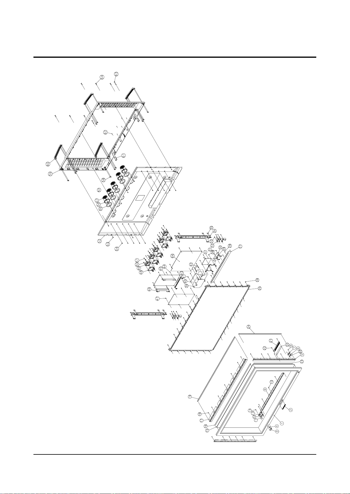
Exploded View and Parts List
4-4 Samsung Electronics
4-2 PPM50H2/XAA
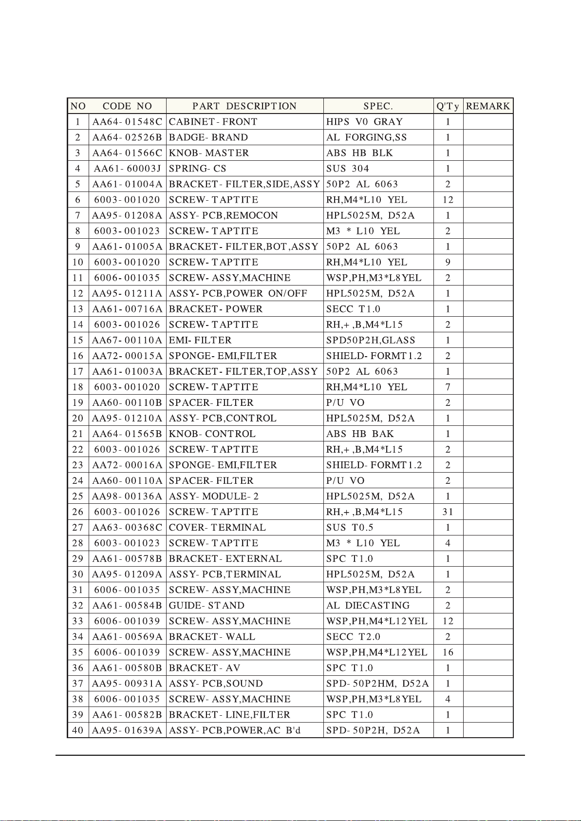
Samsung Electronics 4-5
Exploded View and Parts List

Exploded View and Parts List
4-6 Samsung Electronics

Alignment and Adjustments
Samsung Electronics 5-1
5. Alignment and Adjustments
5-1 Service Mode
5-1-1 SERVICE MODE ENTRY METHOD (General Transmitter)
1. Turn off the power to make the SET STAND-BY mode.
2. In order to enter the Service Mode, select MUTE-1-8-2-POWER.
Press the ‘Screen Display – Factory’ button when the system is turned on.
In case entry into SERVICE MODE is unsuccessful, repeat the procedures above.
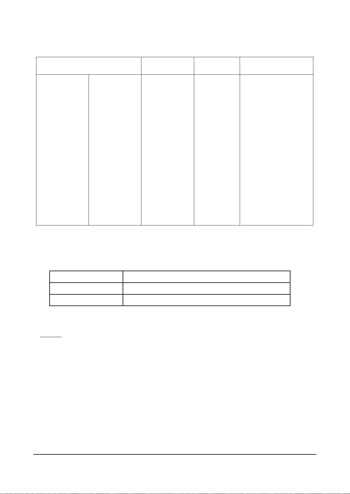
5-1-2 Initial DISPLAY State in times of SERVICE MODE Switch overs
PW364
INITIAL DISPLAY
SDA928 0 VP C3230 SDA9400
1, PW
364
2, SD
A928 0
3, V
PC3230
4, SD
A940 0
5, C
XA2101
6, A
D98 84
7, O
SD POSITION
8, O
PTION
9, R
ESET
10, A
GING
H
orizont alSize
V
er tical
Horizontal
Ve r t i c a l
Si
ze
Pos
Pos
CTIT
HRESH
CTIT
RAWID
Y- D
ELAY
L
PF GAIN
B
PF GAIN
H
PF GA IN
PH
ACOM
C
OR
B
RIGHT YUV
C
ONT YUV
I
FCOMP
ChromaB
and
L
uma LPF
H
PLL Speed
L
uma Delay
3230 Bri
ght
3230 C
ontr ast
HL
PF Y/C
L
PF Chroma
HHPeak Fil
ter
PeakingG
ain
C
oaring off / on
O
UT DELA Y
TNRCLY
CLY
TNRCLC
CLY
ST
OP MODE
Alignment and Adjustments
5-2 Samsung Electronics
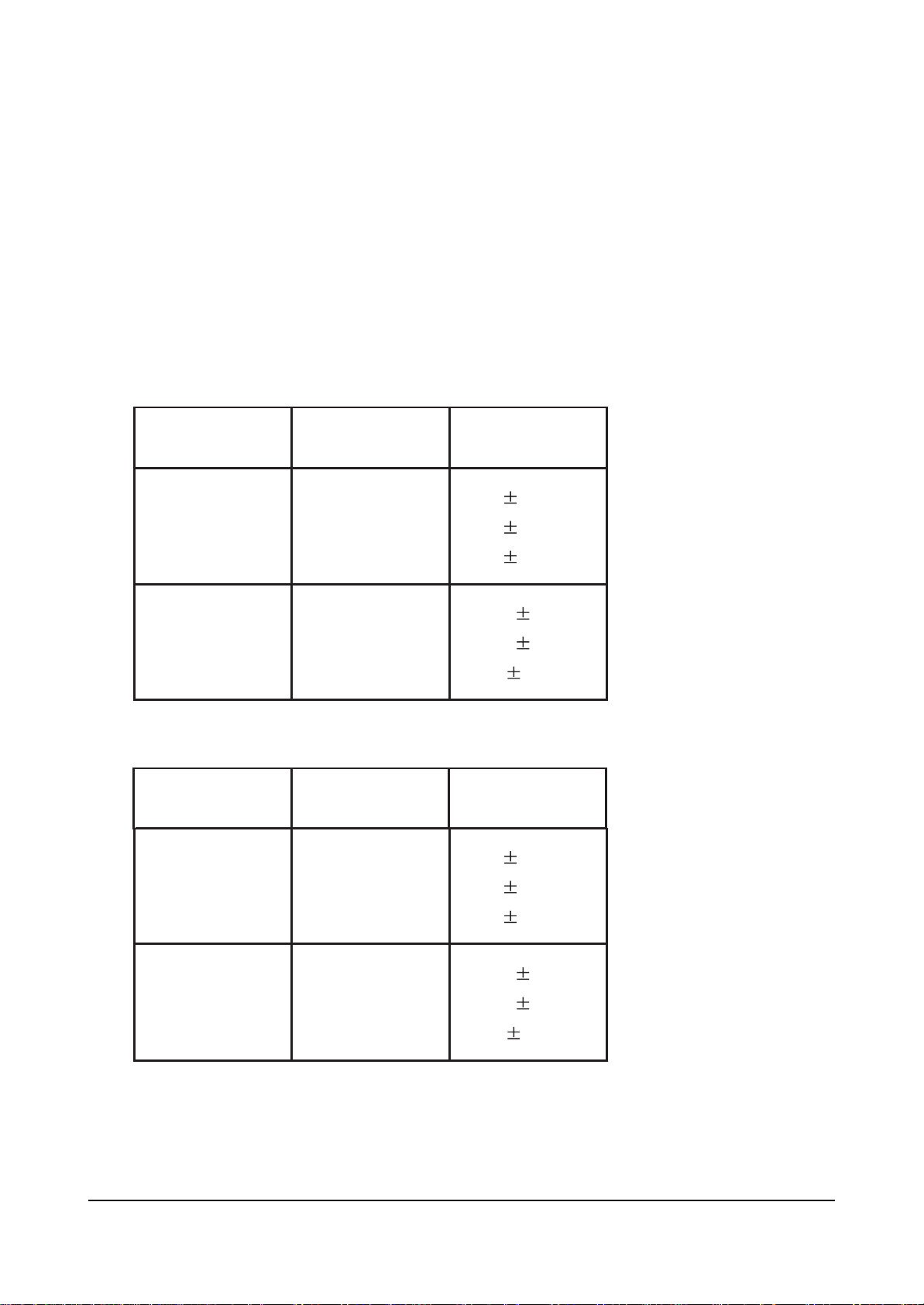
5-1-3 Buttons Operations within SERVICE MODE
#Notice
The existing service data may be deleted after downloading a program. Be sure to make a backup copy of
your data before downloading and then restore the data after completing the download.
Menu
Channel UP/DOWN
Volume UP/DOWN
Entire menu display
Cursor move to select items
Enable to increase and decrease the data of the selected items
Limit Level
Sys t em
D-Color
R-DRIVE
-DRIVE
G
-DRIVE
B
R-Cutoff
G-Cutoff
-C ut off
B
ABL MODE
ABL TH
HSEPSEL
CONT RAST
BRI GHT
CR OFFSET
CB
OFFSET1
CXA2101 AD9884
DRIVE
SUB BRI GHT
SUB CONT
SUB COLOR
SUB HUE
SUB SHP
R-Y/R
R-Y/B
GG-Y/R
-Y/B
P
ABL LEVEL
SHP FO
PRE/OVER
CTI LEVEL
1
LTI LEVEL
DC -T RAN
D-PIC
RED
Gain
GREEN
BLUE
OFFSET
RED
GREEN
BLUE
GAIN DRIVE
OFFSET DIRVE
V CONTRAST
V BRIGHT
PHASE
CHANGE PUMP
Gain
Gain
OFFSET
OFFSET
OSD
POSITION
HORIZ
VE RT
OP TION
1, BACK GROUND COLOR
SHIFT P IXEL
2,
PIXEL SHIFT
3,
PIXEL SHIFT
4,
FAN PROTECT
5,
TEMP
6,
7,
8, BASE LANGUAGE
PROTECT
SHARPNESS
MIN
SEC
Alignment and Adjustments
Samsung Electronics 5-3
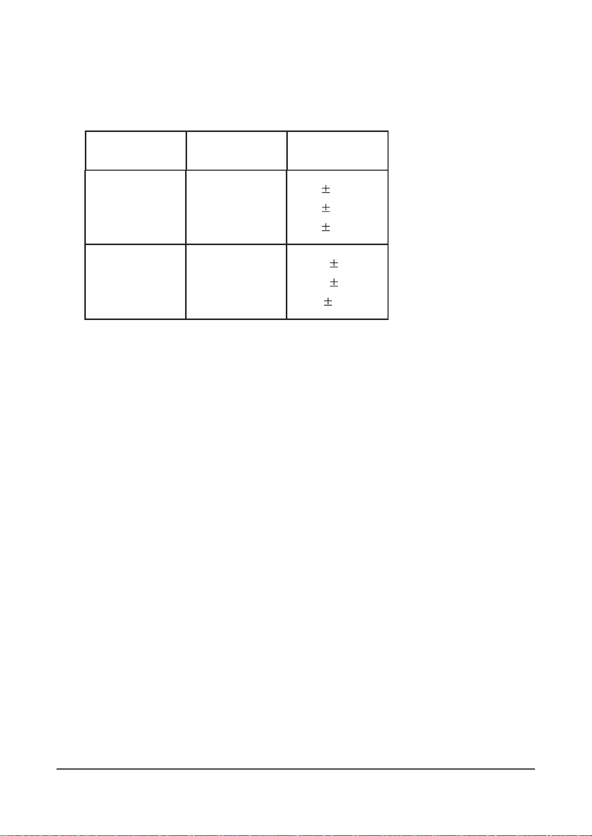
5-1-4 White Balance Adjust Method
1. Press MUTE-1-8-2-POWER to enter the factory mode.
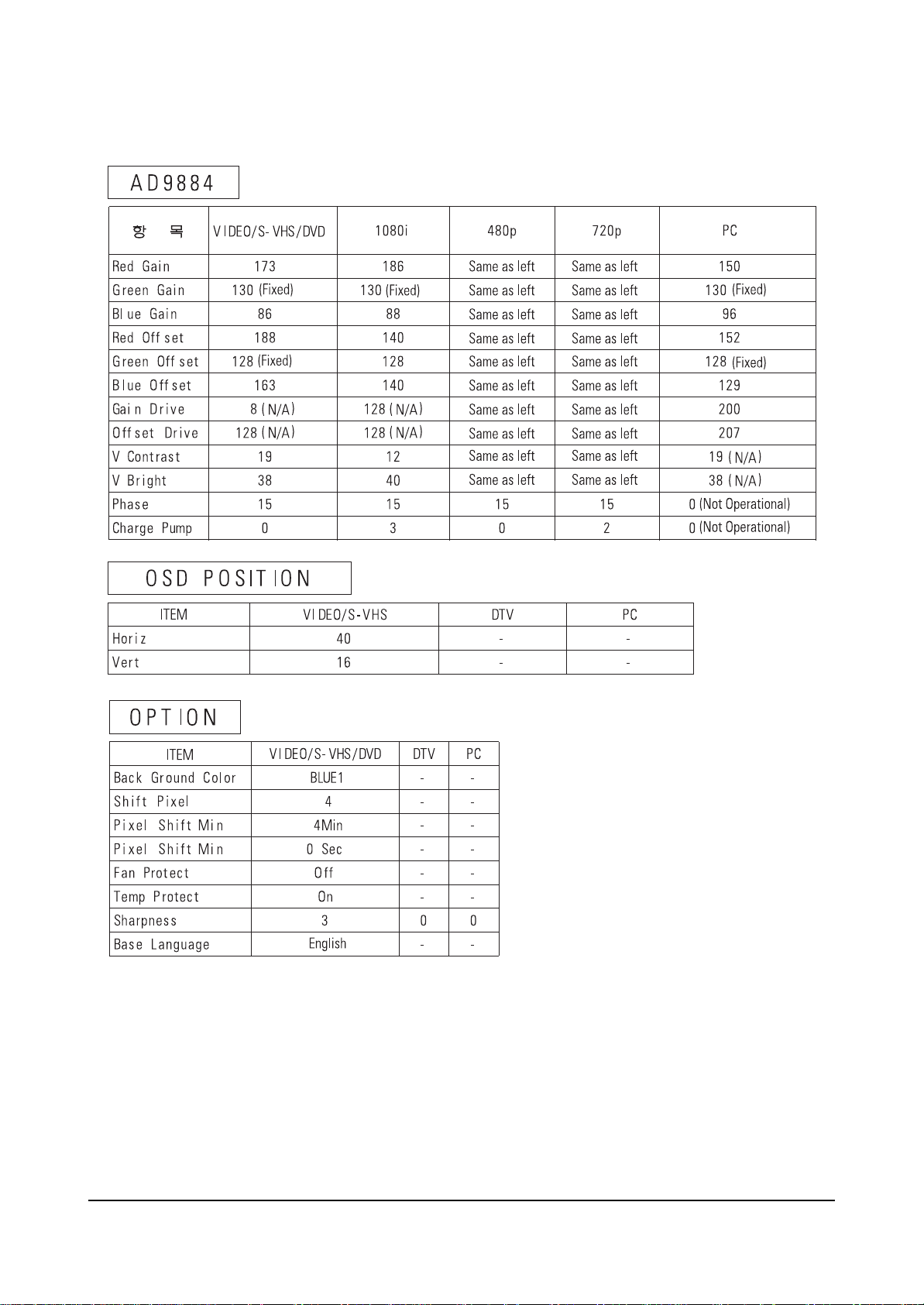
2. Enter AD9884
3. Adjust LOW coordinates as R, B OFFSET and HIGH coordinates as R, B GAIN.(GREEN is fixed.)
4. In AD9884, adjust brightness with V CONTRAST / V BRIGHT for VIDEO / DTV, and adjust with
GAIN DRIVE / OFFSET DRIVE for PC.
1. VIDEO MODE (SPR-3100, input TOSHIBA PATTERN)
2. DTV MODE (SPR-3100, input TOSHIBA PATTERN)
A
dj ustme
nt
Adjus tme
nt
Coor dinates
Coor dinates
Value
Deviation
A
dj ustme
nt
Adjus tme
nt
Coor dinates
Coor dinates
Value
Deviation
H
-LIGHT
-LIGHT
x:286
y
:
274
Y
:
18.7(fL)
3
3
3
L
H-LIGHT
-LIGHT
L
x:278
y
:
272
Y
:0.53(f L)
(f L)
5
5
0. 1
x:288
y
:
277
Y: 16.1
Y:
3
3
3
x:280
y
:277
0.71
5
5
0. 1
- W/B Adjustment SPEC (Suwom Factory Toshiba PATTERN)
Alignment and Adjustments
5-4 Samsung Electronics
2. PC MODE (VG828, input TOSHIBA PATTERN)
A
dj ustme
nt
Adjus tme
nt
Coor dinates
Coor dinates
Value
Deviation
H-LIGHT
-LIGHT
L
x:287
y:288
Y: 21.3(fL)
Y:
x:287
y:294
2.17
3
3
3
5
5
0. 1
Alignment and Adjustments
Samsung Electronics 5-5
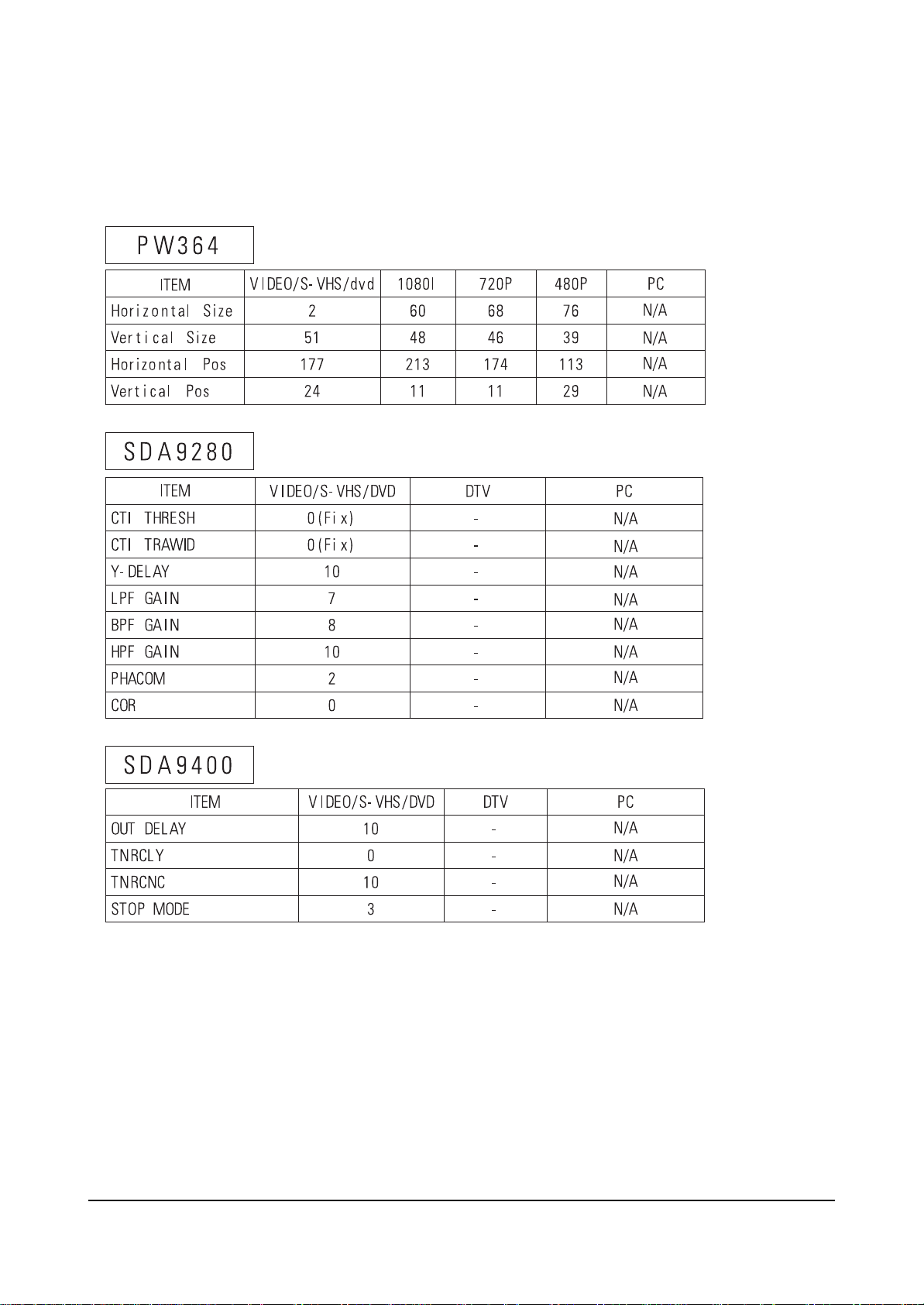
5-1-4 SCALAR FACTORY DATA DEFAULT VALUES

Alignment and Adjustments
5-6 Samsung Electronics
Alignment and Adjustments
Samsung Electronics 5-7

5-8 Samsung Electronics
Alignment and Adjustments
HPL5025/PPM50H2
VGA
1
2
3
4
5
6
7
8
9
10
11
12
13
14
Video signal Dot X Line
640 X 350
640 X 400
VGA
WVGA
720 X 400
640 X 480
848 X 480
Ve rtical
Frequency (Hz)
70.086
85.080
85.080
70.087
85.039
59.940
72.809
75.000
85.008
60.000
72.000
75.000
85.000
56.250
Horizontal
Frequency (kHz)
31.469
37.861
37.861
31.469
37.927
31.469
37.861
37.500
43.269
29.838
35.156
36.072
37.650
42.925
Ve rtical
polarity
N
N
P
P
P
N
N
N
N
P
P
P
P
N/P
Horizontal
polarity
P
P
N
N
N
N
N
N
N
N
N
N
N
N/P
15
16
17
18
19
20
21
22
23
24
25
26
27
SVGA
XGA
WXGA
SXGA
800 X 600
1024 X 768
1152 X 864
1280 X 768
1280 X 1024
60.317
72.188
75.000
85.061
60.004
70.069
75.029
84.997
75.000
60
75
60.020
75.025
37.879
48.077
46.875
53.674
48.363
56.476
60.023
68.677
67.500
47.700
60.150
63.981
79.976
P
P
P
P
N
N
P
P
P
P
P
P
P
P
P
P
P
N
N
P
P
P
N
N
P
P
Alignment and Adjustments
Samsung Electronics 5-9
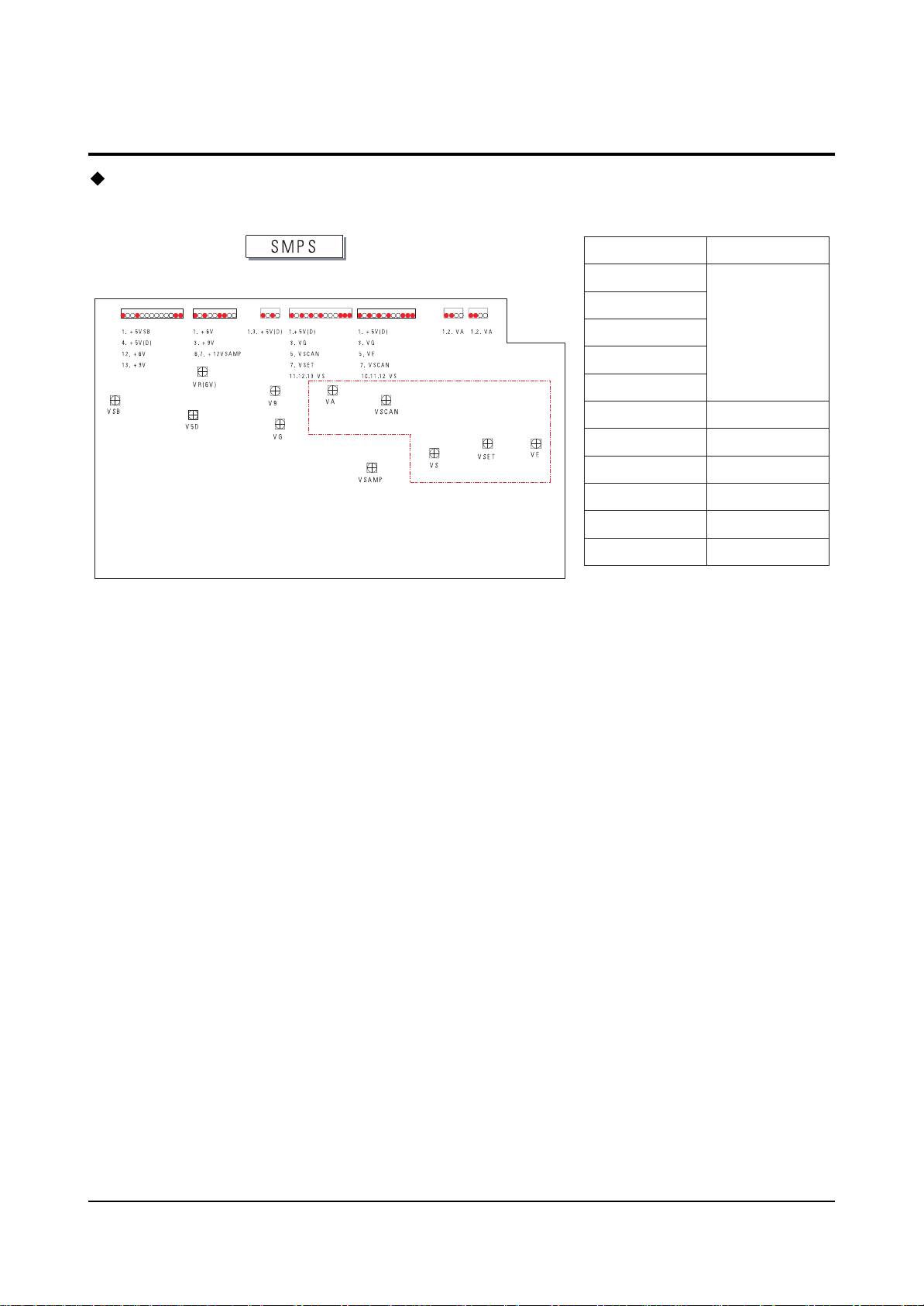
5-3 Adjusting the Discharge Voltage Of the Main Unit While Replacing ASS'Y (Body Part)
_ Turning the variable resistor clockwise reduces voltage except VG, V9, and VR(6).
OUTPUT
VE
VSET
VS
VSCAN
VA
VSAMP
VG
V9
V5D
VR(6)
VSB
Voltage(V)
See the labels
attached on the
base chassis
12
18.3
9
5.3
6
5.2
Alignment and Adjustments
5-10 Samsung Electronics
Alignment and Adjustments
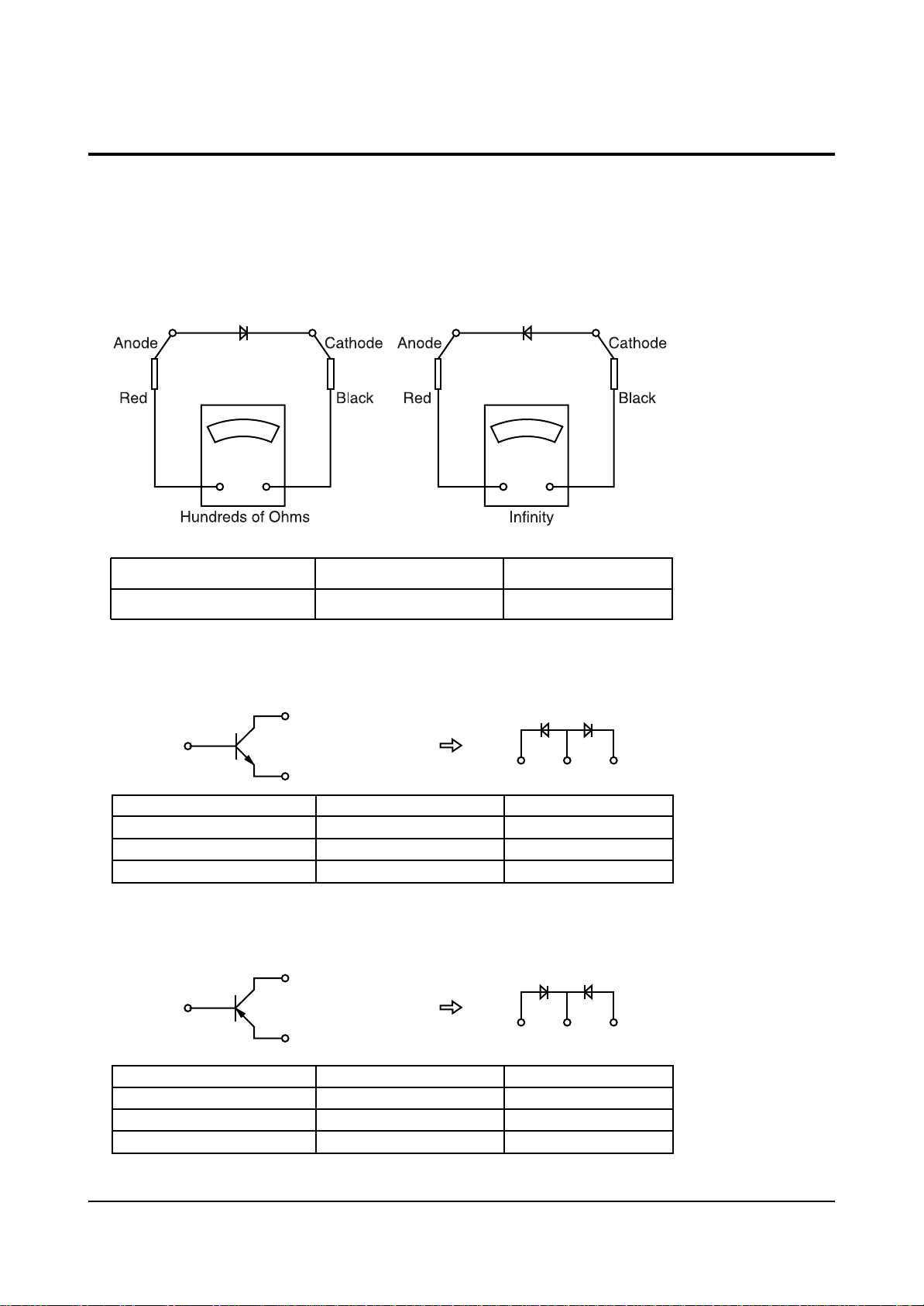
5-3 Fault Finding Using MULTI METER
Parts defects can be found for DIODE TRANSISTOR IC, using MULTI TEST including
Forward/Reverse direction Multi Test. Of course, in case resistance of several ohms and COIL are connected in parallel circuit, the lock out circuit parallel connected to part must be severed.
1.DIODE
2. TRANSISTOR
l For NPN(KSC815-Y, 2SC2068, 2SC2331-Y)
l For PNP(KSA539-Y)
Forward Direction
Hundreds of ohms
Reverse Direction
Infinity
Between Anode and Cathode
C (COLLECTOR)
E
B(BASE)
BC
C (COLLECTOR)
E
B(BASE)
BC
E (EMITTER)
E (EMITTER)
Forward Direction
Hundreds of ohms
Hundreds of ohms
Infinity
Reverse Direction
Infinity
Infinity
Infinity
Between B and E
Between B and C
Between E and C
Forward Direction
Hundreds of ohms
Hundreds of ohms
Infinity
Reverse Direction
Infinity
Infinity
Infinity
Between B and E
Between B and C
Between E and C
+- +-

Alignment and Adjustments
Samsung Electronics 5-11
Alignment and Adjustments
3. IC (INTEGRATED CIRCUIT)
IC has built in DIODE against overvoltage in PIN. Generally, except for internal circuit defects, IC defects
can be found, by measuring the DIODE.
- Defects have SHORT(0 ohm) for both forward and reverse direction.
Hundreds of ohms
Forward Direction
Reverse Direction
Varying depending on IC but generally normal
Infinity in DIODE TEST MODE

5-12 Samsung Electronics
MEMO

Circuit Operation Description
Samsung Electronics 6-1
6. Circuit Description
6-1 Power supply
6-1-1 Outline(PDP SMPS)
Considering various related conditions, the switching regulator with good efficiency and allowing for its
small size and light weight was used as the power supply for PDP 50inch, VS requiring high power consumption used forward converter and 12VSAMP used the simple flyback converter and other high voltage
(VSCAN,VSET,VE)used DC/DC converter. To comply with the international harmonics standards and
improve the power factor, active PFC(Power Factor Correction) was used to rectify AC input into +400V
DC output, which in turns used as input to the switching regulator.
6-1-2 50" SMPS Specification
(1) Input
The power supply shall be capable of supplying full rated output power over free voltage ranges that
are rated 100 VAC - 240 VAC RMS nominal. Operating voltage : 90 VAC - 264 VAC.
The power supply must be able to start up under peak loading at 90V AC. The power supply shall
automatically recover from AC power loss. (Note that nominal voltages for test purposes are considered
to be with +/- 1.0V of nominal).
+5VSB is a SELV standby voltage that is always present when AC mains voltage present.
(2) Output
This power supply is 13output switching power supply for PDP 50inch. The output voltage, and current
requirements for continuous operation are stated below. (Table1.)
Table1. Specifications of Output Power Supplies for PDP SMPS
Output Name Output Voltage Output Current(Max.) UsinginPDPDriving
Vsustain +160V ~ 200V (165V) 1.8A Sustain Voltage of Drive Board
Vaddress +58V ~ 73V (65V) 0.5A Address Voltage of Drive Board
Vscan +60V ~ 78V (70V) 0.05A
Vset +195V ~ 230V (215V) 0.05A
Ve +180V ~ 210V (185V) 0.05A
Vg +1V ~ 20V (18.4V) 0.3A Driving Voltage of Fet
Vfan +10V ~ 12V (11V) 0.8A Driving Voltage of Fan
V9 +1V ~ 10V (9.0V) 0.3A
V6 +1V ~ 8V (6.0V) 1.0A IC Driving Voltage of Logic Board
V5(D) +5.1V ~ 5.9V (5.4V) 3.5A
Vsb +4.8V ~ 5.4 V (5.2V) 0.4A Standby for Remote Control
V12 +10V ~ 12V (11V) 1.2A
Vsamp +10V ~ 13V (12V) 1.5A Amp Voltage of Audio Board

Circuit Operation Description
6-2 Samsung Electronics
(3) Over voltage Protection
The over voltage sense circuitry and reference shall reside in package that are separate and distinct from
the regulator control circuitry and reference. No single point fault shall be able to cause a sustained over
voltage condition on any of all outputs. The supply shall provide latch-mode Over Voltage Protection as
defined below. (Table2.)
Table2. Over voltage Protection.
(4) Short Circuit and Over current Protection.
An output short circuit is defined as output impedance of less than 300mohms. The power supply shall
shutdown and latch off for shorting VS DC rails to return or any other rail. Shorts between main output
rails and 5VSB shall not cause any damages to the power supply. The power supply shall either shutdown and latch off for shorting is removed, the P/S shall recover. The power supply shall be capable of
withstanding a continuous shot-circuit to the output without damage or over stress to the unit (components, PCB traces, connectors,etc.) under the input conditions specified in Section2 above.
Current Protection as defined below. (Table3.)
Table3. Over Current Protection.
Parameter Min Unit
VS(169V) 3.0 ~ A
VA(65V) 2.0 ~ A
5V(D) 10 ~ A
Parameter Min Unit
VS(169V) 195 ~ V
VA(65V) 90 ~ V
5V(D) 5.5 ~ V
Circuit Operation Description
Samsung Electronics 6-3
(5) Function of Board
REMOTE CONTROL
Using a 250V/10A relay, the board makes remote control available.
FREE VOLTAGE
The board is designed so that the input voltage can be used within 90VAC to 264VAC.
Improvement of power factor
The board is designed using the active PFC circuit so that the Power Factor can be over 9.0.
Protection
The OCP(Over current Protection), OVP(Over voltage Protection), Short Circuit Protection functions
are added against system malfunction.
(6) Part Block Diagram and Part Function.
AC-DC Converter
The Power supply output +400V DC from the common AC power supply using the active PFC
booster converter. This converter is designed for improving the power factor and preventing the
noise with high frequency and finally becomes the input power system for the switching regulator on
the output side.
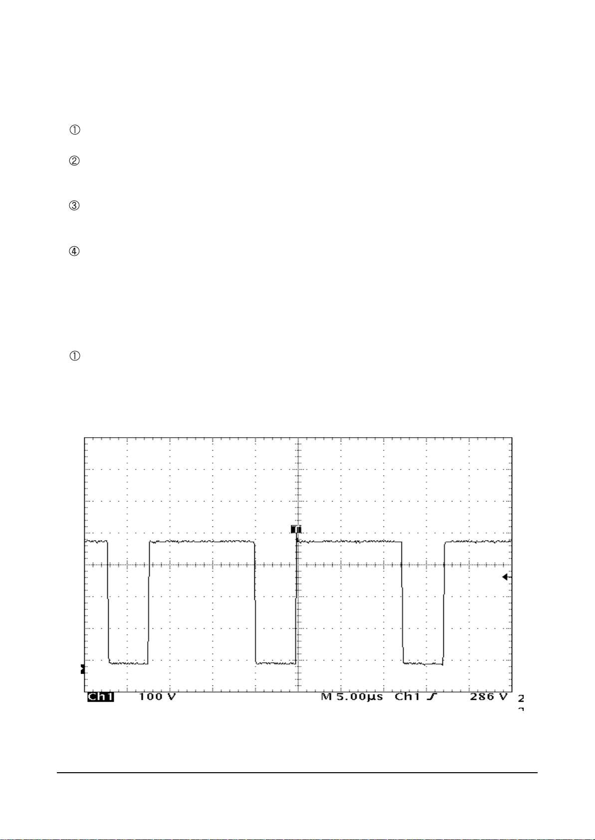
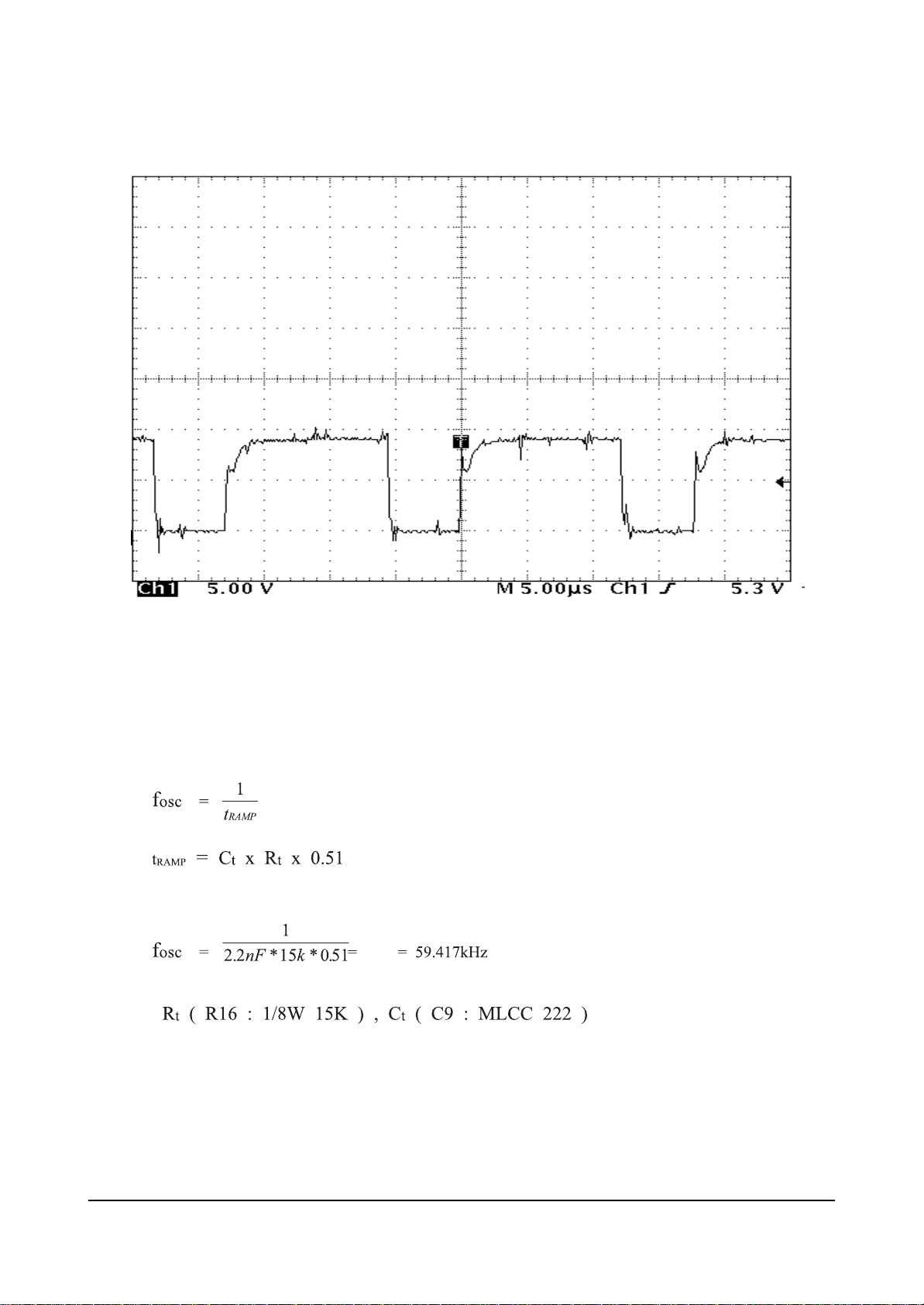
Picture1. PFC Drive FET(2SK2372) Drain pulse
Circuit Operation Description
6-4 Samsung Electronics
- Oscillator Frequency
Oscillator Frequency is determined by the values of Rt and Ct, which determine the ramp and
off-time of the oscillator output clock
Oscillator Frequency is derived from the following equation
For the circuit shown in the PDP50, with the oscillator running at
Picture2. PFC Drive FET(2SK2372) Gate pulse
 Loading...