Samsung gt-p6800 Service Manual
GSM TELEPHONE
GT-P6800
GSM TELEPHONE
CONTENTS
Safety Precautions
1.
Specification
2.
Product Function
3.
Exploded View and Parts list
4.
MAIN Electrical Parts List
5.
Level1Repair
6.
Level2Repair
7.
Level3Repair
8.
Reference data
9.
Notice: All functionality, features, specifications, and
other product information provided in this document,
including but not limited to, benefits, design, pricing,
components, performance, availability, and capabiliti
es of the product are subject to change without
notice. Samsung reserves the right to alter this doc
ument or the product described herein at anytime,
without obligation to provide notification of such
changes.

Safety Precautions
1.
Repair Precaution
1-1.
Before attempting any repair or detailed tuning, shield the device from RF noise or static
electricity discharges.
Use only demagnetized tools that are specifically designed for small electronic repairs,
as most electronic parts are sensitive to electromagnetic forces.
Use only high quality screwdrivers when servicing products. Low quality screwdrivers can
easily damage the heads of screws.
Use only conductor wire of the properly gauge and insulation for low resistance, because of
the low margin of error of most testing equipment.
We recommend
Hand-soldering is not recommended, because printed circuit boards(PCBs) can be easily
gauge twisted copper wire.
22-
damaged, even with relatively low heat. Never useasoldering iron withapower rating of
more than 100 watts and use only lead-free solder with a melting point below 250°C (482°F).
Prior to disassembling the battery charger for repair, ensure that the AC power is disconnected.
Always use the replacement parts that are registered in the SEC system. Third-party replac
ement parts may not function properly.
1-1
Confidential and proprietary-the contents in this service guide subject to change without prior notice.
Distribution, transmission, or infringement of any content or data from this document without Samsung’swritten authorization is strictly prohibited.

Safety Precautions
ESD(Electrostatically Sensitive Devices) Precaution
1-2.
Many semiconductors and ESDs in electronic devices are particularly sensitive to static discha
rge and can be easily damaged by it. We recommend protecting these components with cond
uctive anti-static bags when you store or transport them.
Always use an anti-static strap or wristband and remove electrostatic buildup or dissipate
static electricity from your body before repairing ESDs.
Ensure that soldering irons have AC adapter with ground wires and that the ground wires are
properly connected.
Use only desoldering tools with plastic tips to prevent static discharge.
Properly shield the work environment from accidental electrostatic discharge before opening
packages containing ESDs.
The potential for static electricity discharge may be increased in low humidity environments,
such as air-conditioned rooms. Increase the airflow to the working area to decrease the
chance of accidental static electricity discharges.
1-2
Confidential and proprietary-the contents in this service guide subject to change without prior notice.
Distribution, transmission, or infringement of any content or data from this document without Samsung’swritten authorization is strictly prohibited.

Specification
2.
GSM General Specification
2-1.
Freq.
Band[MHz]
Uplink/
Downlink
ARFCN
range
Tx/Rx
spacing
Mod. Bit
rate/
Bit Period
Time Slot
Period/
Frame
Period
GSM850 EGSM 900 DCS1800 PCS1900
824~849
869~894
128~251
45MHz 45MHz 95MHz 80MHz 190MHz 80MHz 45MHz 45MHz
270.833kbp
s
3.692us
576.9us
4.615ms
880~915
925~960
0~124 &
975~1023
270.833kbp
s
3.692us
576.9us
4.615ms
1710~1785
1805~1880
512~885 512~810
270.833kbp
s
3.692us
576.9us
4.615ms
1850~1910
1930~1990
270.833kbp
s
3.692us
576.9us
4.615ms
WCDMA
2100
1922~1977
2112~2167
UL:
9612~9888
DL:
10562~1083
8
3.84Mcps 3.84Mcps 3.84Mcps 3.84Mcps
FrameLengt
h:
10ms
Slotlength:
0.667ms
WCDMA
1900
1852~1907
1932~1987
UL:
9262~9538
DL:
9662~9938
FrameLengt
h:
10ms
Slotlength:
0.667ms
WCDMA
900
880~915
925~960
UL:
2712~2863
DL:
2937~3088
FrameLengt
h:
10ms
Slotlength:
0.667ms
WCMDA
824~849
869~894
4132~4233
4357~4458
FrameLengt
Slotlength:
0.667ms
850
UL:
DL:
h:
10ms
Modulation 0.3GMSK 0.3GMSK 0.3GMSK 0.3GMSK
MS Power
Power
Class
Sensitivity -102dBm -102dBm -100dBm -100dBm -106.7dBm -106.7dBm -106.7dBm -106.7dBm
TDMA Mux 8 8 8 8
Cell Radius 35Km 35Km 2Km 2Km 2Km 2Km 2Km 2Km
33dBm~5dBm33dBm~5dBm30dBm~0dBm30dBm~0dBm24dBm~
5pcl ~
19pcl
pcl
5
~19
pcl0pcl
~15
pcl0pcl
~15
QPSKHQPSKQPSKHQPSKQPSKHQPS
pcl
-50dBm
max+24dB
3(
m)
8
24dBm~
-50dBm
max+24dB
3(
m)
888
24dBm~
-50dBm
max+24dB
3(
K
m)
QPSKHQPS
K
24dBm~
-50dBm
max+24dB
3(
m)
2-1
Confidential and proprietary-the contents in this service guide subject to change without prior notice.
Distribution, transmission, or infringement of any content or data from this document without Samsung’swritten authorization is strictly prohibited.

Specification
GSM Tx Power Class
2-2.
TX Power
control
level
533±2
631±2
729±2
827±2
925±2
10 23±2
11 21±2
12 19±2
GSM850
dBm
dBm
dBm
dBm
dBm
dBm
dBm
dBm
TX Power
control
EGSM900
level
533±2
631±2
729±2
827±2
925±2
10 23±2
11 21±2
12 19±2
dBm
dBm
dBm
dBm
dBm
dBm
dBm
dBm
TX Power
control
DCS1800
level
030±3
128±3
226±3
324±3
422±3
520±3
618±3
716±3
dBm
dBm
dBm
dBm
dBm
dBm
dBm
dBm
TX Power
control
PCS1900
level
030±3
128±3
226±3
324±3
422±3
520±3
618±3
716±3
dBm
dBm
dBm
dBm
dBm
dBm
dBm
dBm
13 17±2
14 15±2
15 13±2
16 11±3
17 9±3
18 7±3
19 5±3
dBm
dBm
dBm
dBm
dBm
dBm
dBm
13 17±2
14 15±2
15 13±2
16 11±3
17 9±3
18 7±3
19 5±3
dBm
dBm
dBm
dBm
dBm
dBm
dBm
814±3
912±4
10 10±4
11 8±4
12 6±4
13 4±4
14 2±5
15 0±5
dBm
dBm
dBm
dBm
dBm
dBm
dBm
dBm
814±3
912±4
10 10±4
11 8±4
12 6±4
13 4±4
14 2±5
15 0±5
dBm
dBm
dBm
dBm
dBm
dBm
dBm
dBm
2-2
Confidential and proprietary-the contents in this service guide subject to change without prior notice.
Distribution, transmission, or infringement of any content or data from this document without Samsung’swritten authorization is strictly prohibited.

Operation Instruction and Installation
3.
Main Function
Android OS: Honeycomb
•
HSPA+21Mbps/HSUPA
•
MP AF with LED Flash,
•3
•7.67
•
•
•
•
-1.2
-
-
WVGA Super AMOLED Plus(C-Type)
GPS/BT v3.0 USB v2.0/WiFi
Recording definition:
Sensors: Accelerometer, Electromagnetic, Gyro, Light, Proximity
Additional
GHz Dual Core CPU
Application store/Precise Motion UI
Seamless Sharing Experience.
:
720p /
Mbps
5.7
FF
2M
(802.11
Playback at
a/b/g/n)/OTG
resolution
720p
3-1
Confidential and proprietary-the contents in this service guide subject to change without prior notice.
Distribution, transmission, or infringement of any content or data from this document without Samsung’swritten authorization is strictly prohibited.
Exploded View and Parts List
4.
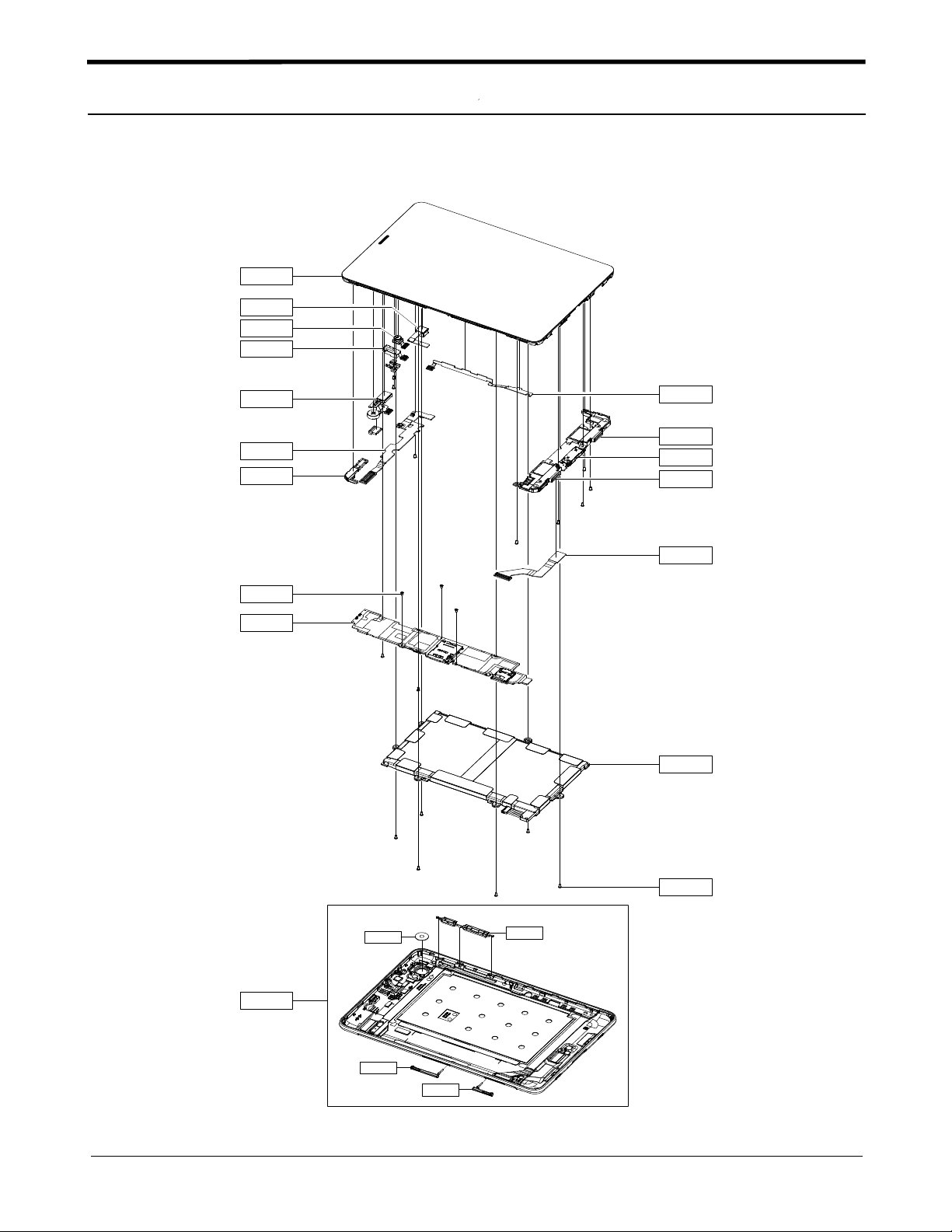
Cellular phone Exploded View
4-1.
QFR01
QCA01
QCA02
QJK01
QAR01
QME02
QAN02
QCR47
QMP01
QVK01
QSP02
QME15
QSP01
QME16
QBA01
QCR72
QCW01
QRE01
QRF06
QSD01
QVO01
4-1
Confidential and proprietary-the contents in this service guide subject to change without prior notice.
Distribution, transmission, or infringement of any content or data from this document without Samsung’swritten authorization is strictly prohibited.

Exploded View and Parts List
Cellular phone Parts list
4-2.
Design LOC Description SEC CODE
QCR47 SCREW-MACHINE
QCR72 SCREW-MACHINE
6001-001695
6001-002051
QAN02 INTENNA-GPS/WIFI(GT-P6800) GH42-03341A
QJK01 UNIT-EARJACK/FPCB ASSY GH59-11657A
QVK01 UNIT-VOL/PWR KEY PBA(GT-P6800) GH59-11660A
QME16 UNIT-CON TO CON(GT-P6800) GH59-11670A
QCA02 CAMERA MODULE-2M_LSI(GT-P6800) GH59-11684A
QME02 UNIT-SUB PBA(GT-P6800) GH59-11702A
QAR01 MODULE-RCV/MOT/SENSOR FPCB GH59-11706A
QSP01 MODULE-SPK/INTENNA_LEFT GH59-11756A
QSP02 MODULE-SPK/INTENNA_RIGHT(3G) GH59-11757A
QME15 UNIT-30PIN CON PBA(GT-P6800) GH59-11913A
QMP01 A/S ASSY-PBA MAIN(COMM) GH82-06191A
QCA01 ASSY CAMERA-3M
LSI MODULE(GT-P6800) GH96-05393A
1/5
QFR01 MEA FRONT-OCTA LCD ASSY(SVC) GH97-13092A
QRE01 ASSY CASE-REAR EU
SVC GH98-22345A
16G
QVO01 PMO WINDOW-CAMERA GH72-65664A
QSD01 PMO KEY-POWER VOLUME GH72-65665A
QRF06 PMO COVER-SIM GH72-65666A
QSD01 PMO COVER-SD GH72-65667A
4-2
Confidential and proprietary-the contents in this service guide subject to change without prior notice.
Distribution, transmission, or infringement of any content or data from this document without Samsung’swritten authorization is strictly prohibited.

MAIN Electrical Parts List
5.
SEC CODE Design LOC Description
0403-001688
0404-001250
0404-001361
0406-001241
0406-001375
0406-001413
0406-001413
0406-001413
0406-001413
0406-001413
0406-001413
0406-001459
0407-001002
0504-001113
0504-001138
0505-001325
0505-003052
0505-002720
0801-003024
0801-003031
0902-002847
1001-001481
1001-001700
1001-001715
1001-001733
1003-002216
1105-002212
1107-002086
1201-003308
1201-003317
1202-001121
1203-003307
1203-004776
1203-004818
1203-004819
1203-004925
D703,ZD500 DIODE-ZENER
D100,D101 DIODE-SCHOTTKY
D800 DIODE-SCHOTTKY
ZD703,ZD704 DIODE-TVS
ZD501 DIODE-TVS
ZD100,ZD300,ZD302 DIODE-TVS
ZD303,ZD700,ZD701 DIODE-TVS
ZD702,ZD705,ZD706 DIODE-TVS
ZD707,ZD708,ZD800 DIODE-TVS
ZD801,ZD802,ZD803 DIODE-TVS
ZD804 DIODE-TVS
D702 DIODE-TVS
D500 DIODE-ARRAY
Q100,Q400,TR700 TR-DIGITAL
TR800 TR-DIGITAL
TR504 FET-SILICON
TR503,U106 FET-SILICON
TR500,TR501,TR502 FET-SILICON
U300 IC
U403,U800 IC
UCP400 IC
U703 IC
U701 IC
U107 IC
U102 IC
U806,U808 IC
UME300 IC
UME400 IC
U200 IC
U103 IC
U700,U706 IC
U803 IC
U404 IC
U802,U809 IC
U401,U602,U907 IC
U804,U810 IC
5-1
Confidential and proprietary-the contents in this service guide subject to change without prior notice.
Distribution, transmission, or infringement of any content or data from this document without Samsung’swritten authorization is strictly prohibited.

Main Electrical Parts List
SEC CODE Design LOC Description
1203-005574
1203-006383
1203-006392
1203-006766
1203-006772
1203-006781
1203-006794
1203-006801
1203-006851
1203-006874
1203-006985
1203-007142
1205-004055
1205-004174
1205-004195
1205-004213
1205-004391
1205-004395
1205-004396
1209-002038
1209-002041
1209-002052
1404-001221
1405-001133
2007-000138
2007-000138
2007-000140
2007-000140
2007-000141
2007-000143
2007-000143
2007-000148
2007-000148
2007-000148
2007-000157
2007-000157
U904 IC
U801 IC
U501 IC
U705 IC
U108 IC
U502 IC
U704 IC
U104 IC
U500 IC
U204,U905 IC
U105 IC
U400 IC
U901 IC
U603 IC
U100 IC
UCP300 IC
U203 IC
U202 IC
U201 IC
U900 IC
U903 IC
U109,U902 IC
TH300,TH400 THERMISTOR-NTC
C1000,C199 VARISTOR
R801,R802,R811,R816 R-CHIP
R823,R824 R-CHIP
R456,R457,R472,R473 R-CHIP
R739,R740 R-CHIP
R825,R826 R-CHIP
R324,R325,R451,R452 R-CHIP
R517,R803 R-CHIP
R516,R725,R726,R727 R-CHIP
R728,R733,R742,R821 R-CHIP
R822 R-CHIP
R730,R734,R735,R736 R-CHIP
R737 R-CHIP
5-2
Confidential and proprietary-the contents in this service guide subject to change without prior notice.
Distribution, transmission, or infringement of any content or data from this document without Samsung’swritten authorization is strictly prohibited.

Main Electrical Parts List
SEC CODE Design LOC Description
2007-000159
2007-000162
2007-000162
2007-000166
2007-000167
2007-000170
2007-000172
2007-000173
2007-000242
2007-000758
2007-000758
2007-000775
2007-001284
2007-001288
2007-001306
2007-003010
2007-003015
2007-003029
2007-007092
2007-007107
2007-007107
2007-007132
2007-007137
2007-007139
2007-007156
2007-007310
2007-007312
2007-007334
2007-007517
2007-007517
2007-007528
2007-007573
2007-007766
2007-007861
2007-007942
2007-008043
R713,R714,R804 R-CHIP
R107,R515,R518 R-CHIP
R524,R529,R741,R902 R-CHIP
R715,R716 R-CHIP
R702 R-CHIP
R712,R810 R-CHIP
R806 R-CHIP
R828,R829 R-CHIP
R601 R-CHIP
R100,R108,R109,R528 R-CHIP
R532 R-CHIP
R101 R-CHIP
R304 R-CHIP
R718 R-CHIP
R521,R522,R523 R-CHIP
R924,R925 R-CHIP
R602,R603,R729,R731 R-CHIP
R412 R-CHIP
R732 R-CHIP
R308,R309,R413,R416 R-CHIP
R809 R-CHIP
R805 R-CHIP
R467 R-CHIP
R819 R-CHIP
R503,R504 R-CHIP
R211,R701,R807 R-CHIP
R478,R481 R-CHIP
R717 R-CHIP
R455,R458,R476,R477 R-CHIP
R911,R912,R913,R914 R-CHIP
R525 R-CHIP
R710 R-CHIP
R703 R-CHIP
R800 R-CHIP
R720,R724 R-CHIP
R105,R106 R-CHIP
5-3
Confidential and proprietary-the contents in this service guide subject to change without prior notice.
Distribution, transmission, or infringement of any content or data from this document without Samsung’swritten authorization is strictly prohibited.

Main Electrical Parts List
SEC CODE Design LOC Description
2007-008045
2007-008051
2007-008052
2007-008052
2007-008052
2007-008052
2007-008055
2007-008055
2007-008055
2007-008055
2007-008210
2007-008263
2007-008275
2007-008312
2007-008391
2007-008401
2007-008403
2007-008419
2007-008420
2007-008483
2007-008486
2007-008516
2007-008516
2007-008516
2007-008516
2007-008588
2007-008800
2007-008806
2007-009084
2007-009111
2007-009155
2007-009157
2007-009169
2007-009170
2007-009171
2007-009171
R104 R-CHIP
R203 R-CHIP
R310,R420,R421,R422 R-CHIP
R423,R470,R474,R475 R-CHIP
R814,R815,R901,R903 R-CHIP
R905 R-CHIP
R214,R318,R429,R432 R-CHIP
R433,R435,R436,R437 R-CHIP
R441,R443,R448,R449 R-CHIP
R450,R460,R483 R-CHIP
R704,R706 R-CHIP
R213 R-CHIP
R711 R-CHIP
R307 R-CHIP
R531 R-CHIP
R723 R-CHIP
R514,R808 R-CHIP
R453,R454 R-CHIP
R319,R479,R480 R-CHIP
R707,R708,R709 R-CHIP
R311 R-CHIP
R400,R402,R418,R419 R-CHIP
R425,R427,R468,R469 R-CHIP
R471,R482,R509,R510 R-CHIP
R512,R513 R-CHIP
R300,R301,R302,R827 R-CHIP
R459,R461 R-CHIP
R113,R700 R-CHIP
R722 R-CHIP
R411 R-CHIP
R320 R-CHIP
R462 R-CHIP
R511 R-CHIP
R442 R-CHIP
R403,R404,R405,R406 R-CHIP
R407,R408,R409,R410 R-CHIP
5-4
Confidential and proprietary-the contents in this service guide subject to change without prior notice.
Distribution, transmission, or infringement of any content or data from this document without Samsung’swritten authorization is strictly prohibited.

Main Electrical Parts List
SEC CODE Design LOC Description
2007-009314
2007-009408
2007-009794
2007-009801
2007-009804
2007-009805
2007-009866
2007-009879
2007-009964
2007-010029
2007-010233
2007-010856
2203-000138
2203-000233
2203-000233
2203-000254
2203-000278
2203-000386
2203-000438
2203-000489
2203-000627
2203-000725
2203-000812
2203-001153
2203-002443
2203-002687
2203-005138
2203-005682
2203-005683
2203-005725
2203-005726
2203-005726
2203-005729
2203-005731
2203-005736
2203-005789
R430 R-CHIP
R438,R439 R-CHIP
R207,R530 R-CHIP
R102,R103 R-CHIP
R600 R-CHIP
R208,R209 R-CHIP
R414 R-CHIP
R526 R-CHIP
R463,R466 R-CHIP
R465 R-CHIP
R313 R-CHIP
R527 R-CHIP
C808,C809 C-CERAMIC,CHIP
C102,C103,C183,C204 C-CERAMIC,CHIP
C206,C212,C261,L127 C-CERAMIC,CHIP
C100,C228,C570,C574 C-CERAMIC,CHIP
C230,C259,C260 C-CERAMIC,CHIP
C625 C-CERAMIC,CHIP
C235 C-CERAMIC,CHIP
C846,C847,C911 C-CERAMIC,CHIP
C227 C-CERAMIC,CHIP
C551 C-CERAMIC,CHIP
C341,C342,C343 C-CERAMIC,CHIP
C626 C-CERAMIC,CHIP
C800 C-CERAMIC,CHIP
C562,C566,C578 C-CERAMIC,CHIP
C455,C461 C-CERAMIC,CHIP
C111,C184,C200 C-CERAMIC,CHIP
C144 C-CERAMIC,CHIP
C338,C339,C457,C458 C-CERAMIC,CHIP
C110,C176,C185,C186 C-CERAMIC,CHIP
C189,C194 C-CERAMIC,CHIP
C253,C515,C523 C-CERAMIC,CHIP
C278 C-CERAMIC,CHIP
C143 C-CERAMIC,CHIP
C123,C134 C-CERAMIC,CHIP
5-5
Confidential and proprietary-the contents in this service guide subject to change without prior notice.
Distribution, transmission, or infringement of any content or data from this document without Samsung’swritten authorization is strictly prohibited.

Main Electrical Parts List
SEC CODE Design LOC Description
2203-005806
2203-006047
2203-006048
2203-006048
2203-006121
2203-006187
2203-006190
2203-006194
2203-006194
2203-006208
2203-006305
2203-006305
2203-006305
2203-006379
2203-006399
2203-006399
2203-006399
2203-006399
2203-006399
2203-006399
2203-006399
2203-006399
2203-006399
2203-006399
2203-006423
2203-006423
2203-006423
2203-006423
2203-006423
2203-006423
2203-006423
2203-006423
2203-006423
2203-006423
2203-006423
2203-006423
C121 C-CERAMIC,CHIP
C805 C-CERAMIC,CHIP
C101,C340,C462,C569 C-CERAMIC,CHIP
C571,C912 C-CERAMIC,CHIP
C245 C-CERAMIC,CHIP
C115 C-CERAMIC,CHIP
C446 C-CERAMIC,CHIP
C127,C148,C223,C303 C-CERAMIC,CHIP
C304 C-CERAMIC,CHIP
C525,C527,C528,C529 C-CERAMIC,CHIP
C219,C224,C225,C239 C-CERAMIC,CHIP
C251,C258,C266,C270 C-CERAMIC,CHIP
C274,C275,C276,C281 C-CERAMIC,CHIP
C116 C-CERAMIC,CHIP
C149,C165,C195,C196 C-CERAMIC,CHIP
C197,C198,C424,C453 C-CERAMIC,CHIP
C454,C501,C502,C532 C-CERAMIC,CHIP
C541,C565,C572,C575 C-CERAMIC,CHIP
C602,C603,C709,C810 C-CERAMIC,CHIP
C811,C812,C818,C823 C-CERAMIC,CHIP
C824,C827,C828,C829 C-CERAMIC,CHIP
C843,C845,C900,C901 C-CERAMIC,CHIP
C909,C910,C914,C915 C-CERAMIC,CHIP
C916 C-CERAMIC,CHIP
C125,C130,C135,C136 C-CERAMIC,CHIP
C137,C138,C139,C150 C-CERAMIC,CHIP
C151,C154,C155,C156 C-CERAMIC,CHIP
C158,C201,C202,C231 C-CERAMIC,CHIP
C233,C234,C236,C237 C-CERAMIC,CHIP
C242,C248,C284,C302 C-CERAMIC,CHIP
C305,C306,C316,C317 C-CERAMIC,CHIP
C318,C320,C321,C323 C-CERAMIC,CHIP
C324,C326,C327,C328 C-CERAMIC,CHIP
C331,C332,C333,C344 C-CERAMIC,CHIP
C400,C401,C402,C407 C-CERAMIC,CHIP
C412,C432,C436,C438 C-CERAMIC,CHIP
5-6
Confidential and proprietary-the contents in this service guide subject to change without prior notice.
Distribution, transmission, or infringement of any content or data from this document without Samsung’swritten authorization is strictly prohibited.

Main Electrical Parts List
SEC CODE Design LOC Description
2203-006423
2203-006423
2203-006423
2203-006462
2203-006474
2203-006562
2203-006642
2203-006647
2203-006647
2203-006648
2203-006665
2203-006668
2203-006815
2203-006824
2203-006839
2203-006839
2203-006872
2203-006872
2203-006872
2203-006872
2203-006872
2203-006872
2203-006872
2203-006872
2203-006872
2203-006872
2203-006890
2203-006896
2203-006979
2203-007147
2203-007194
2203-007210
2203-007210
2203-007210
2203-007230
2203-007240
C440,C442,C445,C456 C-CERAMIC,CHIP
C459,C460,C552,C608 C-CERAMIC,CHIP
C905,C906,C908,C913 C-CERAMIC,CHIP
C269,C277 C-CERAMIC,CHIP
C419,C420 C-CERAMIC,CHIP
C513,C710,C926 C-CERAMIC,CHIP
C431,C434 C-CERAMIC,CHIP
C140,C141,C142,C157 C-CERAMIC,CHIP
C616,C618 C-CERAMIC,CHIP
C129,C613,C614 C-CERAMIC,CHIP
C252,C280 C-CERAMIC,CHIP
C448,C449 C-CERAMIC,CHIP
C118,C122 C-CERAMIC,CHIP
C166 C-CERAMIC,CHIP
C131,C152,C255,C268 C-CERAMIC,CHIP
C512,C514,C606,C907 C-CERAMIC,CHIP
C153,C168,C203,C209 C-CERAMIC,CHIP
C214,C216,C232,C238 C-CERAMIC,CHIP
C241,C244,C246,C247 C-CERAMIC,CHIP
C250,C254,C403,C404 C-CERAMIC,CHIP
C406,C418,C426,C435 C-CERAMIC,CHIP
C437,C441,C535,C539 C-CERAMIC,CHIP
C540,C544,C545,C546 C-CERAMIC,CHIP
C615,C813,C815,C816 C-CERAMIC,CHIP
C817,C825,C826,C839 C-CERAMIC,CHIP
C840,C902,C903,C904 C-CERAMIC,CHIP
C524 C-CERAMIC,CHIP
C191,C192,C193 C-CERAMIC,CHIP
C106,C109,C620,C623 C-CERAMIC,CHIP
C443,C444,C463,C510 C-CERAMIC,CHIP
C240,C243,C279 C-CERAMIC,CHIP
C169,C300,C307,C312 C-CERAMIC,CHIP
C315,C319,C325,C329 C-CERAMIC,CHIP
C330,C334,C335,C345 C-CERAMIC,CHIP
C568 C-CERAMIC,CHIP
C336,C337,C452,C704 C-CERAMIC,CHIP
5-7
Confidential and proprietary-the contents in this service guide subject to change without prior notice.
Distribution, transmission, or infringement of any content or data from this document without Samsung’swritten authorization is strictly prohibited.

Main Electrical Parts List
SEC CODE Design LOC Description
2203-007271
2203-007271
2203-007271
2203-007317
2203-007317
2203-007317
2203-007317
2203-007317
2203-007317
2203-007317
2203-007317
2203-007342
2203-007391
2203-007393
2203-007393
2203-007449
2203-007449
2203-007449
2203-007449
2203-007449
2203-007449
2203-007449
2203-007449
2203-007449
2203-007449
2203-007449
2203-007449
2203-007449
2203-007456
2203-007474
2203-007474
2203-007474
2203-007474
2203-007474
2203-007474
2203-007775
C126,C215,C226,C267 C-CERAMIC,CHIP
C285,C286,C287,C439 C-CERAMIC,CHIP
C820 C-CERAMIC,CHIP
C128,C159,C164,C170 C-CERAMIC,CHIP
C171,C172,C405,C408 C-CERAMIC,CHIP
C413,C415,C421,C423 C-CERAMIC,CHIP
C505,C507,C508,C509 C-CERAMIC,CHIP
C516,C517,C518,C519 C-CERAMIC,CHIP
C520,C521,C522,C534 C-CERAMIC,CHIP
C538,C707,C830,C832 C-CERAMIC,CHIP
C834,C835 C-CERAMIC,CHIP
C806,C807 C-CERAMIC,CHIP
C249 C-CERAMIC,CHIP
C147,C451,C531,C821 C-CERAMIC,CHIP
C822 C-CERAMIC,CHIP
C167,C308,C309,C310 C-CERAMIC,CHIP
C322,C409,C410,C411 C-CERAMIC,CHIP
C414,C416,C417,C422 C-CERAMIC,CHIP
C425,C427,C428,C429 C-CERAMIC,CHIP
C430,C433,C464,C465 C-CERAMIC,CHIP
C500,C533,C536,C537 C-CERAMIC,CHIP
C542,C543,C547,C548 C-CERAMIC,CHIP
C549,C550,C607,C609 C-CERAMIC,CHIP
C610,C611,C617,C621 C-CERAMIC,CHIP
C622,C624,C701,C703 C-CERAMIC,CHIP
C831,C844,C917,C919 C-CERAMIC,CHIP
C920,C921,C922,C923 C-CERAMIC,CHIP
C927,C928 C-CERAMIC,CHIP
C503,C711 C-CERAMIC,CHIP
C161,C163,C311,C313 C-CERAMIC,CHIP
C314,C504,C506,C526 C-CERAMIC,CHIP
C553,C554,C555,C556 C-CERAMIC,CHIP
C557,C558,C559,C560 C-CERAMIC,CHIP
C561,C563,C564,C567 C-CERAMIC,CHIP
C708 C-CERAMIC,CHIP
C577 C-CERAMIC,CHIP
5-8
Confidential and proprietary-the contents in this service guide subject to change without prior notice.
Distribution, transmission, or infringement of any content or data from this document without Samsung’swritten authorization is strictly prohibited.

Main Electrical Parts List
SEC CODE Design LOC Description
2203-007781
2203-007795
2203-007795
2203-007795
2404-001561
2703-002176
2703-001729
2703-002207
2703-002208
2703-002313
2703-002314
2703-002369
2703-002596
2703-002649
2703-002858
2703-002901
2703-002907
2703-002999
2703-003546
2703-003686
2703-003755
2703-003869
2703-003892
2703-003908
2703-003909
2703-003911
2703-003917
2703-004000
2703-004014
2703-004018
2703-004033
2703-004034
2703-004037
2703-004037
2703-004185
2703-004189
C700 C-CERAMIC,CHIP
C301,C511,C576,C705 C-CERAMIC,CHIP
C712,C801,C802,C803 C-CERAMIC,CHIP
C804,C814 C-CERAMIC,CHIP
TA600 C-TA,CHIP
L208 INDUCTOR-SMD
L130 INDUCTOR-SMD
C263,L207 INDUCTOR-SMD
C265 INDUCTOR-SMD
L100,L202 INDUCTOR-SMD
L205 INDUCTOR-SMD
L206 INDUCTOR-SMD
L117,L120 INDUCTOR-SMD
L110 INDUCTOR-SMD
L111,L112 INDUCTOR-SMD
L122,L126 INDUCTOR-SMD
L125 INDUCTOR-SMD
L102 INDUCTOR-SMD
L400 INDUCTOR-SMD
L503 INDUCTOR-SMD
L116,L118,L119 INDUCTOR-SMD
L302,L303 INDUCTOR-SMD
L504 INDUCTOR-SMD
C208,L204 INDUCTOR-SMD
L501,L505 INDUCTOR-SMD
L500,L502,L700 INDUCTOR-SMD
L108,L132,L134 INDUCTOR-SMD
L105,L124,L129,L131 INDUCTOR-SMD
C177,C178,L113 INDUCTOR-SMD
L123,L128,C114 INDUCTOR-SMD
L203 INDUCTOR-SMD
C107,C108 INDUCTOR-SMD
C173,C174,C180,C181 INDUCTOR-SMD
L103,L104 INDUCTOR-SMD
L115 INDUCTOR-SMD
L801 INDUCTOR-SMD
5-9
Confidential and proprietary-the contents in this service guide subject to change without prior notice.
Distribution, transmission, or infringement of any content or data from this document without Samsung’swritten authorization is strictly prohibited.

Main Electrical Parts List
SEC CODE Design LOC Description
2703-004194
2801-004458
2801-004551
2801-004902
2801-004954
2801-005069
2809-001369
2809-001374
2901-001625
2901-001647
2904-001944
2904-001988
2904-002020
2904-002027
2910-000126
2911-000188
2911-000191
3301-001534
3301-001659
3301-001912
3301-001929
3301-001956
3301-002037
3301-002062
3301-002065
3705-001448
3705-001731
3709-001575
3709-001625
3711-006483
3711-006568
3711-006843
3711-007173
3711-007494
3712-001362
3712-001412
L506 INDUCTOR-SMD
OSC400 CRYSTAL-SMD
OSC300 CRYSTAL-SMD
OSC500 CRYSTAL-SMD
OSC202 CRYSTAL-SMD
OSC201 CRYSTAL-SMD
OSC100 CRYSTAL-SMD
OSC200 OSCILLATOR-VCTCXO
F800 FILTER-EMI/ESD
F801,F802 FILTER-EMI SMD
F202,F206 FILTER-SAW
F200 FILTER-SAW
F102 FILTER-SAW
F101 FILTER-SAW
F100 DUPLEXER-SAW
F205 DUPLEXER-FEM
U101 DUPLEXER-FEM
L900,L901,L902,L903 BEAD-SMD
L201 BEAD-SMD
L121 BEAD-SMD
L200,L600 BEAD-SMD
L300,L301 BEAD-SMD
L800 BEAD-SMD
L114 BEAD-SMD
L601,L602 BEAD-SMD
ANT100 CONNECTOR-COAXIAL
RFS100,RFS101 CONNECTOR-COAXIAL
CD700 CONNECTOR-CARD EDGE
CN300 CONNECTOR-CARD EDGE
HDC700 HEADER-BOARD TO BOARD
HDC800 HEADER-BOARD TO BOARD
HDC801 HEADER-BOARD TO BOARD
HDC300,HDC400 HEADER-BOARD TO BOARD
BAT500 CONNECTOR-HEADER
ANT101,ANT102 CONNECTOR-TERMINAL
ANT103,ANT104,ANT200 CONNECTOR-TERMINAL
5-10
Confidential and proprietary-the contents in this service guide subject to change without prior notice.
Distribution, transmission, or infringement of any content or data from this document without Samsung’swritten authorization is strictly prohibited.

Main Electrical Parts List
SEC CODE Design LOC Description
3712-001412
4709-001672
4709-002018
4709-002019
4709-002021
ANT201,ANT202 CONNECTOR-TERMINAL
F203 FREQ-DISTRIBUTER
F207 BALUN
F204 BALUN
F201 FREQ-DISTRIBUTER
GH80-03320A C207,R112,R115,R116 Solder Bridge PAD
GH80-03320A R117,R118,R119,R200 Solder Bridge PAD
GH80-03320A R201,R202,R204,R205 Solder Bridge PAD
GH80-03320A R206,R212,R216,R486 Solder Bridge PAD
GH80-03320A R487,R488,R813,R817 Solder Bridge PAD
GH80-03320A R900 Solder Bridge PAD
GH80-03321A R120,R210,R314,R315 Solder Bridge PAD
GH80-03321A R440,R719,R721,R904 Solder Bridge PAD
GH80-03321A R923 Solder Bridge PAD
GH98-21795A SC101 SHIELDCAN
GH98-21796A SC100 SHIELDCAN
5-11
Confidential and proprietary-the contents in this service guide subject to change without prior notice.
Distribution, transmission, or infringement of any content or data from this document without Samsung’swritten authorization is strictly prohibited.
Level
6.
S/W Download
6-1.
Repair
1
6-1-1.
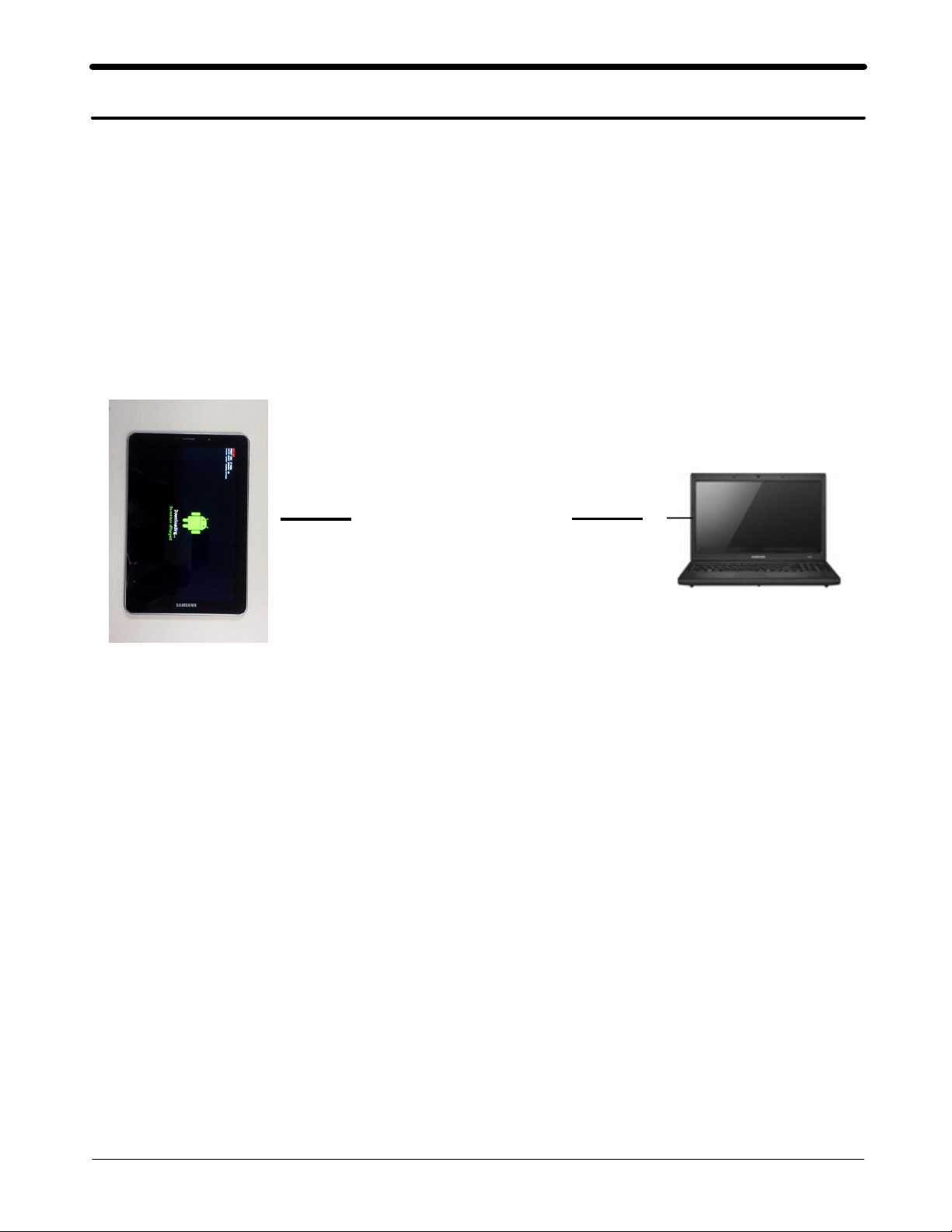
Pre-requisite for S/W Downloading
Downloader Program
y
GT-P6800 Tablet PC
y
Data Link Cable(GH39-01440B)
y
Binary files
y
Settings
(Odin3 v1.85.exe)
Data Link Cable
6-1
SAMSUNG Proprietary-Contents may change without notice
This Document can not be used without Samsung's authorization
Level1Repair
6-1-2.
S/W Downloader Program
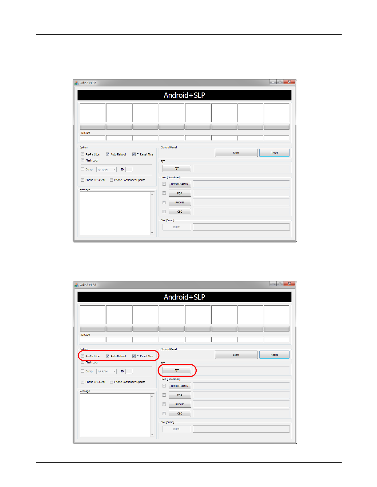
Load the binary download program by executing the
Odin3 v1.85.exe"
"
Å
Run this file.
Option Selection
.
1
Check Auto Reboot and F. Reset Time, then select PIT File
-
6-2
SAMSUNG Proprietary-Contents may change without notice
This Document can not be used without Samsung's authorization
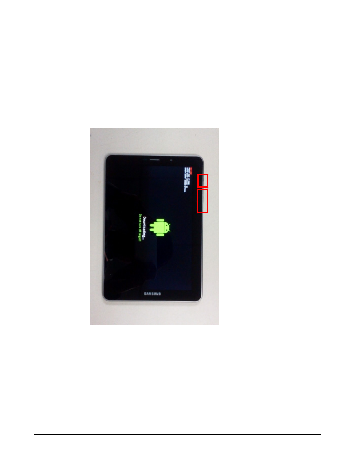
Enter Device into Download Mode
.
2
Press down on Volume Down button and power key at same time for
Press down on Volume Up button to enter device into download mode
-
ON / Off key
Level1Repair
seconds
10
Vol Up / Down key
6-3
SAMSUNG Proprietary-Contents may change without notice
This Document can not be used without Samsung's authorization
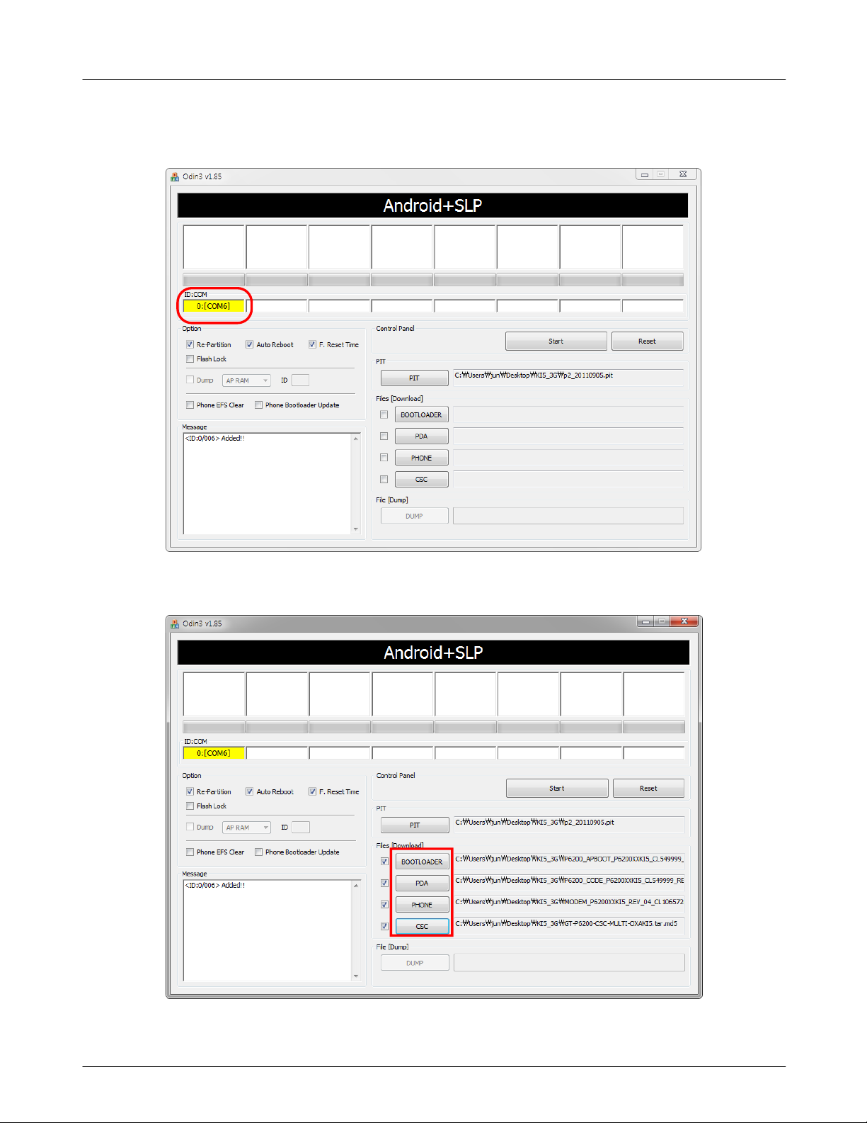
Level1Repair
Connect the Device to PC via Data Cable.
.
3
Make sure ID:COM box highlighted yellow that the device is connected to the PC.
Enable the check mark by click on the following options,
.
4
Check BOOTLOADER, PDA, PHONE, and CSC Files
-
6-4
SAMSUNG Proprietary-Contents may change without notice
This Document can not be used without Samsung's authorization

Level1Repair
Start downloading binary file into the device by clicking Start Button on the screen.
.
5
the green colored"PASS!" sign will appear on the upper-left box if the binary file
has been successfully downloaded into the device.
Disconnect the device from the Data cable.
6.
Once the device boots up,confirm the downloaded version name and etc.
.
7
*#1234#
Full Reset
:
*2767*3855#
:
6-5
SAMSUNG Proprietary-Contents may change without notice
This Document can not be used without Samsung's authorization
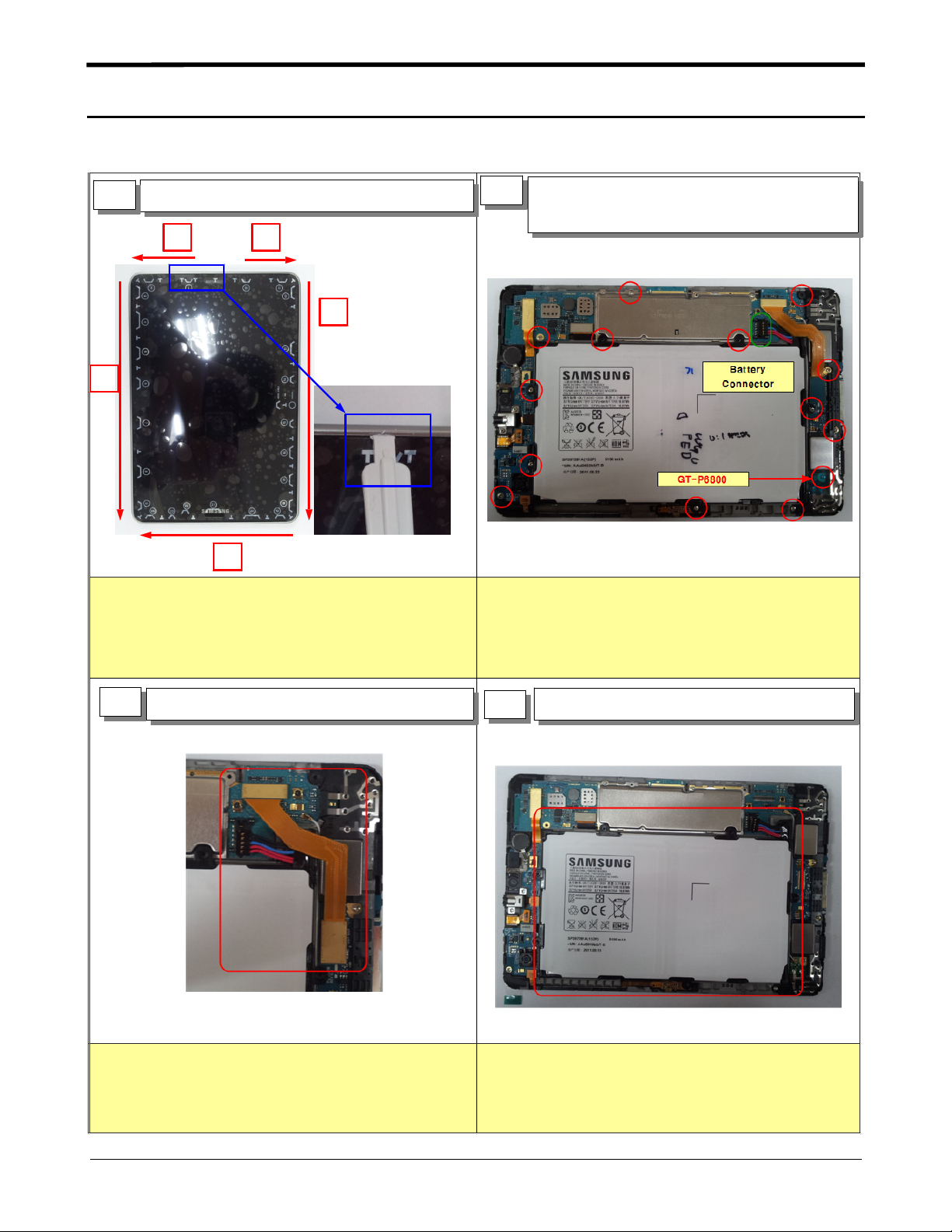
7.
7-1.
②
Level
Repair
2
Disassembly
1
Disassemble the Rear in order of the picture.
①
③
④
2
Loosen the13screws and then disassemble the
Battery Conncetor.
⑤
Be careful not to make scratch and molding damage!
1)
3
Disassemble the Connector FPCB(con to con)
Be careful not to makeascratch of FPCBs.
1)
Be careful not to make scratch and molding damage!
2)
Disassemble the Main Battery.
4
Be careful not to make scratch and molding damage!
1)
careful not to damage FPCBs
2) Be
Confidential and proprietary-the contents in this service guide subject to change without prior notice.
Distribution, transmission, or infringement of any content or data from this document without Samsung’swritten authorization is strictly prohibited.
Be careful not to make scratch and molding damage!
1)
7-1
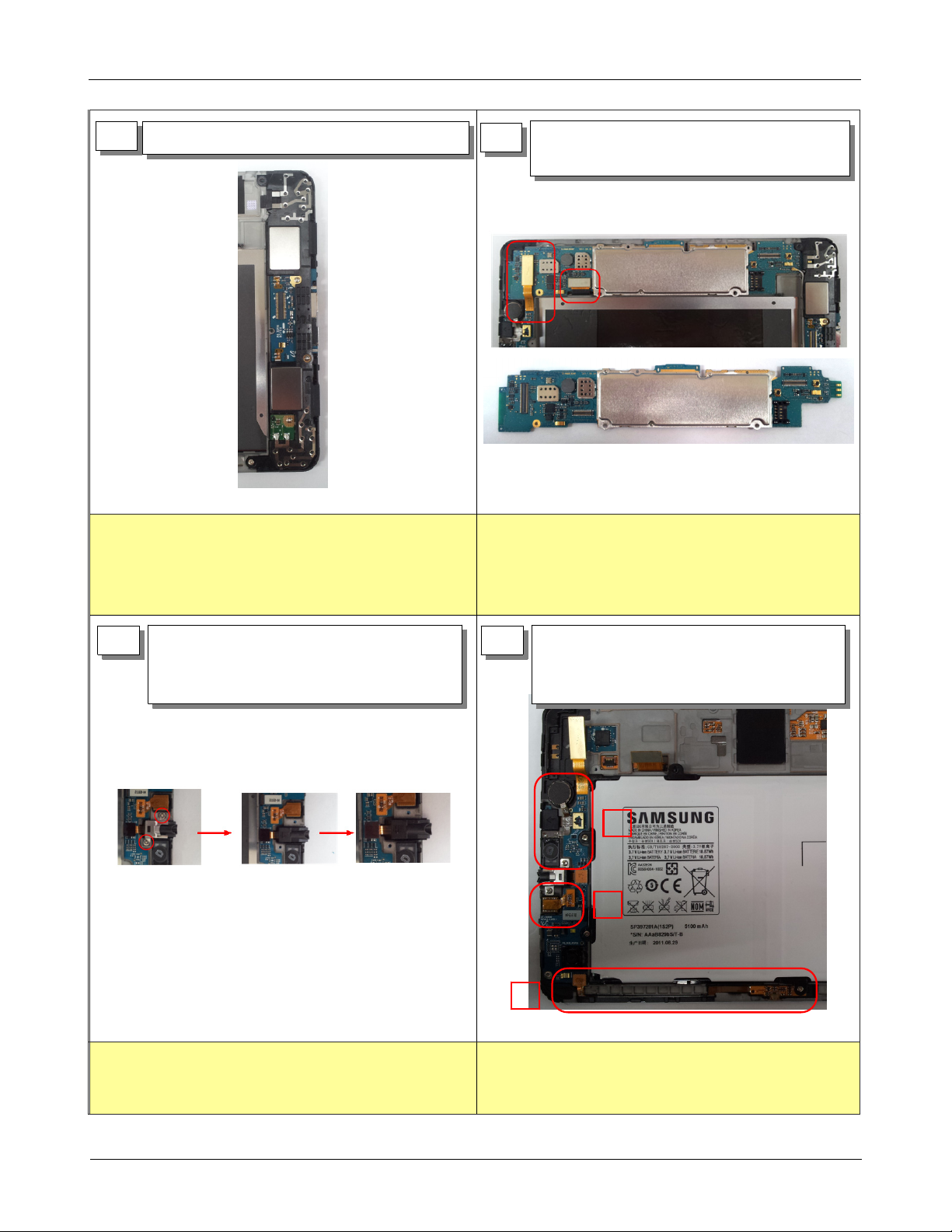
Level2Repair
7.
5
Disassemble the Speaker module.
Be careful not to make scratch and molding damage!
1)
Disassemble the Connector of OCTA, SUB
6
PBA and then disassemble MAIN PBA.
Be careful not to make scratch and molding damage!
1)
careful not to damage FPCB
2) Be
7
Disassemble Bracket of Earphone connector
after disassembling2screws and then lift the
Earphone connector.
Be careful not to make scratch and molding damage!
1)
8
Disassembly order refer to the picture.
VOLUME KEY FPCB
(
SENSOR RUBBER→SENSOR MODULE)
→
Mega CAMERA
2
→
③
②
①
Be careful not to make scratch and molding damage!
1)
careful not to damage FPCB
2) Be
7-2
Confidential and proprietary-the contents in this service guide subject to change without prior notice.
Distribution, transmission, or infringement of any content or data from this document without Samsung’swritten authorization is strictly prohibited.

Level2Repair
7.
9
Disassemble SUB PBA after disassembling
Mega Camera connector.
3
Be careful not to make scratch and molding damage!
1)
Be careful not to damage Receiver FPCB
3)
Disassemble WiFi antenna after disassembling
10
Mega Camera.
3
Be careful not to make scratch and molding damage!
1)
7-3
Confidential and proprietary-the contents in this service guide subject to change without prior notice.
Distribution, transmission, or infringement of any content or data from this document without Samsung’swritten authorization is strictly prohibited.
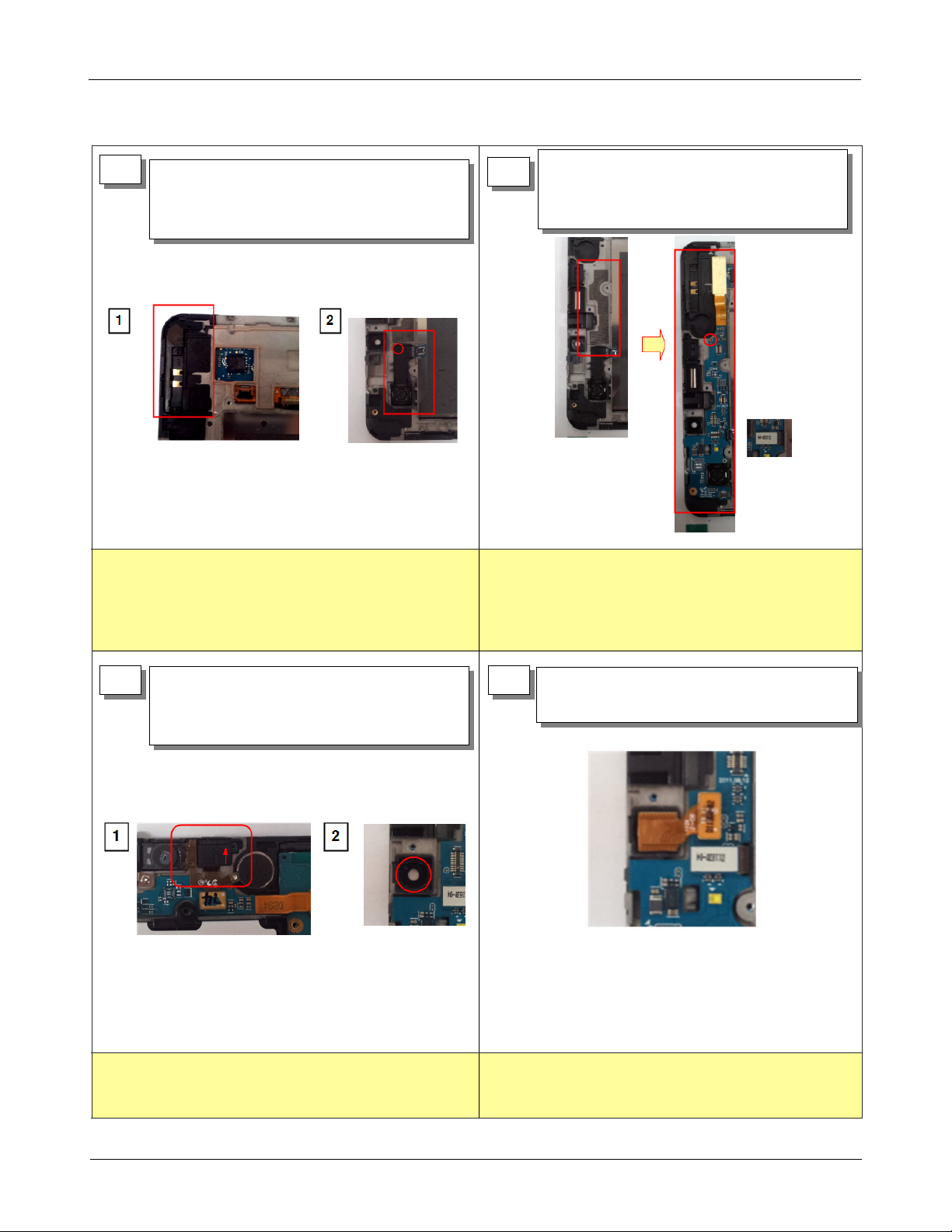
Level2Repair
7.
Assembly
7-2.
1
Place WIFI INTENNA and3Mega CAMERA on
OCTA
LCD Bracket Assembly.
Be careful not to make scratch and molding damage!
1)
Place the SUB PBA on the Bracket after
2
removing release paper and then assemble
the connector of3Mega CAMERA.
Be careful not to make scratch and molding damage!
1)
3 4
place the Camera Rubber after placing the
Sensor Rubber along the direction of the
below picture.
Be careful not to make scratch and molding damage!
1)
Place the2Mega CAMERA and then
assemble the Camera connector.
Be careful not to make scratch and molding damage!
1)
7-4
Confidential and proprietary-the contents in this service guide subject to change without prior notice.
Distribution, transmission, or infringement of any content or data from this document without Samsung’swritten authorization is strictly prohibited.

place the earphone connector bracket on LCD
5
Bracket after placing the earphone connector
as push to downside. And then screw the
screws.
Level2Repair
7.
6
place the Volume key FPCB on the LCD
2
Bracket follow the picture after removing
release paper of Volume Key FPCB. and
then assemble the Volume key FPCB
conncetor.
Be careful not to make scratch and molding damage!
1)
7
Attach the tapes in order of the below pictures.
Be careful not to make scratch and molding damage!
1)
8
Assemble the connectors(SUB PBA and OCTA
LCD) after placing the main PBA on LCD
Bracket.
Be careful not to make scratch and molding damage!
1)
Be careful not to make scratch and molding damage!
1)
7-5
Confidential and proprietary-the contents in this service guide subject to change without prior notice.
Distribution, transmission, or infringement of any content or data from this document without Samsung’swritten authorization is strictly prohibited.
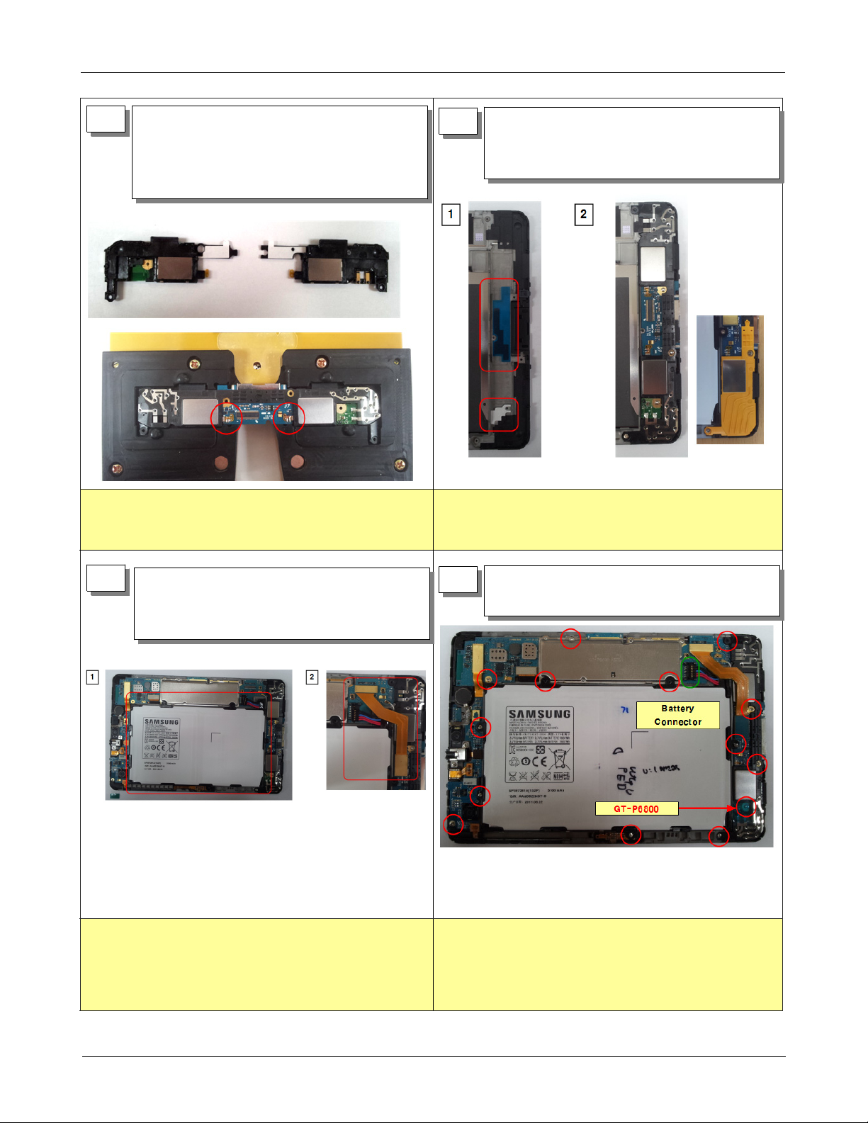
Level2Repair
7.
9
attach the Right and Left side speaker module
after removing the release paper of speaker
modules. and then solder the speaker modules
on the PCB of30pin IF connector.
10
Assemble speaker assembly module on LCD
Bracket after removing the release paper on
the LCD Bracket.
Be careful not to make scratch and molding damage!
1)
11
Assemble the connector main IF
FPCB(Connector to connector) after placing the
Battery.
Be careful not to make scratch and molding damage!
1)
12
Assemble the Battery connector after screwing
screws.
13
Be careful not to make scratch and molding damage!
1)
Be careful not to make scratch and molding damage!
1)
7-6
Confidential and proprietary-the contents in this service guide subject to change without prior notice.
Distribution, transmission, or infringement of any content or data from this document without Samsung’swritten authorization is strictly prohibited.
 Loading...