Level
8.
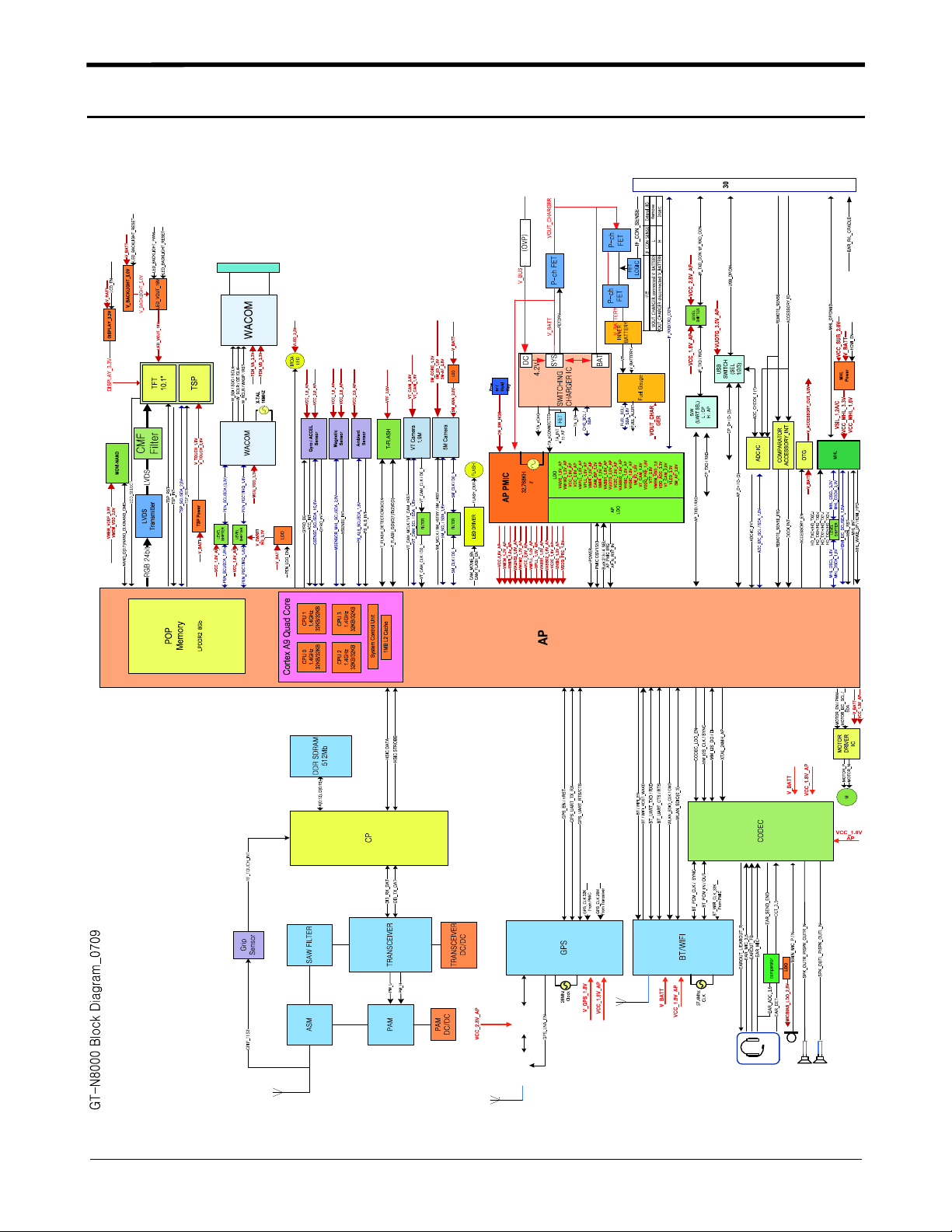
Block Diagram
8-1.
Repair
3
8-1
Confidential and proprietary-the contents in this service guide subject to change without prior notice.
Distribution, transmission, or infringement of any content or data from this document without Samsung’swritten authorization is strictly prohibited.
Level3Repair
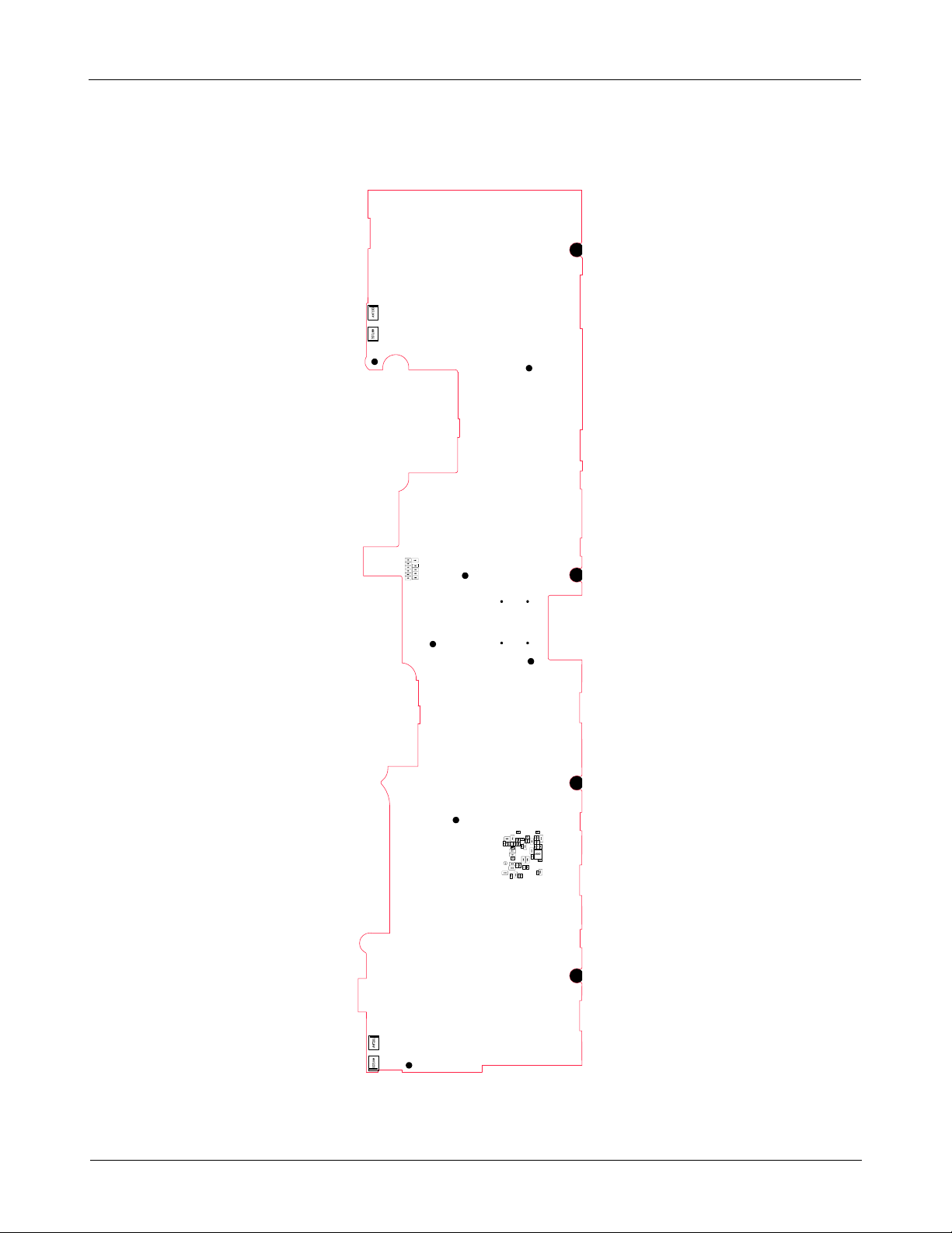
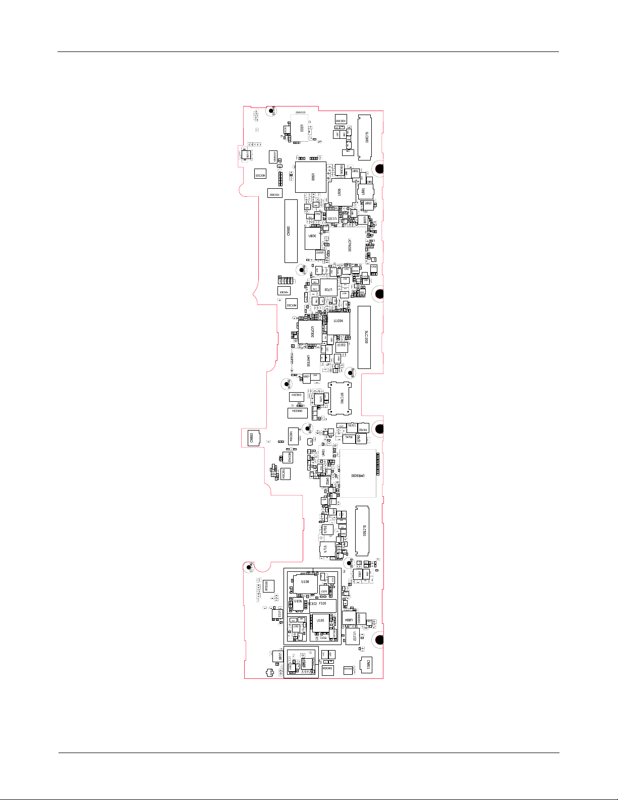
PCB Diagrams
8-2.
8-2-1.
Top
8-2
Confidential and proprietary-the contents in this service guide subject to change without prior notice.
Distribution, transmission, or infringement of any content or data from this document without Samsung’swritten authorization is strictly prohibited.
Level3Repair
8-2-2.
Bottom
8-3
Confidential and proprietary-the contents in this service guide subject to change without prior notice.
Distribution, transmission, or infringement of any content or data from this document without Samsung’swritten authorization is strictly prohibited.
Level3Repair
Flow Chart of Troubleshooting
8-3.
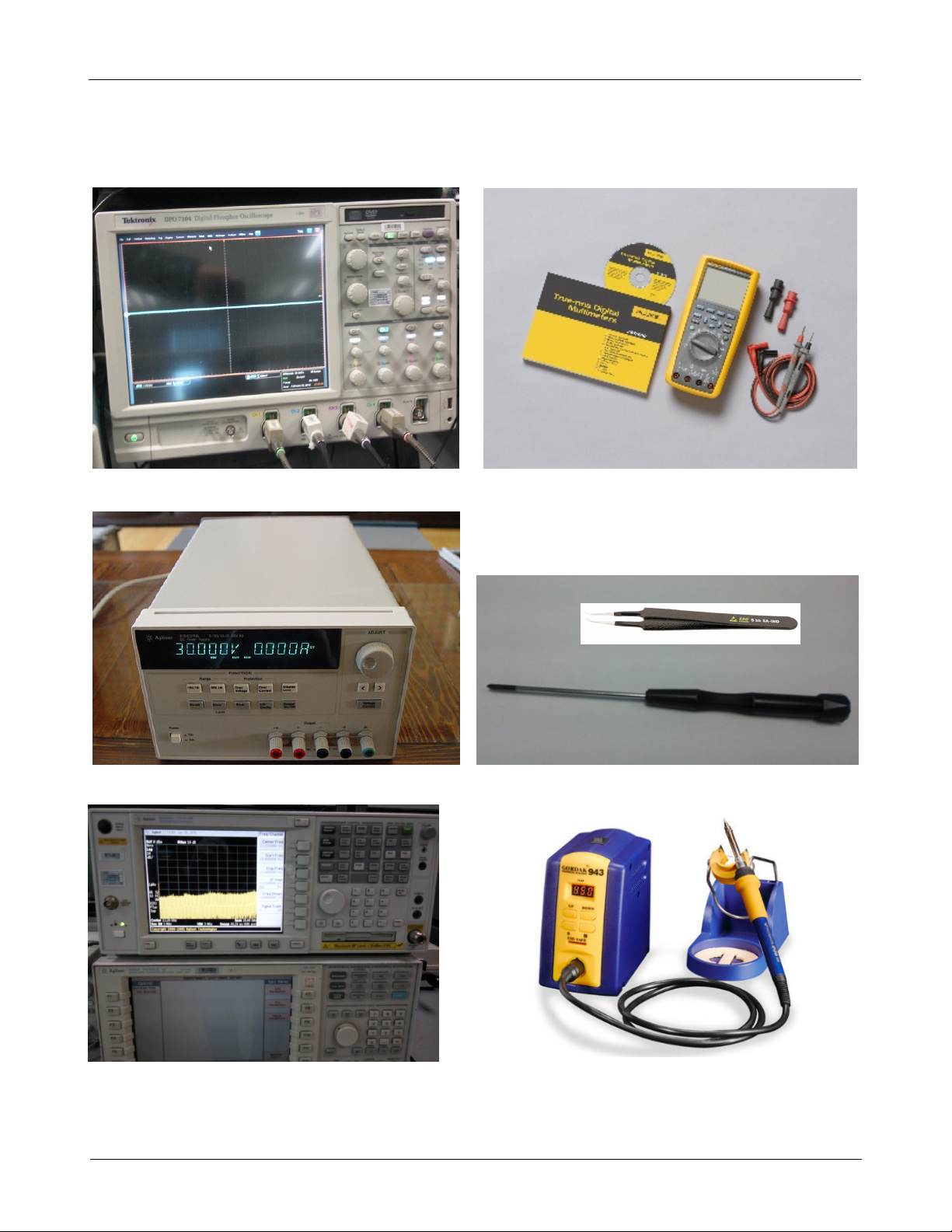
Equipments
Oscilloscope
Power Supply
Digital Multimeter
driver, ESD Safe Tweezer
+
8960 &
Confidential and proprietary-the contents in this service guide subject to change without prior notice.
Distribution, transmission, or infringement of any content or data from this document without Samsung’swritten authorization is strictly prohibited.
Spectrum Analyzer
8-4
Soldering iron
Level3Repair
8-3-1.
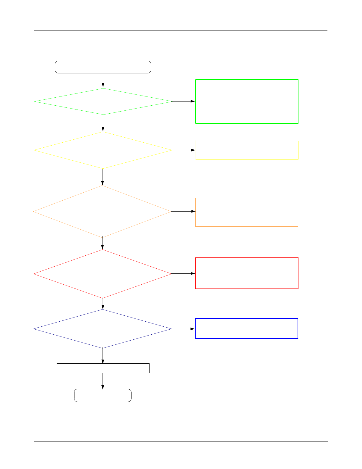
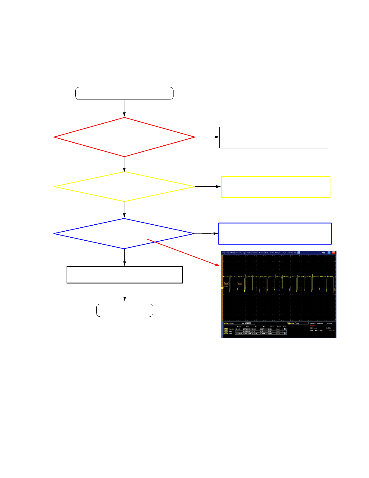
Power On
Power On'does not work
'
Check"Power on" by power
cablewithjig-on
Check the Battery Voltage
is more than
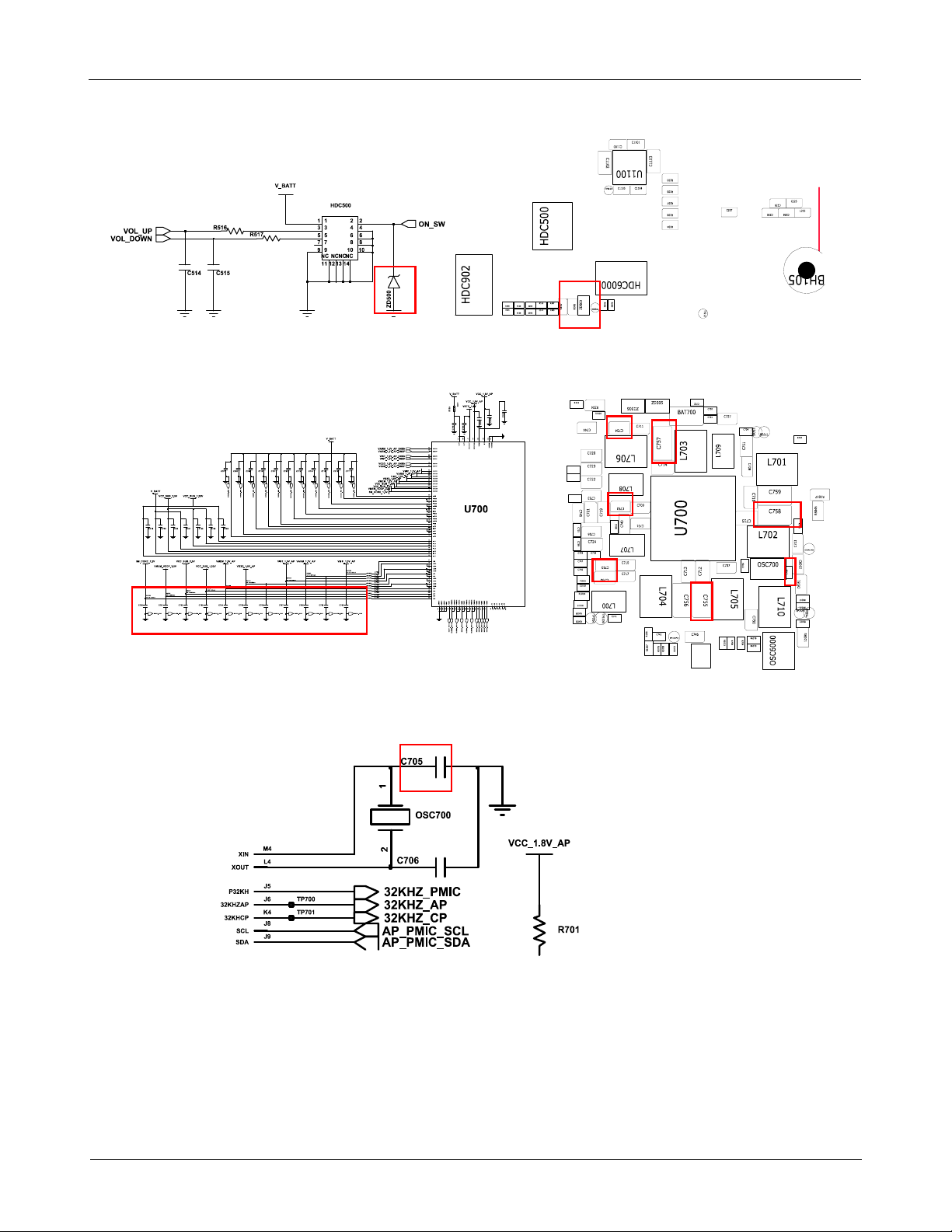
Check the ZD500
Voltage.(When you press the
power key, ZD500 Voltage
have to same V_BATT
Voltage)
Yes
Yes
Yes
3.5V
No
No
No
Check the30pin to50pin FPCB(SLC500),
Wrong assembly or Wrong connection.
Charge the Battery
Battery power is low
(
Change the power key FPCB
GH59-11713A)
(
Battery power is low
(
)
)
Yes
Check U700(PMIC) and Power
on voltage(C760
V, C757
1.1
C754
OSC700(C705) that frequency
check the initial operation
≥
V, C753
1.2
≥
C752
Check the Clock at
is
V, C755
1.0
≥
32K
END
≥
2.0
Yes
Yes
Yes
V, C758
1.0
≥
V)
≥
1.35
1.0
V,
≥
V,
No
No
If the output voltage is not satisfied with
normal
condition, Change the U700.
Check the clock generation circuit
related to OSC700)
(
8-5
Confidential and proprietary-the contents in this service guide subject to change without prior notice.
Distribution, transmission, or infringement of any content or data from this document without Samsung’swritten authorization is strictly prohibited.
Level3Repair
8-6
Confidential and proprietary-the contents in this service guide subject to change without prior notice.
Distribution, transmission, or infringement of any content or data from this document without Samsung’swritten authorization is strictly prohibited.
Level3Repair
8-3-2.
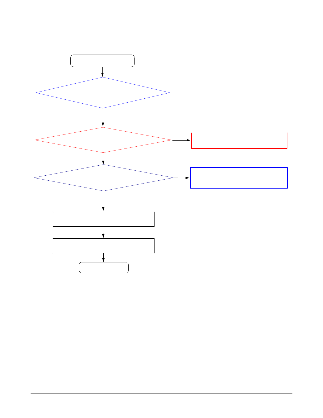
Initial
Initial Failure
Yes
Re-download SW the cell-phone.
Abnormal
Check the AP Reset
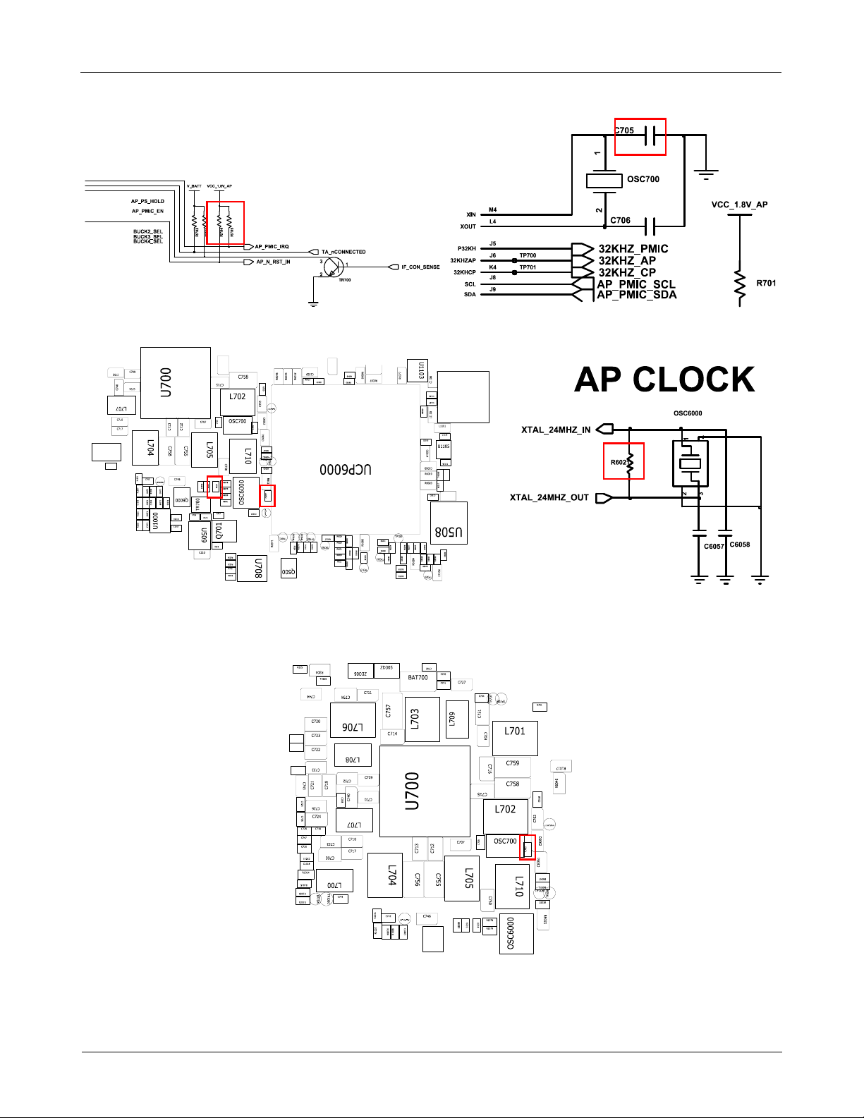
AP_N_RST_IN(R704)
Yes
Check the oscillator clock waveforms.
KHz:OSC700(C705),
32.768
Mhz:OSC6000(R6021)
24
=1.8
V(High)
No
Check the U700 and R704(crack, open, etc.)
No
Check the OSC700, OSC6000
Crack, open etc.)
(
Yes
Change UCP6000,U700
Abnormal
Change PBA
END
8-7
Confidential and proprietary-the contents in this service guide subject to change without prior notice.
Distribution, transmission, or infringement of any content or data from this document without Samsung’swritten authorization is strictly prohibited.
Level3Repair
8-8
Confidential and proprietary-the contents in this service guide subject to change without prior notice.
Distribution, transmission, or infringement of any content or data from this document without Samsung’swritten authorization is strictly prohibited.
Level3Repair
8-3-3.
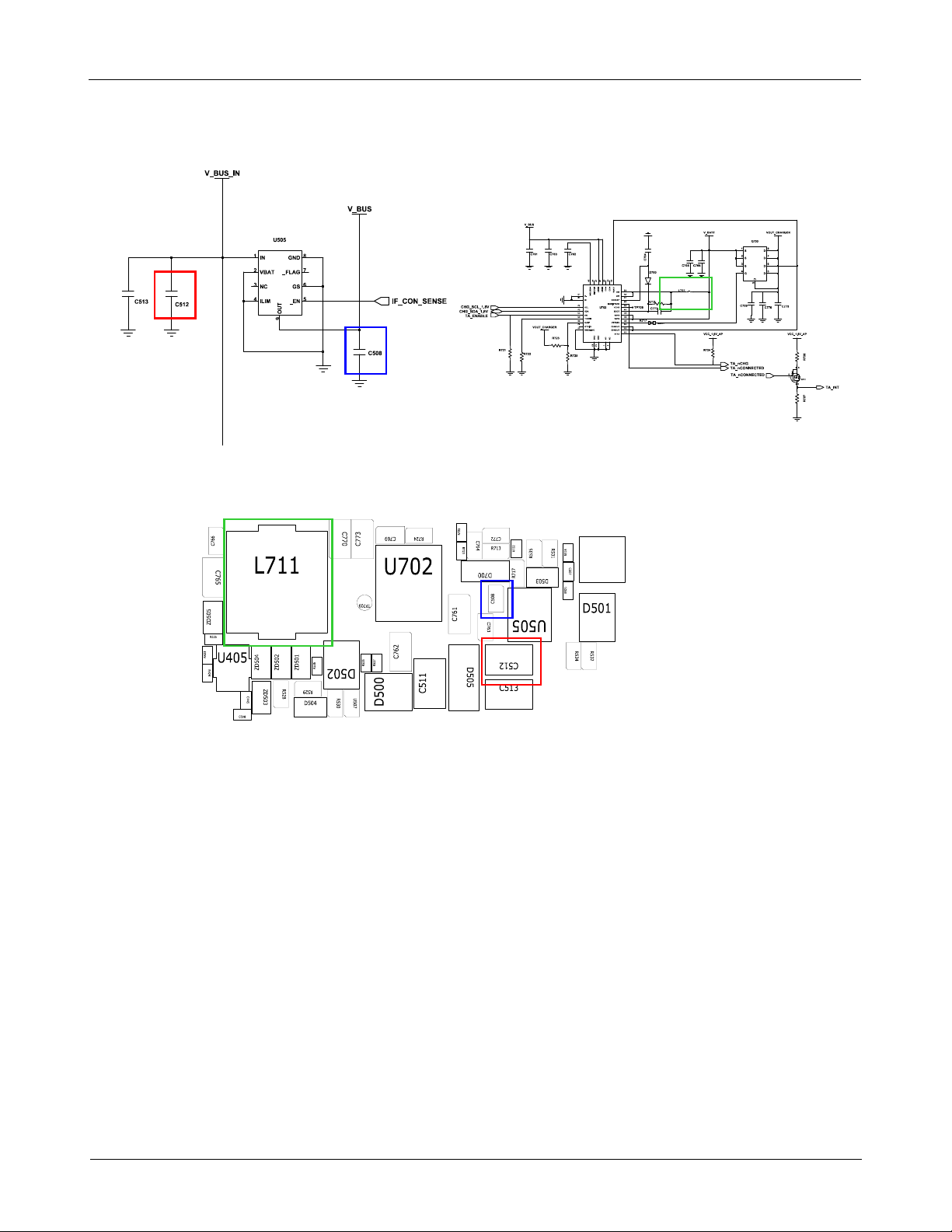
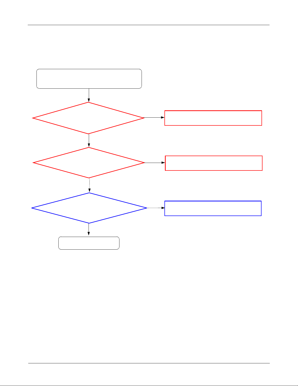
Charging Part
Check C512 whether voltage
Check C508 whether voltage
Waveform.(switching waveform)
Abnormal charging part
Yes
reading is greater than
Yes
reading is greater than
Yes
Check L711
4.7V
4.7V
No
No
No
Check the TA and the SLC500
TA or SLC500 may not be connected properly)
(
Check U505 chip
U505_OVP chip may not work)
(
Check L711(crack, open, etc.)
YES
Change U702
END
8-9
Confidential and proprietary-the contents in this service guide subject to change without prior notice.
Distribution, transmission, or infringement of any content or data from this document without Samsung’swritten authorization is strictly prohibited.
Level3Repair
8-10
Confidential and proprietary-the contents in this service guide subject to change without prior notice.
Distribution, transmission, or infringement of any content or data from this document without Samsung’swritten authorization is strictly prohibited.
Level3Repair
8-3-4.
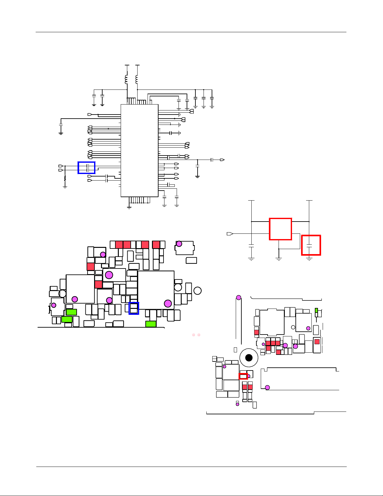
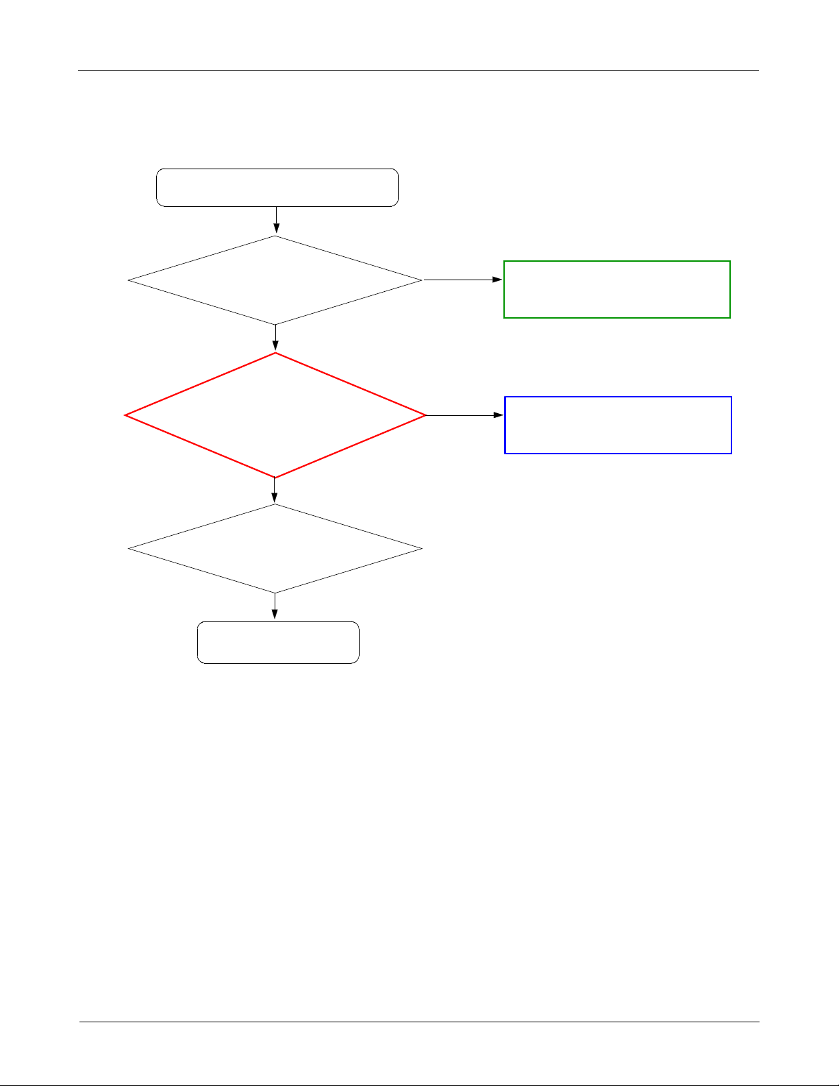
Microphone Part
Check main microphone function
in voice call speaker mode
or in Voice Recording mode
Check30pin FPCB module
where main MIC is placed
for any damage(Tear in FPC,
Check the voltage at
etc)
C403
Yes
Yes
=2.8V
No
No
Change the30pin FPCB module
Resolder or replace U400
Yes
Check component soldering
statuses of C435, C436
Yes
END
No
Resolder or replace C435, C436
8-11
Confidential and proprietary-the contents in this service guide subject to change without prior notice.
Distribution, transmission, or infringement of any content or data from this document without Samsung’swritten authorization is strictly prohibited.
Level3Repair
CODEC_LDO_EN
C430
SPEECH_PCM_CLK
SPEECH_PCM_SYNC
SPEECH_PCM_OUT
SPEECH_PCM_IN
MAIN_MIC_N
MAIN_MIC_P
2
1
4
R
MM_I2S_CLK
MM_I2S_SYNC
MM_I2S_DO
MM_I2S_DI
BT_PCM_CLK
BT_PCM_SYNC
BT_PCM_OUT
BT_PCM_IN
V_BATT
VCC_1.8V_AP
1
6
1
0
4
4
L
8
3
2
F
A
A
1
D
D
D
D
V
1
V
K
O
P
D
S
L
LDO1ENA
LDO2ENA
VREFC
DMICCLK
BCLK1
LRCLK1
DACDAT1
ADCDAT1
ADCLRCLK1|GPIO1
BCLK2
LRCLK2
DACDAT2
ADCDAT2
JACKDET
GPIO11|BCLK3
GPIO10|LRCLK3
GPIO8|DACDAT3
GPIO9|ADCDAT3
MICDET
IN1LP
IN1LN
IN2LP|VRXN
IN2LN|DMICDAT
IN1RP
IN1RN
IN2RP|VRXP
IN2RN
1
D
N
G
K
P
S
4
2
B
C
L
C425
C427
9
2
2
5
8
9
2
1
9
2
J
J
E
E
E
E
D
H
G
G
2
1
3
2
1
2
1
2
1
D
D
D
D
D
D
D
D
D
D
D
D
D
D
D
D
D
D
D
D
D
D
V
V
V
V
V
V
V
V
V
V
V
P
C
K
K
P
S
1
D
N
G
K
P
S
2
C
A
B
B
A
A
K
B
C
D
P
P
D
D
D
S
S
SCLK
ADDR
MCLK1
MCLK2
SPKMODE
REFGND
MICBIAS1
MICBIAS2
VMIDC
HPOUT2N
HPOUT2P
HPOUT1FB
HPOUT1R
HPOUT1L
U401
LINEOUT1N
LINEOUT1P
LINEOUT2N
LINEOUT2P
LINEOUTFB
SPKOUTLN
SPKOUTLN
SPKOUTLP
SPKOUTLP
SPKOUTRN
SPKOUTRN
SPKOUTRP
SPKOUTRP
CPCA
CPCB
CPVOUTN
2
2
D
D
D
CPVOUTP
D
N
N
N
D
N
D
G
G
G
N
N
G
2
K
K
C
C
G
P
P
P
G
P
S
N
N
D
C
A
S
H
3
8
9
5
9
2
1
D
K
K
H
D
C428
H3
SDA
H2
F3
TP_400
F1
F2
D5
A5
A9
A7
C431
E7
G8
H7
H6
J5
J6
C6
B6
C433
A6
B5
C434
C5
A1
B1
B3
B4
C1
D1
C3
D4
J8
K8
K7
J7
SPK_OUTL_N
SPK_OUTL_P
SPK_OUTR_N
SPK_OUTR_P
C438
C440
C439
C429
XTAL_24MHZ_AP
CODEC_CLK32K
EAROUT_FB
EAROUT_R
EAROUT_L
EAR_R_CRADLE
EAR_L_CRADLE
C426
CODEC_SDA_1.8V
CODEC_SCL_1.8V
C437
C446
LINEOUT_FB
V_BATT
MICBIAS_LDO_2.8V
C423
C424
A4
D6
F7
A8
TP_401
G3
G1
H1
F4
J1
K1
J3
G4
H4
K2
K4
G5
K3
J4
C435
C436
F9
D8
D7
C9
C8
C443
C7
B9
C444
B8
B7
U400
4
VDD
3
C402
U
CE
6
6
7
C
C
L711
7
6
5
5
0
5
D
Z
R526
2
4
0
0
5
5
U405
D
D
Z
Z
Z
R
D
5
2
5
8
0
C445
3
0
2
4
R
H
B
R
5
3
8
MICBIAS_EN
ZD405
D
4
0
4
Z
U
C
4
4
1
0
4
3
C409
8
0
4
D
Z
R403
8
R
4
0
9
C
4
4
2
2
R
0
5
2
0
5
C
0
R
5
2
2
2
L
E
T
S
_
R
A
U
_
T
P
8
R
0
5
U
5
0
R
5
6
0
R512
R
C
5
6
1
4
0
2
7
C6026
0
4
D
Z
4
0
U
U404
R
R
4
4
1
1
6
3
1
4
4
C
R411
C6030
0
0
0
6
E
2
0
4
R
9
3
4
C
C417
R
4
0
1
0
C
0
4
R400
0
0
R422
7
1
4
4
R
1
4
R
9
2
C
0
6
0
4
4
C
8
3
4
C
4
A
T
0
3
C
4
C
4
2
8
3
0
0
0
4
4
C431
L
L
C
4
3
4
4
1
0
0
4
4
C
C
4
4
C
4
5
3
4
C
R
4
R
1
2
4
1
5
6
3
C
4
8
2
0
6
C
M
U
D
4
0
6
8
C
1
4
0
C
2
4
ZD407
Z
5
4
0
0
4
4
L
L
9
8
1
1
4
4
R
R
U401
3
3
4
7
C
3
4
C
C446
F
9
0
C
4
1
9
C
4
2
1
4
3
4
C
1
0
9
2
L
C429
L
TP_400
4
0
6
1
0
4
_
P
T
C
4
C
C
2
5
4
4
2
2
6
7
C
4
2
C
4
1
4
1
2
4
3
L
S
C
1
0
2
1
2
4
R
8
3
0
6
R
R
0
0
5
R6024
R
7
5
0
R
3
5
0
1
0
5
0
2
C
C
5
0
0
0
C503
4
0
5
C
1
0
6
R
0
5
5
C402
U
5
0
0
4
C403
0
1
0
0
4
4
L50
D
D
Z
Z
C407
6
0
4
C
1
2
0
0
4
4
L
L
C405
C408
T
H
6
0
0
1
1
VOUT
2
GND
GND
5
C403
5
C
7
3
7
7
0
7
C
2
7
R
C
7
9
6
4
2
R
7
C
7
6
R
4
7
2
3
U702
9
T
0
7
P
1
0
5
7
2
2
5
6
5
5
3
R
R
5
D
0
2
5
D
R
Z
R
2
9
5
R
U
5
5
0
3
D504
7
0
0
1
6
7
C
2
6
7
C
D
5
0
1
5
1
0
5
0
C
5
D
5
0
S
L
C
8-12
Confidential and proprietary-the contents in this service guide subject to change without prior notice.
Distribution, transmission, or infringement of any content or data from this document without Samsung’swritten authorization is strictly prohibited.
Level3Repair
8-3-5.
Speaker Part
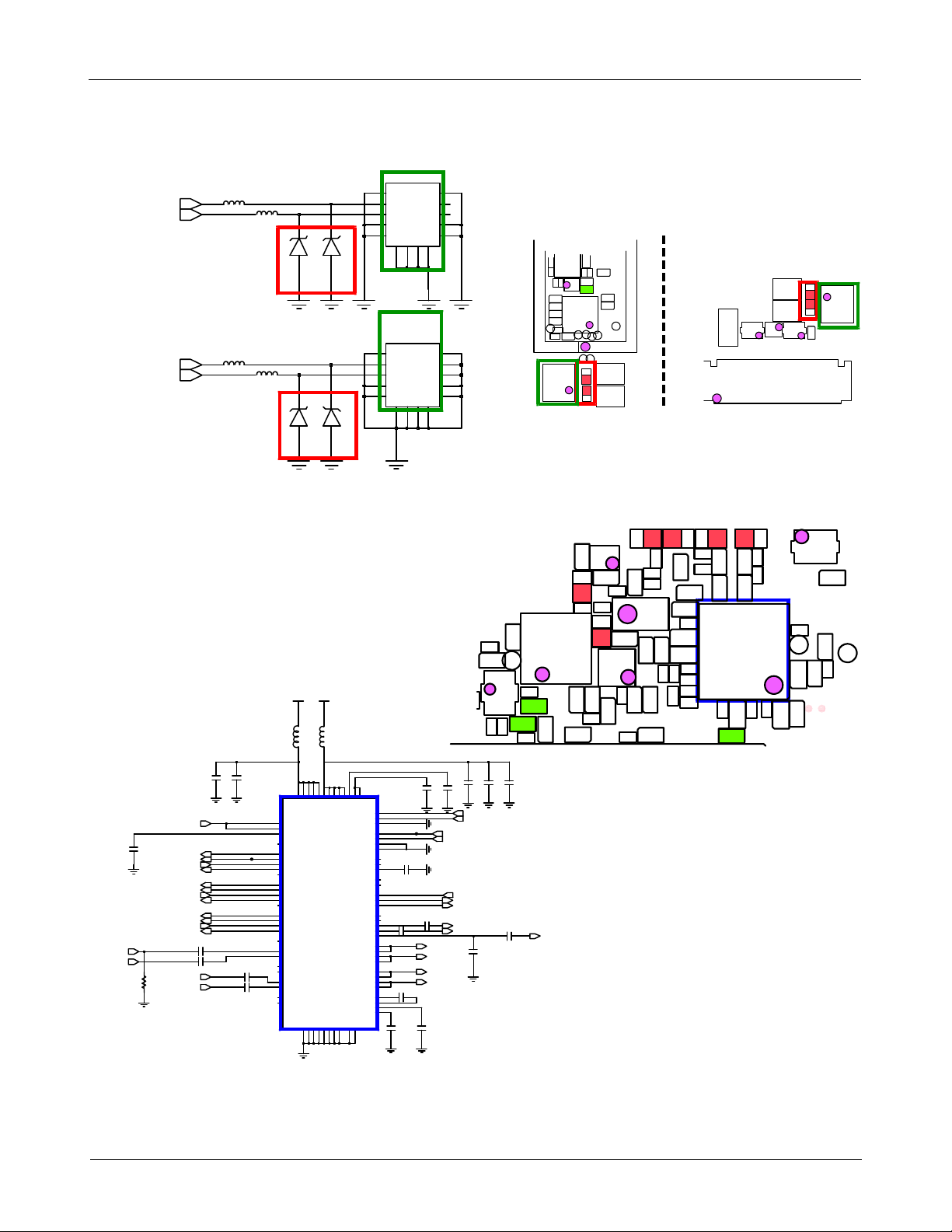
Play MP3 with maximum volume level.
ZD402, ZD403/D400, D401
Check speaker function.
Yes
Check the connection of
HDC400/HDC401
Yes
Check the signals on
Yes
No
Reconnect HDC400/HDC401
No
Resolder or replace U401
Replace the speaker
module
Yes
END
8-13
Confidential and proprietary-the contents in this service guide subject to change without prior notice.
Distribution, transmission, or infringement of any content or data from this document without Samsung’swritten authorization is strictly prohibited.
Level3Repair
SPK_OUTL_P
SPK_OUTL_N
SPK_OUTR_P
SPK_OUTR_N
L407
L409
L408
L410
HDC400
11
3344
55
7788
99
NC
0
0
4
D
11 12
11
3344
5566
788
7
99
NC
11 12
2
3
0
0
4
4
D
D
Z
Z
1
0
4
D
NCNC
13 14
HDC401
NCNC
13 14
NC
NC
22
66
1010
22
1010
3
1
1
2
0
2
U200
C
R
C
C
2
1
0
6
1
2
C
2
0
5
0
3
2
0
4
C200
2
0
2
P
T
R200
L200
6
2
0
0
2
9
C
C
C214
2
1
5
0
2
0
F
2
1
8
C
L
2
0
1
0
0
1
S
C
C
2
6
C201
C
U201
C
2
R
0
C202
H
D
C
4
0
1
P
6
2
T
0
4
0
P
2
T
0
7
2
P
T
TP201
P
3
2
T
0
TP200
5
0
P
2
T
L410
1
0
4
D
D
4
0
L409
0
C
8
1
F801
3
2
0
7
L
4
0
4
D
0
Z
0
4
Z
D
4
0
C
3
L
4
0
8
0
0
8
F
0
8
0
C
D
H
F802
5
1
8
C
S
L
MAIN_MIC_N
MAIN_MIC_P
C430
2
1
4
R
CODEC_LDO_EN
MM_I2S_CLK
MM_I2S_SYNC
MM_I2S_DO
MM_I2S_DI
SPEECH_PCM_CLK
SPEECH_PCM_SYNC
SPEECH_PCM_OUT
SPEECH_PCM_IN
BT_PCM_CLK
BT_PCM_SYNC
BT_PCM_OUT
BT_PCM_IN
ZD405
D
4
0
4
U
C
4
4
1
0
4
3
C409
8
0
4
D
Z
R403
8
R
4
0
9
C
4
4
2
2
R
0
5
2
0
5
C
0
C425
C426
CODEC_SDA_1.8V
CODEC_SCL_1.8V
EAROUT_FB
EAROUT_R
EAROUT_L
EAR_R_CRADLE
EAR_L_CRADLE
C437
0
R
5
2
2
C427
V_BATT
VCC_1.8V_AP
1
6
1
0
4
4
L
2
3
8
F
A
A
1
D
D
D
D
V
1
V
K
O
P
D
S
L
LDO1ENA
LDO2ENA
VREFC
DMICCLK
BCLK1
LRCLK1
DACDAT1
ADCDAT1
ADCLRCLK1|GPIO1
BCLK2
LRCLK2
DACDAT2
ADCDAT2
JACKDET
GPIO11|BCLK3
GPIO10|LRCLK3
GPIO8|DACDAT3
GPIO9|ADCDAT3
MICDET
IN1LP
IN1LN
IN2LP|VRXN
IN2LN|DMICDAT
IN1RP
IN1RN
IN2RP|VRXP
IN2RN
1
D
N
G
K
P
S
4
2
B
C
L
2
9
5
2
2
1
8
9
2
9
J
J
E
E
E
E
H
D
G
G
2
1
2
3
2
1
D
D
V
K
P
S
1
D
N
G
K
P
S
2
C
1
2
1
D
D
D
D
D
D
D
D
D
D
D
D
D
D
D
D
D
D
D
D
V
V
V
V
V
V
V
V
V
V
P
C
K
A
K
C
P
P
S
S
U401
2
2
D
D
D
N
N
N
D
G
G
N
G
K
K
P
G
P
P
C
A
S
S
9
3
9
K
D
D
H3
B
B
B
A
A
D
SDA
D
D
D
H2
SCLK
F3
ADDR
F1
MCLK1
F2
MCLK2
D5
SPKMODE
A5
REFGND
A9
MICBIAS1
A7
MICBIAS2
E7
VMIDC
G8
HPOUT2N
H7
HPOUT2P
H6
HPOUT1FB
J5
HPOUT1R
J6
HPOUT1L
C6
LINEOUT1N
B6
LINEOUT1P
A6
LINEOUT2N
B5
C434
LINEOUT2P
C5
LINEOUTFB
A1
SPKOUTLN
B1
SPKOUTLN
B3
SPKOUTLP
B4
SPKOUTLP
C1
SPKOUTRN
D1
SPKOUTRN
C3
SPKOUTRP
D4
SPKOUTRP
J8
C438
CPCA
K8
CPCB
K7
CPVOUTN
J7
D
CPVOUTP
N
D
G
N
2
C
P
C
G
N
H
N
D
8
5
2
1
H
K
C429
C428
TP_400
XTAL_24MHZ_AP
CODEC_CLK32K
C431
C433
SPK_OUTL_N
SPK_OUTL_P
SPK_OUTR_N
SPK_OUTR_P
C440
C439
C423
C424
A4
D6
F7
A8
TP_401
G3
G1
H1
F4
J1
K1
J3
G4
H4
K2
K4
G5
K3
J4
C435
C436
F9
D8
D7
C9
C8
C443
C7
B9
C444
B8
B7
2
L
U
P
S
A
T
_
E
R
_
T
8
R
0
5
5
U
R
5
6
0
R512
R
C
5
6
1
4
0
2
7
C6026
C446
LINEOUT_FB
0
4
D
Z
4
0
U
U404
R
R
4
4
1
1
6
3
1
4
4
C
R411
C6030
0
0
0
6
E
M
U
Z
2
0
4
R
9
3
4
C
C417
R
4
0
1
0
C
0
4
R400
0
0
R422
7
1
4
4
R
1
4
R
9
2
C
0
6
0
4
4
C
8
3
4
C
4
A
T
0
3
C
4
C
4
2
8
3
0
0
0
4
4
C431
L
L
C
4
3
4
1
4
0
0
4
4
C
C
4
4
C
4
5
3
4
C
R
4
R
1
2
4
1
5
6
3
C
4
8
2
0
6
C
D
4
0
6
8
C
1
4
0
C
2
4
ZD407
Z
5
4
0
0
4
4
L
L
9
8
1
1
4
4
R
R
U401
3
3
4
7
C
3
4
C
C446
0
F
1
C
4
1
9
C
4
2
1
C
4
4
2
3
4
4
C
9
2
0
9
L
C429
L
TP_400
4
0
6
1
0
4
_
P
T
C
4
C
C
2
5
4
4
2
2
6
7
C
1
4
1
2
4
3
L
8-14
Confidential and proprietary-the contents in this service guide subject to change without prior notice.
Distribution, transmission, or infringement of any content or data from this document without Samsung’swritten authorization is strictly prohibited.
Level3Repair
8-3-6.
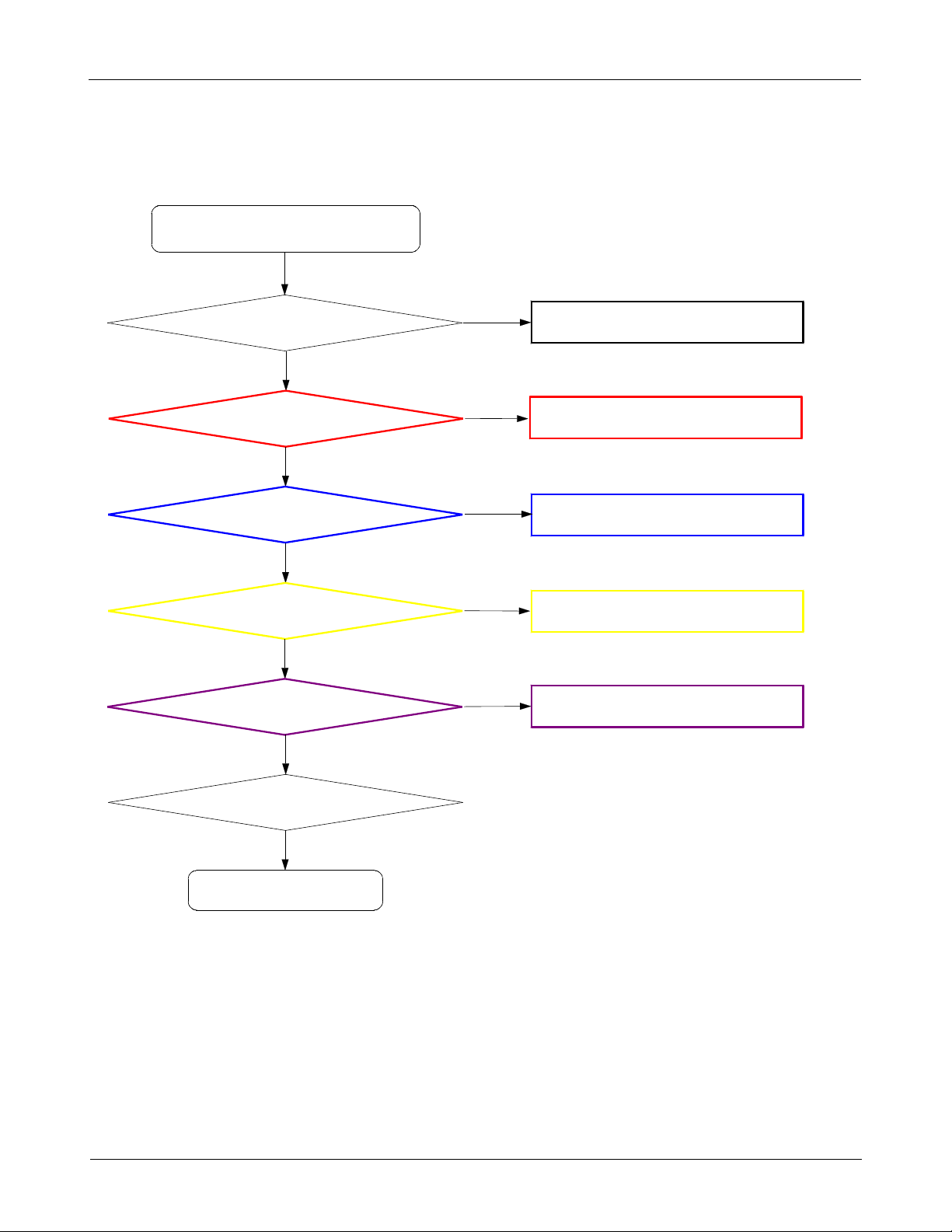
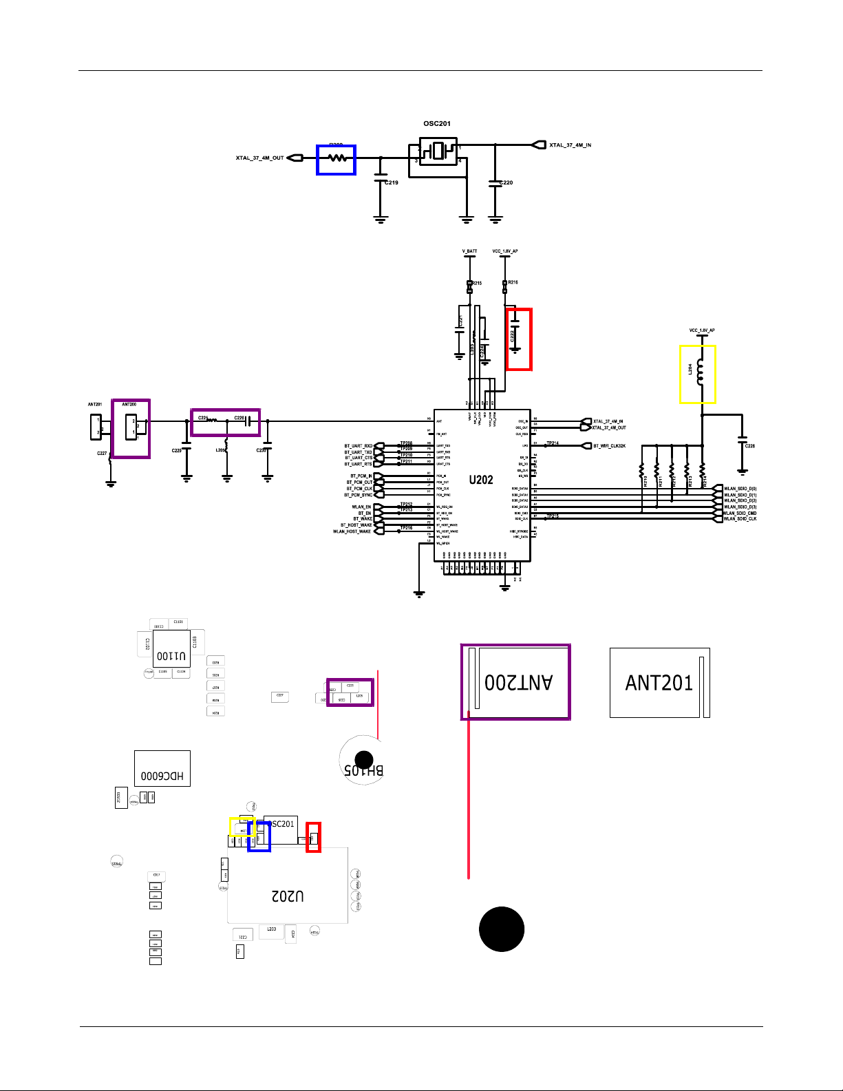
BT/WIFI
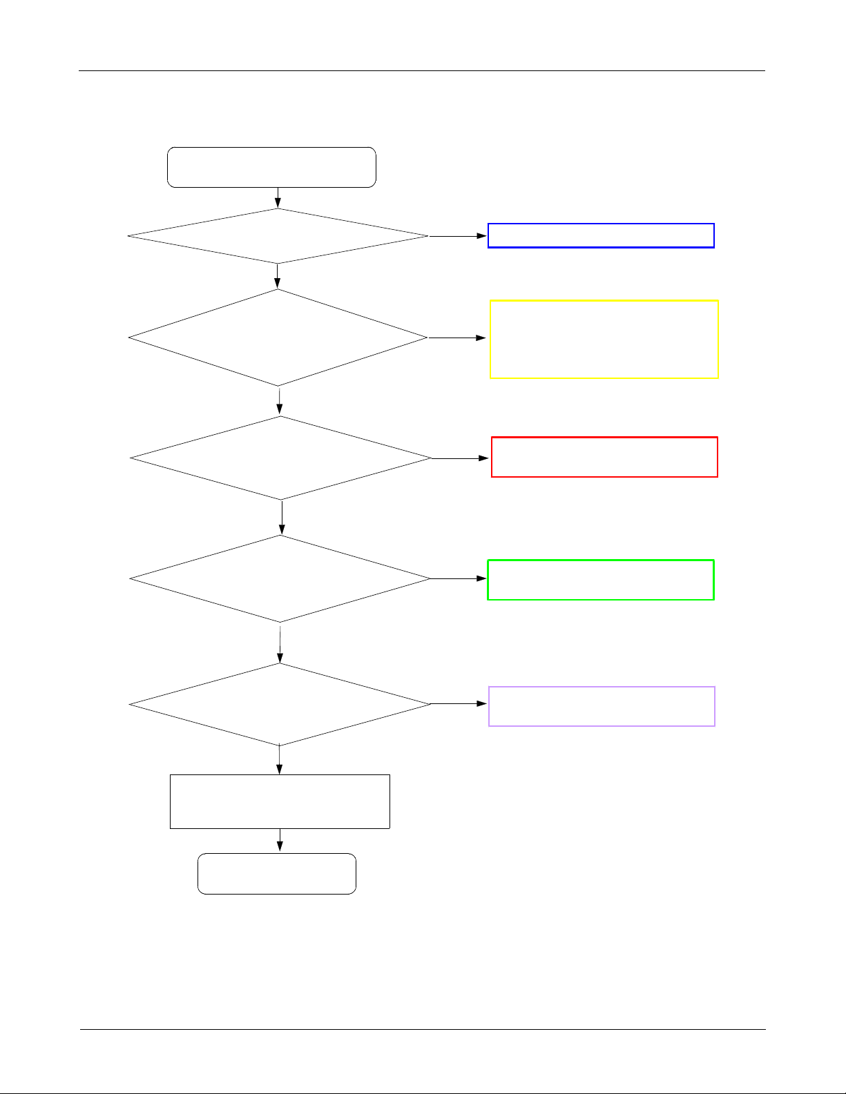
BT/WiFi is not working
Yes
Check BT or WiFi function
Check the Voltage on C222
Check
ON
Yes
1.8V
Yes
MHz Clock at
37.4
R209
Yes
No
=
No
No
Enable BT or WiFi Function
Check AP PMIC(U700)
Check OSC201
heck the Voltage on L204
C
C225,C226, ANT200
Resolder or Replace U202
1.8V
Yes
Check the Status of
Yes
Yes
END
=
No
No
Resolder or change L204
Resolder or Replace C225,C226, ANT200
8-15
Confidential and proprietary-the contents in this service guide subject to change without prior notice.
Distribution, transmission, or infringement of any content or data from this document without Samsung’swritten authorization is strictly prohibited.
Level3Repair
8-16
Confidential and proprietary-the contents in this service guide subject to change without prior notice.
Distribution, transmission, or infringement of any content or data from this document without Samsung’swritten authorization is strictly prohibited.
Level3Repair
8-3-7.
S-Pen
S-Pen"function does not work
"
Yes
Check the S-Pen
connector on Main PBA
Abnorma
Check the voltage
C907
=3.3V
Yes
Check C935, C942 is
MHz
20
Yes
No
No
No
Reconnect the CN900
Resolder R913, U902, C907, L900, L901
Replace the PBA
Resolder C935, C942, OSC900
Replace the PBA.
Check I2C mode
R909=HIGH, R930=open
R907, R908=HIGH
Yes
Check the PDCT, IRQ line
PDCT R926=High
IRQ R923=LOW
Yes
Replace the LCD ass'y
Yes
END
No
No
Resolder R909, R930, R907, R908, U901
Replace the PBA
Resolder R926, R923, U900
Replace the PBA.
8-17
Confidential and proprietary-the contents in this service guide subject to change without prior notice.
Distribution, transmission, or infringement of any content or data from this document without Samsung’swritten authorization is strictly prohibited.
 Loading...