

Page 1

Level
8.
Block Diagram
8-1.
Repair
3
VSMPS2_1V8
MAIN LCD
4.27", AMOLED
(qHD OCTA)
OCTA TSP MODULE
PHONE REMOTE CONTROL
VPS_L
VPS_R
VPS SW
DG2750DN-T1-E4
EARSPK_L
EARSPK_R
EARPHONE
EAR_3.5_DET EAR_ADC
VPS SW
DG2750DN-T1-E4
EAR_DET
This goes to GPIO of AP
(MSM8230)
LCD
VREG_L25_1P2_MSM
VREG_S4_1P8
EARSPK_L_CODEC
EARSPK_R_CODEC
EAR_MIC_M
EAR_MIC_P
PHONE MEMORY
LCD BACK LIGHT
AMOLED LCD / OCTA TSP
CAMERA
8Mega AF
CAMERA
VGA
ICE40LP1K-CM36
This goes to USB SW
TSP_AVDD_3.3V
TSP_DVDD_1.8V
VCI_2.8V
IOVDD_1.8V
CAM
FLASH
FPGA
HALL IC
S-5712ACDL1-
I4T1U
VMEM_3V3
VT_CAM_MCLK
MIPI_CSI0_CLK_P_F
MIPI_CSI0_CLK_M_F
I2C3_CLK_CAM
VT_CAM_MCLK
MIPI_CSI1_CLK_P_F
MIPI_CSI1_CLK_M_F
I2C3_CLK_CAM
VDD_MOT_3V0
DETECT_FLIPCOVER
TOUCH_KEY_2.2V
Audio
Codec
SPK_OUT_P / SPK_OUT_N
RP114K331D-TR
RICOH
SDC1_CLK
MC2_DAT_[0:7]
STOD30TPQR
MIC2871YMK
RP507K
TOUCH_IO_1.8V
KEY_LED_3.3V
RX_I2S_DO / TX_I2S_DI
MAIN MIC M/P
RCV_P / RCV_N
MIPI_DSI0_CLK_P_F
MIPI_DSI0_CLK_M_F
M
LINEAR MOTOR
AUDIO_MCLK
CODEC_RST
CODEC_INT
I2C_CLK_CODEC
I2C_DATA_CODEC
RX_I2S_SCK
RX_I2S_WS
TX_I2S_SCK
TX_I2S_WS
SUB MIC M/P
MC2
MIPI
DSI0
H
H
C
C
U
U
O
O
T
T
_
_
A
K
T
L
A
C
D
_
_
C
C
2
I
2
I
TOUCH KEY
19MHz
XO_THERM
MIC
Main Power Supply
MIC
RECIEVER
SPK
Y
E
K
_
E
M
O
H
GPIO
SD- CARD
SIM 1
SIM 2
MSM8230
AP + CP
Qualcomm
I2C
System control IF
PM8917
(BB / PMU)
P
h
o
n
e
R
e
s
e
t
PORN
Phone Reset
RF BB IF
SDIO
UART
I2C
I2C
DP DM
TSU6721
U-USB SW IC
Power on KEY
MUS_SCL
MUS_SDA
Updated Date : 2013.01.04
RF BLOCK
RX_DA,TX_DA
SYS_CLK_REQ /
RF_STOBE / SCLK / SDAT
BT_DATA,CTL,SSBI
FM_DATA,SSBI
WL_CMD_DATA,CLK,SET
WLAN_BB_IQ
WCN_XO
NFC_CLK,DATA
NFC_VEN
I2C_CLK_SENS
I2C_CLK_COMPASS
USB_DM
ICMEF112P120
USB_DP
PTVS18V
FT7521L6X
RESET IC
Fairchild
FPGA_MAIN_CLK
Transceiver
WTR2605
BT/WIFI/FM
WCN3660
WIFI
Qualcom m
ICE40LP1K-CM36
FPGA
LATTIC
PRX_MB3
RF_TX_DA_2, 3
PN547
NFC
STE
YAS532B-PZE2
E-COMPASS
YAMAHA
VBUS
USB_ID
V_BAT_FET
Micro USB CON
RF_TX_DA_1
Duplexer x4
OSC
48MHz
27.12MHz
2in1 SAW
TCXO
AF88A
AWT6751
AWT6755
PDET_IN
DPX165950DT
3G PA
Diplexer
WCDMA_B1/2/5/8RX_B1/2/5/8
NFC_CLK_I/O
MPU-6500
Invensense
ACCEL
2013 1 11
Tx Module
Coupler
SKY77573
LDJ18829M24AD011
ANT_CPL_OUT
GPS/GNSS
SFHG89DQ
GPS ANT
102
GPS_IN
BT / WIFI /FM
FM_I2S_DO
FM_I2S_CLK
FM_I2S_SYNC
FM_I2S_DI
LNA/Filter
ANT
8-1
Confidential and proprietary-the contents in this service guide subject to change without prior notice.
Distribution, transmission, or infringement of any content or data from this document without Samsung’swritten authorization is strictly prohibited.
1
Page 2
Level3Repair
PCB Diagrams
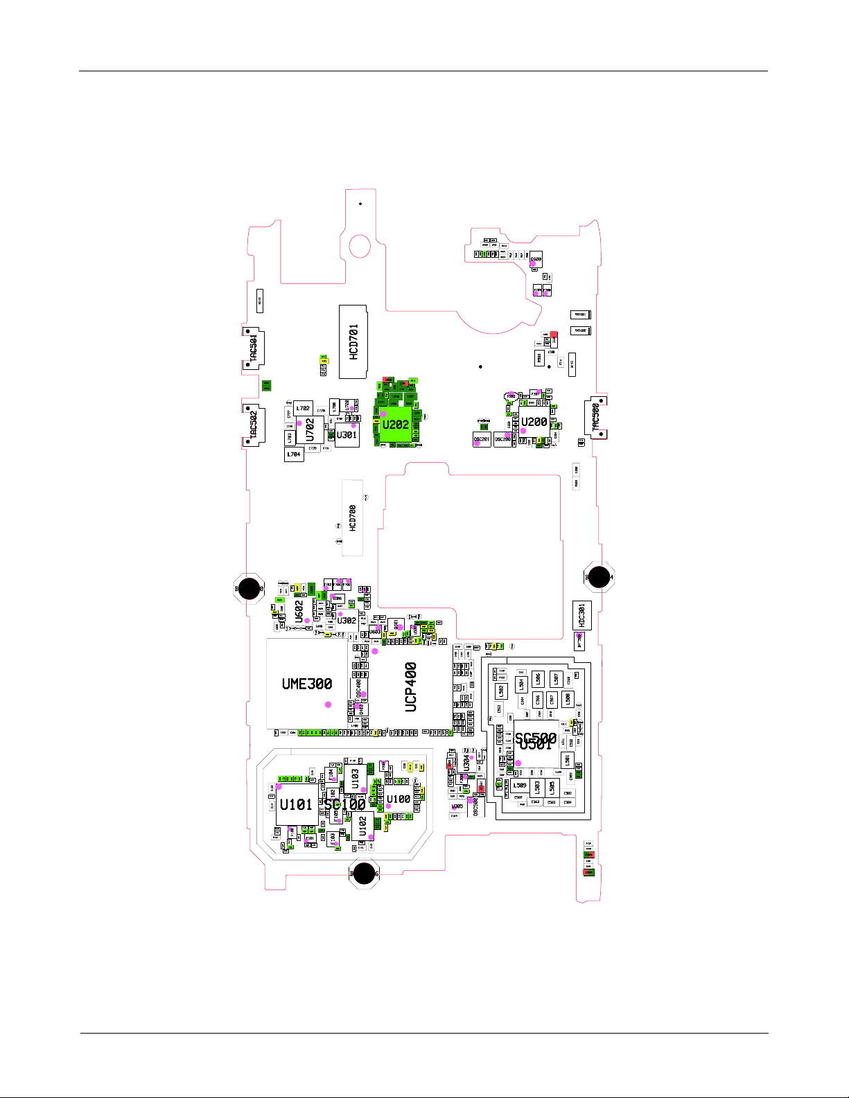
8-2.
8-2-1.
Top
8-2
Confidential and proprietary-the contents in this service guide subject to change without prior notice.
Distribution, transmission, or infringement of any content or data from this document without Samsung’swritten authorization is strictly prohibited.
Page 3
Level3Repair
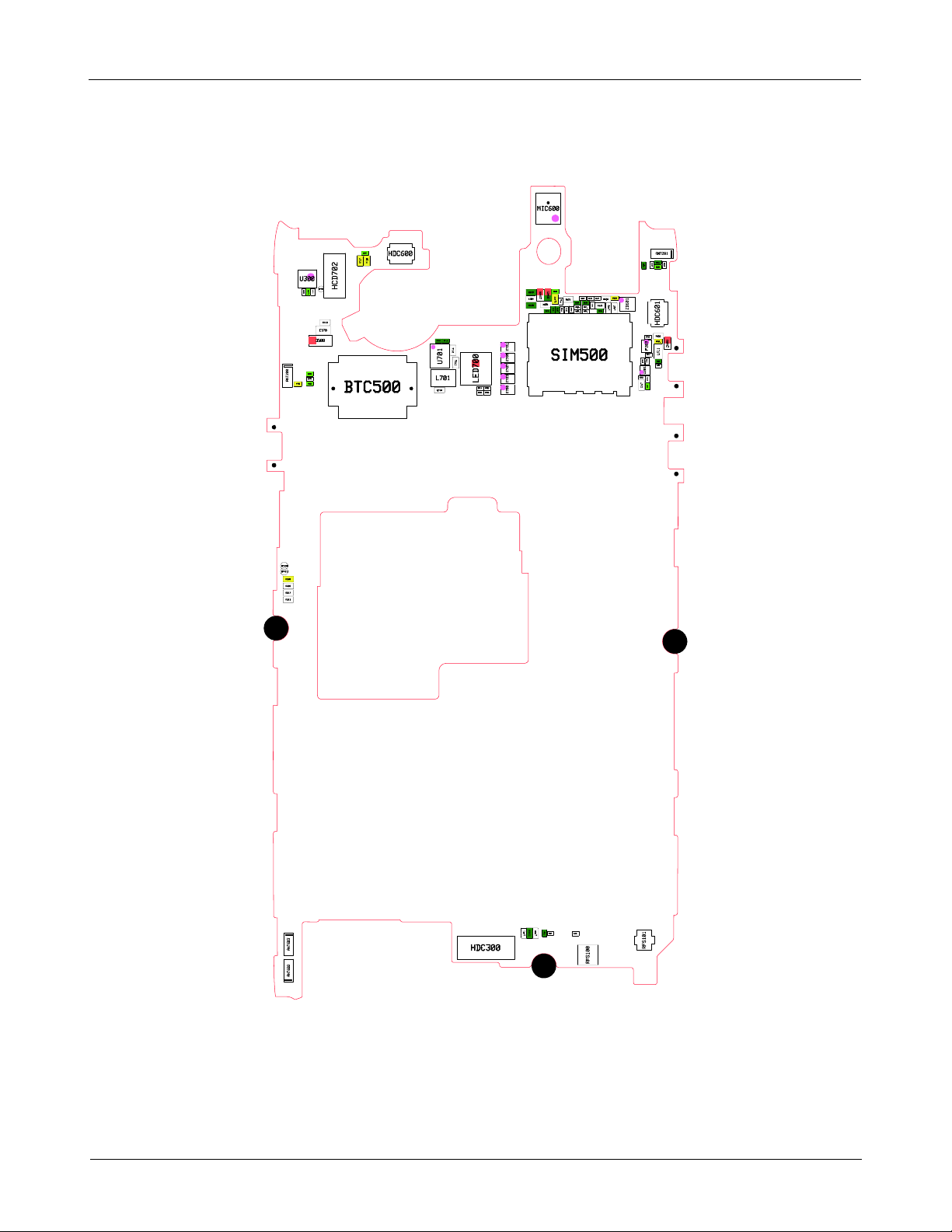
8-2-2.
Bottom
8-3
Confidential and proprietary-the contents in this service guide subject to change without prior notice.
Distribution, transmission, or infringement of any content or data from this document without Samsung’swritten authorization is strictly prohibited.
Page 4

Level3Repair
Flow Chart of Troubleshooting
8-3.
Equipments
Oscilloscope
Power Supply
Digital Multi-meter
driver, ESD Safe Tweezer
+
8960 &
Confidential and proprietary-the contents in this service guide subject to change without prior notice.
Distribution, transmission, or infringement of any content or data from this document without Samsung’swritten authorization is strictly prohibited.
Spectrum Analyzer
8-4
Soldering iron
Page 5
Level3Repair
8-3-1.
Power On
Mobile phone does not power on.
Check the Battery Voltage
it more than
Is
Yes
Power-on the phone and
check the power-on sound
or motor Vibration.
No
Check the TAC500
soldering crack, open, etc)
(
3.8
V?
.
No
Yes
Abnormal
If its voltage level is extremely low(under
Change the TAC500(Power-key switch)
Charging the battery by TA.
Change the battery.
Change the FRONT-LCD ASSY
And retry to the power-on operation.
3.0
V),
Yes
Check the U500 output voltage
R503
(
Check the Clock OSC500
Is that frequency19Mhz?
check the initial operation
>1.15
V,R504
Yes
Yes
Yes
END
>1.05
V)
No
No
If the output voltage is not satisfied with normal
condition, Change the U500.
Each voltage level has
Change the OSC500.
Test condition(Oscilloscope setting)
us.div(time division)
:20.0
±10%
margin.
8-5
Confidential and proprietary-the contents in this service guide subject to change without prior notice.
Distribution, transmission, or infringement of any content or data from this document without Samsung’swritten authorization is strictly prohibited.
Page 6

Level3Repair
T
C
PHONE_ON_N
PM_RESIN_N
TAC500
1
2
C576
VR500
S1S2
POWER KEY
3
NC
4
NC
5
NC
6
NC
19M_OUT
19M_IN
VREG_S4_1P8
R501
R505
R502
6
5
4
U500
NC
OUTVDD
VSS
OSC500
2
VREG_S4_1P8
3
0
5
R
1
2
3
IN+IN-
R504
1
43
19MHz
BATT_IN
BATT_ID
VREF_XO_THM
R508
XO_THERM
C520
GND_XOAD
8-6
Confidential and proprietary-the contents in this service guide subject to change without prior notice.
Distribution, transmission, or infringement of any content or data from this document without Samsung’swritten authorization is strictly prohibited.
Page 7

Level3Repair
8-7
Confidential and proprietary-the contents in this service guide subject to change without prior notice.
Distribution, transmission, or infringement of any content or data from this document without Samsung’swritten authorization is strictly prohibited.
Page 8
Level3Repair
8-3-2.
Initial
Initial Failure
Yes
Re-download latest SW on the
mobile phone.
Abnormal
Re Check
Trouble shooting process
Change UME300
Change PBA
"8-3-1
Power on"
Normal
Abnormal
Abnormal
Check the OSC500(Crack, open etc.)
Check the U500(Crack etc)
END
8-8
Confidential and proprietary-the contents in this service guide subject to change without prior notice.
Distribution, transmission, or infringement of any content or data from this document without Samsung’swritten authorization is strictly prohibited.
Page 9
Level3Repair
8-9
Confidential and proprietary-the contents in this service guide subject to change without prior notice.
Distribution, transmission, or infringement of any content or data from this document without Samsung’swritten authorization is strictly prohibited.
Page 10

Level3Repair
8-3-3.
No Service
No service
Yes
Check memu setting
Menuapplicationssettingwireless and network
mobile networksnetwork modesetting is auto mode
MenuPhoneKeypad
*#1234#
Check the L100,L101,L104,L105
check Phone version
PHONE:I9192XXXX
No
is well soldered
?
PHONE:I9192XXXX
Check the Main Antenna exists or not
No
Re-solder L100,L101 ,L104,L105 correspondingly.
Yes
Check VREF
VREF(C109)
Change the Main Antenna
Change the PBA
=2.0V
Abnormal
Abnormal
Yes
END
No
Replace the U501
8-10
Confidential and proprietary-the contents in this service guide subject to change without prior notice.
Distribution, transmission, or infringement of any content or data from this document without Samsung’swritten authorization is strictly prohibited.
Page 11
Level3Repair
r
VWTR_RF1_1.3V
VWTR_RF2_2.0V
3
1
1
R100
R
C100
VWTR_IO_1.8V
C101
RX_B8_G900
RX_B5_G850
RX_DCS_PCS
PRX_BB_IP
PRX_BB_IM
PRX_BB_QP
PRX_BB_QM
GPS_IN
GNSS_BB_IP
GNSS_BB_IM
GNSS_BB_QP
GNSS_BB_QM
GP_DATA0
GP_DATA1
RX_B1
RX_B2
3
4
2
0
0
0
1
1
1
C
C
C
5
RX_LB1_IN
10
RX_LB2_IN
4
RX_MB1_IN
9
RX_MB2_IN
3
RX_MB3_IN
61
RX_BB_IP
55
RX_BB_IM
49
RX_BB_QP
43
RX_BB_QM
11
GNSS_RF_IN
62
GNSS_BB_IP
51
GNSS_BB_IM
45
GNSS_BB_QP
41
GNSS_BB_QM
53
GP_DATA0
58
GP_DATA1
57
GP_DATA2
C
N
D
6
3
0
0
7
6
5
1
0
0
0
L
1
1
1
C
C
C
7
1
1
C
8
1
1
0
2
6
0
0
9
6
9
6
4
3
2
4
5
4
3
2
1
2
3
1
L
L
L
G
I
D
_
1
F
R
_
D
D
V
A
A
B
O
O
O
O
L
L
L
L
L
L
B
D
N
C
P
P
P
_
_
_
_
_
L
V
_
_
_
T
_
T
R
G
R
_
T
_
1
R
_
G
_
_
_
R
_
1
_
2
F
_
1
1
2
_
1
2
F
1
F
F
F
F
R
1
F
F
F
R
_
R
R
R
R
F
R
_
R
_
R
_
_
_
D
R
_
_
_
D
D
D
D
D
_
D
D
D
D
D
D
D
D
D
V
D
D
D
D
V
V
V
V
V
D
V
V
V
V
U100
D
D
D
D
D
D
D
D
D
D
D
N
N
N
N
N
N
N
N
N
N
N
G
G
G
G
G
G
G
G
G
G
G
7
8
5
4
9
5
7
2
4
3
5
8
2
2
2
1
2
1
1
3
3
3
3
3
Tranceive
C112
1
0
9
8
0
1
1
0
0
1
1
L
1
1
1
1
C
C
C
C
8
1
1
C
9
4
7
5
5
3
L
O
O
O
I
L
X
C
_
P
_
3
V
_
2
_
F
T
F
T
R
_
R
_
_
2
_
2
D
F
F
D
D
R
R
D
_
V
_
7
V
D
D
TX1_OUT
D
D
V
V
TX2_OUT
TX3_OUT
TX_BB_IP
TX_BB_IM
TX_BB_QP
TX_BB_QM
PDET_RFFB_IN
SSBI_RX
SSBI_TX_GNSS
RF_ON
XO_IN
DAC_REF
NC
NC
D
D
D
D
D
N
N
N
N
N
G
G
G
G
G
0
2
4
7
5
4
4
4
1
6
2
12
18
23
22
8
56
13
60
24
63
64
TP_SSBI_2
TP_SSBI_1
C127
RF_TX_DA_1
RF_TX_DA_2
RF_TX_DA_3
TX_BB_IP
TX_BB_IM
TX_BB_QP
TX_BB_QM
PDET_IN
SSBI_RX
SSBI_TX_GNSS
RF_ON
DAC_REF
C128
Near WTR2605
R102
RX_DCS_PCS
WTR_XO_A0
L104
L106
L105
C126
F101
1
6
IN1
OUT
9
IN2
G
G
G2G3G45G
G
78
10
L109
Near WTR2605
8-11
Confidential and proprietary-the contents in this service guide subject to change without prior notice.
Distribution, transmission, or infringement of any content or data from this document without Samsung’swritten authorization is strictly prohibited.
Page 12
Level3Repair
8-3-4.
Sim Part
Insert SIM card
Yes
Is SIM/SD assy well
connected to main board?
Yes
Check the SIM Voltage.
C574)
(
>= 1.8or3.0?
Yes
Check the SIM Voltage.
R702)
(
>= 1.8or3.0?
Yes
No
No
No
Reassemble SIM/SD assy and still SIM
does not work, replace SIM/SD assy
Change to the new SIM card.
If it doesn`t still work SIM card after changing
the SIM card, Check the SIM500(Crack etc)
Change to the new SIM card.
If it doesn`t still work SIM card after changing
the SIM card, Replace the PBA
END
8-12
Confidential and proprietary-the contents in this service guide subject to change without prior notice.
Distribution, transmission, or infringement of any content or data from this document without Samsung’swritten authorization is strictly prohibited.
Page 13

Level3Repair
8-13
Confidential and proprietary-the contents in this service guide subject to change without prior notice.
Distribution, transmission, or infringement of any content or data from this document without Samsung’swritten authorization is strictly prohibited.
Page 14
Level3Repair
8-3-5.
Charging Part
TA/USB Insert
Charging Sequence Start
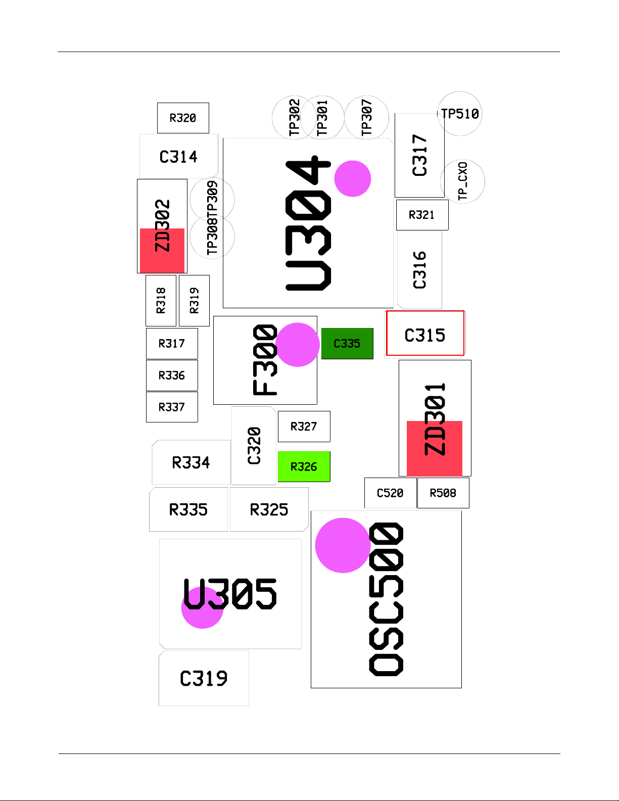
C315
C315
Yes
=5V
Yes
=5V?
Yes
END
No
No
Reconnect TA or USB
Change U712
USB_HS_D_P
USB_HS_D_M
VPS_L
VPS_R
UART_RXD
5
A
S
U
B
V
VUSB_FET_5V
4
2
A
A
T
O
I
U
D
O
D
V
C
C
N
N
1
2
VREG_S4_1P8
VREG_S4_1P8
C317
C316
C2
SCL
B2
SDA
D5
ID
C5
DP
B5
DM
A1
INTB
A3
ISET
E4
JIG
E3
BOOT
R321
TP307
VBATT_CON
VUSB_FET_5V_CON
C314
TP301
TP302
TP303
TP304
R320
TP308
TP309
C315
1
D
T
A
B
V
B1
DP_HT
C1
DM_HT
D2
IDBP
B3
S_L
C4
S_R
B4
MIC
D4
GND
C3
VBUS_CAP
D3
GND
E2
TXD
E1
RXD
D
N
G
5
E
Micro-USB Switch
MUS_SCL
MUS_SDA
USB_ID
MUSB_INT
CHG_DET
JTAG_JIG_ON_N
JIG_ON_N
UART_BOOT_ONUART_TXD
I2C4_DATA_TOUCH
I2C4_CLK_TOUCH
V_BUS_JTAG_ID
F300
1
I|O
23
I|O
4
I|O
I|O
D
D
N
N
G
G
6
5
USB_DP
USB_DM
MAIN_THM_1
USB_DP
USB_DM
USB_ID
8-14
Confidential and proprietary-the contents in this service guide subject to change without prior notice.
Distribution, transmission, or infringement of any content or data from this document without Samsung’swritten authorization is strictly prohibited.
Page 15
Level3Repair
8-15
Confidential and proprietary-the contents in this service guide subject to change without prior notice.
Distribution, transmission, or infringement of any content or data from this document without Samsung’swritten authorization is strictly prohibited.
Page 16

Level3Repair
8-3-6.
Microphone Part
Check microphone function
in voice call receiver mode
or in Voice Recording mode
Check the main MIC is
placed for any damage
Check the voltage at
L304
Yes
Yes
=1.8V
No
No
Resolder the main MIC
Resolder or replace L304
If the voltage level is not fixed, then
you have to change MIC on SUB PCB
END
Yes
8-16
Confidential and proprietary-the contents in this service guide subject to change without prior notice.
Distribution, transmission, or infringement of any content or data from this document without Samsung’swritten authorization is strictly prohibited.
Page 17

Level3Repair
I2C4_DATA_TOUCH
I2C4_CLK_TOUCH
MAIN_THM_1
USB_DP
USB_DM
V_BUS_JTAG_ID
USB_ID
TOUCH_IO_1.8V
R318
R336
R337
ZD302
R319
VREG_FEM/GPS_2P85
1
0
3
L
TOUCH_KEY_2.2V
KEY_LED_3.3V
C331
VUSB_FET_5V_CON
C335
ZD301
HDC300
11
33
55
7788
99
11111212
13 13 14
15151616
17 17 18
1919
21 21 22
23232424
2525
27 272828
29
29
C
C
N
N
2
1
3
3
MIC_BIAS1_1.8V
L304
TOUCH_IO_1.8V
2
2
4
4
6
6
10
10
14
18
20
20
22
26
26
30
30
C
C
N
N
4
3
3
3
R317
L300
0
0
C324
3
D
Z
TK&IF&MAIN MIC. Connector
MAIN_MIC_P
MAIN_MIC_M
TOUCHKEY_INT
HOME_KEY
SWITCHABLE_ANT1
C320
R327
VBATT_CON
R334
R335
U305
B1
A1VOUT
VOUT
B2
A2
VIN
VIN
C2
C1
GND
ON
C
C
N
N
1
R325
R326
2
9
1
3
C
8-17
Confidential and proprietary-the contents in this service guide subject to change without prior notice.
Distribution, transmission, or infringement of any content or data from this document without Samsung’swritten authorization is strictly prohibited.
Page 18

Level3Repair
8-3-7.
Speaker Part
Play MP3 with maximum volume level.
Check speaker function.
Yes
Check the connection of
Speaker module
Yes
Check the signals on
L607, L612
No
No
Reconnect speaker or replace speaker
module
Replace SPK
Yes
Check the signals on
C640, C641
Yes
END
No
Replace U 602
8-18
Confidential and proprietary-the contents in this service guide subject to change without prior notice.
Distribution, transmission, or infringement of any content or data from this document without Samsung’swritten authorization is strictly prohibited.
Page 19

Level3Repair
SPK_OUT_P
SPK_OUT_N
L607
L612
0
4
6
C
SPK
ANT602
1
1
2
2
1
ANT603
1
3
0
1
6
4
D
6
Z
C
2
4
0
6
D
Z
2
8-19
Confidential and proprietary-the contents in this service guide subject to change without prior notice.
Distribution, transmission, or infringement of any content or data from this document without Samsung’swritten authorization is strictly prohibited.
Page 20

Level3Repair
8-3-8
Receiver Part
Check receiver function
in voice call receiver mode.
Yes
Check the receiver module
for any damage(tear in
FPCB, crack, etc)
No
Check the signals on C620,
C621
Yes
END
Yes
Replace receiv er module
No
Replace U 602
8-20
Confidential and proprietary-the contents in this service guide subject to change without prior notice.
Distribution, transmission, or infringement of any content or data from this document without Samsung’swritten authorization is strictly prohibited.
Page 21

Level3Repair
PS_ALS_SCL
PS_ALS_SDA
PS_INT
VREG_LVS4_1P8
R620
R621
VREG_L9_2P85
3
2
2
2
6
6
C
C
VREG_LVS4_1P8
VREG_L16_3P0
R622
HDC600
11
33
55 6 6
77 8 8
99
NC
NC
12 13
11
4
2
6
C
NCNC
10 10
14
VDD_IR_LED_3.3V
22
44
R617
R618
R619
R623
R624
R625
R626
1
0
0
0
6
R
V
1
0
2
2
6
R
6
6
V
C
C
Q600
1G
3
S
D
2
IRDA_CTRL
RCV_P
RCV_N
R628
8-21
Confidential and proprietary-the contents in this service guide subject to change without prior notice.
Distribution, transmission, or infringement of any content or data from this document without Samsung’swritten authorization is strictly prohibited.
Page 22

Level3Repair
8-3-9.
BT/WIFI
BT/WiFi is not working
Yes
Check BT or WiFi function
ON
Yes
Check the Status of
C229,C228,ANT200
Yes
Replace BT/WIFI Antenna
Yes
No
No
Enable BT or WiFi Function
Resolder or Replace
C229,C228,ANT200
VDD_WLAN_1P3
END
VREG_L10_3P0
0
2
2
C
CLK_OUT
XO_IN
XO_OUT
BT_SSBI
BT_DATA
BT_STROBE
FM_DATA
FM_SSBI
FM_HS_RX
FM_TXRX
WL_BB_IN
WL_BB_IP
WL_BB_QP
WL_BB_QN
VDD_5GWLAN_3P3
VREG_S2_1P3
VDD_WLAN_1P3
VDD_5GWLAN_3P3
C216
C217
WL_CMD_SET
WL_RFIO_5G
WL_CMD_DATA0
WL_CMD_DATA1
WL_CMD_DATA2
WL_CMD_CLK
VLDO_1P8
C224
VREG_LVS1_1P8
C218
WL_RFIO_5G
C219
F200
IN
GND1 GND2
1
C264
2
OUT
L202
3
4
W
O
L
1
G
2
3
ANT
G
5
F201
G
H
G
I
H
6
C228
L203
ANT200
1
C229
1
2
2
L204
L213
R207
C267
L215
L214
4
L201
C225
C266
C200
4
4
3
7
4
1
3
3
3
9
P
P
P
P
1
1
2
1
_
_
_
_
F
F
B
O
R
B
R
C
_
X
X
V
T
T
_
R
_
B
T
_
_
T
T
B
D
B
_
B
_
_
D
D
D
D
V
D
D
D
V
V
V
5
3
7
5
1
2
3
3
P
P
1
1
_
_
L
G
I
L
P
D
_
_
T
M
B
F
_
_
D
T
D
B
_
V
D
D
V
2
9
9
8
4
9
7
7
7
3
6
5
7
5
4
3
3
3
3
9
9
3
3
3
P
P
P
P
P
P
P
P
P
1
1
1
1
2
2
1
1
1
_
_
_
_
_
_
_
_
_
L
E
A
O
A
A
B
O
A
L
F
L
C
P
P
B
D
N
P
X
_
V
X
X
L
G
G
_
L
R
_
T
5
5
R
G
_
M
_
_
_
_
W
5
M
F
L
L
M
_
_
F
M
M
_
L
F
_
D
F
W
F
W
D
_
_
D
D
_
_
_
W
D
D
D
D
D
D
D
_
W
V
D
D
V
D
D
D
D
V
V
V
V
V
D
V
U200
D
D
D
D
D
D
D
D
D
D
D
N
G
1
2
D
D
D
N
N
G
G
0
8
1
D
D
D
D
N
N
N
N
N
N
N
N
N
N
N
N
N
N
N
G
G
G
G
G
G
G
G
G
G
G
G
G
G
G
9
3
5
2
4
1
0
2
8
3
7
8
7
2
3
1
1
4
4
2
2
2
1
2
2
3
3
1
R203
5
4
1
1
2
2
C
C
3
2
2
C
0
5
0
5
0
1
6
6
9
4
3
3
4
5
1
2
8
2
8
3
3
3
3
9
3
P
P
P
P
P
P
P
P
P
1
1
1
1
1
1
1
2
1
_
_
_
_
_
_
_
_
_
O
G
O
L
C
B
I
A
A
I
A
L
X
_
P
B
P
P
D
N
_
P
_
D
U
_
L
G
G
_
D
L
_
D
2
2
D
G
L
L
D
_
_
W
V
2
D
W
_
W
_
_
D
D
D
D
D
D
V
V
V
D
D
D
N
N
N
G
G
G
6
3
5
6
4
5
5
5
63
L
L
V
_
V
L
WL_CMD_SET
W
W
_
_
W
5
D
_
D
D
D
D
WL_BT_RFIO
V
V
D
V
52
WL_EPA_CTRL0
34
WL_EPA_CTRL1
47
WL_DA_OUT_5G
72
WL_RFIO_5G
16
WL_PDET_IN
TP207
71
WL_CMD_DATA0
70
WL_CMD_DATA1
77
WL_CMD_DATA2
33
WL_CMD_CLK
28
N/C
80
NC
81
NC
D
D
D
D
D
D
D
D
N
N
N
N
N
N
N
N
G
G
G
G
G
G
G
G
6
7
9
6
0
2
5
7
6
7
6
6
6
6
VREG_L4_1P8
VLDO_1P8
L200
1
3
2
0
0
0
2
2
2
C
C
4
5
7
6
0
0
0
0
2
2
2
2
C
C
C
C
C226
8
9
0
0
0
1
2
2
2
C
C
C
OSC200
43
2
1
C227
1
1
2
C
WLAN_BBI_M
WLAN_BBI_P
WLAN_BBQ_P
WLAN_BBQ_M
2
1
2
C
BT_DATA
FM_DATA
WCN_XO
BT_SSBI
BT_CTL
FM_SSBI
FM_ANT
C
2
3
2
1
2
2
C
C
36
31
43
24
TP205
29
19
TP206
41
48
61
68
64
58
51
57
BT / WIFI / FM
8-22
Confidential and proprietary-the contents in this service guide subject to change without prior notice.
Distribution, transmission, or infringement of any content or data from this document without Samsung’swritten authorization is strictly prohibited.
Page 23

Level3Repair
8-23
Confidential and proprietary-the contents in this service guide subject to change without prior notice.
Distribution, transmission, or infringement of any content or data from this document without Samsung’swritten authorization is strictly prohibited.
Page 24

Level3Repair
8-24
Confidential and proprietary-the contents in this service guide subject to change without prior notice.
Distribution, transmission, or infringement of any content or data from this document without Samsung’swritten authorization is strictly prohibited.
Page 25

Level3Repair
8-3-10.
FM RADIO
FM Radio is not working
Check the Connection of E/P
Check the HDC601 connector
Check the Status of L611
Yes
Jack FPCB
Yes
Yes
R654, R651
Yes
No
No
No
Reassemble or replace E/P Jack FPCB
Repalce the board
Resolder or Replace L611
R654, R651
Resolder or Replace U200
Yes
END
8-25
Confidential and proprietary-the contents in this service guide subject to change without prior notice.
Distribution, transmission, or infringement of any content or data from this document without Samsung’swritten authorization is strictly prohibited.
Page 26

Level3Repair
1
R
D
D
D
C
CWL_
A
A
_WL_
_
HDC601
11
33 44
55 66
77 88
99
NC
NC
NCNC
11
1213
01
VREG_S4_1P8
C646
R640
R639
R650
22
R641
10
10
14
L616
L623
COM_GND_DET_N
EAR_3.5_DET_L
9
3
2
6
0
C
6
D
Z
1
1
6
L
MIC_BIAS2_1.8V
L626
5
5
6
R654
R
R651
L622
L624
3
5
6
R
EAR_MIC_M
2
5
6
R
FM_ANT
HPH_REF
VDD_WLAN_1P3
L200
0
1
3
2
2
0
0
0
2
2
2
2
C
C
C
WCN_XO
BT_SSBI
BT_DATA
BT_CTL
FM_DATA
FM_SSBI
FM_ANT
C
2
3
2
1
2
2
C
C
TP205
TP206
3
3
P
1
_
F
R
X
R
_
36
T
B
CLK_OUT
_
D
D
V
31
XO_IN
43
XO_OUT
24
BT_SSBI
29
BT_DATA
19
BT_STROBE
41
FM_DATA
48
FM_SSBI
61
FM_HS_RX
68
FM_TXRX
64
WL_BB_IN
58
WL_BB_IP
51
WL_BB_QP
57
WL_BB_QN
D
N
G
1
5
4
7
6
0
0
0
0
2
2
2
2
C
C
C
C
C226
8
0
9
0
1
0
2
2
2
C
C
C
OSC200
43
2
1
C227
1
2
1
1
2
2
C
C
WLAN_BBI_M
WLAN_BBI_P
WLAN_BBQ_P
WLAN_BBQ_M
C200
3
2
2
C
3
9
4
4
7
4
7
1
1
9
3
3
P
P
P
1
2
1
_
_
_
F
B
O
R
B
C
_
X
V
T
T
_
_
B
T
_
T
B
B
D
_
_
D
D
D
V
D
D
V
V
5
5
8
4
9
9
7
6
7
7
2
7
5
5
4
3
3
3
9
9
3
3
3
3
3
P
P
P
P
P
P
P
P
P
P
1
1
1
2
1
1
2
1
1
1
_
_
_
_
_
_
_
_
_
_
L
E
L
O
A
A
B
A
A
G
L
I
L
F
P
C
B
D
P
N
P
P
D
X
X
V
L
X
G
G
_
_
_
R
_
T
5
5
R
G
T
M
_
M
_
_
_
_
5
M
B
F
F
L
L
M
_
F
M
_
M
_
_
L
F
_
F
W
F
W
D
D
T
_
_
_
D
_
_
W
D
B
D
D
D
_
D
D
D
D
_
V
V
D
D
V
D
D
D
D
D
V
V
V
V
V
D
D
V
V
U200
D
D
D
D
D
D
N
N
N
G
G
G
0
2
2
8
1
1
D
D
D
D
D
D
D
D
D
N
N
N
N
N
N
N
N
N
N
N
N
G
G
G
G
G
G
G
G
G
G
G
G
8
9
3
0
5
1
2
3
7
7
8
1
3
1
2
1
2
2
2
2
3
3
0
0
5
5
0
2
1
6
6
9
3
4
4
3
5
3
1
2
8
2
8
3
3
3
3
3
9
3
P
P
P
P
P
P
P
P
P
P
1
1
1
1
1
1
1
1
2
1
_
_
_
_
_
_
_
_
_
_
O
G
O
L
C
B
I
A
A
I
O
A
L
X
P
_
L
B
P
P
D
N
_
P
_
_
_
U
D
L
G
G
_
D
L
L
_
D
D
2
2
G
L
L
D
_
_
V
W
W
2
D
W
L
L
V
_
_
_
W
V
_
L
_
D
D
WL_
W
W
D
_
_
D
D
D
W
D
_
V
D
D
D
W
V
V
D
D
D
V
D
V
V
WL_EP
WL_EP
WL_DA
WL
WL_CM
WL_CM
WL_CM
WL_
D
D
D
D
D
D
D
D
D
D
D
D
D
N
N
N
N
N
N
N
N
N
N
N
N
N
G
G
G
G
G
G
G
G
G
G
G
G
G
6
0
2
2
5
4
7
6
6
9
3
5
6
6
6
6
4
6
4
6
7
4
7
5
5
5
8-26
Confidential and proprietary-the contents in this service guide subject to change without prior notice.
Distribution, transmission, or infringement of any content or data from this document without Samsung’swritten authorization is strictly prohibited.
Page 27

Level3Repair
8-27
Confidential and proprietary-the contents in this service guide subject to change without prior notice.
Distribution, transmission, or infringement of any content or data from this document without Samsung’swritten authorization is strictly prohibited.
Page 28

Level3Repair
8-3-11.
OCTA
LCD is still off after PWR ON
Yes
Check the connection of
Check the soldering status of
Check U706=3.0V, U708=1.8V
HDC700
Yes
EMI Filters
Yes
No
No
No
Reassemble FRONT assy
Resoldering EMI Filters
F702,F704,F706)
(
Replace the U501
Yes
Replace LCD
Module
Yes
END
8-28
Confidential and proprietary-the contents in this service guide subject to change without prior notice.
Distribution, transmission, or infringement of any content or data from this document without Samsung’swritten authorization is strictly prohibited.
Page 29

Level3Repair
UIM1_CLK
UIM1_RST
SDC3_DATA_0
SDC3_DATA_3
SDC3_DATA_2
MIPI_DSI0_RESET_N
LCD_ESD_DET
TS_S_RDY
I2C1_CLK_TS
I2C1_DATA_TS
ELVDD_FB
V_TSP_A_3.3V
VREG_L8_3P0
VREG_L23_1P8 NFC_SIMVCC_2.8V
V_TSP_1.8V
R707
6
8
3
3
0
6
0
0
0
0
6
7
7
0
U
C
TP_VPP
AVDD_7.6V
ELVDD_4.6V
11
33
77 88
99
11
13
15
17
19
21
23
27
29
31
33
35
37
39
41 42
43 44
45 46
47 48
495550
4.3" OCTA CON
F702
4
4
1
MIPI_DSI0_CLK_M_F
MIPI_DSI0_CLK_P_F
MIPI_DSI0_LANE0_P_F
MIPI_DSI0_LANE0_M_F
MIPI_DSI0_LANE1_P_F
MIPI_DSI0_LANE1_M_F
1
3
2
2
3
F704
4
4
1
1
3
2
2
3
F706
4
4
1
1
3
2
2
3
HCD700
503308-5051
11 12
13 14
15
17 18
192220
21 22
23 24
252526
27 28
29
31 32
33 34
35 36
37
394440
41
43
45
47
49
2
1
5
5
2
1
5
5
ELVSS_-4.9V
66
10
10
12
14
16
16
18
20
22
24
26
28
30
30
32
34
36
38
38
40
42
44
46
48
50
4
3
5
5
4
3
5
5
MIPI_DSI0_CLK_M
MIPI_DSI0_CLK_P
MIPI_DSI0_LANE0_P
MIPI_DSI0_LANE0_M
MIPI_DSI0_LANE1_P
MIPI_DSI0_LANE1_M
VREG_L6_2P95
TP700
VREG_L15_UIM1
R709
R702
UIM1_DATASDC3_DATA_1
NFC_SWP
SDC3_CMD
SDC3_CLK
OLED_ID
EL_ON
VDDP_EN
MIPI_DSI0_LANE0_M_F
MIPI_DSI0_LANE0_P_F
MIPI_DSI0_CLK_M_F
MIPI_DSI0_CLK_P_F
MIPI_DSI0_LANE1_M_F
MIPI_DSI0_LANE1_P_F
8-29
Confidential and proprietary-the contents in this service guide subject to change without prior notice.
Distribution, transmission, or infringement of any content or data from this document without Samsung’swritten authorization is strictly prohibited.
Page 30

Level3Repair
8-30
Confidential and proprietary-the contents in this service guide subject to change without prior notice.
Distribution, transmission, or infringement of any content or data from this document without Samsung’swritten authorization is strictly prohibited.
Page 31

Level3Repair
5
0
3
5
5
5
0
0
0
0
3
5
0
5
5
5
5
0
000
5
5
5
5
0
6
5
5
50000
666
6
5
0
7
5
5
500
0
5
5
50000
8
8
888
8
5
0
9
5
5
5
0
000
999
9
5
1
0
5
5
5
0
000
5
1
2
5
5
5
2
2
2
5
1
5
5
5
5
5
5
5
5
1
9
5
5
5
999
9
5
2
1
5
5
5
222
5
2
6
5
5
5
2
2
2
666
6
5
2
7
5
5
522
2
5
3
2
5
5
5
3
2
2
2
5
3
7
5
5
5
3
5
5
5
3
8
8
888
8
5
4
0
0
5
5
5
4
4
000
5
4
1
5
5
5
4
4
5
4
5
5
5
5
4
4
5
5
5
5
4
7
5
5
5
4
4
5
5
1
5
5
5
5
5
5
5
5
8
5
5
5
5
5
5
8
8
888
8
5
6
0
5
5
5
666
6
0
0
0
0
5
6
2
5
5
5
6
666
2
2
2
5
6
4
5
5
5
6
666
4
4
5
6
6
5
5
5
666
6
666
6
5
6
7
5
5
5
666
6
5
5
5
6
666
8
8
888
8
5
0
1
5
0
2
5
0
3
5
0
4
4
5
0
5
5
0
6
5
0
7
5
0
8
5
1
1
5
0
7
5
5
5
0
0
0
P
5
0
5
5
5
0
000
P
5
0
2
5
5
5
0
00022
2
P
5
1
1
5
5
5
8-31
Confidential and proprietary-the contents in this service guide subject to change without prior notice.
Distribution, transmission, or infringement of any content or data from this document without Samsung’swritten authorization is strictly prohibited.
Page 32

Level3Repair
8-3-12. 8M
CAM
Camera" function does not work
"
Check the Camera
connector on Main PBA
Check the voltage
C718
=1.8V
C730
=1.2V
C717
=2.8V
C716
=2.8V
F700,F701,F703,F705,F707
Check the
for any damage(crack,
open, etc)
Yes
Abnormal
Yes
No
No
No
Reconnect the8MCam module on
HDC701
Replace U501
Replace F700,F701,F703,F705,F707
Yes
Replace the camera module
Yes
END
No
Change main board
8-32
Confidential and proprietary-the contents in this service guide subject to change without prior notice.
Distribution, transmission, or infringement of any content or data from this document without Samsung’swritten authorization is strictly prohibited.
Page 33

CAM_SENSOR_A2P8
VREG_CAM_AF_2P8
CAM_SENSOR_IO_1P8
CAM_ISP_CORE_1P2
HCD701
36
NC
11
2
2
4
33
I2C3_DATA_CAM I2C3_CLK_CAM
AF_SCL AF_SDA
MIPI_CSI0_LANE3_P_F
MIPI_CSI0_LANE1_M_F MIPI_CSI0_LANE1_P_F
MIPI_CSI0_CLK_P_F
MIPI_CSI0_LANE0_M_F MIPI_CSI0_LANE0_P_F
MIPI_CSI0_LANE2_P_F
CIS_SPI_SCLK CIS_SPI_SSN
CIS_SPI_MOSI CIS_SPI_MISO
0
8
3
1
7
7
C
C
55 6
7788
10
9
9
111212
11
131314
16
151516
17
171818
19
20
19
212122
23
24
23 24
25 26
25
28
27 27 28
30
29 29
3131 32
33 34
33
35
35
NC
4
6
10
14
20
22
26
30
32
34
37
7
1
7
C
CAM1_RST_N
MIPI_CSI0_LANE3_M_F
MIPI_CSI0_CLK_M_F
MIPI_CSI0_LANE2_M_F
6
1
7
C
8M AF CAM
Level3Repair
F700
4
4
1
MIPI_CSI0_LANE3_P
MIPI_CSI0_LANE3_M MIPI_CSI0_LANE3_M_F
MIPI_CSI0_LANE2_P
R715
5
1
7
C
CAM_MCLK0
MIPI_CSI0_LANE2_M
MIPI_CSI0_LANE1_P
MIPI_CSI0_LANE1_M MIPI_CSI0_LANE1_M_F
MIPI_CSI0_LANE0_P
MIPI_CSI0_LANE0_M
MIPI_CSI0_CLK_M MIPI_CSI0_CLK_M_F
1
2
2
F701
1
1
2
2
F703
1
1
2
2
F705
1
1
2
2
F707
1
1
2
2
3
4
3
4
3
4
3
4
3
3
4
3
4
3
4
3
4
3
MIPI_CSI0_LANE3_P_F
MIPI_CSI0_LANE2_P_F
MIPI_CSI0_LANE2_M_F
MIPI_CSI0_LANE1_P_F
MIPI_CSI0_LANE0_P_F
MIPI_CSI0_LANE0_M_F
MIPI_CSI0_CLK_P_FMIPI_CSI0_CLK_P
8-33
Confidential and proprietary-the contents in this service guide subject to change without prior notice.
Distribution, transmission, or infringement of any content or data from this document without Samsung’swritten authorization is strictly prohibited.
Page 34

Level3Repair
8-34
Confidential and proprietary-the contents in this service guide subject to change without prior notice.
Distribution, transmission, or infringement of any content or data from this document without Samsung’swritten authorization is strictly prohibited.
Page 35

Level3Repair
7
0
0
0
001
7
0
3
0
3
7
0
5
0
5
7
0
7
0
7
E
D
7
0
0
7
0
8-35
Confidential and proprietary-the contents in this service guide subject to change without prior notice.
Distribution, transmission, or infringement of any content or data from this document without Samsung’swritten authorization is strictly prohibited.
Page 36

Level3Repair
8-3-13.
VT CAM
Front Camera" function does not work
"
Yes
Check the Camera
connector on Main PBA
Check the voltage
C724
=1.8V
C722
=2.8V
Yes
Abnormal
No
No
Reconnect the HCD702
Replace U 501
Check F708, F709 for for
any damage(crack, open)
Yes
Replace front camera module
Yes
END
No
Resolder F708,F709
8-36
Confidential and proprietary-the contents in this service guide subject to change without prior notice.
Distribution, transmission, or infringement of any content or data from this document without Samsung’swritten authorization is strictly prohibited.
Page 37

VT_CAM_MCLK
F
Level3Repair
CAM_SENSOR_A2P8
CAM_SENSOR_IO_1P8
R718
1
4
2
2
7
7
C
C
I2C3_DATA_CAM MIPI_CSI1_CLK_P_F
I2C3_CLK_CAM
CAM2_RST_N
2
2
7
C
TP701
HCD702
1
2
1
3
344
5
566
7
788
9
9
10
11
111212
1313 1414
15 15 16 16
17 17
19
19
20 20
C
C
C
C
N
N
N
N
1
2
3
4
2
2
2
2
2
10
1818
MIPI_CSI1_CLK_M_F
MIPI_CSI1_LANE0_M_F
MIPI_CSI1_LANE0_P_F
7
1
7
R
MIPI_CSI1_LANE0_M
MIPI_CSI1_LANE0_P
MIPI_CSI1_CLK_P
MIPI_CSI1_CLK_M
F708
4
4
1
1
2
2
F709
1
1
2
2
MIPI_CSI1_LANE0_M_
3
MIPI_CSI1_LANE0_P_F
3
4
4
MIPI_CSI1_CLK_P_F
3
MIPI_CSI1_CLK_M_F
3
VT CAM
8-37
Confidential and proprietary-the contents in this service guide subject to change without prior notice.
Distribution, transmission, or infringement of any content or data from this document without Samsung’swritten authorization is strictly prohibited.
Page 38

Level3Repair
8-38
Confidential and proprietary-the contents in this service guide subject to change without prior notice.
Distribution, transmission, or infringement of any content or data from this document without Samsung’swritten authorization is strictly prohibited.
Page 39

Level3Repair
8-3-14.
GSM
B5
850/
NORMAL CONDITION
catch the channel?
No
Trouble occurs only in
GSM850/B5 band?
Yes
L123,C158,L125,C162,L12
condition for any damage
Check
L128 soldering
4,
No
Check F105 for any
damage(crack, open,
etc)
No
Check U102 for any
damage(crack, open,
etc)
NO
Yes
Yes
Yes
Try
8-3-3
CHECK soldered components
L123,C158,L125,C162,L124,L128
esolder or change
R
esolder or change
R
Repair procedure
F105
U102
No
Change the board
END
8-39
Confidential and proprietary-the contents in this service guide subject to change without prior notice.
Distribution, transmission, or infringement of any content or data from this document without Samsung’swritten authorization is strictly prohibited.
Page 40

Level3Repair
RF_TX_DA_3
PA_ON6_B2_EN
PA_ON8_B5_EN
PA0_R0
C138
VBATT_PA
C142
1
VBATT
2
RFIN
3
VEN_B2
4
VEN_B5
5
VMODE
6
C172
C173 C174
GND
B2 / B5 PA
VBATT_PA
C141
C146
R107
7
5
6
1
1
1
D
D
N
I
N
N
L
G
G
P
C
14
RFOUT_B2
U102
13
GND
12
VCC
11
GND
10
RFOUT_B5
9
T
GND
U
O
D
L
N
P
C
G
8
7
R109
L115
C151
L125
C148
C158
C162
L110
C139
6
T
N
A
1
3
RX
TX
F103
G
G
4
2
3
TX
F105
G
G
4
2
6
G
G
G
3
1
8
7
5
L
C156
C157
L119
6
T
N
A
1
RX
G
G
G
7
8
5
WCDMA_B2
L116
L117
C153
RX_B2
WCDMA_B5
L123
L124
L128
RX_B5_G850
8-40
Confidential and proprietary-the contents in this service guide subject to change without prior notice.
Distribution, transmission, or infringement of any content or data from this document without Samsung’swritten authorization is strictly prohibited.
Page 41

Level3Repair
8-3-15.
GSM
GSM1900 RX
1800/
NORMAL CONDITION
catch the channel?
No
Trouble occurs only in
GSM1800/GSM1900 band?
Yes
L104,L105,L131,L132,L10
Check
L109,C126,L107,L108
6,
soldering condition for
No
Check F101 for any
damage(crack, open,
etc)
No
NO
Yes
Yes
Try
L104,L105,L131,L132,L106,L109,C126,L107,L108
Repair procedure
8-3-3
CHECK soldered components
esolder or change
R
F101
Check U101 for any
damage(crack, open,
etc)
No
Change the board
END
Yes
esolder or change
R
U101
8-41
Confidential and proprietary-the contents in this service guide subject to change without prior notice.
Distribution, transmission, or infringement of any content or data from this document without Samsung’swritten authorization is strictly prohibited.
Page 42

Level3Repair
G
N
D
A
U
VBATT_PA
VBATT_CON
NT_CPL_O
VBATT_PA
Near WTR2605
RX_DCS_PCS RF_TX_DA_1
L104
L106
L109
L105
C126
PDET_IN
1
OUT
G
G
G
78
10
F101
6
IN1
9
IN2
G2G3G45G
L107
Near WTR2605
R104
R103
R105
R106
L131
L108
SPDT_SEL
ANT_CPL_OUT
ANT_SW_SEL0
ANT_SW_SEL1
0603
VBATT_PA
C124
36
PCS
L132
DCS
C133
RF_IN
18
RX1
20
RX2
35
SPDT
19
SPDT_IN
21
SPDT_OUT
38
SW0
37
SW1
D
D
N
N
G
G
1
3
C129
C130
2
C122
C114
C113
C125
2
3
4
5
T
C
C
T
C
C
A
V
V
B
V
U101
D
D
D
D
D
D
D
D
D
N
N
N
N
N
N
N
N
N
G
G
G
G
G
G
G
G
G
1
2
3
0
6
7
8
9
1
1
1
1
D
D
D
D
D
D
D
D
D
N
N
N
N
N
N
N
N
N
G
G
G
G
G
G
G
G
G
2
1
5
4
3
7
6
7
9
3
2
3
2
1
2
1
1
2
2
4
8-42
Confidential and proprietary-the contents in this service guide subject to change without prior notice.
Distribution, transmission, or infringement of any content or data from this document without Samsung’swritten authorization is strictly prohibited.
Page 43

Level3Repair
8-3-16.
GSM
B8
900/
NORMAL CONDITION
catch the channel?
No
Trouble occurs only in
GSM900/B8 band?
Yes
Check L121,L122,L127
C180,L126,L133 soldering
condition for any damage
crack, open, etc)
(
No
Check F104,U103 for
any damage(crack, open,
etc)
No
NO
Yes
Yes
Try
8-3-3
CHECK soldered components
L121,L122,L127,C180,L126,L133
esolder or change
R
F104,U103
Repair procedure
Check UCP400-1 for any
damage(crack, open,
etc)
No
Change the board
END
Yes
esolder or change
R
U400-1
8-43
Confidential and proprietary-the contents in this service guide subject to change without prior notice.
Distribution, transmission, or infringement of any content or data from this document without Samsung’swritten authorization is strictly prohibited.
Page 44

Level3Repair
7
6
5
1
1
1
D
D
N
I
N
N
L
G
G
P
C
1
VBATT
2
RFIN
3
VEN_B1
4
VEN_B8
5
VMODE
6
C176
C177
GND
B1 / B8 PA
14
RFOUT_B1
13
U103
GND
12
VCC
11
GND
10
RFOUT_B8
9
T
GND
U
O
D
L
N
P
G
C
7
8
R110
C180
L126
L133
6
T
N
A
3
TX
F104
G
G
G
G
4
8
7
2
5
C155C154
L118
1
RX
G
L127
WCDMA_B8
L121
L122
RX_B8_G900
8-44
Confidential and proprietary-the contents in this service guide subject to change without prior notice.
Distribution, transmission, or infringement of any content or data from this document without Samsung’swritten authorization is strictly prohibited.
Page 45

Level3Repair
8-3-17.
WCDMA BAND1
NORMAL CONDITION
catch the channel?
Trouble occurs only in
WCDMA1band?
C137,C136,L111,L134,L11
condition for any damage
Check
C152,L135 soldering
4,
Check F102 for any
damage(crack, open,
etc)
Yes
No
No
No
NO
Yes
Yes
Try
C137,C136,L111,L134,L114,C152,L135
Repair procedure
8-3-3
CHECK soldered components
esolder or change
R
F102
Check U103 for any
damage(crack, open,
etc)
No
Change the board
END
Yes
esolder or change
R
U103
8-45
Confidential and proprietary-the contents in this service guide subject to change without prior notice.
Distribution, transmission, or infringement of any content or data from this document without Samsung’swritten authorization is strictly prohibited.
Page 46

Level3Repair
C136
VBATT_PA
6
T
C140
C144
R108
5
7
6
1
1
1
D
D
N
I
N
N
L
G
G
P
C
1
VBATT
2
RFIN
3
VEN_B1
4
VEN_B8
14
RFOUT_B1
13
U103
GND
12
VCC
11
GND
C178
C149
C145
N
A
3
TX
RX
F102
G
G
G
G
G
2
4
5
8
7
C137
L111
1
5
3
1
L
L114
C152
WCDMA_B1
L134
RX_B1
8-46
Confidential and proprietary-the contents in this service guide subject to change without prior notice.
Distribution, transmission, or infringement of any content or data from this document without Samsung’swritten authorization is strictly prohibited.
Page 47

Level3Repair
8-3-18.
WCDMA BAND2
NORMAL CONDITION
catch the channel?
Trouble occurs only in
WCDMA2band?
C138,C139,L110,L116,L11
condition for any damage
Check
C153,L136 soldering
7,
Check F103 for any
damage(crack, open,
etc)
Yes
No
No
No
NO
Yes
Yes
Try
C138,C139,L110,L116,L117C153,L136
Repair procedure
8-3-3
CHECK soldered components
esolder or change
R
F103
Check U102 for any
damage(crack, open,
etc)
No
Change the board
END
Yes
esolder or change
R
U102
8-47
Confidential and proprietary-the contents in this service guide subject to change without prior notice.
Distribution, transmission, or infringement of any content or data from this document without Samsung’swritten authorization is strictly prohibited.
Page 48

Level3Repair
RF_TX_DA_3
PA_ON6_B2_EN
PA_ON8_B5_EN
PA0_R0
C138
VBATT_PA
C142
1
VBATT
2
RFIN
3
VEN_B2
4
VEN_B5
5
VMODE
6
C172
C173 C174
GND
B2 / B5 PA
VBATT_PA
C141
C146
R107
7
6
5
1
1
1
D
D
N
I
N
N
L
G
G
P
C
14
RFOUT_B2
U102
13
GND
12
VCC
11
GND
10
RFOUT_B5
9
T
GND
U
O
D
L
N
P
C
G
7
8
R109
L115
C151
L125
C148
C158
C162
L110
C139
6
T
N
A
1
3
RX
TX
F103
G
G
4
2
3
TX
F105
G
G
4
2
6
G
G
G
3
1
8
7
5
L
C156
C157
L119
6
T
N
A
1
RX
G
G
G
8
7
5
WCDMA_B2
L116
L117
C153
RX_B2
WCDMA_B5
L123
L124
L128
RX_B5_G850
8-48
Confidential and proprietary-the contents in this service guide subject to change without prior notice.
Distribution, transmission, or infringement of any content or data from this document without Samsung’swritten authorization is strictly prohibited.
 Loading...