

Level
8.
Block Diagram
8-1.
Repair
3
8-1
Confidential and proprietary-the contents in this service guide subject to change without prior notice.
Distribution, transmission, or infringement of any content or data from this document without Samsung’swritten authorization is strictly prohibited.
Level3Repair
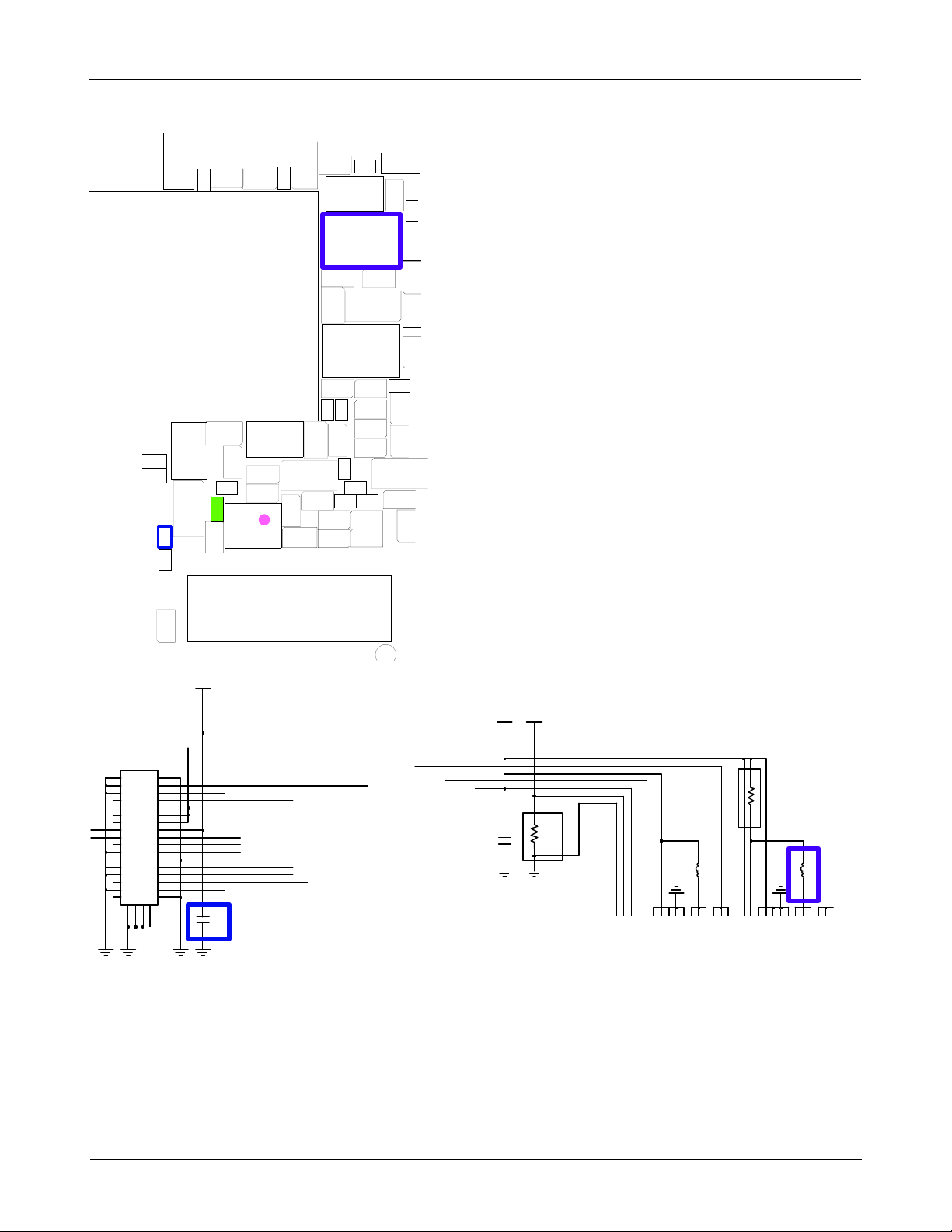
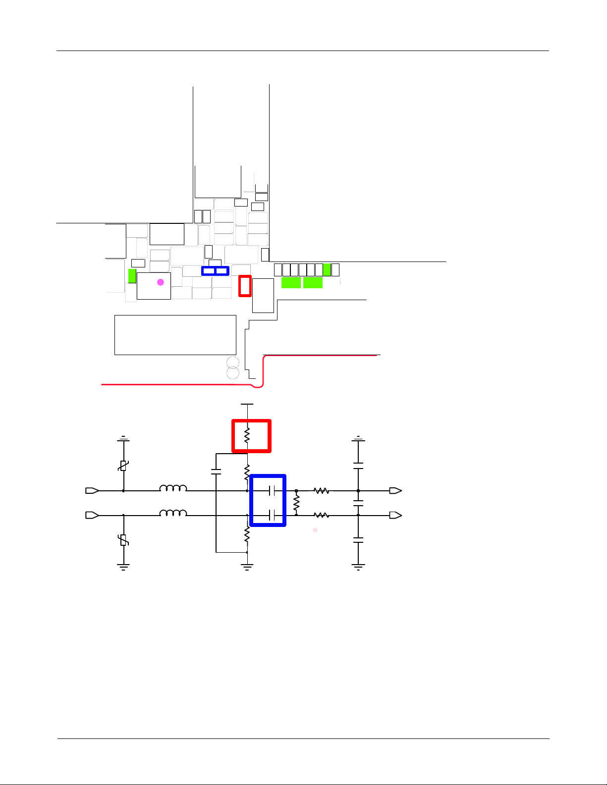
PCB Diagrams
8-2.
R240
U206
R
4
3
5
R
4
2
9
C
6
1
0
Top
TH400
C464
C352
C351
C353
C291
C294
C609
R
R
4
4
3
3
3
4
R
R
4
4
3
3
1
2
C336
C337
R
4
3
6
R
4
3
0
8-2-1.
H101
R
R
C
C
V
V
4
4
0
0
0
1
L
4
2
V
4
R
2
3
C248
8
C279
R
2
3
9
C250
C251
C256
O
S
C
2
0
1
C255
C262
C
R224
C278
2
6
5
L213 L215
C263
C264
R217
C267 C270
R306
R307
C
2
U207
9
3
C
2
9
6
L417
C462
L414
C461
C415
C
4
1
9
C427
L416
C
R
4
3
3
1
6
2
R
3
2
6
C471
TP_T_FLASH_CLK
C466
L
4
1
3
C498
R442
C
4
6
3
C425
L415
R486
C497
R
4
5
9
C493
H
D
C
3
0
0
R
3
1
5
R314
C
C
4
4
1
2
8
6
C416
C
C434
4
2
0
C
4
2
1
Q
E
R
_
K
L
C465
C
_
I
F
I
UME301
R344R345
R348
PAD100
R347
R342R343
R349
R346
W
C
C
C
3
4
4
6
3
7
0
9
2
U
3
0
0
C359
C367
R333
C368
C
R
3
3
7
3
3
5
C
C
3
3
7
7
1
2
C369
Z
R
C
D
3
3
C402
4
7
3
1
0
0
1
R111
C259
C266
C258
U204
C272
C
4
9
5
R504
R215
C
2
7
1
5
2
2
P
C273
T
C276C277
R
C
R
4
6
4
7
1
7
4
5
3
L
4
2
5
C
U406
6
1
3
C614
C292
C444
L
C
4
4
1
6
8
7
U403
C
4
L
3
8
4
1
2
R482
R481
C
4
6
0
C
6
0
4
R
4
7
6
C
4
8
6
C552
C
2
4
5
R334
C257
R
2
2
2
C240
C252
C517
C522
C518
Q
2
0
0
R500
C616
R475
L426
OSC400
C
4
7
L401
3
C459
L
4
1
1
C447
R
4
8
5
R
4
8
4
C524
1
L500
0
0
R
C513
3
0
8
R309
R480
TH401
R400
C484
L407
C437
C423
0
4
5
HDC400
0
5
0
5
R
4
1
2
U
4
L
V404
4
2
3
L
5
0
1
U
5
C523
R
5
0
6
C514
R
5
0
5
C502
U
C501
C515
R424
8
C410
0
R406
0
4
C
U
2
9
0
0
2
U
C443
R
4
1
5
C454
C468
0
2
4
U
C404
C413
C451
C445
R417
C414
L400
L409
C408
C
4
5
6
C457
L410
C475C476
C
C
4
4
7
7
0
8
C469
C
L
C403
4
4
0
4
6
8
C481
C
4
0
6
C492
R437
C494
C496
R465
L402L403
V400
V401
T
P
_
B
T
_
U
A
R
T
_
R
T
S
_
N
HDC501
F503 F504F506
D302
C
C
D301
C
4
4
6
C409
C
4
2
4
C
4
0
5
R428
D
X
T
_
T
R
A
U
_
T
B
_
P
T
C
C
3
3
3
4
4
4
3
2
4
5
1
R320
7
C
4
C417
5
5
C474
R
C328
4
2
3
C329
C458
C
4
C357
1
1
C356
C
3
C334
3
0
C363
C332
C
3
C331
3
3
C361
C322
R325
C477
C480
C479
C
3
2
0
C
C
C
C
3
3
3
3
0
2
2
2
7
4
5
R
4
2
5
7
R
C401
4
1
4
R403
BTC400
C289
C
4
8
2
C483
L
4
1
9
R
4
4
1
C449
C
4
5
0
C603
BH103
BH104
Y
B
T
S
_
M
A
C
_
M
5
_
P
T
C
C
3
3
0
2
6
6
C
5
1
6
C308
C340
UCP300
C
C
3
3
3
6
5
4
C510
M
A
C
_
M
5
_
T
S
R
_
P
T
C512
C
5
0
9
C
5
1
C
C
1
3
3
3
1
9
6
R
R312
R313
TP_VARM_FB
TP_VARM_NEGFB
R
3
3
1
1
C303
R323
1
0
C
R
C
R
C
3
3
3
3
3
0
1
0
4
5
4
8
5
9
0
C
4
0
0
D400
M
M
O
O
T
T
5
5
0
0
1
0
C
C
C
3
3
3
C354
C347
2
2
4
1
3
1
C355
C305
C311
C315
2
0
3
T
P
C
3
0
0
C302
C301
C362
C348
C346
C343
R411
C319
C318
C312
C310
K
L
C
X
_
B
S
U
_
P
T
C314
C
C
C
R
3
3
3
3
C313
2
0
3
5
2
9
8
8
BH1
8-2
Confidential and proprietary-the contents in this service guide subject to change without prior notice.
Distribution, transmission, or infringement of any content or data from this document without Samsung’swritten authorization is strictly prohibited.
Level3Repair
8-2-2.
H
K
4
0
0
T
P
_
L
C
D
_
C
S
X
T
P
_
L
C
D
_
R
E
S
X
TP_LCD_DET
TP_SYS_CLK_1
U
T
O
2
K
_
_
3
K
T
P
_
L
C
D
_
0
_
C
C527
Bottom
T
T
P
P
_
_
L
L
C
C
D
D
_
_
S
S
D
C
A
L
L
P
_
C
T
C532
C531
C526
U503
A
N
C
T
2
0
0
R
R
L
5
5
C542
D
5
0
4
R519
C
6
D
1
5
2
0
3
C546
V504
V503
C
R
R
R
5
5
5
5
3
1
0
1
0
1
3
2
T
P
_
L
C
D
_
0
H
D
C
5
0
2
R509
C534
C533
A
N
T
2
0
2
5
0
1
1
C544
4
5
3
L
5
0
2
C
5
4
5
C
5
4
7
C541
C287
L204
C
5
4
3
4
C
5
0
5
1
5
U
C
5
5
0
C
C
R
R
5
5
5
5
3
4
1
1
8
0
7
8
R510
U502
C528
C529
C
C
C
5
5
5
V
2
3
3
5
5
5
7
0
0
F
5
0
9
F
5
0
8
F
5
1
0
F
5
1
1
L
2
0
3
L218
C246
C238
C237
C244
L
C247
2
1
9
S
C283
C
1
0
2
L216
C433
C431
C
2
1
F
1
5
1
3
C216
C217
F
5
C205
1
2
L205
0
0
2
F
0
9
2
7
L
2
2
7
B
A
T
4
0
0
C485
SC101
C239
C280
5
0
C
C
L
C
2
2
2
2
2
8
5
5
0
2
3
4
C268
L
2
1
0
7
C269
0
2
U
C200
C
C611
6
0
6
R462
C
2
9
9
L
2
2
5
R487
Z
D
4
0
1
R
4
6
6
L
2
2
C288
L209
1
0
3
2
0
2
F
C219
C
2
4
1
2
U
C
2
4
3
C233
L
2
1
4
C234
C235
C
C230
2
8
4
L210
C
6
0
7
C
R
6
4
0
6
5
3
C601
R467
R469
L404
U
C
2
8
5
C
C
2
2
2
2
4
1
C
2
2
3
C213
C133
C507C508
F
5
0
7
F
5
0
5
C503
C506
C504 C505
F
I
7
_
0
P
1
T
C
S
TP202
C
2
1
4
C
2
0
7
C
1
3
L113
8
C139
C
1
5
8
C161
TP_CLK_T
TP_DAT_T
TP_SCLKTP_SDAT
TP_HVPRG
TP_RF_STROBE
TP_SYS_CLK_REQ
C
3
6
5
R
3
5
4
TP_MOT_PWM
0
0
M
A
C
_
T
V
_
5
T
S
R
_
P
T
C
D
H
Y
B
T
S
_
M
A
C
_
T
V
_
P
T
R
C
5
4
1
TP201
C452
C
1
4
0
C
C
1
1
0
1
4
7
C
1
1
3
C
1
1
1
C
1
2
2
C
1
1
9
C
4
1
2
0
4
3
2
C539
2
0
C
1
0
5
1
0
C
4
5
3
H
D
C
4
0
1
8
C
1
6
2
C156
1
L115
C
1
1
4
C
C440
D
D
C
4
4
4
4
0
0
1
2
3
C
1
0
S
L112
L109
C
1
L110
5
9
C132
C163
U
R
1
0
9
R110
C
C
1
1
6
5
0
7
C
1
5
5
C
R
1
1
2
0
0
5
L100
U
1
0
0
C
C
C
1
1
1
0
1
0
9
5
6
S
O
Q
1
0
0
C136
L
1
0
8
C
1
5
4
C144
R
R
1
1
R101
0
0
4
3
R102
C
1
1
8
R100
L
C112
1
0
2
C110
L
C123
1
0
3
C116
L
C125
1
0
4
C124
L
C131
1
0
7
C130
L
C127
1
0
5
C126
C121
C
C
1
1
L
0
0
C128
1
8
7
0
6
C129
L101
1
3
C
0
S
C145
C164
C151
C165
5
0
1
C
C146 C148
C171
P
A
M
1
0
1
S
L119
C
1
3
4
C
1
3
5
C
1
4
3
S
C
1
0
4
C167
L
1
1
8
C150
C
C166
1
4
1
C172
C
R
C
R
1
1
1
1
0
1
F
1
5
0
5
0
2
7
3
8
1
F
0
0
C
L
1
1
2
0
0
0
V
K
4
0
0
ANT101
R419
R420
L116
C
C
1
1
0
6
1
9
0
0
1
S
F
R
C215
1
0
R201
C
2
1
2
C208
O
S
C
2
0
2
L207
T
N
P
_
_
T
B
S
T
R
9
_
_
R
S
0
S
P
T
1
_
G
N
C
S
TP200
TP_U_TXD
T
P
_
U
R
_
3
R
5
X
3
D
T
P
_
W
I
F
I
_
S
D
TP_BT_VREG_EN
TP_WLAN_RST_N
I
O
_
C
L
K
L
2
1
1
C
L
2
2
C249
1
6
2
0
C274
R221
0
0
2
C
S
O
C261
C275
C
R
2
2
8
4
1
1
C
C
C
2
2
2
C232
3
3
4
1
6
2
C286
F
2
0
3
C228C229
C422
R
R457
4
C366
5
8
R355
L
C499
4
2
2
R330
C600
R329
C407
ZD402
C
R
6
4
0
6
C629
8
1
R328
R331
ZD400
R332
L
2
U
E
C209
D
5
0
0
F
L201
L222
2
0
2
2
C210
0
L
2
2
0
6
U
R202
R206
C201
L200
R207
L223
T
P
_
W
L
_
H
O
S
T
_
W
A
K
E
R200
L114
P
_
T
_
B
U
T
A
_
R
S
C
T
T
D
X
R
_
L111
T
R
A
U
_
T
B
_
P
T
R
2
2
5
R408
C430
C
4
3
6
R302
R303
C428
C435
R405
1
TP_IF_TXD
0
4
U
TP_SLE
R477
R478
C429
U301
TP_REF_OUT_EXT_2
TP_MC0_CLK
TP_REFOUTD_M
R356
6
0
1
C
S
8-3
Confidential and proprietary-the contents in this service guide subject to change without prior notice.
Distribution, transmission, or infringement of any content or data from this document without Samsung’swritten authorization is strictly prohibited.
Level3Repair
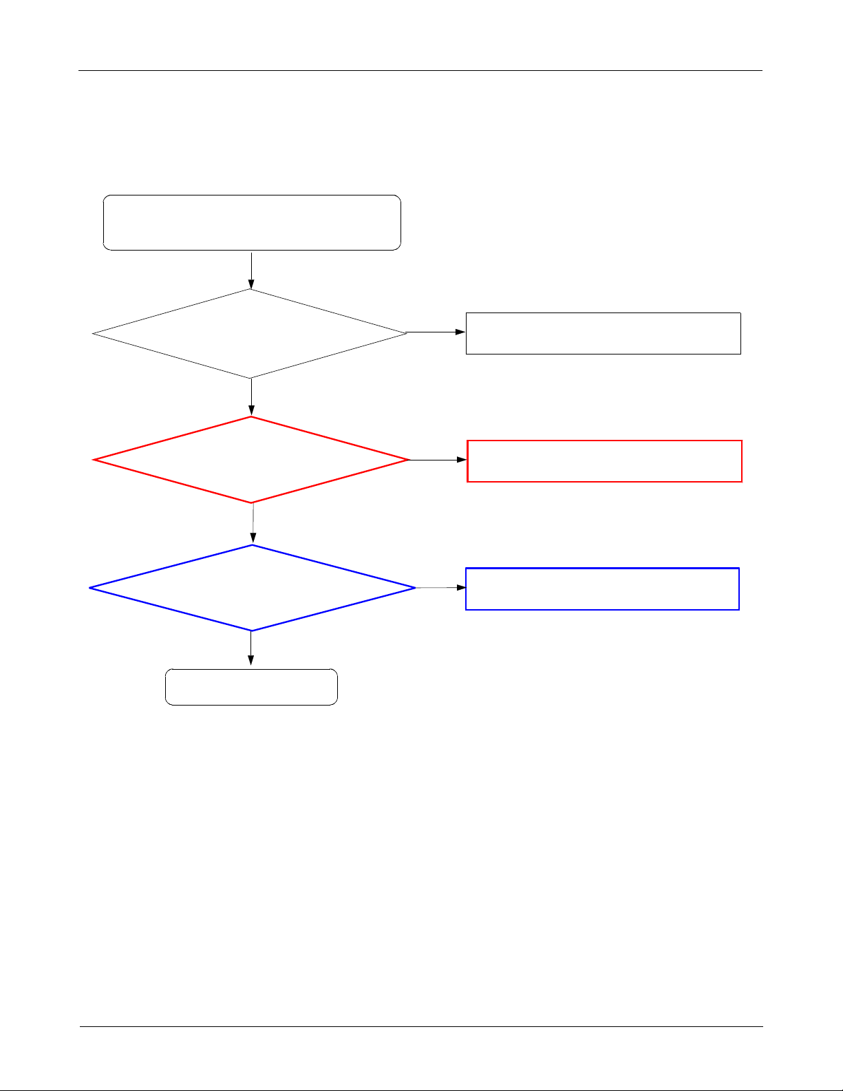
Flow Chart of Troubleshooting
8-3.
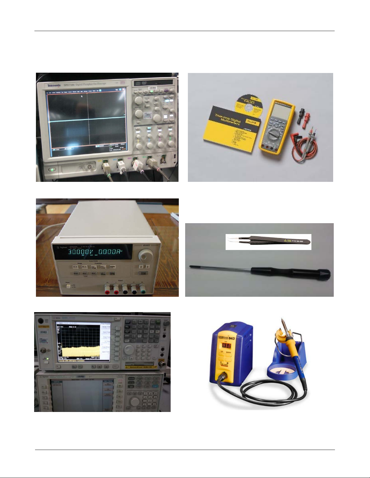
Equipments
Oscilloscope
Ç
Power Supply
Ç
Ç
Digital Multi-meter
Ç
driver, ESD Safe Tweezer
+
8960 &
Ç
Confidential and proprietary-the contents in this service guide subject to change without prior notice.
Distribution, transmission, or infringement of any content or data from this document without Samsung’swritten authorization is strictly prohibited.
Spectrum Analyzer
8-4
Soldering iron
Ç
Level3Repair
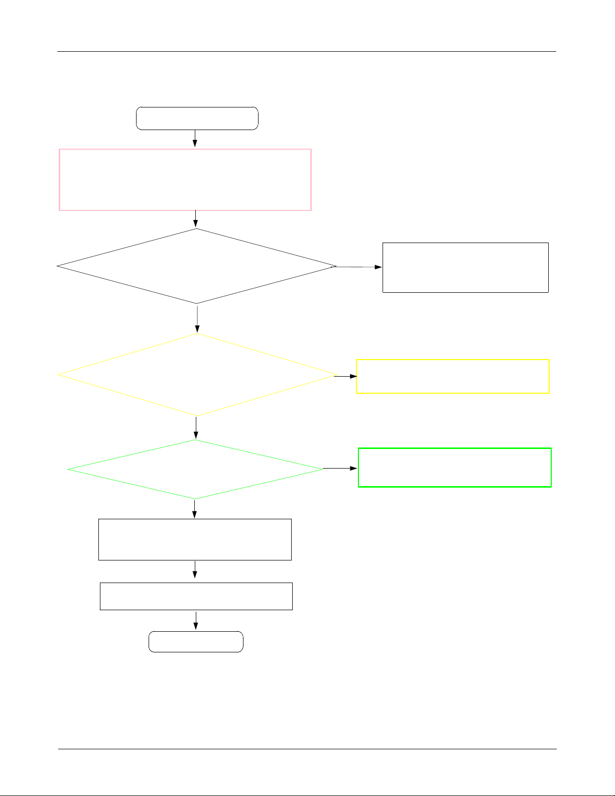
8-3-1.
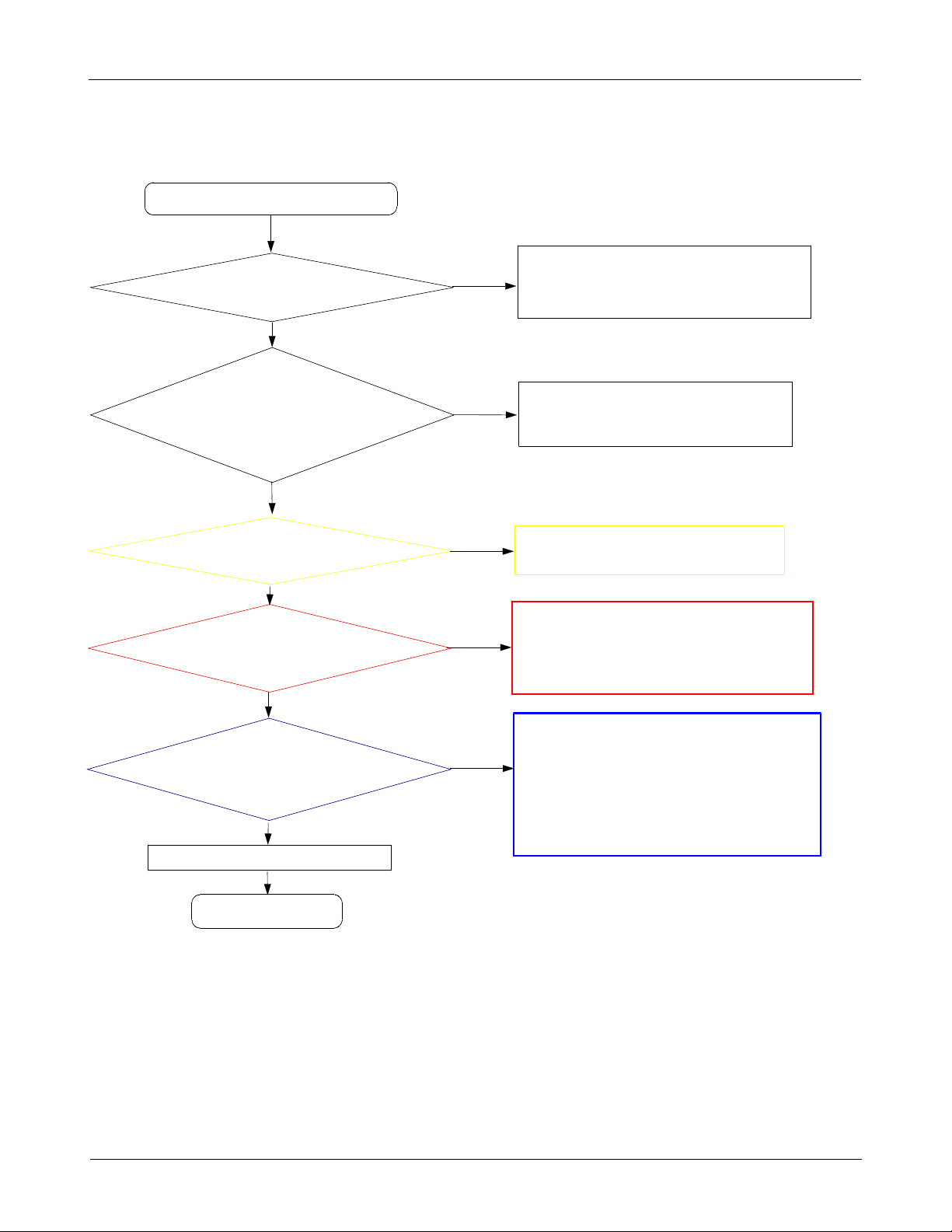
Power On
Mobile phone does not power on.
Check the Battery Voltage
it more than
Is
Yes
Power-on the phone and
check the power-on sound
or motor Vibration.
No
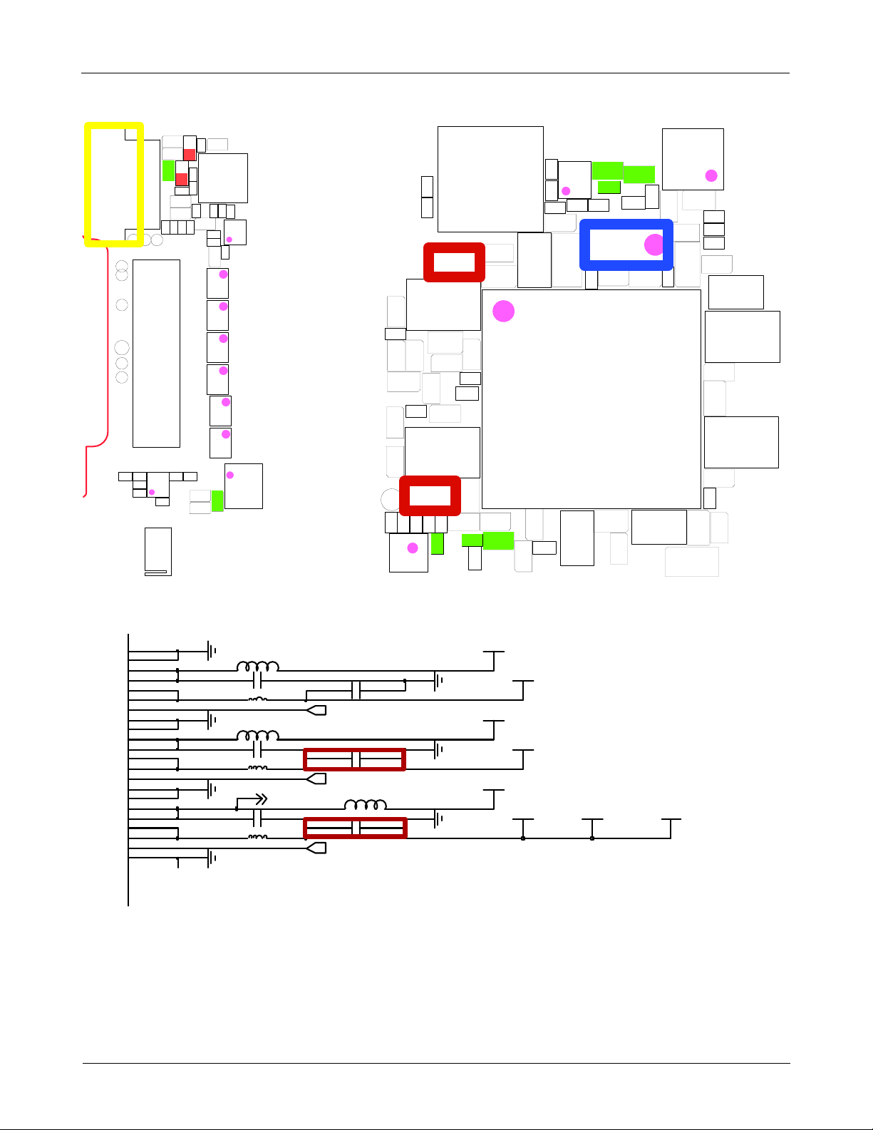
Check the HK400
soldering crack, open, etc)
(
3.5
V?
.
No
Yes
Abnormal
If its voltage level is extremely low(under
Change the FRONT-OCTA LCD ASSY
Change the HK400(Power-key FPCB)
Charging the battery by TA.
Change the battery.
And retry to the power-on operation.
3.0
V),
Yes
Check the U403 output voltage
C465
(
Check the Clock OSC400
Is that frequency
check the initial operation
>1.8
V, C462
Yes
Yes
Yes
END
>1.2
32.768
V)
Khz?
No
No
If the output voltage is not satisfied with normal
condition, Change the U403.
Each voltage level has
※
Change the OSC400.
If OSC400 does not still work, Change the U403
This problem is internal oscillator of U403.
Test condition(Oscilloscope setting)
※
us.div(time division)
:20.0
±10%
margin.
8-5
Confidential and proprietary-the contents in this service guide subject to change without prior notice.
Distribution, transmission, or infringement of any content or data from this document without Samsung’swritten authorization is strictly prohibited.
Level3Repair
V
H
K
4
0
0
T
T
T
P
P
P
_
_
_
L
L
L
C
C
C
D
D
_
D
_
S
S
_
D
C
0
A
L
T
P
_
L
C
D
_
C
S
X
T
P
_
L
C
D
_
R
E
S
X
TP_LCD_DET
H
D
C
TP_SYS_CLK_1
5
0
P
T
C
K
_
K
2
U
O
L
3
_
_
T
2
T
P
_
L
C
D
_
0
_
C
C527
C532
C531
U503
C526
C533
A
N
T
2
0
2
L
5
C542
D
0
C544
3
5
0
4
R519
C
6
D
L
1
5
5
2
0
3
C546
V504
V503
R
C
R
R
5
5
5
5
0
3
1
1
3
0
2
1
R509
C534
4
0
2
0
C
5
5
4
5
U
C
C
C
5
5
5
4
4
3
7
0
8
C541
U502
C528
C529
C
5
V
2
5
5
0
0
F
5
0
9
F
5
0
8
F
5
1
0
F
5
1
1
F
5
1
3
F
5
1
2
L
2
C287
0
3
L204
R
3
1
5
R314
C
4
1
8
C416
C
4
2
0
C
4
2
1
C
3
6
0
Q
E
R
_
K
L
C
_
I
F
I
W
C434
C
4
7
2
U
3
0
0
C
2
9
3
C
2
9
6
L414
C
4
2
6
C
4
1
9
L416
C465
C
R
4
3
3
1
9
6
C462
C461
C415
C427
C
4
3
2
R
3
2
6
U207
L
4
1
3
C498
R442
C
4
6
3
L415
R486
L417
C466
C425
C497
C
U406
6
1
3
C614
C292
C444
L
C
4
4
1
6
8
7
U403
C
4
L
3
4
8
1
R482
2
C
4
9
5
TH401
R475
L426
OSC400
C
4
7
L401
3
C459
L
4
1
1
R400
C484
R
4
1
2
L407
C
4
C410
8
2
C468
C404
C483
C413
L
4
1
C445
9
R
4
4
1
L409
C
4
5
6
C476
C
4
7
0
C
L
4
4
0
4
6
8
GNDVARM
GNDVARM
VINVMOD
VINVMOD
VMODLX
VMODLX
VMODFB
GNDVMOD
GNDVMOD
VINVSMPS1
VINVSMPS1
VSMPS1LX
VSMPS1LX
VSMPS1FB
GNDVSMPS1
GNDVSMPS1
VINVSMPS2
VINVSMPS2
VSMPS2LX
VSMPS2LX
VSMPS2FB
GNDVSMPS2
P19
AA11
Y11
AA10
Y10
Y12
AA9
Y9
B1
C1
A2
A3
B2
A4
B4
U1
V1
R1
T1
V2
R2
L411
L413
C459
L412
C461
L414
C463
CONNECT
C460
VMOD_FB
C462
VSMPS1_FB
L415
C465
VSMPS2_FB
8-6
VBAT
VBAT
VMOD
VSMPS1_1V2
VSMPS2_1V8
VSMPS2_1V8_VIN
SMPS2_1V8_RF
Confidential and proprietary-the contents in this service guide subject to change without prior notice.
Distribution, transmission, or infringement of any content or data from this document without Samsung’swritten authorization is strictly prohibited.
Level3Repair
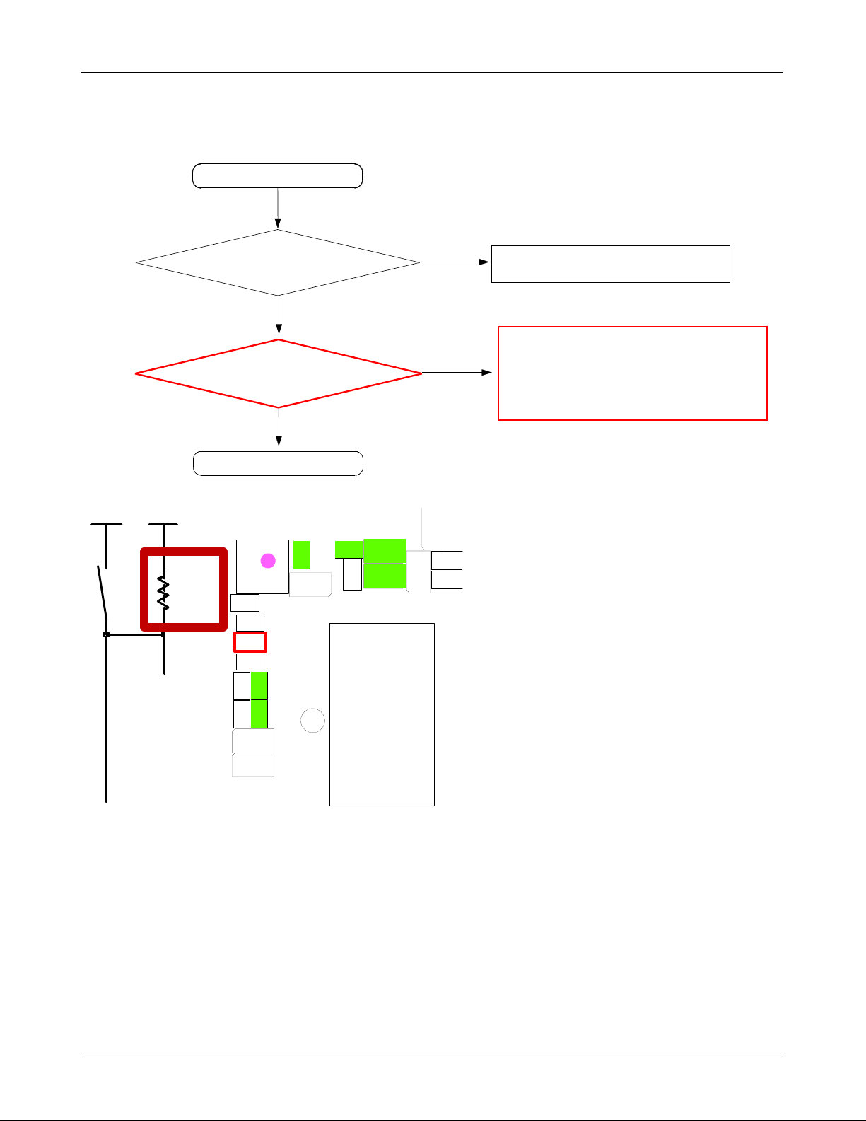
8-3-2.
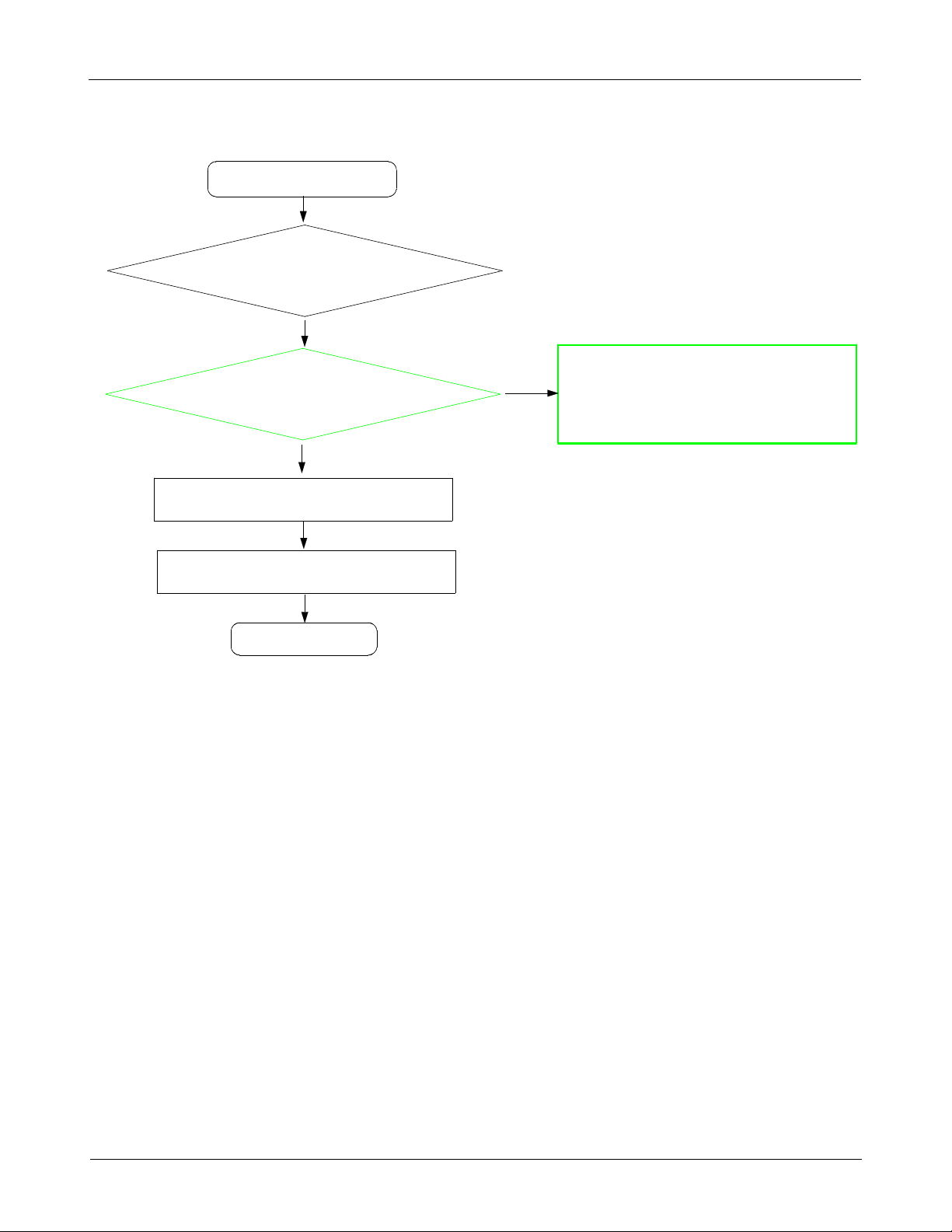
Initial
Initial Failure
Yes
Re-download latest SW on the
Check the oscillator clock waveform.
mobile phone.
Abnormal
KHz:OSC400,
32.768
MHz:OSC200
37.4
Normal
Change UCP300,U403
Abnormal
Change PBA
Abnormal
Check the OSC400, OSC200.
Crack, open etc.)
(
Check the output clock waveforms and frequency.
Test condition(Oscilloscope setting)
※
us.div(time division)
:20.0
END
8-7
Confidential and proprietary-the contents in this service guide subject to change without prior notice.
Distribution, transmission, or infringement of any content or data from this document without Samsung’swritten authorization is strictly prohibited.
Level3Repair
V
47nH1
RESET_TO_AB8500
PORN_FROM_AB8500
INTNDB8500
I2C_APE_SCL
I2C_APE_SDA
I2C_MODEM_SCL
I2C_MODEM_SDA
BAT_CTRL
CLK32KOUT1
WGBF_32K_CLOCK
1005
SMPS2_1V8
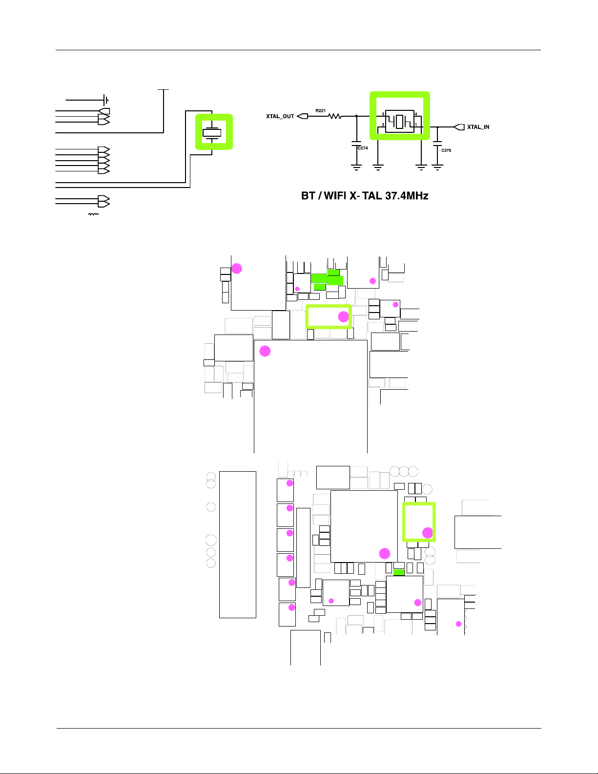
OSC400
CM315-32768-DZFT-K1S
32.768kHz
OSC200
C483
C239
C
2
9
0
2
0
U
8
C410
L
4
1
9
C468
C404
C413
C445
R
4
1
5
C414
C443
C454
0
2
4
U
D302
C451
D301
R417
C
4
4
6
L400
L409
C408
C
4
5
6
T
P
_
W
I
F
I
_
S
D
TP_BT_VREG_EN
TP_WLAN_RST_N
I
O
_
C
L
C
2
4
1
2
0
5
C
2
5
4
L
L
2
2
1
1
4
7
C
2
8
4
R487
K
L
2
1
1
C
L
T
P
_
2
2
W
C249
U
C
C
2
C232
4
2
2
4
3
C286
C233
C234
C235
C230
L210
C
6
0
7
C422
L
_
1
6
H
O
S
2
0
T
_
W
A
K
E
C274
R221
0
0
2
C
S
O
C261
C275
C
S
T
C
_
T
R
A
U
_
T
B
_
P
T
R
2
2
8
4
1
1
D
X
R
_
T
R
A
U
_
T
B
_
P
T
C
C
2
2
3
3
1
6
R
2
2
5
3
F
2
0
C
4
3
6
R302
C229
C228
R303
C428
C430
L114
L111
R408
1
0
4
U
TP_SDAT
R
R
C
4
6
7
1
4
R306
R307
C
2
U207
9
3
C
2
9
6
5
L
4
2
5
C
U406
6
1
3
C614
C292
3
0
R
8
4
7
3
R309
R500
R480
C616
TH401
R475
R
4
C
1
2
4
R400
L426
8
2
C444
L
C
4
L417
1
C466
8
V
5
0
0
F
5
0
9
F
5
0
8
F
5
1
0
F
5
1
1
C462
R
3
1
L414
5
R314
C
C
4
4
1
2
8
6
C416
T
P
_
L
C
D
_
C
S
X
T
P
_
L
C
D
_
R
E
S
X
TP_LCD_DET
TP_SYS_CLK_1
3
K
C
P
O
_
K
L
_
U
T
_
2
T
T
P
_
L
C
D
_
0
_
C
C
4
1
9
C461
C415
L
4
1
3
C498
R442
H
D
C
5
0
2
OSC400
4
6
7
C
4
7
L401
3
C484
R
4
4
1
U403
C
C
C
5
5
5
3
2
3
7
5
5
L218
C246
C238
C237
C244
L
C247
2
1
9
S
C283
C
1
0
2
L216
C433
C431
C
2
F
5
1
3
F
5
1
2
1
1
C216
C217
C205
L205
C280
C
C
L
2
2
2
2
8
5
0
2
3
C268
0
C269
0
2
U
C200
C
C611
6
0
6
R462
8-8
Confidential and proprietary-the contents in this service guide subject to change without prior notice.
Distribution, transmission, or infringement of any content or data from this document without Samsung’swritten authorization is strictly prohibited.
Level3Repair
8-3-3.
Check memu setting
Menu→applications→setting→wireless and network
mobile networks→network mode→setting is auto mode
No Service
Menu→Phone→Keypad
*#1234#
Check the C100, C172, L118 is well
No service
Yes
check Phone version
→
PHONE:I9070XXXX
No
soldered
→
→
→
?
PHONE:I9070XXXX
No
Check the connection of RF coaxial cable
on RFS100
(
Re-solder C100, C172, L118 correspondingly.
)
Yes
Check VREF
VREF(R110)
Change the Intenna
Change the board
=1.2V
Abnormal
Abnormal
Yes
END
No
Replace the U102
8-9
Confidential and proprietary-the contents in this service guide subject to change without prior notice.
Distribution, transmission, or infringement of any content or data from this document without Samsung’swritten authorization is strictly prohibited.
Level3Repair
C
1
3
L113
8
C133
L114
C139
C
1
5
8
L111
C161
C
1
1
7
C
1
1
3
TP_CLK_T
C
1
1
1
C
1
2
2
C
1
1
9
C
4
1
2
S
0
C
8
1
C
1
6
2
L112
C156
L109
C
1
L110
5
9
C132
C163
U
1
0
2
R
1
0
9
R110
C
C
L
1
1
1
0
5
6
8
7
C
1
4
0
C
1
0
4
0
C
C
1
5
1
4
5
5
L115
C
C
C
1
1
0
1
5
4
R
R
1
1
1
2
0
0
0
4
5
L100
U
1
0
0
C144
R
1
R101
0
R102
3
C
1
1
8
R100
L
C112
1
0
2
C110
L
C123
1
0
3
C116
L
C125
1
0
4
C124
L
C131
1
0
7
C130
L
C127
1
0
5
C126
L
C128
1
0
6
C129
1
0
1
F
5
0
1
C
S
C167
L
1
1
8
C150
R
1
0
7
S
C
1
0
4
ANT101
R419
C
C166
1
4
1
C172
C
R
C
1
1
1
0
5
5
2
8
3
F
0
0
1
C
L
1
1
2
0
0
0
R420
L116
C
C
1
1
0
6
1
9
0
0
1
S
F
R
ANT101
3
G
RFS100
G
G
C
A
4
2
1
3
4
1
I
N
F
R
G
G
2
C101
C169 L120L116
C100
C172
6
6
1
C
L118
7
6
1
C
RF_OUT_HB
1
4
1
C
RF_OUT_LB
0
5
1
C
VREF_1V2
3
6
1
C
R110
8-10
Confidential and proprietary-the contents in this service guide subject to change without prior notice.
Distribution, transmission, or infringement of any content or data from this document without Samsung’swritten authorization is strictly prohibited.
Level3Repair
8-3-4.
NFC_VSIM
Sim Part
CP_VSIM
Insert SIM card
Yes
Is SIM/SD assy well
connected to main board?
Yes
Check the SIM Voltage.
R333)
(
>= 1.8or3.0?
Yes
END
No
No
Reassemble SIM/SD assy and still SIM
does not work, replace SIM/SD assy
Change to the new SIM card.
If it doesn`t still work SIM card after changeing
the SIM card, Check the UCP300(Crack etc)
R334
R333
C359
C367
R333
C368
C
3
7
3
C
3
7
1
C369
C402
R
3
2
6
TP_T_FLASH_CLK
R486
C497
C
R
4
5
9
C493
R482
4
9
5
R481
H
D
C
3
0
U
3
0
0
C471
R
3
3
5
C
3
7
2
0
8-11
Confidential and proprietary-the contents in this service guide subject to change without prior notice.
Distribution, transmission, or infringement of any content or data from this document without Samsung’swritten authorization is strictly prohibited.
Level3Repair
8-3-5.
Charging Part
TA/USB Insert
Charging Sequence Start
Is Touch key FPCB well
connected to main board?
Battery is Charging?
C604
Yes
=5V
Yes
Yes
Yes
No
No
Reassemble touch key FPCB and if still does
not work, try with new touch key FPCB
No
Reconnect TA or USB
Resolder or Replace L400
END
8-12
Confidential and proprietary-the contents in this service guide subject to change without prior notice.
Distribution, transmission, or infringement of any content or data from this document without Samsung’swritten authorization is strictly prohibited.
Level3Repair
R482
R481
C
6
0
4
R
4
7
6
C
4
6
7
U403
L
4
1
2
C
4
6
0
C
4
7
3
L401
C459
C447
R
4
8
5
R
4
8
4
L
4
1
C445
C
C414
L400
L409
C
4
5
6
L410
C
C
4
4
7
7
0
8
L
4
0
6
C496
V401
C
4
0
6
R437
R417
C408
C457
C475C476
C469
C403
C481
C494
L402L403
V400
C
4
4
6
C409
C
4
2
4
C
4
0
5
C492
R428
R
4
2
3
C
4
1
1
C
3
3
0
C
3
3
3
R
4
2
5
9
R
4
4
1
C484
4
4
L407
L
4
1
1
C437
C423
4
0
5
8
C449
C
R465
4
5
0
U
C603
HDC400
11
55 66
778 8
99
10 10
11 11 12 12
13 14
13
15 16
15
17 18
17
19
20
19
212122
232324
252526
27 28
27
293330
29
313132
333334
NC
NC
NCNC
3738
35
36
C
4
8
6
VBUS
22
4
4
14
16
18
20
22
24
26
28
30
32
34
C604
HDC400
D
X
T
_
T
R
A
U
_
T
B
_
P
T
BGND_P
VBAT
3
2
4
R414
1
1
4
C
9
1
4
L
R
0
0
4
L
8-13
Confidential and proprietary-the contents in this service guide subject to change without prior notice.
Distribution, transmission, or infringement of any content or data from this document without Samsung’swritten authorization is strictly prohibited.
Level3Repair
8-3-6.
Microphone Part
Check microphone function
in voice call receiver mode
or in Voice Recording mode
Check touch key FPCB where
main MIC is placed
for any damage(Tear in FPC,
Check the voltage at
etc)
R425
Yes
Yes
=2.1V
No
No
Change the touch key FPCB
Resolder or replace R425
Yes
Check component soldering
statuses of C494, C496
Yes
END
No
Resolder or replace C494, C496
8-14
Confidential and proprietary-the contents in this service guide subject to change without prior notice.
Distribution, transmission, or infringement of any content or data from this document without Samsung’swritten authorization is strictly prohibited.
Level3Repair
C322
C409
C475C476
C
C
4
4
7
7
0
8
V401
C469
L
C403
4
0
6
C481
C
4
0
6
R437
C494
C496
L402L403
V400
L
C459
4
1
2
C
4
6
0
L407
L
4
1
1
C437
C447
C423
R
4
8
5
4
0
5
R
4
8
4
C
4
4
8
C449
C
R465
4
5
0
U
C603
C
4
2
4
C
4
0
5
C492
R428
R325
C477
C480
C479
C
3
2
0
C
3
0
R
4
2
5
7
R
4
1
4
C
3
2
4
C401
C
C
C
3
3
2
2
5
7
C
C
C
3
3
3
3
2
3
0
6
6
6
4
5
R403
MIC2N_CON
0
0
4
V
1
0
4
V
HDC400
L402
L403
D
X
T
_
T
R
A
U
_
T
B
_
P
T
T
P
_
B
T
_
U
A
R
T
_
R
T
S
_
N
VAMIC2_2V1
C492
BTC400
R425
5
0
0
1
R428
C493
C497
C495
MIC2PMIC2P_CON
MIC2N
R465
C494
C496
R481
R437
R482
8-15
Confidential and proprietary-the contents in this service guide subject to change without prior notice.
Distribution, transmission, or infringement of any content or data from this document without Samsung’swritten authorization is strictly prohibited.
 Loading...