

Page 1
Level
8.
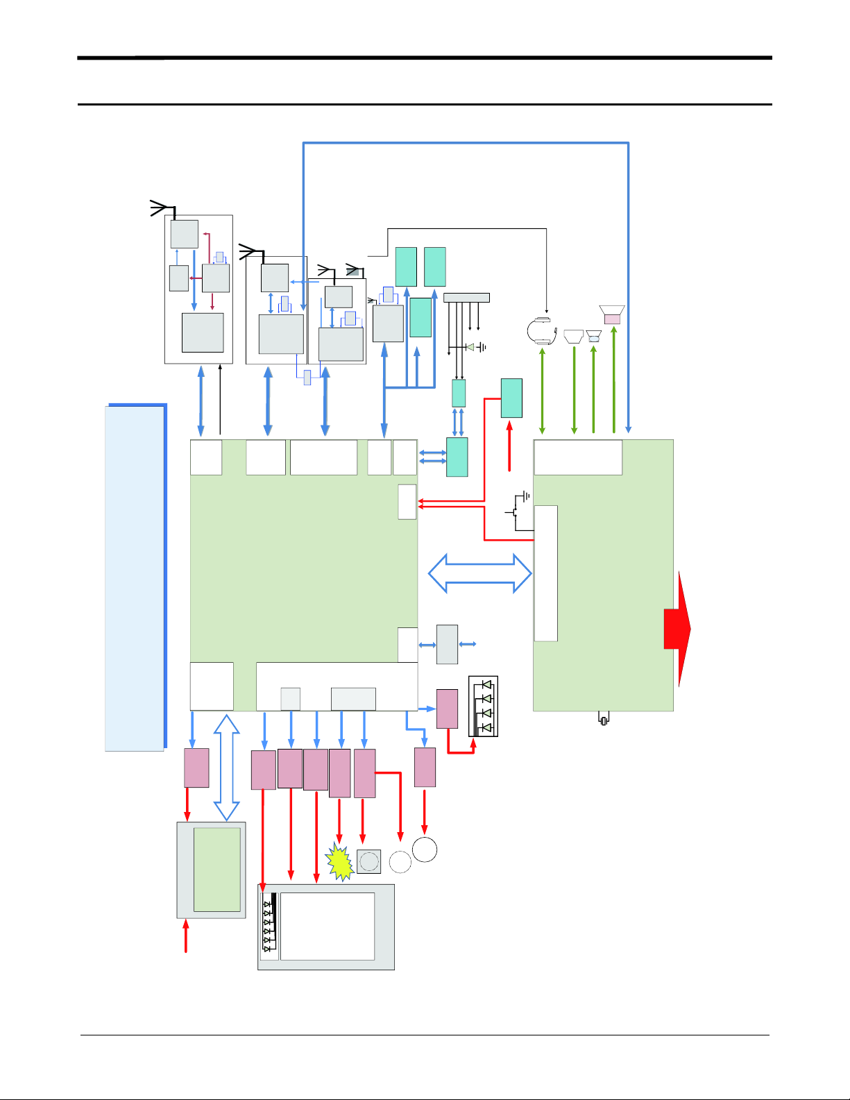
Block Diagram
8-1.
Repair
3
FEMid
RFMD
RF1292
DCXO
26MHz
PAM
RF6277
STE
RFMD
PM3535
PMU RF
STE
TRCV
RF3500
RF BLOCK
Updat ed Date : 2012.10.20
SYS_CLK_REQ /
RX_DA,TX_DA
RF_STOBE / SCLK / SDAT
RF BB IF
ANT
BT /WIFI
FM ANT
WIFI ANT
AWL9565
OSC
34.7MHz
STE
WIFI
CW1250
WIFI
BT_UART_TXD
BT_UART_R TS
BT_PCM_CLK
BT_PCM_SY NC
BT_PCM_DI
BT_UART_R XD
BT_UART_C TS
BT_PCM_DO
SDIO
UART
GPS ANT
TCXO
GBF_BT_RF
S/W
GPS/BT
MGF7301
STE
CG2905
GPS/BT/FM
BT/ GPS/ FM BLOCK
26MHz
UART
27MHz
OSC
26MHz
STE
NFC
PN547
I2C
STE
AP + CP
DB8520H
TAOS
ACCEL
BOSCH
BMA254
TMD2672
Proxi Sensor
ALPS
VBUS
COMPASS
HSCDTD006
I2C
DP DM
TSU6111RSVR
PORN
Micr o USB CON
USB_ID
V_BAT_FET
PTVS26V
ACRE1A2G90E
TI
u-USBSW IC
RESET IC
FT7521L6X
Phone R esetPhoneReset
Power o n KEY
EARPHONE
MIC
3PI_ADC
MIC2P / N
3PI_DETECT
Fairchild
EAR_MIC_P / N
EAR_SPK_L / R
AUDIO
FM_I2S_DO
FM_I2S_CLK
FM_I2S_SYNC
FM_I2S_DI
SPK
RECIEVER
SPK_P / SPK_N
RCV_P / RCV_N
AMP
STE
AB8500
System control IF
(BB / PMU)
MC0
((TTII))
LLeevveell SShhiifftteerr
TTXXSS00220066--2299
Main Power Supply
GGOOLLDDEENN BBlloocckk DDiiaaggrraamm HH//WW RREEVV00..77
MC2
RICOH
VVMMEEMM__33VV33
RP114K331D-TR
EELLVVDDDD__44..66VV
STOD13AMTPUR
MC2_DAT_[0: 7]
VMEM_3V3
LCD BACKLIGHT
((SSAANN DDIISSKK))
SSDDIINN77DDUU22--88GG--994444LL
ii NNAANNDD((88GG))--eeMMMMCC 44..4411
PHONE MEMORY
VSMPS2_1V8
GPIO
MIPI
DSI0
RICOH
EELLVVSSSS__--44..99VV
RP152L010B-TR
VVRREEGG__LLCCDD__33..00VV
VVRREEGG__LLCCDD__11..88VV
AMOLED LCD
MIPI
CSI0
CSI1
RICOH
SM5103
KINETIC
MIC5365-1.8YMT
TTOOUUCCHH__KKEEYY__11..88VV
OCTA TSP
LCD
MAIN LCD
4.0", AMOLED
SILICONMITUS
KTD262EJH-TR
CCAAMM DDCCDDCC//LLDDOO
FFLLAASSHH LLEEDD DDrr IICC
CAM
FLASH
VGA
CAMERA
CAMERA
5Mega AF
(OCTA)
OCTA TSP MOD ULE
MICREL
KKEEYY__LLEEDD__33..33VV
MIC5365-3.3YMT
KEY LED 3.3V
MICREL
LLDDOO__33..33VV
MIC5365-3.3YMT
32.768kHz
M
LINEAR MOTOR
8-1
Confidential and proprietary-the contents in this service guide subject to change without prior notice.
Distribution, transmission, or infringement of any content or data from this document without Samsung’swritten authorization is strictly prohibited.
Page 2

Level3Repair
B
B
8
9
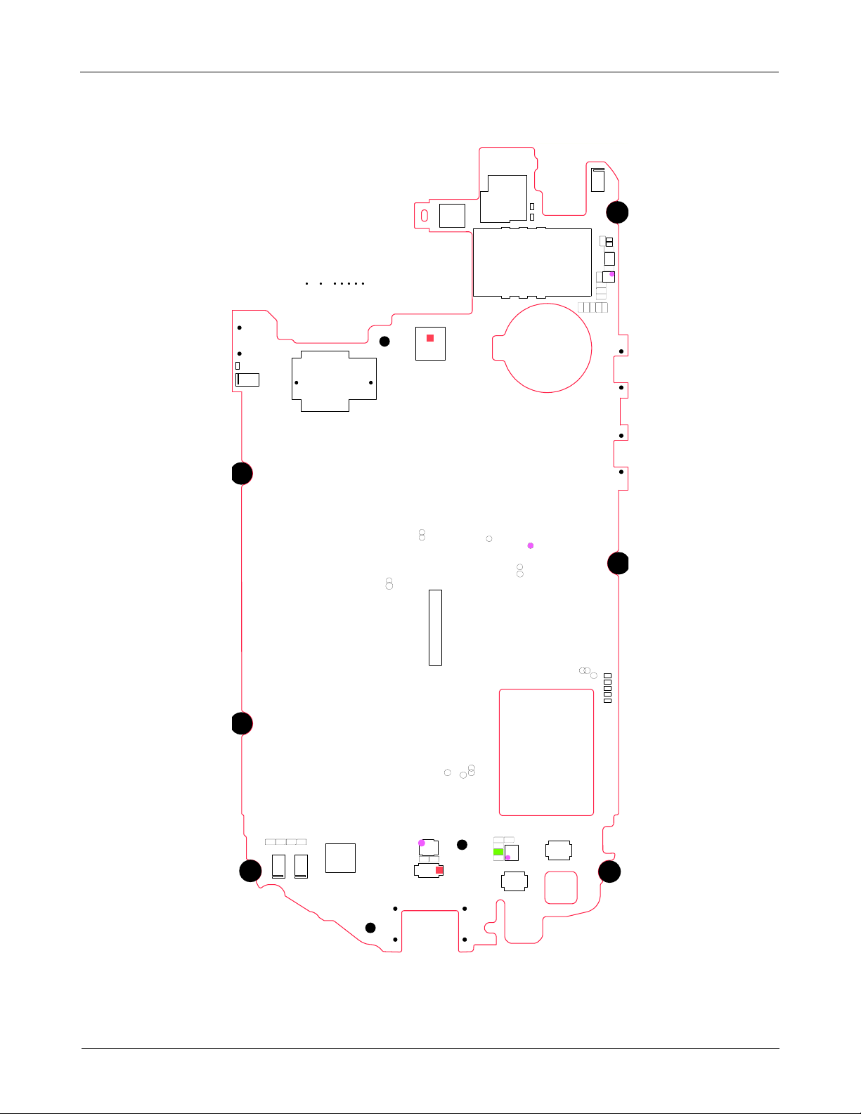
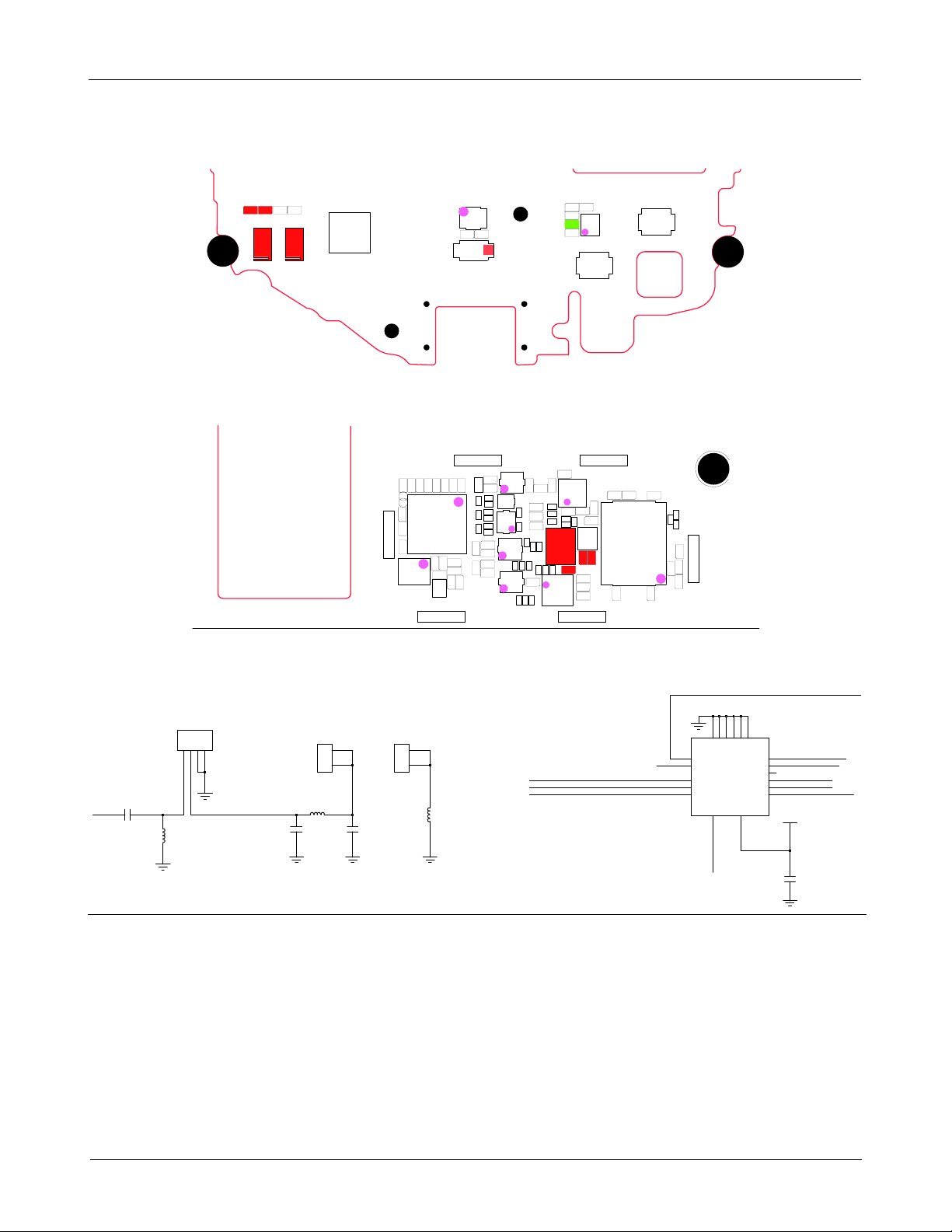
PCB Diagrams
8-2.
8-2-1.
Top
OTHHOLE102
U205
L
5
7
5
7
7
C
2
4
1
5
C
L
5
1
ZD510
5
D
Z
0
2
8
Z
7
D
L
1
5
5
8
5
0
2
4
L
2
3
5
T
P
_
V
T
_
R
E
S
E
T
0
0
S
L
5
C
T
P
_
V
T
_
S
T
B
Y
R
L
5
5
1
2
L
5
1
3
1
0
C517
L
5
0
2
F501
F503
C290
R
2
0
8
C569
5
5
3
R
C561
C518
ZD507
L514
C
2
2
5
6
0
C
6
C559
L515
R
5
4
9
5
4
4
R
5
7
0
C
G
B
T
N
I
P
_
T
P
_
P
T
2
0
4
R
C
C
C
C211
R203
C231
4
4
4
3
0
1
7
0
1
5
D
Z
0
4
C
4
6
ZD505
1
1
0
5
C
5
7
8
C
C579
1
C
0
4
0
5
4
U
R
C409
3
7
1
1
2
4
R
C
C
4
0
8
0
0
4
L
0
6
C
4
3
1
1
R
3
D
1
A
0
R
3
2
4
P
OTHHOLE101
BOTHHOLE103
BOTHHOLE107
T
A
C
T
5
0
1
C566
C
5
L
C568
T
A
C
T
5
0
2
P
T
U
O
_
B
I
V
_
P
T
N
T
U
O
_
B
I
V
_
P
T
9
2
1
2
2
6
0
5
0
4
C
0
0
2
0
1
2
R
C
2
3
0
9
2
2
C
2
1
2
C
TP_NFC_CLK_REQ
TP_FM_I203
R
C
C
R
R
5
4
4
5
5
2
2
6
1
2
1
3
5
9
0
5
1
2
7
4
4
C
C
C426
C
C
4
4
5
4
3
4
9
4
9
4
8
3
3
4
C
4
C
R
C476
3
1
4
7
2
8
6
4
C
C486
C
4
7
0
0
0
L
4
4
0
9
C
C
4
4
S
0
O
C
4
6
6
3
3
4
C493
C
C
4
C
C
7
2
4
4
6
6
2
1
4
9
9
C
C482
Y
D
R
D
_
S
C
2
2
5
S
A
P
M
O
C
_
P
T
9
0
2
4
2
2
C
U
R
R
3
3
6
2
2
5
8
9
5
C
F200
OSC200
U
2
0
2
TP_FM_I202
TP_FM_I200
C469
4
6
7
C
L
4
C
C473
C474
C
4
1
7
3
2
2
2
L
C
C
1
0
2
L
2
1
5
C
U
R205
2
T
P
6
0
0
2
2
0
7
P
T
3
T
P
2
0
200
5
T
P
2
0
TP200
4
2
3
2
C
C
2
0
2
C219
L207
R206
4
6
6
C
3
6
5
C
R
C455
5
4
7
C
5
5
C
8
4
3
1
4
4
0
0
4
4
5
3
4
0
C
4
L
L
C
5
6
4
R542
5
8
0
3
C
4
4
C
C550
U
4
0
6
C
4
1
5
L
L
4
4
1
0
0
L
4
8
0
7
6
1
C
8
4
1
4
C
R
4
8
2
1
0
1
3
4
4
R
R
C
4
3
5
8
6
5
5
4
4
R
C
C
4
5
9
2
1
1
0
4
4
T
P
R
_
R
G
N
D
_
D
E
T
_
A
B
4
0
0
C
2
7
2
2
2
3
C
4
0
2
R
3
1
4
U
R
3
1
5
C
2
7
3
C274
1
0
0
0
4
4
T
T
O
O
M
M
C510
0
0
5
L
0
0
5
U
C530
6
9
7
1
8
0
0
0
0
1
5
5
5
5
5
R
R
R
R
R526
C
T
P
_
I
F
_
R
X
D
C562
4
0
2
C
9
5
C
C
T
4
P
4
4
_
I
6
9
F
C
_
0
5
T
X
D
4
8
1
C
C
4
R
3
C
C
C
C
1
4
4
4
4
4
2
2
8
9
2
2
8
4
8
9
4
C
C
4
9
4
C549
C
4
6
1
2
3
L412
0
C
C
C
3
3
1
1
8
9
C
4
3
8
L401
C
3
1
0
C
4
0
1
C400
C375
C302
L402
C450
4
7
7
C
C
4
5
2
C451
4
3
4
C
T
P
_
P
L
O
R
N
4
9
T
8
P
0
_
R
E
4
S
6
E
T
C
4
1
4
C421
C
TP_BT_VREG_ON
C
4
2
3
4
4
3
4
1
C
4
C
4
4
3
L
0
0
4
7
2
H
T
5
9
4
4
C
C
S
E
R
C370
V
I
C
E
_
A
B
8
5
0
5
3
3
5
R
C
3
6
3
U306
T
P
C
3
6
2
3
0
C369
0
TP303
TP309
R
3
4
1
R340
U308
C368
5
0
3
7
P
6
T
3
C
4
0
1
C
S
C527
R
3
1
7
C
3
1
1
2
1
3
C
0
2
C
4
5
4
T
P
_
3
0
1
2
5
3
C
P
3
0
7
6
6
3
C
BOTHHOLE110
T
P
_
5
M
_
S
T
B
Y
0
1
S
L
5
C
T
P
_
5
M
_
R
E
S
E
T
D
4
0
0
C
4
8
8
3
3
3
5
0
C
5
L
U
5
0
3
L
5
0
4
C531
TP_BT_PCM_SYNC
TP_BT_UART_CTD
TP_BT_UART_RXD
2
1
5
R
TP_BT_UART_TXD
C324
R
3
1
6
C325
C348
C
3
1
5
3
1
3
C
TP_BT_UART_RTS
5
0
R
5
0
C
3
7
3
C
C
7
3
1
7
3
4
C
3
5
6
C
C
4
8
3
C
4
7
5
C464
3
1
9
R
R
3
0
0
5
9
0
2
3
3
C
C
T
Q
N
E
_
R
T
_
S
K
R
L
_
C
TP_WLAN_SDIO_DATA2
N
_
A
S
L
Y
S
W
_
_
P
P
T
T
2
1
6
2
2
0
1
1
1
L
C
C
T
_
T
A
D
_
P
T
T
_
K
L
C
_
P
T
8
1
1
C
C
1
0
7
C
1
0
6
0
0
1
C
S
C504
9
0
5
L
1
0
1
1
5
5
C551
L
L
C
1
5
0
0
3
5
D
Z
5
0
1
5
1
5
C
F500
F502
F504
4
1
5
C
C532
5
0
5
6
L
0
5
L
C535
C536
9
8
2
2
5
5
C
C
TP_BT_PCM_CLK OD_MCP_TB_PTID_MCP_TB_PT
T
T
P
P
2
2
2
2
9
8
5
1
6
R
0
C478
0
5
R517
R
4
2
9
Q
R
3
2
7
C
3
2
3
C
C
C
C
C
C
C
C
3
3
3
3
3
3
3
3
5
4
4
2
0
2
6
0
7
3
2
0
6
6
5
7
U
C
P
3
0
0
5
2
3
8
4
0
4
3
2
R
0
4
6
6
1
3
3
3
3
3
1
3
C
C
C
C
R
C
U
M
E
3
0
1
E
K
A
W
TP_WLAN_SDIO_CMDTP_WLAN_SDIO_DATA0
TP_RF_STROBE
_
T
B
_
P
T
S
C
1
0
5
0
4
2
0
9
5
4
4
2
2
1
0
0
0
1
1
1
1
1
1
L
0
2
C
C
C
R
C
7
3
1
8
2
1
L
9
3
1
C
U
3
4
1
C
L
1
3
3
8
4
1
C
1
0
1
4
1
C
L
1
3
0
0
2
4
1
C
C100
3
0
1
L
C101
C
C
1
1
5
1
3
1
0
3
1
C134
L
C
1
O
1
0
C
1
1
7
C136
C116
L
1
4
0
1
5
1
C
Q
0
1
0
C
S
1
0
6
C
C
5
5
ZD401
2
2
5
6
R
5
5
9
2
U
0
5
8
F
5
0
R
5
5
8
C
C
2
4
5
5
3
3
4
4
5
5
0
1
R
R
R536
C
4
9
1
U404
7
8
4
C
R436
5
1
2
C
5
1
3
C
R561
H
L
C534
D
F
C
5
0
5
5
0
0
F
5
0
6
L507
L508
F
5
0
7
2
3
4
R
6
7
2
C
1
3
0
0
4
C
4
8
0
2
C
4
6
2
U
2
0
4
U
4
3
3
C
L
1
L
1
C
5
6
6
2
2
5
C
C
Q
C
4
7
9
6
4
7
3
4
5
3
C
7
4
L
2
1
2
C
2
3
2
C
R
C
C
C
3
3
3
3
5
7
2
6
0
C
C
C
C
5
0
1
3
3
3
4
4
3
1
0
7
2
6
8
C
C255
U207
R232
3
7
3
0
2
3
2
2
4
R
R
1
0
2
R
0
2
3
R
9
4
3
C
1
5
3
C
1
3
0
R
9
0
3
R
C
3
3
3
C
3
7
2
R326
C
3
2
1
C
3
3
9
C
3
5
9
3
5
8
C
2
7
8
0
1
C
3
3
6
2
2
2
3
3
3
3
3
3
3
C
C
C
C
C
3
3
8
C
8
0
0
1
3
3
P
P
T
T
0
0
3
B
D
N
T
N
I
_
P
T
C361
R332
R331
R334
R305
R304
R333
R330
R308
R303
R306
C
3
5
4
1
3
1
L
L
1
1
F106
2
2
5
6
L121
7
0
F
1
L
1
2
4
L120
7
4
C160
1
L
C130
1
3
5
C
C182
8
9
1
1
L
0
0
0
1
1
6
L123
4
1
F
L
8
0
1
1
L
L
1
2
0
0
0
7
1
C
1
F100
F
C
L
1
1
5
1
2
1
6
3
1
L
C
L
1
1
2
1
1
1
3
2
1
L
C
1
2
7
F102
F103
C
L
1
1
7
1
2
1
8
8
1
L
C
5
C
4
9
6
6
5
L
4
1
5
0
5
4
R
ZD400
C
4
9
7
C249
C
C
1
9
2
2
3
4
5
4
6
6
2
2
2
4
2
C
C
C
9
1
L211
2
R
C240
C
2
6
1
C267
C269
2
4
6
C
R
C262
8
R
5
6
0
1
2
R
8
3
2
C
C210
TP_HOST_WAKE
C296
2
4
2
5
5
5
U
R
9
9
2
C
L209
C245
O
S
C
R
2
2
0
7
R
2
4
3
0
1
C
C
2
2
8
4
2
4
R230
C
1
6
5
L111
0
0
1
C
S
C
C
1
7
9
1
7
5
L
1
C176
3
1
4
3
4
7
1
1
C
C
C
S
1
0
1
0
7
S
C
1
C
5
0
1
5
4
C
C151
1
F
C
1
5
9
L
1
3
7
1
C172
0
1
L
L
4
1
0
0
0
1
F
L
1
8
0
0
9
1
C
C
1
2
9
C157
L
1
4
1
2
5
1
C
C146
S
C
1
0
8
0
C243
6
3
2
C
U101
4
2
R
F203
1
5
2
C
9
3
TACT500
BOTHHOLE10
L
2
7
6
4
1
8
8
1
6
2
2
2
L
C
C
2
0
2
F
C
2
2
1
5
4
8
2
5
2
C
9
3
3
3
3
2
2
2
2
C
C
R
R
C
C
4
2
2
1
1
1
2
7
8
3
5
2
C
C
U201
C297
L206
7
4
2
C
C
C298
2
0
4
5
8
2
C
C
2
1
2
2
8
8
2
2
5
C
C
2
4
9
C
2
C
7
2
2
C
8
7
2
1
2
2
C
L
8
8
2
C
C
2
C
7
2
9
8
0
0
7
2
C
L
2
1
5
8
7
2
C
1
7
2
U
C
8
0
2
L
2
2
5
6
C
0
C
2
7
7
8
C275
5
0
2
C
R
8
2
7
C
5
3
3
2
2
6
2
C
C
5
L
2
1
0
7
TP_WLAN_SDIO_DATA1
TP_WLAN_SDIO_DATA3
1
0
2
S
C
C
8
1
7
L135
2
4
1
L
C
1
6
4
1
1
2
R
2
6
1
C
C
1
8
0
S
C
1
0
3
L
1
3
L
1
4
0
9
BOTHHOLE10
1
5
0
C
9
6
1
C
7
6
1
C
C
1
6
6
A
P
M
6
5
1
C
S
C
1
0
9
1
6
8
1
3
C
1
L
8
5
1
C
3
5
1
C
BOTHHOLE104
MIC500
IFC500
BOTHHOLE106
8-2
Confidential and proprietary-the contents in this service guide subject to change without prior notice.
Distribution, transmission, or infringement of any content or data from this document without Samsung’swritten authorization is strictly prohibited.
Page 3
Level3Repair
8-2-2.
Bottom
A
N
T
2
0
R
C
V
5
0
L
5
2
0
HDC503
L
E
D
5
0
C
2
1
3
ANT201
0
4
T
C
0
B
T
P
3
0
2
T
P
_
S
Y
S
_
C
L
K
_
4
0
0
0
B
F
_
M
R
A
V
_
P
T
B
F
G
E
N
_
M
R
A
V
_
P
T
1
L
5
1
9
S
5
I
0
M
0
T
P
_
U
S
B
_
X
C
L
K
U
L
P
_
C
L
K
_
T
P
T
P
_
C
L
K
_
3
0
0
T
P
_
2
0
0
0
C208
C
2
0
3
C207
L204
1
0
2
F
L
2
0
2
U200
3
8
2
C
C204
L
2
0
0
C209
C
C
5
3
5
5
4
1
7
1
2
7
9
5
5
0
5
C
R
C
P
A
D
1
0
0
T
T
P
P
3
3
0
0
6
4
R336
1
0
3
P
T
R337
R338
R339
R301
T
P
_
S
C
L
K
TP_SDAT
K
L
_
C
F
E
R
_
T
X
E
_
C
F
N
_
P
T
TP_SLE
R557
R
5
5
C109
L143
C
L
1
1
8
2
1
7
F
R
S
1
0
0
0
1
0
0
1
1
T
T
N
N
A
A
5
0
4
U
C542
L
4
1
6
ZD500
6
L516
Z
D
5
0
8
C
5
7
2
HDC504
1
1
5
D
Z
HDC502
8-3
Confidential and proprietary-the contents in this service guide subject to change without prior notice.
Distribution, transmission, or infringement of any content or data from this document without Samsung’swritten authorization is strictly prohibited.
Page 4

Level3Repair
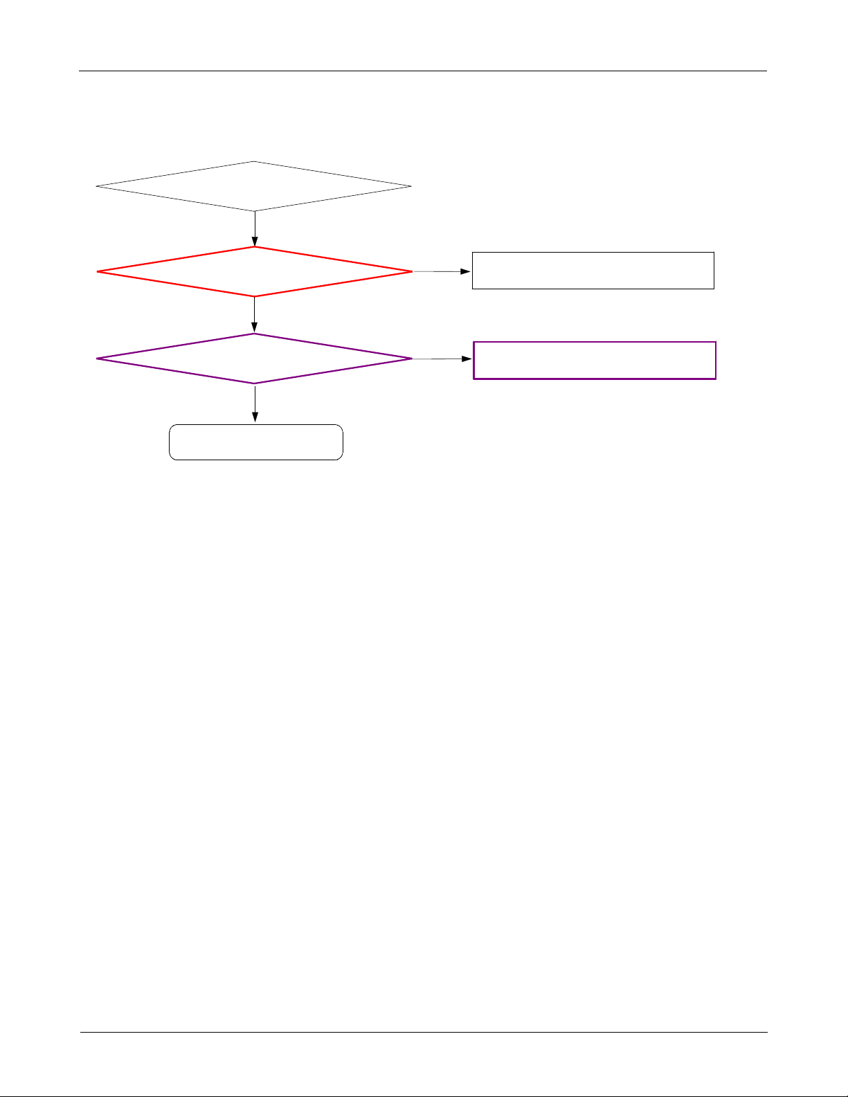
Flow Chart of Troubleshooting
8-3.
Equipments
Oscilloscope
Power Supply
Digital Multi-meter
driver, ESD Safe Tweezer
+
8960 &
Confidential and proprietary-the contents in this service guide subject to change without prior notice.
Distribution, transmission, or infringement of any content or data from this document without Samsung’swritten authorization is strictly prohibited.
Spectrum Analyzer
8-4
Soldering iron
Page 5

Level3Repair
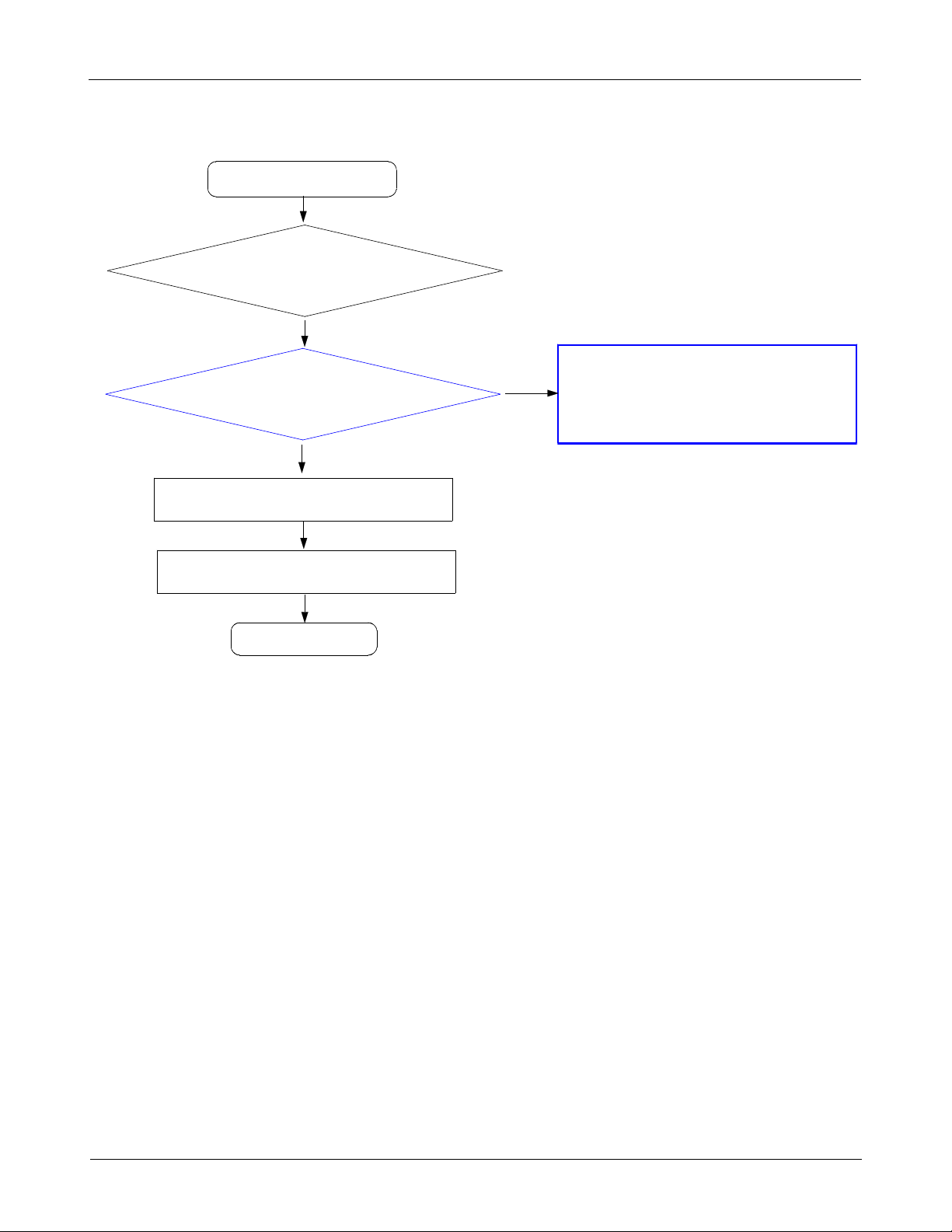
8-3-1.
Power On
Mobile phone does not power on.
Check the Battery Voltage
it more than
Is
Yes
Power-on the phone and
check the power-on sound
or motor Vibration.
No
Check the TACT500
soldering crack, open, etc)
(
3.8
V?
.
No
Yes
Abnormal
If its voltage level is extremely low(under
Change the TACT500(Power-key switch)
Charging the battery by TA.
Change the battery.
Change the FRONT-LCD ASSY
And retry to the power-on operation.
3.0
V),
Yes
Check the U403 output voltage
C416
(
Check the Clock OSC400
Is that frequency
check the initial operation
>1.8
V, C418
Yes
Yes
Yes
END
>1.2
32.768
V)
Khz?
No
No
If the output voltage is not satisfied with normal
condition, Change the U406.
Each voltage level has
※
Change the OSC400.
If OSC400 does not still work, Change the U406
This problem is internal oscillator of U406.
Test condition(Oscilloscope setting)
※
us.div(time division)
:20.0
±10%
margin.
8-5
Confidential and proprietary-the contents in this service guide subject to change without prior notice.
Distribution, transmission, or infringement of any content or data from this document without Samsung’swritten authorization is strictly prohibited.
Page 6
Level3Repair
F
BOTHHOLE101
TP_NFC_CLK_REQ
TP_FM_I202
TP_FM_I200
TP_FM_I203
P
T
U
O
_
B
R
C
C
R
R
I
V
_
5
4
4
5
5
P
T
2
2
6
1
2
0
5
9
1
N
T
U
O
_
B
I
V
_
P
T
5
2
4
C
C476
C
4
6
2
3
1
7
4
C
C426
C
C
4
4
5
4
3
4
9
4
4
C
C
4
7
0
C
4
4
0
C
4
6
3
C469
9
8
3
3
4
4
C
R
7
C
6
4
L
4
1
3
C
7
4
2
8
6
4
C
C473
C486
C474
0
0
C
L
4
4
4
0
1
9
7
C
S
O
6
3
4
C493
C
C
4
C
7
2
4
6
1
C
6
6
4
C455
C
4
4
0
0
4
3
4
0
4
L
L
3
0
4
C
U
4
0
6
L
L
4
4
1
0
0
8
4
C
1
8
R
4
2
8
1
1
0
3
4
4
R
R
C
4
3
5
C562
3
6
5
C
C
5
5
8
4
4
5
C
C
5
6
4
5
8
4
C
C550
C
4
2
0
R
5
4
7
R
4
1
3
R542
C549
9
5
C
C
4
4
4
6
9
C
0
1
8
4
C
4
8
4
5
C
C
C
C
4
4
4
2
2
2
9
2
9
8
8
4
C
C
4
4
9
C
4
2
L412
0
C
4
8
3
L401
1
C400
L402
C
5
4
2
7
7
5
4
C
1
6
1
4
C
8
6
5
5
4
4
C
C
L
4
0
L
6
4
0
7
4
1
4
C
0
0
4
H
2
7
T
9
5
4
4
C
C
C
4
2
3
4
4
3
4
1
C
4
L
TP_BT_UART_CTD
TP_BT_UART_RXD
2
0
1
T
P
_
I
F
_
R
X
D
T
P
_
I
F
_
T
X
D
C
C
3
3
1
1
1
4
6
1
3
C
C
C
3
3
1
1
9
8
C
3
4
C
0
0
1
C375
C302
C450
C
4
C451
C
4
4
3
T
P
_
P
O
R
N
9
T
8
P
_
R
4
E
S
E
T
C
C421
TP_BT_VREG_ON
C
4
4
3
5
0
R
TP_BT_UART_TXD
R
R
3
3
1
1
6
7
C
3
1
5
2
3
1
1
3
3
C
C
TP_BT_UART_RTS
0
R
0
5
C
0
5
2
C
4
3
5
7
4
3
C
C
3
7
7
1
4
3
C
C
5
3
6
C
8
4
3
5
C
7
4
C464
R
1
3
9
3
0
0
R
9
2
3
C
T
P
_
3
0
1
5
Q
C324
C
3
3
2
C325
C
C
3
3
2
0
6
6
C348
5
8
0
2
0
0
6
3
3
3
3
3
C
C
C
C
VSMPSA_LX
VSMPSA_VIN
VSMPSB_VIN
VSMPSB_LX
VSAFE_VIN
VSAFE_LX
C414
VSMPS1_1V2
L406
VBAT
C415
L408
10V
L407
C416
1005
VSMPS2_1V8
VSMPS2_1V8_VIN
VSMPS2_1V8_R
VBAT
L409
C417
L410
C486 OPEN
C493
1005
OSC400
1005
CP_VSIM
3
0
5
6
0
0
0
1
0
2
0
9
4
4
H
C
T
1107
1005
C418
MSP1_TCK
FM_I2S_CLK
WGBF_32K_CLOCK
MSP1_TXD
AP_DM
AP_DP
I2C_APE_SCL
I2C_APE_SDA
SIM_CLK
SIM_DAT
SIM_RST
CLK32KOUT1
RCV_N
RCV_P
BAT_CTRL
C485
1005
VSMPS3_1V2
APESCL
J17
APESDA
R9
BATCTRL
P9
BATTEMP
P4
BITCLK1
P3
BITCLK2
K2
CFHSN
K1
CFHSP
M14
CISOCLOCK
N14
CISODATA
P13
CISORESET
C15
CLK32KOUT1
C17
CLK32KOUT2
U16
XTALINCLK32K
T17
XTALOUTCLK32K
P14
CUSBDM
P15
CUSBDP
P1
DADATA1
N3
DADATA2
D1
DM
C1
DP
H1
EARN
H2
EARP
I2C
TEMP/VF
Chare Pump Ext Cap
SIM I/F
32KHz Block
SIM DP/DM
DA data
USB data
8-6
Confidential and proprietary-the contents in this service guide subject to change without prior notice.
Distribution, transmission, or infringement of any content or data from this document without Samsung’swritten authorization is strictly prohibited.
Page 7
Level3Repair
8-3-2.
Initial
Initial Failure
Yes
Re-download latest SW on the
Check the oscillator clock waveform.
mobile phone.
Abnormal
KHz:OSC400,
32.768
MHz:OSC200
37.4
Normal
Change UCP300,U406
Abnormal
Change PBA
Abnormal
Check the OSC400, OSC200.
Crack, open etc.)
(
Check the output clock waveforms and frequency.
Test condition(Oscilloscope setting)
※
us.div(time division)
:20.0
END
8-7
Confidential and proprietary-the contents in this service guide subject to change without prior notice.
Distribution, transmission, or infringement of any content or data from this document without Samsung’swritten authorization is strictly prohibited.
Page 8

Level3Repair
BOTHHOLE101
7
2
3
R
3
2
3
2
0
4
C
P
T
U
O
_
B
R
I
V
_
5
P
T
2
1
N
T
U
O
_
B
I
V
_
P
T
C
4
6
2
C482
C
C
R
R
4
4
5
5
2
6
1
2
3
5
9
0
5
1
2
7
4
4
C
C
C426
C
C
4
4
5
4
3
4
9
4
C469
9
4
8
3
3
4
C
4
C
R
C476
4
L
1
3
7
4
2
8
6
4
C
C473
C486
C474
C
4
7
0
0
0
L
4
4
0
9
C
C
4
4
S
0
O
C
4
6
6
3
3
4
C493
C
C
4
C
7
2
4
6
1
9
9
C
4
Y
D
R
D
_
5
2
2
C
S
S
A
P
M
O
C
_
P
T
9
0
2
4
2
2
C
U
R
R
3
3
6
2
2
5
8
9
5
C
C455
C
4
4
0
0
4
4
L
7
6
4
C
C
C
4
L
1
L
7
4
4
1
0
0
8
8
1
4
C
R
4
1
3
C
4
3
5
5
1
4
T
P
R
_
G
N
D
_
D
E
T
_
A
B
4
0
0
3
2
2
C
4
1
3
R
5
1
3
R
R
5
4
7
C
5
5
8
1
4
4
5
3
C
0
4
L
C
5
6
4
R542
5
8
C
4
3
0
4
C
C550
U
4
0
6
5
1
4
C
L
4
0
7
6
1
4
C
2
8
1
0
4
4
R
R
8
6
5
5
4
4
R
C
C
4
9
2
1
0
4
R
2
7
2
4
0
2
U
3
7
2
C
C274
9
5
C
4
4
6
C
0
1
8
4
C
3
4
R
C549
C
C
C
4
4
4
2
2
8
9
2
8
4
8
4
C
4
9
C
4
L412
8
L401
C400
L402
2
5
4
C
L
4
0
6
4
1
4
C
4
1
4
L
0
0
4
H
7
2
T
5
9
4
4
C
C
S
E
R
V
I
C
E
_
A
B
8
5
0
5
C
T
P
3
0
0
TP303
1
R340
R
3
1
C
T
7
P
4
_
9
I
F
_
5
T
X
D
C
C
C
3
3
C
4
2
0
1
0
7
7
4
9
8
4
C
C
4
3
3
C
3
6
3
2
6
3
4
C
C
U306
C
U308
5
0
3
P
T
3
1
1
1
1
4
5
3
2
1
1
3
3
C
C
6
0
0
5
R
1
3
C
2
0
5
C
C
C
C
3
3
4
1
1
5
8
9
4
C
3
7
0
1
1
3
C
6
5
3
C375
3
8
4
C302
5
7
4
C450
C464
C451
9
1
3
4
3
4
C
T
P
0
0
_
P
O
R
N
T
P
_
R
E
S
E
T
C421
TP_BT_VREG_ON
T
3
4
4
C
P
_
3
0
1
C370
5
3
3
R
2
5
3
C
C369
0
3
P
T
7
TP309
7
6
3
6
C
6
3
C
Q
E
R
_
K
L
C
_
S
Y
S
_
P
T
C
4
2
9
3
4
C
2
4
4
C
4
3
R
C368
C
R
3
1
6
C325
C
C
3
3
0
2
6
6
C348
TP_BT_UART_RTS
3
7
3
C
C
3
7
4
C
C
C
R
3
R
5
8
0
9
0
0
6
2
3
3
3
3
C
C
C
C
N
_
T
S
R
_
TP_WLAN_SDIO_DATA0
TP_WLAN_SDIO_DATA2
TP_WLAN_SDIO_CMD
N
A
L
W
_
P
T
C
C
C
C
C
3
3
3
3
3
4
4
5
6
0
3
2
7
5
7
U
C
P
3
0
0
5
2
3
4
3
4
2
3
3
C
E
K
A
W
_
T
B
_
P
T
R
4
1
6
3
1
3
C
C
R
U
M
E
3
0
1
TP_RF_STROBE
6
4
7
3
4
5
C
3
7
2
0
C
5
C
0
1
3
3
4
4
1
0
1
0
4
8
7
3
3
3
3
C
2
2
3
3
3
3
C
C
C
C
4
3
C
C
C
C
C
3
3
3
3
3
5
7
2
L
2
1
C
2
2
R
0
6
2
C
C
3
3
7
8
6
2
C
C255
U207
R232
3
7
3
0
2
3
4
2
2
R
R
R
R
2
1
0
2
0
3
R
C
4
3
9
C
5
3
1
1
3
0
R
0
3
9
R
3
3
3
C
2
7
3
C
R326
1
2
3
C
9
3
3
C
9
5
3
C
8
5
3
C
6
3
3
C
2
2
3
C
8
3
3
C
8
0
0
1
3
3
P
P
T
T
0
N
0
I
N
3
_
D
T
B
P
T
C361
R332
R331
R334
R305
R304
R333
R330
R308
R303
R306
4
5
3
C
9
1
L211
2
R
2
0
4
C240
1
6
2
C
C267
C269
6
4
2
C
C262
8
R
6
5
0
1
2
R
3
2
8
C
TP_HOST_WAKE
2
4
2
5
5
5
U
R
C245
O
S
C
2
0
1
L111
0
0
1
C
S
1
9
7
L
1
3
1
R
C243
F203
1
7
5
4
2
2
C
C
3
2
9
C
C
2
7
9
C210
U
C296
2
9
2
9
C
L209
C
0
8
R
2
0
7
R
3
4
2
R
2
6
7
3
3
3
2
2
6
C
C
C
C
2
2
8
4
2
4
R230
1
8
7
5
6
1
C
2
U101
C
1
7
5
C176
4
3
4
7
1
1
C
C
1
0
C
S
1
C
2
2
1
5
2
2
C
9
8
5
4
3
3
3
3
2
2
2
2
R
R
C
C
C
C
2
2
4
1
1
1
7
8
2
5
2
3
C
C
U201
C297
L206
C
C298
2
0
5
C
C
2
4
8
2
2
1
8
2
8
5
2
2
C
C
2
4
9
C
7
2
2
C
8
7
2
1
2
2
C
L
2
8
8
C
C
2
8
0
2
0
7
C
5
1
2
L
8
7
2
C
1
7
2
C
8
0
2
L
6
5
2
C
7
7
2
C
C275
2
5
C
0
8
C
5
2
2
C
5
1
2
L
0
7
TP_WLAN_SDIO_DATA1
TP_WLAN_SDIO_DATA3
2
0
1
C
S
C
L135
1
L
4
4
6
1
C
2
1
1
R
2
6
1
C
0
8
1
C
S
C
1
0
3
L
1
3
1
4
0
L
9
8-8
Confidential and proprietary-the contents in this service guide subject to change without prior notice.
Distribution, transmission, or infringement of any content or data from this document without Samsung’swritten authorization is strictly prohibited.
Page 9

Level3Repair
8-3-3.
No Service
No service
Yes
Check memu setting
Menu→applications→setting→wireless and network
mobile networks→network mode→setting is auto mode
Menu→Phone→Keypad
*#1234#
C108,L109,L143,C181,L127,F101 is
check Phone version
→
PHONE:I8190XXXX
No
Check the
well soldered
→
→
→
?
PHONE:I8190XXXX
No
Check the Main Antenna exists or not
Re-solder C108,L109,L143,C181,L127,F101
correspondingly.
Yes
Check VREF
VREF(C129)
Change the Main Antenna
Change the PBA
=2.5V
Abnormal
Abnormal
Yes
END
No
Replace the U101
8-9
Confidential and proprietary-the contents in this service guide subject to change without prior notice.
Distribution, transmission, or infringement of any content or data from this document without Samsung’swritten authorization is strictly prohibited.
Page 10
Level3Repair
R557
R
6
5
C109
L143
1
8
1
2
C
L
1
7
0
S
0
F
1
1
0
0
0
1
1
T
T
N
N
A
A
R
1
2
6
2
2
0
1
1
1
L
C
C
T
_
T
A
D
_
P
T
C
_
P
T
T
_
K
L
8
1
1
C
C
1
0
7
4
0
1
C
S
C
1
0
6
C
S
0
1
0
5
0
4
U
C542
6
1
L
4
ZD500
5
0
S
C
1
0
L
4
1
2
F106
4
4
5
9
0
0
1
C
U
1
0
0
O
2
0
1
2
0
1
1
1
1
1
L
2
0
L
C
C
1
3
1
0
3
1
C
C116
0
Q
0
1
6
0
1
C
1
C
C
R
7
3
1
C
F
1
7
0
8
2
1
L
9
3
1
C
3
4
1
C
7
4
L
1
1
L
3
3
8
4
1
C
8
0
1
1
4
1
C
6
4
L
1
F
1
L
3
0
2
4
1
C
C100
3
0
1
L
F100
C101
C
1
1
5
1
7
C
1
L
1
4
0
1
5
1
C
S
C
L
1
1
C134
1
2
L
6
3
1
1
0
C136
F102
C
1
7
2
1
8
1
L
5
L516
5
0
8
Z
D
1
1
5
D
C
2
5
7
HDC504
Z
HDC502
7
C
0
S
1
C
1
1
3
L
L
1
1
2
2
6
5
L121
5
0
1
F
2
L
4
1
L120
7
C160
C130
5
3
C
1
C182
9
1
1
L
1
0
1
L
0
0
1
L
L123
8
1
0
1
L
L
1
2
0
0
0
7
1
C
1
F
5
1
1
L
C
L
2
1
9
C
1
1
2
1
1
1
3
2
1
L
7
2
L
1
1
8
C157
C
1
F103
1
C146
8
0
4
5
C
1
C151
C
1
5
9
L
1
3
C172
4
0
A
1
M
0
0
1
F
L
1
8
0
0
9
1
C
4
L
1
2
3
5
5
1
1
C
C
1
C
S
BOTHHOLE108
0
C
1
5
9
6
1
C
7
6
1
C
C
1
6
6
P
6
5
1
C
S
C
1
0
9
1
6
1
8
3
C
1
L
8
5
1
C
RFS100
9
1
4
6
6
1
1
1
1
1
D
D
D
D
D
D
N
N
N
N
N
N
G
G
G
G
G
G
TXL
18
TXH
17
CTLC
9
CTLB
8
CTLA
7
TRX6
13
TRX5
12
TRX4
5
TRX3
F101
T
N
A
5
1
4
TRX2
3
TRX1
2
D
D
V
VHI_2V5
0
1
C129
V
6
1
C109
OPEN
ANT100
1
1
2
2
L143
1005
C181
G
G
C
A
4
3
2
1
C108
50V
1005
5
0
0
1
L109
ANT101
1
1
2
2
5
5
0
0
0
0
1
1
5
0
0
1
L127
8-10
Confidential and proprietary-the contents in this service guide subject to change without prior notice.
Distribution, transmission, or infringement of any content or data from this document without Samsung’swritten authorization is strictly prohibited.
Page 11

Level3Repair
8-3-4.
Sim Part
Insert SIM card
Yes
Is SIM/SD assy well
connected to main board?
Yes
Check the SIM Voltage.
C519)
(
>= 1.8or3.0?
Yes
END
No
No
Reassemble SIM/SD assy and still SIM
does not work, replace SIM/SD assy
Change to the new SIM card.
If it doesn`t still work SIM card after changeing
the SIM card, Check the UCP300(Crack etc)
HDC503
A
N
T
2
0
R
C
V
5
0
L
5
2
0
1
L
5
1
9
5
I
M
0
S
0
0
NFC_SIMVCC_3.0V CP_VSIM
R560
C208
C
2
0
3
C207
L204
1
0
2
F
L
2
0
2
U200
3
8
2
C
C204
2
0
L
0
C209
C
C
5
3
5
5
4
1
7
1
2
7
9
5
5
0
5
C
R
C
NFC_SWP SIM_RST
R515
C573
6
5
4
SIM500
6
5
4
7GG89GG10
11
33
22
C519
5
0
0
1
C574
SIM_CLKSIM_DAT
C520
8-11
Confidential and proprietary-the contents in this service guide subject to change without prior notice.
Distribution, transmission, or infringement of any content or data from this document without Samsung’swritten authorization is strictly prohibited.
Page 12
Level3Repair
8-3-5.
Charging Part
TA/USB Insert
Charging Sequence Start
Battery is Charging?
C510
END
Yes
=5V
Yes
Yes
No
No
Reconnect TA or USB
Resolder or Replace L400
8-12
Confidential and proprietary-the contents in this service guide subject to change without prior notice.
Distribution, transmission, or infringement of any content or data from this document without Samsung’swritten authorization is strictly prohibited.
Page 13

Level3Repair
8-3-6.
Microphone Part
Check microphone function
in voice call receiver mode
or in Voice Recording mode
Check the main MIC is
placed for any damage
Check the voltage at
C551
Yes
Yes
=2.1V
No
No
Resolder the main MIC
Resolder or replace C551
Yes
Check component soldering
statuses of
C549,C550,L510,L511
Yes
END
No
Resolder or replace C549,C550,L510,L511
8-13
Confidential and proprietary-the contents in this service guide subject to change without prior notice.
Distribution, transmission, or infringement of any content or data from this document without Samsung’swritten authorization is strictly prohibited.
Page 14

Level3Repair
VAMIC2_2V1
9
0
5
L
5
0
0
1
MIC500
OUT
OUT
4
GND2GND
3
GND1GND
2
POWER
POWER
1
C551
2
3
0
2
6
0
T
L
1
5
O
0
0
5
0
V
C
1
D
N
Z
L510
L511
1005
1005
R542
4
5
0
0
0
5
1
C
5
0
0
1
NC
C549 10V
C550
Near by AB8505
MIC2P
10V
MIC2N
2
F103
C
L
1
1
7
1
2
1
8
8
1
0
S
6
1
C
L
C146
S
8
1
C
0
3
5
5
1
1
C
C
BOTHHOLE103
BOTHHOLE110
C
C
5
5
ZD401
2
2
6
5
R
C504
9
0
5
L
C551
1
0
5
D
Z
MIC500
6
4
C
6
C455
C
C
4
4
2
6
3
5
C426
C
4
5
3
C469
9
3
4
C
7
4
C
6
C
4
4
0
0
4
4
L
3
6
5
C
C
5
5
8
4
4
5
3
C
0
4
L
C
5
6
4
5
8
3
0
4
C
4
C
C550
2
4
C
0
R
5
4
7
8
1
4
C
R
3
4
1
C
C
4
4
8
9
4
8
R542
C549
U
4
1
3
L
4
C
2
7
4
0
6
5
5
9
0
U
2
5
508
F
0
1
1
1
5
5
L
L
R
5
5
8
9
5
4
C
2
2
4
C
4
2
3
3
5
5
R
R
R536
IFC500
C
4
2
8
C
C
5
5
4
4
0
1
BOTHHOLE106
C
5
0
3
9
4
4
C
BOTHHOLE104
L412
L401
C400
L402
C473
C486
C474
0
C
0
L
4
4
4
C
S
O
L
0
1
9
7
4
1
0
5
1
4
L
4
0
8
C
4
C
2
5
L
4
0
6
8-14
Confidential and proprietary-the contents in this service guide subject to change without prior notice.
Distribution, transmission, or infringement of any content or data from this document without Samsung’swritten authorization is strictly prohibited.
Page 15

Level3Repair
8-3-7.
Speaker Part
Play MP3 with maximum volume level.
Check speaker function.
Yes
Check the connection of
Speaker module
Yes
Check the signals on
L522, L521
No
No
Reconnect speaker or replace speaker
module
Resolder or replace L522, L521
END
Yes
8-15
Confidential and proprietary-the contents in this service guide subject to change without prior notice.
Distribution, transmission, or infringement of any content or data from this document without Samsung’swritten authorization is strictly prohibited.
Page 16

Level3Repair
R
L
OTHHOLE102
U205
L
5
2
1
2
Z
D
5
0
T
P
_
V
T
_
R
E
S
E
T
C
5
0
0
S
L
3
C
7
5
7
7
4
5
C
L
5
ZD510
1
5
D
0
Z
8
7
L
1
5
8
5
2
4
2
L
5
C
FM_ANT
EAR_COM
C577
L522
1005
SPK_P
L521
1005
2
3
0
7
8
5
4
4
0
5
5
0
C
1
C
0
5
5
D
D
Z
Z
T
T
L
L
O
O
V
V
SPK_N
HDC503
11
334
556
T
L
O
V
ZD510
778
99
NC
11
12 13
L518
1005
1005
L517
L512
2
2
L513
4
6
L514
8
L515
10
10
NC
NCNC
14
R510
0603
T
L
O
V
6
5
4
3
1
ZD507
2
3PI_DETECT
EAR_MIC_CON
3PI_ADC
R544
R549
5
5
0
0
0
0
1
1
C560
C559
C569
R553
1005
C570
1005
EAR_SPK_
EAR_SPK_
8-16
Confidential and proprietary-the contents in this service guide subject to change without prior notice.
Distribution, transmission, or infringement of any content or data from this document without Samsung’swritten authorization is strictly prohibited.
Page 17

Level3Repair
8-3-8
Receiver Part
Check receiver function
in voice call receiver mode.
Yes
Check the receiver module
for any damage(tear in
FPCB, crack, etc)
No
Check the signals on C578,
C579, L519, L520
Yes
Yes
No
Replace receiver module
Replace and resolder C578, C579, L519,
L520
Replace TSP, LCD front
Ass'y
END
8-17
Confidential and proprietary-the contents in this service guide subject to change without prior notice.
Distribution, transmission, or infringement of any content or data from this document without Samsung’swritten authorization is strictly prohibited.
Page 18

Level3Repair
RCV_P
RCV_N
HDC503
RCV501
L519
L520
0603
0603
4
5
0
0
5
5
D
D
Z
Z
T
L
C578
5
0
0
1
C579
5
0
0
1
O
V
R
1
1
2
2
A
N
T
2
0
0
C
V
5
0
1
L
5
2
0
L
5
1
9
Z
D
5
0
T
P
_
V
T
_
R
E
S
E
T
0
0
T
P
_
V
T
_
S
T
B
Y
F501F503
C
C290
2
2
6
R
2
0
8
C569
R
5
5
3
C559
5
4
9
R
5
4
4
C
5
7
0
S
L
C
5
G
B
I
T
N
_
T
P
R
5
1
2
L
5
1
0
C517
L
5
0
2
C518
ZD507
L515
R
L
5
1
3
C561
L514
C56
0
R20
4
ZD505
C211
4
D
5
Z
0
8
7
5
C
C579
R203
6
1
5
C
P
_
P
T
C
C
C231
4
4
0
3
7
C
4
1
0
C
4
0
5
0
1
0
4
U
C409
7
1
4
R
C
4
0
8
C
4
1
1
0
0
4
L
C
4
0
6
R
3
R
3
1
1
1
2
3
7
L
1
5
8
5
2
4
2
L
5
C
8-18
Confidential and proprietary-the contents in this service guide subject to change without prior notice.
Distribution, transmission, or infringement of any content or data from this document without Samsung’swritten authorization is strictly prohibited.
Page 19

Level3Repair
8-3-9.
BT/WIFI
BT/WiFi is not working
Yes
Check BT or WiFi function
Check
Check the Status of
C216, C214, ANT201
ON
Yes
MHz Clock at
37.4
R205
Yes
Yes
No
No
No
Enable BT or WiFi Function
Check the OSC201(crack, open, etc.)
Resolder or Replace C216, C214, ANT201
Replace BT/WIFI Antenna
Yes
END
8-19
Confidential and proprietary-the contents in this service guide subject to change without prior notice.
Distribution, transmission, or infringement of any content or data from this document without Samsung’swritten authorization is strictly prohibited.
Page 20

Level3Repair
N
WLAN_TX
WLAN_RX
BT_RF
C217
6
4
5
3
D
D
T
N
N
R
G
G
O
P
U201
D
N
G
0
1
VCTL3
3
ANT
2
VCTL1
1
1
2
T
L
R
T
O
C
C
C
P
V
N
N
4
3
1
2
1
1
1
1
C214
SW_WLAN_TX
SW_WLAN_RX
SW_BT
GND
7
PORT2
8
GND
9
F202
1
2
IN OUT
GND
L205
3
C216
L207
ANT201
1
1
2
2
C281
XTAL_OUT
R205
C226
C221
C220
OSC201
2
C222
43
1
XTAL_I
C227
8-20
Confidential and proprietary-the contents in this service guide subject to change without prior notice.
Distribution, transmission, or infringement of any content or data from this document without Samsung’swritten authorization is strictly prohibited.
Page 21

Level3Repair
8-3-10.
FM RADIO
FM Radio is not working
Check the Connection of E/P
Check the HDC501 connector
Jack FPCB
Check the Status of C574,
L513, L509
Yes
Yes
Yes
Yes
No
No
No
Reassemble or replace E/P Jack FPCB
Repalce the board
Resolder or Replace C574, L513, L509
Resolder or Replace U206
Yes
END
8-21
Confidential and proprietary-the contents in this service guide subject to change without prior notice.
Distribution, transmission, or infringement of any content or data from this document without Samsung’swritten authorization is strictly prohibited.
Page 22

Level3Repair
FM_ANT
C574
L513
ZD502
L509
11
33
55
77
99
NC
11 12
HDC501
NC
NC
13 14
L505
2
2
4
L506
4
6
6
L507
8
8
L508
10
10
NC
EAR_COM
R541
OPEN
R543
T
R
O
H
S
8-22
Confidential and proprietary-the contents in this service guide subject to change without prior notice.
Distribution, transmission, or infringement of any content or data from this document without Samsung’swritten authorization is strictly prohibited.
Page 23

Level3Repair
8-3-11.
LCD
LCD is still off after PWR ON
Yes
Check the connection of
Check the soldering status of
Check C479=3.0V, C480=1.8V
HDC500
Yes
EMI Filters
Yes
No
No
No
Reassemble FRONT assy
Resoldering EMI Filters
F505,F506,F507)
(
Resolder or Replace the U402,U403
Yes
Replace LCD
Module
Yes
END
8-23
Confidential and proprietary-the contents in this service guide subject to change without prior notice.
Distribution, transmission, or infringement of any content or data from this document without Samsung’swritten authorization is strictly prohibited.
Page 24

Level3Repair
F
F
LCD_RST
LCD_VGH_5.2V
EL_ON
LCD_D0_N_F
LCD_D0_P_F
LCD_CLK_N_F
LCD_CLK_P_F
LCD_D1_N_F
LCD_D1_P_F
VREG_LCD_3.0V
R561
0603
VREG_LCD_1.8V
C534
5
0
0
1
44
10 10
20
22
24
26
28
30
32
34
HDC500
22
14
16
18
20
22
24
26
28
30
32
34
38
NCNC
NC
37
ELVDD_4.6V
11
33
5566
7788
99
11 1112 12
13
1314
15
1516
17
1718
19
19
21
21
23
23
25
25
27
1005
27
29
1005
29
31
31
33
33
NC
3536
ELVSS_-4.9V
L507
L508
MTPHV
MTPHV
F505
4
I|O
3
VREG_TSP_1V8
LCD_D0_N LCD_D0_N_F
LCD_D0_P LCD_D0_P_F
VREG_TSP_A3V3
FLMLDI_ESD_DET
R519
R521
R520
5
5
5
0
0
0
0
0
0
1
1
1
ELVDD_FB
TSP_INT_1V8
TSP_SCL_1V8
TSP_SDA_1V8
C536
C535
5
5
0
0
0
0
1
1
LCD_CLK_N
LCD_CLK_P
LCD_D1_N
LCD_D1_P LCD_D1_P_F
4
I|O
I|O
4
I|O
I|O
1
I|O
2
I|OI|O
D
D
N
N
G
G
6
5
F506
1
I|O
I|O
D
D
N
N
G
G
5
6
LCD_CLK_N_
23
LCD_CLK_P_
F507
1
I|O
I|O
D
D
N
N
G
G
5
6
LCD_D1_N_F
23
T
A
C
T
5
0
1
C566
C568
T
A
C
T
5
0
2
LCD_PWR_EN
9
4
R
4
5
C569
0
C
7
5
3
R
5
5
C
2
0
1
P
T
U
O
_
B
R
R
R
I
C
V
_
5
5
5
4
P
T
1
2
2
6
9
0
1
5
N
T
U
O
_
B
I
V
_
P
T
5
1
2
7
4
4
C
C
R
4
5
C
2
3
0
9
2
2
C
2
1
2
C
L515
1
4
2
F200
R
OSC200
U
2
0
2
TP_NFC_CLK_REQ
TP_FM_I202
TP_FM_I200
TP_FM_I203
C
4
2
3
VBAT
U402
.
4
VIN VOUT
5
32
0
0
5
1
0
0
1
C478
GND
EN
D
N
G
5
R429
VREG_LCD_3.0V VREG_LCD_1.8V
1
LCD_PWR_EN
5
0
0
1
VBAT
U403
4
VIN VOUT
32
EN
1
GND
D
N
G
5
C479
5
0
0
1
C480
.
0
0
1
4
C
4
0
5
C409
5
9
2
C
3
2
2
C
R206
4
0
4
L
L
2
6
0
5
0
0
2
0
3
2
2
2
L
C
C
1
0
2
L
5
C
1
2
U
R205
2
T
P
6
0
2
0
0
2
7
P
T
3
T
P
2
0
200
5
T
P
2
0
TP200
4
2
0
C
2
C219
L207
6
6
C
4
C455
C
4
0
4
C562
3
6
5
2
0
4
C
R
5
4
7
1
8
4
C
5
5
8
1
R
3
4
4
C
4
4
5
3
0
4
L
8
C
4
C
5
6
4
L
0
4
U
0
6
C
4
R
3
7
1
R
1
3
1
1
2
4
R
BOTHHOLE107
C
C
4
T
P
_
5
M
_
S
T
B
Y
0
1
0
0
4
4
T
T
O
O
M
M
0
0
C510
0
0
5
0
0
5
U
7
1
8
0
0
1
5
5
5
R
R
C
C
9
5
C
4
4
6
C
0
C
C
C
C
4
4
4
2
2
9
2
2
8
8
9
4
C
4
L
3
0
5
L
C527
4
C530
6
9
0
0
5
5
R
R
C531
R526
TP_BT_UART_CTD TP_BT_UART_RXD
T
P
_
I
F
_
R
X
D
R
3
1
C
T
7
P
4
_
9
I
F
_
5
T
X
D
C
C
C
3
3
3
1
1
1
5
4
1
0
1
S
5
L
C
2
1
C
5
3
1
C
T
P
_
5
M
_
R
E
S
E
D
C
4
8
8
3
3
5
C
0
5
L
TP_BT_UART_TXD
C324
R
3
1
6
C325
C348
T
F500F502 F504
C532
5
0
U
5
0
3
2
1
5
R
5
L
8
2
5
C
TP_BT_PCM_CLK OD_MCP_TB_PTID_MCP_TB_PTTP_BT_PCM_SYNC
T
P
2
2
8
6
R
1
5
0
0
5
R517
Q
7
R
2
3
3
C
2
3
C
C
C
C
C
3
3
3
3
3
5
0
2
0
6
7
6
6
7
5
5
R561
1
0
5
L
C534
5
1
5
C
F
5
0
4
1
5
5
C
F
5
0
6
6
0
5
L
C535
L507
C536
L508
9
F
2
5
5
0
C
7
T
P
2
R
4
3
2
2
9
3
0
4
0
8
4
C478
C
U
9
2
4
R
2
0
9
7
C
4
4
U
C
C
C
C
C
C
3
4
3
3
3
3
3
3
3
2
7
4
5
5
0
1
2
0
9
1
0
U404
5
4
R
7
8
4
C
H
D
C
5
0
0
1
0
2
C
2
4
5
6
2
5
C
Q
6
4
7
3
4
5
C
3
7
4
C
2
3
2
C
R
0
C
6
2
C
C
C
3
3
3
4
4
3
1
0
7
8
C
6
2
7
R436
6
7
2
C
C249
C
2
1
3
6
4
6
6
6
2
4
2
2
C
C
C
2
1
2
L
L211
5
6
9
4
C
6
5
L
4
1
5
ZD400
C
9
4
7
6
8
8
2
2
C
C
2
9
5
4
2
2
C
9
1
2
R
C240
1
C
6
2
C
2
0
2
F
0
4
2
R
4
8
9
3
3
3
2
2
2
C243
C
R
R
TACT500
BOTHHOLE10 9
L
2
4
1
1
6
2
L
C
2
2
1
2
5
2
C
5
3
2
C
C
C
4
2
2
1
1
1
7
8
2
3
5
2
C
C
U207
8-24
Confidential and proprietary-the contents in this service guide subject to change without prior notice.
Distribution, transmission, or infringement of any content or data from this document without Samsung’swritten authorization is strictly prohibited.
Page 25

Level3Repair
8-3-12.
TSP
Touch Screen does not work
Yes
Check the connection of
HDC500
Yes
Check C535=3.3V,
C536=1.8V
Yes
Replace LCD Module
No
No
Reconnect the Connecter of HDC500
Resolder C535, C536
END
Yes
8-25
Confidential and proprietary-the contents in this service guide subject to change without prior notice.
Distribution, transmission, or infringement of any content or data from this document without Samsung’swritten authorization is strictly prohibited.
Page 26

Level3Repair
LCD_RST
LCD_VGH_5.2V
EL_ON
LCD_D0_N_F
LCD_D0_P_F
LCD_CLK_N_F
LCD_CLK_P_F
LCD_D1_N_F
LCD_D1_P_F
C569
3
R
5
5
4
R
4
5
0
C
7
5
VREG_LCD_3.0V
R561
0603
L515
9
R
4
5
VREG_LCD_1.8V
C534
5
0
0
1
C
4
0
5
C409
44
10 10
20
22
24
26
28
30
32
34
1
0
4
U
7
1
4
R
HDC500
22
14
16
18
20
22
24
26
28
30
32
34
38
R
3
1
2
NCNC
NC
37
0
0
4
L
C
4
0
6
1
R
1
3
ELVDD_4.6V
11
33
5566
7788
99
11 1112 12
13
1314
15
1516
17
1718
19
19
21
21
23
23
25
25
27
1005
27
29
1005
29
31
31
33
33
NC
3536
ELVSS_-4.9V
L507
L508
MTPHV
MTPHV
VREG_TSP_1V8
VREG_TSP_A3V3
FLMLDI_ESD_DET
R519
R520
R521
5
5
0
0
1
5
0
0
0
0
1
1
ELVDD_FB
TSP_INT_1V8
TSP_SCL_1V8
TSP_SDA_1V8
C536
C535
5
5
0
0
0
0
1
1
BOTHHOLE107
C
T
A
C
T
5
0
1
C566
C568
T
A
C
T
5
0
2
C
2
0
1
C
2
3
0
P
T
U
O
_
B
I
R
R
R
C
V
_
5
5
5
4
P
T
2
1
2
6
0
9
1
5
N
T
U
O
_
B
I
V
_
P
T
5
1
2
7
4
4
C
C
9
2
2
C
2
1
2
C
TP_NFC_CLK_REQ
TP_FM_I203
C
4
2
3
1
4
2
F200
R
OSC200
U
2
0
2
TP_FM_I202
TP_FM_I200
5
9
2
C
1
0
3
2
2
C
R206
4
0
4
L
L
2
6
0
5
0
0
2
0
3
2
2
2
L
C
C
2
L
C455
5
C
1
2
U
R205
2
T
P
6
0
0
2
2
0
7
P
T
3
T
P
2
0
200
5
T
P
2
0
TP200
4
2
C
0
2
C219
L207
6
4
6
C
3
6
5
C
C
5
5
C
8
4
4
0
4
4
5
3
C
0
4
L
C
5
6
4
8
0
5
R
C562
C
0
4
2
R
5
4
7
C
8
4
1
1
R
3
4
C
C
4
4
8
9
4
8
1
0
0
0
4
4
T
T
O
O
M
M
0
4
D
0
C510
L
0
5
0
0
0
5
U
6
9
7
1
0
0
0
1
5
5
5
5
R
R
R
C
T
P
_
I
F
_
R
X
D
9
5
C
C
4
4
4
6
9
C
0
5
C
3
C
C
1
4
4
2
4
2
2
2
8
9
4
C
C
4
8
8
3
0
5
L
C527
4
0
5
L
C530
C531
R526
TP_BT_UART_CTD TP_BT_UART_RXD
TP_BT_UART_TXD
C324
R
R
3
3
1
1
T
6
7
P
_
I
F
C325
_
T
X
D
C348
C
C
3
3
1
1
5
1
T
P
_
5
M
_
S
T
B
Y
L
C
5
0
1
S
2
C
1
5
C
1
5
T
P
_
5
M
_
R
E
S
E
T
F500F502 F504
3
3
5
C
C532
5
0
U
5
0
3
TP_BT_PCM_CLK OD_MCP_TB_PTID_MCP_TB_PTTP_BT_PCM_SYNC
2
1
5
R
5
L
8
2
5
C
T
P
2
2
8
6
R
1
5
0
0
5
R517
Q
R
2
3
7
C
2
3
3
C
C
C
C
C
3
3
3
3
3
5
0
0
2
6
7
7
6
6
5
3
R561
1
0
5
L
C534
5
1
5
C
F
5
0
4
1
5
5
C
F
5
0
6
6
0
5
L
L507
C535
L508
C536
9
F
2
5
5
0
C
7
T
P
2
R
3
2
4
2
9
3
0
4
0
C
8
C478
4
U
9
R
2
4
2
0
C
4
9
7
6
4
4
3
C
U
C
C
C
C
C
C
3
4
3
3
3
3
3
3
3
2
7
4
5
5
0
1
2
0
C
4
9
1
U404
7
8
4
C
H
D
C
5
0
0
1
0
2
C
2
4
6
5
5
2
C
Q
7
4
5
3
7
4
2
C
2
3
2
C
R
0
C
6
2
C
C
C
3
3
3
4
4
3
1
0
7
C
6
2
8
L
4
1
5
0
5
4
R
7
R436
6
7
2
C
C249
C
2
1
3
6
6
4
6
6
4
2
2
2
C
C
C
2
1
L
L211
U207
5
9
6
4
C
6
5
ZD400
C
9
4
7
6
8
8
2
2
C
C
2
9
4
5
2
2
C
9
1
2
R
C240
1
6
2
C
C
F
2
2
0
0
4
2
R
4
8
9
3
3
3
2
2
2
C243
C
R
R
TACT500
BOTHHOLE10 9
L
2
4
1
1
6
2
L
C
2
2
1
2
5
2
C
5
3
2
C
C
C
2
2
4
1
1
1
7
8
2
3
5
2
C
C
8-26
Confidential and proprietary-the contents in this service guide subject to change without prior notice.
Distribution, transmission, or infringement of any content or data from this document without Samsung’swritten authorization is strictly prohibited.
Page 27

Level3Repair
8-3-13. 5M
CAM
Camera" function does not work
"
Check the Camera
connector on Main PBA
Check the voltage
C512
=2.8V
C515
=1.2V
C513
=1.8V
C514
=2.8V
Check the F500, F502,
F504 for any damage(crack,
open, etc)
Yes
Abnormal
Yes
No
No
No
Reconnect the5MCam module on
SLC501
Replace U401
Replace F500, F502, F504
Yes
Replace the camera module
Yes
END
No
Change main board
8-27
Confidential and proprietary-the contents in this service guide subject to change without prior notice.
Distribution, transmission, or infringement of any content or data from this document without Samsung’swritten authorization is strictly prohibited.
Page 28

Level3Repair
8-3-14. 1.3M
CAM
Front Camera" function does not work
"
Yes
Check the Camera
connector on Main PBA
Abnormal
Check the voltage
C516
=1.8V
C517
=1.8V
C518
=2.8V
Yes
No
No
Reconnect the SLC500
Resolder or replace U500
Check F501, F503 for for
any damage(crack, open,
Yes
Replace front camera module
Yes
END
No
Resolder F501, F503
8-28
Confidential and proprietary-the contents in this service guide subject to change without prior notice.
Distribution, transmission, or infringement of any content or data from this document without Samsung’swritten authorization is strictly prohibited.
Page 29

Level3Repair
F500
MIPI_TX_DP_0 MIPI_TX_DP_0_F
MIPI_TX_DN_0
4
I|O
I|O
5
1
I|O
23
I|O
D
D
N
N
G
G
6
MIPI_TX_DN_0_F
F502
MIPI_TX_DN_1
MIPI_TX_DP_1 MIPI_TX_DP_1_F
4
I|O
3
5
1
I|O
I|OI|O
D
D
N
N
G
G
6
MIPI_TX_DN_1_F
2
F504
MIPI_TX_CP
MIPI_TX_CN
4
I|O
I|O
5
1
I|O
I|O
D
D
N
N
G
G
6
MIPI_TX_CP_F
23
MIPI_TX_CN_F
U205
VCAM_DP
VCAM_DN
VCAM_CKP
VCAM_CKN
F501
4
I|O
3
I|O
5
1
I|O
I|O
D
D
N
N
G
G
6
VCAM_DP_F
2
VCAM_DN_F
F503
4
I|O
I|O
5
1
I|O
I|O
D
D
N
N
G
G
6
VCAM_CKP_F
23
VCAM_CKN_F
BOTHHOLE102
T
A
C
T
5
0
1
C566
C568
T
A
C
T
5
0
2
F503
C569
L
5
7
5
7
C
7
2
4
1
5
C
L
5
1
ZD510
0
D
5
2
Z
8
Z
7
D
L
1
5
5
8
5
0
2
4
3
2
L
5
C527
C
1
A
0
D
P
R
3
2
4
BOTHHOLE107
T
P
_
5
M
_
S
T
B
Y
0
1
S
L
5
C
1
5
2
C
1
5
3
T
P
_
5
M
_
R
E
S
E
0
0
D
4
C
4
8
8
3
0
5
L
0
5
4
L
C531
T
F500
F502
3
3
5
C
TP_BT_PCM_SYNC
F504
C532
5
0
U
5
0
3
5
L
8
2
5
C
TP_BT_PCM_CLK OD_MCP_TB_PTID_MCP_TB_PT
C
R561
L
0
5
1
C534
5
1
5
C
F
5
0
4
1
5
5
C
F
5
0
6
6
0
5
L
L507
C535
L508
C536
9
F
2
5
5
0
C
7
3
TACT500
C
C
4
9
1
0
U404
5
4
R
7
8
4
C
R436
H
D
C
5
0
0
5
496
C
6
5
L
4
1
5
ZD400
7
9
4
C
T
P
_
V
T
_
R
E
S
E
T
0
5
0
L
S
C
T
P
_
V
T
_
S
T
B
Y
R
1
5
2
L
5
L
1
5
3
1
0
C517
0
5
2
L
F501
C518
ZD507
C
C290
2
2
6
C559
2
8
0
R
3
5
5
R
L515
4
5
9
R
4
5
4
R
7
5
0
C
C
1
2
0
4
1
2
F200
R
C
2
3
0
OSC200
9
2
2
C
U
2
2
3
2
C
0
2
2
1
2
C
R206
4
0
2
R
R203
C561
6
ZD505
L514
1
5
C
5
0
6
C
C579
5
L
9
2
2
0
6
5
C
0
0
2
0
3
2
2
2
L
C
C
1
0
2
L
U
R205
2
0
3
200
T
P
2
0
4
2
2
0
C
C219
L207
G
B
I
T
N
_
P
T
P
_
P
T
8
C
4
0
C
C
C
C211
C231
4
4
4
1
3
0
1
0
7
5
0
D
4
Z
C
4
1
0
C
5
8
7
C
4
0
5
C409
1
2
5
C
T
P
6
0
2
2
0
7
P
T
T
P
2
0
5
TP200
0
0
1
4
L
0
4
U
C
4
6
0
R
7
3
1
3
1
R
1
1
4
2
R
0
1
0
0
4
4
T
T
O
O
M
M
C510
L
0
5
0
0
0
5
U
C530
7
6
9
1
8
0
0
0
0
1
5
5
5
5
5
R
R
R
R
R526
C
8-29
Confidential and proprietary-the contents in this service guide subject to change without prior notice.
Distribution, transmission, or infringement of any content or data from this document without Samsung’swritten authorization is strictly prohibited.
Page 30

Level3Repair
8-3-15.
GSM
RX
850
NORMAL CONDITION
catch the channel?
No
Trouble occurs only in
GSM1800 band?
Yes
Check C137, C139, L128
soldering condition for
any damage(crack, open,
damage(crack, open,
etc)
No
Check F101 for any
etc)
No
NO
Yes
Yes
Try
CHECK soldered components
Repair procedure
8-3-3
C137, C139, L128
esolder or change
R
F101
Check U100 for any
damage(crack, open,
etc)
No
Change the board
END
Yes
esolder or change
R
U100
8-30
Confidential and proprietary-the contents in this service guide subject to change without prior notice.
Distribution, transmission, or infringement of any content or data from this document without Samsung’swritten authorization is strictly prohibited.
Page 31

Level3Repair
7
0
1
C
5
0
1
C
S
1
3
1
0
4
1
L
6
2
0
1
1
L
C
_
T
T
P
T
_
A
D
T
K
_
P
T
_
L
C
8
1
1
C
C
1
0
7
4
0
1
C
S
C
1
0
6
1
0
0
C
2
2
0
0
1
1
1
1
C
C
C
C
U
1
0
0
C
5
1
3
1
0
3
1
C
O
S
7
C116
4
1
1
C
1
Q
0
0
0
1
6
C
S
0
2
1
5
4
2
9
4
2
1
0
1
1
1
L
2
1
L
C
R
1
C
1
C
1
1
L
1
0
5
0
3
7
1
C
8
2
1
L
3
9
1
C
4
3
1
C
L
1
3
3
4
8
1
C
4
1
1
C
L
1
3
0
4
2
1
C
C100
3
0
1
L
C101
C134
L
1
1
0
C136
F106
7
1
0
8
0
1
F
F100
F102
L
1
2
5
L121
F
4
2
1
L
7
4
1
L
3
5
C
1
6
L123
4
1
L
8
0
1
L
L
1
2
0
0
7
1
C
C
L
1
1
5
1
2
1
6
3
1
L
2
1
1
L
7
C
1
2
C
L
1
1
7
1
2
1
8
8
1
L
L
1
2
6
L120
C130
9
C
L
1
1
1
1
3
2
F103
C
5
0
1
F
7
C160
C182
1
1
L
1
0
1
L
0
0
L
1
1
0
1
F
9
1
2
C
C157
C146
0
8
S
BOTHHOLE10 8
4
5
1
C
5
0
C
C151
C
1
5
9
1
3
L
C172
4
0
1
F
L
1
8
0
0
9
1
C
4
1
1
L
1
C
S
0
0
2
5
1
C
1
9
6
1
C
7
6
1
C
C
1
6
6
A
1
M
P
6
5
1
C
S
C
1
0
9
1
6
1
8
3
C
1
L
8
5
1
3
5
1
C
C
INP_B1
1
4
9
6
1
1
1
6
1
1
D
D
D
D
D
D
N
N
N
N
N
N
G
G
G
G
G
G
TRX6
TXL
18
17
9
8
7
13
TXH
TRX5
12
TRX4
5
CTLC
TRX3
4
F101
CTLB
TRX2
3
CTLA
TRX1
2
D
T
D
N
V
A
VHI_2V5
0
5
1
1
C129
V
6
1
B1_TRX
C123
0603
3
0
6
25V
0
L115
L116
INM_B1
3
0
6
0
50V
1005
5
0
0
1
L110
C136
50V
1005
1
8
RX RX
G
9
G
7
G
ANT
5
6
G
4
G
2
F102
TX
3
C128
3
0
6
0
7
1
1
L
10
RF1
12
RF2
6
0603
RF3
3
0
6
0
8
1
1
L
RF_OUT_HB
VHI_2V5
8
T
N
A
1
VDD
F103
2
V2
3
C127
V
V1
6
D
D
D
D
D
N
G
5
1
N
N
N
N
C
G
G
G
G
N
1
3
4
9
7
1
1
VBAT
RF_OUT_LB
2
T
N
GSM850_TX
RFC7
1
1
0
0
1
GSM900 / B8_TRX
G850_RX
PCS_RX
L141
5
0
0
1
L137
RF_OUT_HB
1005
5
0
0
1
V
C146
0
5
RF_OUT_LB
1005
DCS_RX
C130
0603
3
3
0
0
6
6
0
0
25V
L120
L119
C135
1005
5
5
0
0
0
0
1
50V
1
L124
L123
3
0
6
0
L146
3
0
6
0
L147
L102
L104
8
1
RX RX
G
F106
9
G
7
ANT
G
6
5
G
4
G
2
TX
3
L125
1005
1005
L121 1.0NH
5
0
0
1
1
IN
G
2
1
IN1
4
IN2
2GG35G10
INM_900_B8
L122
INP_900_B8
1005
L126
5
0
0
1
F107
3
OUT
4
OUT
G
5
F108
8
OUT1
9
OUT1
6
OUT2
7
OUT2
G
A
9
VBATT
5
RF1
F105
8
11
EN
RF2
7
CTRL
D
D
D
D
D
D
D
N
N
N
N
N
N
N
C
C
G
G
G
G
G
G
N
G
N
2
0
4
3
5
3
1
6
4
1
1
1
1
1
C131
V
6
1
C137
0603
0603
C139
C141
0603
C142
0603
C143
0603
C148
0603
INP_850
3
0
6
0
L128
INM_850
INP_PCS
3
0
6
L130
0
INM_PCS
INM_DCS
3
0
6
0
L133
INP_DCS
8-31
Confidential and proprietary-the contents in this service guide subject to change without prior notice.
Distribution, transmission, or infringement of any content or data from this document without Samsung’swritten authorization is strictly prohibited.
Page 32

Level3Repair
8-3-15.
GSM
1800
RX
NORMAL CONDITION
catch the channel?
No
Trouble occurs only in
GSM1800 band?
Yes
Check C143, C148, L133
soldering condition for
any damage(crack, open,
damage(crack, open,
etc)
No
Check F101 for any
etc)
No
NO
Yes
Yes
Try
CHECK soldered components
Repair procedure
8-3-3
C143, C148, L133
esolder or change
R
F101
Check U100 for any
damage(crack, open,
etc)
No
Change the board
END
Yes
esolder or change
R
U100
8-32
Confidential and proprietary-the contents in this service guide subject to change without prior notice.
Distribution, transmission, or infringement of any content or data from this document without Samsung’swritten authorization is strictly prohibited.
Page 33

Level3Repair
0
5
0
1
C
S
1
3
C
L120
C130
C
1
1
2
F103
1
L
1
2
6
5
0
1
F
C160
C182
9
1
1
L
1
0
1
L
0
1
0
L
1
0
1
F
L
9
2
1
1
C
1
3
4
0
1
L
6
2
2
0
1
1
1
L
C
C
T
A
D
_
T
P
T
_
L
C
K
P
T
_
_
T
8
1
1
C
C
1
0
7
4
0
1
C
S
C
1
0
6
1
0
C
0
S
O
1
2
0
0
1
1
1
1
C
C
C
C
U
1
0
0
C
5
1
1
3
1
0
3
1
C
7
1
C116
4
1
1
C
0
1
0
Q
0
1
6
C
S
9
0
5
4
2
1
2
4
2
0
1
1
L
2
0
1
R
C
1
1
C
L
1
0
5
L
3
7
1
C
8
2
1
L
3
9
1
C
4
3
1
C
L
1
3
3
4
8
1
C
1
4
1
C
L
1
3
0
2
4
1
C
C100
3
0
1
L
C101
C134
L
1
1
0
C136
F106
7
1
0
F100
F102
L
1
2
5
L121
F
4
2
1
L
7
4
1
L
5
3
C
8
0
1
F
1
6
L123
4
1
L
8
0
1
L
L
1
2
0
0
7
1
C
C
L
1
1
5
1
2
1
6
3
1
L
2
1
1
L
C
7
1
2
C
L
1
1
7
1
2
1
8
8
1
L
1
7
C
S
BOTHHOLE10 8
C
4
1
5
0
5
1
C151
C
1
5
9
7
3
1
L
C172
4
0
1
F
L
1
8
0
0
9
1
C
C157
4
1
1
L
C146
0
8
1
C
S
0
0
2
5
1
C
C
9
6
1
C
7
6
1
C
C
1
6
6
1
M
P
A
6
5
1
C
S
C
1
0
9
1
6
8
1
3
C
1
L
8
5
1
3
5
1
C
C
INP_B1
1
6
4
9
1
1
6
1
1
1
D
D
D
D
D
D
N
N
N
N
N
N
G
G
G
G
G
G
TRX6
TXL
18
17
9
8
7
13
TXH
TRX5
12
TRX4
5
TRX3
CTLC
4
F101
TRX2
CTLB
3
CTLA
TRX1
2
T
D
N
D
A
V
VHI_2V5
5
0
1
1
C129
V
6
1
B1_TRX
C123
0603
3
0
6
25V
0
L115
L116
INM_B1
3
0
6
0
50V
1005
5
0
0
1
L110
C136
50V
1005
1
8
RX RX
G
9
G
7
G
ANT
5
6
G
4
G
2
F102
TX
3
C128
3
0
6
0
7
1
1
L
10
RF1
12
RF2
6
0603
RF3
3
0
6
0
8
1
1
L
RF_OUT_HB
VHI_2V5
8
T
N
1
A
VDD
F103
2
V2
3
C127
V
V1
D
N
G
5
7
6
D
D
D
D
1
N
N
N
N
C
G
G
G
G
N
1
3
4
9
1
1
VBAT
RF_OUT_LB
2
T
N
A
GSM850_TX
RFC7
1
1
0
0
1
GSM900 / B8_TRX
G850_RX
PCS_RX
L141
5
0
0
1
L137
RF_OUT_HB
1005
5
0
0
1
V
C146
0
5
RF_OUT_LB
1005
DCS_RX
C130
0603
3
3
0
0
6
6
0
0
25V
L120
L119
C135
1005
5
5
0
0
0
0
1
50V
1
L124
L123
3
0
6
0
L146
3
0
6
0
L147
L102
1005
L122
L104
1005
8
1
RX RX
G
F106
9
G
7
G
ANT
5
6
G
4
G
2
TX
3
L121 1.0NH
1005
L125
L126
5
0
0
1
F107
3
OUT
1
IN
4
OUT
G
G
2
5
F108
OUT1
1
IN1
OUT1
OUT2
4
IN2
OUT2
G
2GG35G10
INM_900_B8
INP_900_B8
5
0
0
1
8
9
6
7
5
RF1
11
RF2
9
VBATT
F105
8
EN
7
CTRL
D
D
D
D
D
D
D
N
N
N
N
N
N
N
C
C
G
G
G
G
G
G
G
N
N
2
0
3
5
4
1
3
4
6
1
1
1
1
1
C131
V
6
1
C137
0603
3
0
6
0
0603
C139
C141
0603
C142
0603
C143
0603
C148
0603
INP_850
L128
INM_850
INP_PCS
3
0
6
L130
0
INM_PCS
INM_DCS
3
0
6
0
L133
INP_DCS
8-33
Confidential and proprietary-the contents in this service guide subject to change without prior notice.
Distribution, transmission, or infringement of any content or data from this document without Samsung’swritten authorization is strictly prohibited.
Page 34

Level3Repair
8-3-16.
GSM
1900
RX
NORMAL CONDITION
catch the channel?
No
Trouble occurs only in
GSM1900 band?
Yes
Check C131, C133, L106
soldering condition for
any damage(crack, open,
damage(crack, open,
etc)
No
Check F100 for any
etc)
No
NO
Yes
Yes
Try
CHECK soldered components
Repair procedure
8-3-3
C131, C133, L106
esolder or change
R
F100
Check U508 for any
damage(crack, open,
etc)
No
Change the board
END
Yes
esolder or change
R
U508
8-34
Confidential and proprietary-the contents in this service guide subject to change without prior notice.
Distribution, transmission, or infringement of any content or data from this document without Samsung’swritten authorization is strictly prohibited.
Page 35

Level3Repair
0
7
1
C
5
C
0
S
1
1
3
C
4
0
1
2
1
6
2
2
0
1
1
1
L
C
C
D
_
A
T
P
_
T
T
T
_
C
L
P
_
K
T
8
1
1
C
C
1
0
7
4
0
1
C
S
C
1
0
6
C
1
0
0
0
5
4
1
2
0
0
1
1
1
1
C
C
C
C
U
1
0
0
C
5
1
1
3
1
0
3
1
C
O
S
7
1
C116
4
1
1
C
0
0
1
Q
6
C
0
S
1
2
0
1
1
L
0
1
2
R
1
C
1
C
L
1
0
5
L
7
3
1
C
8
2
1
L
3
1
C
9
3
4
1
C
L
1
3
3
8
4
1
C
4
1
C
1
L
1
3
0
4
1
C
2
C100
3
0
1
L
C101
C134
L
1
1
0
C136
L
2
4
9
F106
0
7
1
8
0
1
F
F100
F102
L
1
2
5
L121
F
4
2
1
L
7
4
1
L
5
3
C
1
6
L123
4
1
L
8
0
1
L
L
1
2
0
0
7
1
C
C
L
1
1
5
1
2
1
6
3
1
L
2
1
1
L
7
2
C
1
C
L
1
1
7
1
2
1
8
8
1
L
L
1
2
6
L120
C130
9
C
L
1
1
1
1
3
2
F103
1
5
0
1
F
7
C160
C182
1
1
L
1
0
1
L
1
L
0
0
1
0
1
F
9
2
C
1
C157
1
C146
0
8
S
BOTHHOLE10 8
4
5
1
C
C
0
5
C151
C
1
5
9
3
1
L
C172
4
0
1
F
L
1
8
0
0
9
1
C
4
1
L
1
C
S
0
0
2
5
1
C
1
9
6
1
C
7
6
1
C
C
1
6
6
1
P
A
M
6
5
1
C
S
C
1
0
9
1
6
1
8
3
C
1
L
8
5
1
3
5
1
C
C
INP_B1
6
4
1
9
1
1
1
6
1
1
D
D
D
D
D
D
N
N
N
N
N
N
G
G
G
G
G
G
TRX6
TXL
18
17
9
8
7
13
TRX5
TXH
12
TRX4
5
TRX3
CTLC
4
F101
TRX2
CTLB
3
CTLA
TRX1
2
T
D
N
D
A
V
VHI_2V5
5
0
1
1
C129
V
6
1
B1_TRX
C123
0603
3
0
6
25V
0
L115
L116
INM_B1
3
0
6
0
50V
1005
5
0
0
1
L110
C136
50V
1005
1
8
RX RX
G
9
G
7
G
ANT
5
6
G
4
G
2
F102
TX
3
C128
3
0
6
0
7
1
1
L
10
RF1
12
RF2
6
0603
RF3
3
0
6
0
8
1
1
L
RF_OUT_HB
VHI_2V5
8
T
N
A
1
VDD
F103
2
V2
C127
3
V
V1
6
D
D
D
D
D
N
G
5
1
N
N
N
N
C
N
G
G
G
G
4
1
3
7
9
1
1
VBAT
RF_OUT_LB
2
T
N
A
GSM850_TX
RFC7
1
1
0
0
1
GSM900 / B8_TRX
G850_RX
PCS_RX
L141
5
0
0
1
L137
RF_OUT_HB
1005
5
0
0
1
V
C146
0
5
RF_OUT_LB
1005
DCS_RX
C130
0603
3
3
0
0
6
6
0
0
25V
L120
L119
C135
1005
5
5
0
0
0
0
1
50V
1
L124
L123
3
0
6
0
L146
3
0
6
0
L147
L102
1005
L122
L104
1005
8
1
RX RX
G
F106
9
G
7
G
ANT
5
6
G
4
G
2
TX
3
L121 1.0NH
1005
L125
L126
5
5
0
0
0
0
1
1
F107
3
OUT
1
IN
4
OUT
G
G
5
2
F108
OUT1
1
IN1
OUT1
OUT2
4
IN2
OUT2
G
2GG35G10
INM_900_B8
INP_900_B8
8
9
6
7
5
RF1
11
RF2
9
VBATT
F105
8
EN
7
CTRL
D
D
D
D
D
D
D
N
N
N
N
N
N
N
C
C
G
G
G
G
G
G
G
N
N
0
2
3
4
5
1
3
4
6
1
1
1
1
1
C131
V
6
1
C137
0603
3
0
6
0
0603
C139
C141
0603
C142
0603
C143
0603
C148
0603
INP_850
L128
INM_850
INP_PCS
3
0
6
L130
0
INM_PCS
INM_DCS
3
0
6
0
L133
INP_DCS
8-35
Confidential and proprietary-the contents in this service guide subject to change without prior notice.
Distribution, transmission, or infringement of any content or data from this document without Samsung’swritten authorization is strictly prohibited.
Page 36

Level3Repair
8-3-15.
GSM
Band8 RX
900,
NORMAL CONDITION
catch the channel?
No
Trouble occurs only in
GSM1800 band?
Yes
Check C102, C104, L122
soldering condition for
any damage(crack, open,
damage(crack, open,
etc)
No
Check F101 for any
etc)
No
NO
Yes
Yes
Try
CHECK soldered components
Repair procedure
8-3-3
C102, C104, L122
esolder or change
R
F101
Check U100 for any
damage(crack, open,
etc)
No
Change the board
END
Yes
esolder or change
R
U100
8-36
Confidential and proprietary-the contents in this service guide subject to change without prior notice.
Distribution, transmission, or infringement of any content or data from this document without Samsung’swritten authorization is strictly prohibited.
Page 37

Level3Repair
7
1
0
0
C
1
5
S
1
3
1
4
0
1
1
6
0
2
2
0
1
1
1
1
L
C
C
C
T
_
A
T
T
D
P
_
K
_
L
T
T
C
P
_
8
1
1
C
C
1
0
7
4
0
1
C
S
C
1
0
6
U
1
0
0
C
1
1
3
0
0
O
S
C
1
0
4
2
1
2
0
0
1
1
1
1
1
L
0
2
1
C
C
C
R
5
1
1
C
3
0
1
C
7
1
1
C
C116
L
1
4
0
1
5
1
C
1
0
Q
0
C
S
1
6
L
7
3
1
C
8
2
1
L
9
3
1
C
3
4
1
C
L
1
3
3
C
8
4
1
1
4
1
C
L
1
3
0
C
2
4
1
C100
3
0
1
L
C101
C134
L
1
1
0
C136
L
2
9
0
5
4
2
F106
7
0
1
8
0
1
F
F100
F102
L
1
2
5
L121
F
4
2
1
L
7
4
1
L
5
C
3
1
6
L123
4
1
L
8
0
1
L
L
1
2
0
0
7
1
C
C
L
1
1
5
1
2
1
6
3
1
L
2
1
1
L
2
7
1
C
C
L
1
1
7
1
2
1
8
8
1
L
L
1
2
6
L120
C130
1
1
9
C
L
1
1
1
1
3
2
F103
C
5
0
1
F
C160
C182
L
1
0
1
L
0
0
1
L
1
0
1
F
1
9
C
2
C157
C146
8
C
S
BOTHHOLE108
4
5
1
C
0
5
1
C151
C
1
5
9
7
3
1
L
C172
4
0
1
F
L
1
8
0
0
9
1
C
1
4
1
L
0
C
S
1
0
0
2
5
1
C
C
9
6
1
C
7
6
1
C
C
1
6
6
1
A
M
P
6
5
1
C
S
C
1
0
9
1
6
8
1
3
C
1
L
8
5
1
3
5
1
C
C
INP_B1
6
1
4
9
1
1
1
6
1
1
D
D
D
D
D
D
N
N
N
N
N
N
G
G
G
G
G
G
TXL
TRX6
18
17
9
8
7
13
TXH
TRX5
12
TRX4
5
TRX3
CTLC
4
F101
TRX2
CTLB
3
TRX1
CTLA
2
T
D
N
D
A
V
VHI_2V5
5
0
1
1
C129
V
6
1
B1_TRX
C123
0603
3
0
6
25V
0
L115
INM_B1
3
0
6
0
L116
50V
1005
5
0
0
1
L110
C136
50V
1005
1
8
RX RX
G
9
G
7
G
ANT
5
6
G
4
G
2
F102
TX
3
C128
3
0
6
0
7
1
1
L
10
RF1
12
RF2
6
0603
RF3
3
0
6
0
8
1
1
L
RF_OUT_HB
VHI_2V5
8
T
N
A
1
VDD
F103
2
V2
C127
3
V
V1
D
N
G
5
6
D
D
D
D
1
N
N
N
N
C
G
G
G
N
G
3
1
4
7
9
1
1
VBAT
RF_OUT_LB
2
T
N
GSM850_TX
RFC7
1
1
0
0
1
GSM900 / B8_TRX
G850_RX
PCS_RX
L141
5
0
0
1
L137
RF_OUT_HB
1005
5
0
0
1
V
C146
0
5
RF_OUT_LB
1005
DCS_RX
C130
0603
3
3
0
0
6
6
0
0
25V
L120
L119
C135
1005
5
5
0
0
0
0
1
50V
L123
1
L124
3
0
6
0
L146
3
0
6
0
L147
L102
L104
8
1
RX RX
G
F106
9
G
7
ANT
G
6
5
G
4
G
2
TX
3
L125
1005
1005
L121 1.0NH
5
0
0
1
1
IN
G
2
1
IN1
4
IN2
2GG35G10
INM_900_B8
L122
INP_900_B8
1005
L126
5
0
0
1
F107
3
OUT
4
OUT
G
5
F108
8
OUT1
9
OUT1
6
OUT2
7
OUT2
G
A
9
VBATT
5
RF1
F105
8
11
EN
RF2
7
CTRL
D
D
D
D
D
D
D
N
N
N
N
N
N
N
C
C
G
G
N
G
G
G
G
N
G
2
3
5
0
4
3
1
6
4
1
1
1
1
1
C131
V
6
1
C137
0603
3
0
6
0
0603
C139
C141
0603
C142
0603
C143
0603
C148
0603
INP_850
L128
INM_850
INP_PCS
3
0
6
L130
0
INM_PCS
INM_DCS
3
0
6
0
L133
INP_DCS
8-37
Confidential and proprietary-the contents in this service guide subject to change without prior notice.
Distribution, transmission, or infringement of any content or data from this document without Samsung’swritten authorization is strictly prohibited.
Page 38

Level3Repair
8-3-17.
WCDMA Band1 RX
NORMAL CONDITION
catch the channel?
No
Trouble occurs only in
WCDMA band1?
Yes
Check C134, C136 L110
soldering condition for
any damage(crack, open,
damage(crack, open,
etc)
No
Check F101 for any
etc)
No
NO
Yes
Yes
Try
CHECK soldered components
Repair procedure
8-3-3
C134, C136, L110
esolder or change
R
F101
Check U100 for any
damage(crack, open,
etc)
No
Change the board
END
Yes
esolder or change
R
U100
8-38
Confidential and proprietary-the contents in this service guide subject to change without prior notice.
Distribution, transmission, or infringement of any content or data from this document without Samsung’swritten authorization is strictly prohibited.
Page 39

Level3Repair
1
C
0
5
S
3
1
1
4
0
1
2
1
4
6
2
2
0
0
1
1
1
1
L
C
C
T
T
_
T
_
K
C
1
0
7
4
0
1
C
S
C
1
0
6
C
D
_
A
P
T
C
L
_
P
T
8
1
1
C
U
1
0
0
C
1
1
3
S
O
C
1
0
0
4
5
2
0
1
1
C
C
3
0
1
C
C116
4
1
1
C
Q
1
0
0
C
S
1
0
6
2
1
0
1
1
1
L
2
0
1
C
R
5
1
1
C
7
1
1
C
L
1
0
5
L
7
C
1
3
8
2
1
L
9
C
1
3
3
C
1
4
L
1
3
3
8
C
1
4
4
1
C
1
L
1
3
0
4
2
C
1
C100
3
0
1
L
C101
C134
L
1
1
0
C136
L
2
9
0
F106
0
7
1
F100
F102
L
1
2
5
L121
F
4
2
1
L
7
4
1
L
5
3
1
8
0
1
F
C
6
L123
4
1
L
8
0
1
L
L
1
2
0
0
7
1
C
C
L
1
1
5
1
2
1
6
3
1
L
2
1
1
L
7
1
C
2
C
L
1
1
7
1
2
1
8
8
1
L
L
1
2
6
L120
C130
9
1
C
L
1
1
1
1
3
2
F103
C
5
0
1
F
C160
C182
1
L
1
0
1
L
0
0
L
1
1
0
1
F
9
2
1
C
C
1
0
7
S
BOTHHOLE108
4
5
1
C
0
5
1
C151
C
1
5
9
7
3
L
1
C172
4
0
1
F
L
1
8
0
0
9
1
C
C157
1
4
1
L
C146
S
1
C
0
8
0
0
2
5
1
C
C
9
6
1
C
7
6
1
C
C
1
6
6
1
M
A
P
6
5
1
C
S
C
1
0
9
1
6
1
8
3
C
1
L
8
5
1
3
5
1
C
C
INP_B1
4
9
1
6
6
1
1
1
1
1
D
D
D
D
D
D
N
N
N
N
N
N
G
G
G
G
G
G
TXL
TRX6
18
17
9
8
7
13
TXH
TRX5
12
TRX4
5
TRX3
CTLC
4
F101
TRX2
CTLB
3
TRX1
CTLA
2
T
D
N
D
A
V
VHI_2V5
5
0
1
1
C129
V
6
1
B1_TRX
C123
0603
3
0
6
25V
0
L115
INM_B1
3
0
6
0
L116
50V
1005
5
0
0
1
L110
C136
50V
1005
1
8
RX RX
G
9
G
7
G
ANT
5
6
G
4
G
2
F102
TX
3
C128
3
0
6
0
7
1
1
L
10
12
6
0603
3
0
6
0
8
1
1
L
RF_OUT_HB
VHI_2V5
8
T
N
A
1
RF1
VDD
F103
RF2
2
RF3
V2
C127
3
V
V1
6
D
D
D
D
D
1
N
N
N
N
N
C
G
G
G
G
N
G
1
3
4
5
7
9
1
1
VBAT
RF_OUT_LB
2
T
N
GSM850_TX
RFC7
1
1
0
0
1
GSM900 / B8_TRX
G850_RX
PCS_RX
L141
5
0
0
1
L137
RF_OUT_HB
1005
5
0
0
1
V
C146
0
5
RF_OUT_LB
1005
DCS_RX
C130
0603
3
3
0
0
6
6
0
0
25V
L120
L119
C135
1005
5
5
0
0
0
0
1
1
50V
L123
L124
3
0
6
0
L146
3
0
6
0
L147
L102
INM_900_B8
1005
L122
L104
INP_900_B8
1005
8
1
RX RX
G
F106
9
G
7
ANT
G
6
5
G
4
G
2
TX
3
L121 1.0NH
1005
L125
L126
5
5
0
0
0
0
1
1
F107
3
OUT
1
IN
4
OUT
G
G
5
2
F108
8
OUT1
1
IN1
9
OUT1
6
OUT2
4
IN2
7
OUT2
G
2GG35G10
A
9
VBATT
5
RF1
F105
8
11
EN
RF2
7
CTRL
D
D
D
D
D
D
D
N
N
N
N
N
N
N
C
C
N
N
G
G
G
G
G
G
G
4
2
3
5
0
1
3
6
4
1
1
1
1
1
C131
V
6
1
C137
0603
0603
C139
C141
0603
C142
0603
C143
0603
C148
0603
INP_850
3
0
6
0
L128
INM_850
INP_PCS
3
0
6
L130
0
INM_PCS
INM_DCS
3
0
6
0
L133
INP_DCS
8-39
Confidential and proprietary-the contents in this service guide subject to change without prior notice.
Distribution, transmission, or infringement of any content or data from this document without Samsung’swritten authorization is strictly prohibited.
Page 40

Level3Repair
8-3-20.
WCMDA BAND8/GSM
NORMAL CONDITION
catch the channel?
No
Trouble occurs only in
GSM1800 band?
Yes
Check L109, C150, C152
soldering condition for
any damage(crack, open,
damage(crack, open,
etc)
No
Check F100 for any
etc)
No
850/
GSM900
NO
Yes
Yes
TX
Try
CHECK soldered components
Repair procedure
8-3-3
L109, C150, C152
esolder or change
R
F100
Check U508 for any
damage(crack, open,
etc)
No
Change the board
END
Yes
esolder or change
R
U508
8-40
Confidential and proprietary-the contents in this service guide subject to change without prior notice.
Distribution, transmission, or infringement of any content or data from this document without Samsung’swritten authorization is strictly prohibited.
Page 41

Level3Repair
C
1
S
0
5
1
C
3
4
0
1
L
2
2
1
6
2
0
1
1
L
C
_
T
A
T
T
P
D
_
T
P
K
_
L
C
T
_
8
1
1
C
C
1
0
7
4
0
1
C
S
C
1
0
6
0
1
0
5
4
2
0
0
1
1
1
C
C
C
U
1
0
0
C
1
1
3
O
S
C
C116
0
0
6
4
0
9
2
1
1
1
C
C
5
1
1
3
0
1
C
7
1
1
4
1
1
C
1
Q
1
0
S
C
2
0
1
1
L
R
8
2
1
L
L
1
3
3
L
1
3
0
3
0
1
L
C
L
1
1
0
C
L
1
0
5
F106
0
2
1
L
7
3
C
1
7
9
3
C
1
3
4
C
1
8
4
C
1
1
4
C
1
2
4
C
1
C100
F100
C101
C134
C136
F102
L
1
2
5
L121
0
1
F
8
0
1
F
4
2
L
1
7
4
1
L
3
5
1
C
6
L123
4
1
L
8
0
1
L
L
1
2
0
0
7
1
C
C
L
1
1
5
1
2
1
6
3
1
L
2
1
1
L
2
7
1
C
C
L
1
1
7
1
2
1
8
8
1
L
L
1
2
6
L120
C130
9
C
L
1
1
1
1
3
2
F103
1
5
0
1
F
3
7
C160
C182
1
1
L
1
0
1
L
0
0
1
L
1
0
1
F
C
9
1
2
C157
1
C146
1
0
8
C
1
S
0
7
BOTHHOLE10 8
5
4
1
C
5
0
1
M
A
C
9
6
1
C
7
6
1
C
C
1
6
6
P
6
5
1
C
S
C
1
0
9
1
6
8
1
3
C
1
L
8
5
1
C
3
5
1
C
C151
C
1
5
9
L
1
C172
4
0
1
F
L
1
8
0
0
9
1
C
L
1
4
S
C
0
1
0
2
5
1
C
TX_HP
TX_HM
TX_LP
TX_LM
Control Logic
0
5
1
C
C158
1005
50V
5
0
0
1
L138
C161
1005
50V
C166
25V
0603
3
0
6
0
C167
C169
25V
0603
VHI_2V5
VPA_4V5
5
5
5
5
0
0
0
0
1
1
1
5
V
V
1
0
6
5
1
C
5
2
RFINHB+
3
RFINHB-
8
RFINLB+
9
RFINLB-
5
0
0
0
0
1
1
V
0
1
4
3
5
V
5
1
0
1
5
C
C
5
0
1
6
3
1
1
2
B
B
B
B
L
L
H
H
2
1
2
1
C
C
C
C
C
C
C
C
V
V
V
V
PAM100
D
D
D
D
N
N
N
N
G
G
G
G
0
2
7
4
1
1
1
D
D
D
D
D
D
N
N
N
N
N
N
G
G
G
G
G
G
0
3
6
4
8
2
1
1
1
1
0
0
1
2
5
V
1
0
5
C
0
0
1
6
5
V
1
5
2
C
6
5
2
1
P
P
U
U
S
S
V
V
D
D
D
N
N
N
G
G
G
5
3
7
8
2
2
2
2
RFOUTHB
RFOUTLB
D
D
N
N
G
G
9
2
1
3
ICONT
BAND
MODE
D
N
G
24
17
19
21
22
L141
1005
5
0
0
1
V
C157
C159
5
0
0
1
2
7
V
0
1
5
C
5
0
0
1
L137
V
0
5
C146
0
5
1005
C160
5
0
0
1
5
0
0
1
RF_OUT_HB
RF_OUT_LB
PA_DAC
RFC_5
RFC_4
8-41
Confidential and proprietary-the contents in this service guide subject to change without prior notice.
Distribution, transmission, or infringement of any content or data from this document without Samsung’swritten authorization is strictly prohibited.
Page 42

Level3Repair
8-3-21.
WCDMA BAND1,BAND2/DCS/PCS
NORMAL CONDITION
catch the channel?
No
Trouble occurs only in
GSM1800 band?
Yes
Check C158, C161, L138,
L141, C157 soldering
condition for any damage
crack, open, etc)
(
No
Check F100 for any
damage(crack, open,
etc)
No
NO
Yes
Yes
TX
Try
CHECK soldered components
C158, C161, L138, L141, C157
Repair procedure
8-3-3
esolder or change
R
F100
Check U508 for any
damage(crack, open,
etc)
No
Change the board
END
Yes
esolder or change
R
U508
8-42
Confidential and proprietary-the contents in this service guide subject to change without prior notice.
Distribution, transmission, or infringement of any content or data from this document without Samsung’swritten authorization is strictly prohibited.
Page 43

Level3Repair
S
C
1
1
S
0
5
C
3
1
C
1
L
0
4
1
6
2
2
0
1
1
1
L
C
C
P
D
_
A
T
T
_
T
P
T
C
_
K
L
T
_
8
1
1
C
C
1
0
7
4
0
1
C
S
C
1
0
6
C
1
0
0
0
9
0
0
2
1
1
1
1
1
C
C
C
C
U
1
0
0
C
1
1
5
1
3
1
0
3
1
C
S
O
1
1
7
C116
4
1
1
C
0
1
0
Q
S
C
1
0
6
5
4
2
2
4
2
0
1
1
L
1
L
0
R
C
C
L
1
0
5
2
3
7
C
1
8
2
1
L
3
9
C
1
3
1
4
C
L
1
3
3
8
1
4
C
1
C
1
4
L
1
3
0
2
C
1
4
C100
3
0
1
L
L
1
1
0
F100
C101
C134
C136
F106
1
0
7
8
0
1
F
F102
L
1
2
5
L121
F
1
L
2
4
7
4
1
L
C
3
1
5
6
4
L123
1
L
8
0
1
L
L
1
2
0
0
7
1
C
C
L
1
1
5
1
2
1
6
3
1
L
2
1
1
L
C
1
2
7
C
L
1
1
7
1
2
1
8
8
1
L
L
1
2
6
L120
C130
9
1
1
C
L
1
1
1
1
3
2
F103
1
5
0
1
F
C160
C182
L
1
0
1
L
0
0
L
1
1
0
1
F
C
1
2
9
0
7
BOTHHOLE108
C
1
5
4
C151
C
1
5
9
L
1
7
3
C172
4
0
1
F
L
1
8
0
0
9
1
C
C157
1
L
4
1
C146
S
C
8
1
0
1
0
0
2
5
1
C
M
A
C
1
5
0
9
6
1
C
7
6
1
C
C
1
6
6
P
6
5
1
C
S
C
1
0
9
1
6
8
1
3
C
1
L
8
5
1
C
3
5
1
C
TX_HP
TX_HM
TX_LP
TX_LM
Control Logic
5
0
0
1
0
5
V
1
0
5
C
C158
1005
50V
5
0
0
1
L138
C161
1005
50V
C166
25V
0603
3
0
6
0
C167
C169
25V
0603
VHI_2V5
VPA_4V5
5
5
5
5
V
0
5
2
3
8
9
0
0
1
3
V
5
0
1
5
C
RFINHB+
RFINHB-
RFINLB+
RFINLB-
5
0
0
1
V
0
1
4
5
1
C
6
1
5
0
2
1
1
3
B
B
B
B
L
L
H
H
2
1
2
1
C
C
C
C
C
C
C
C
V
V
V
V
PAM100
D
D
D
D
D
D
D
N
N
G
G
1
4
D
D
N
N
N
N
N
N
N
G
G
G
G
G
G
G
0
3
4
2
6
0
7
8
2
1
1
1
1
1
1
0
0
0
0
1
1
1
2
5
5
V
1
1
6
1
C
C
0
0
1
6
5
V
1
5
2
C
6
5
2
1
P
P
U
U
S
S
V
V
D
D
D
D
N
N
N
N
G
G
G
G
5
3
7
2
2
2
D
N
G
9
8
2
2
RFOUTHB
RFOUTLB
ICONT
BAND
MODE
D
D
N
N
G
G
1
3
24
17
19
21
22
L141
1005
5
0
0
1
V
C157
C159
5
0
0
1
2
7
V
0
1
5
C
5
0
0
1
L137
V
0
5
C146
0
5
1005
C160
5
0
0
1
5
0
0
1
RF_OUT_HB
RF_OUT_LB
PA_DAC
RFC_5
RFC_4
8-43
Confidential and proprietary-the contents in this service guide subject to change without prior notice.
Distribution, transmission, or infringement of any content or data from this document without Samsung’swritten authorization is strictly prohibited.
 Loading...