

Page 1
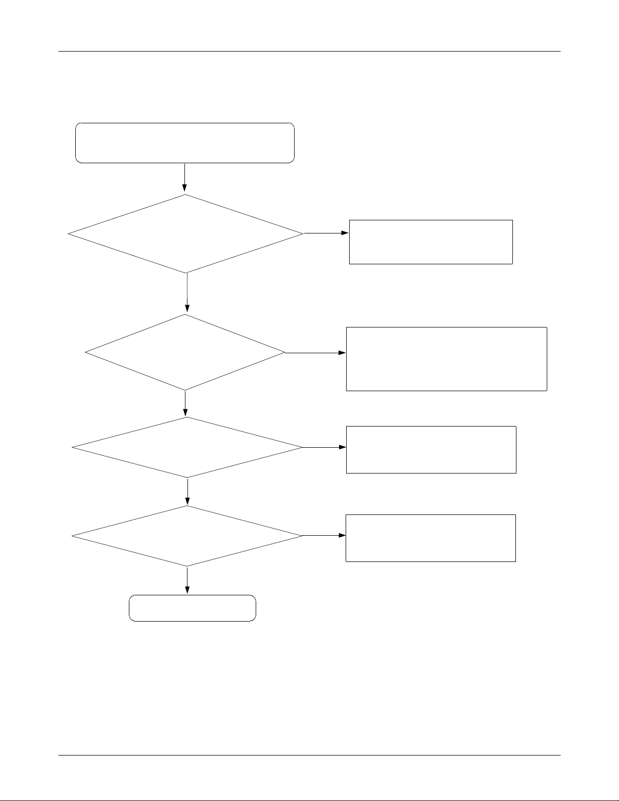
7. Flow Chart of Troubleshooting
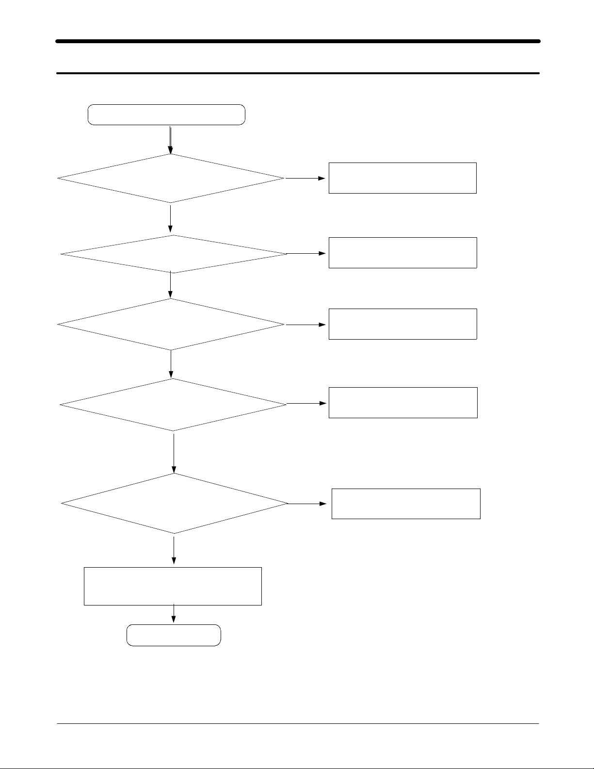
7-1. Power On
' Power On ' does not work
Yes
Check the Battery Voltage
is more than 3.4V
Yes
C424(+VDD_IO_LOW) &
C423(+VDD_IO_HIGH) = "H"?
Yes
Check the Clock at
R402=32KHZ
Yes
C400(+VDD_GSM_CORE)
=1.8V?
No
Change the Battery
No
Change the PMU (U400)
No
Resolder OSC400
No
Check the +VDD_GSM_CORE circuit
Yes
Check for the clock at C303
= 26MHz
Yes
Check the initial operation
Yes
END
SAMSUNG Proprietary-Contents may change without notice
This Document can not be used without Samsung's authorization
No
7-1
Check the clock generation circuit
(related to U100)
Page 2
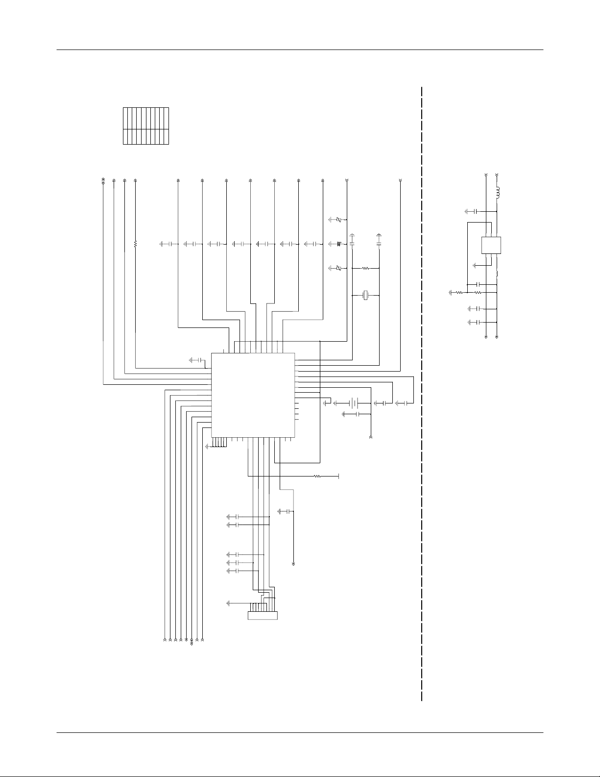
Flow Chart of Troubleshooting
VDD_IO_LOW
VDD_4V
VDD_CORE_BT
VDD_SLEEP 2.9V
1.8V
4V
MIC_BIAS
IT_PMU
SIMIO
RSTON
VDD_IO_HIGH
AVDD_HFA
AVDD
VCC_RX_TX
VCC_SYN
VDD_GSM_CORE
1.8V
2.9V
2.6V
2.8V
1.8V
2.6V
2.8V
+VDD_IO_LOW
+VDD_IO_HIGH
+AVDD_HFA
vcc
+VDD_G_A
+AVDD
+VDD_RX_TX
+VCC_SYN
VBAT
ONKEYN
DC/DC Down Conveter(1.8Volt)
V400
REF_ON
VBAT
L400
C403
C424
R409
C423
C422
M
I
I
B
S
C
A
12
R
C
_
H
T
S
11
I
Q
_
R
10
I
C
H
O
I
S
M
9
I
S
K
M
C
C
H
8
S
M
R
_
C
I
H
S
7
W
E
R
P
1
N
6
W
E
R
P
2
N
5
K
L
C
2
3
K
4
A
D
S
3
L
C
S
2
R
_
1
C
E
1
NC
54
C415
C421
13
15
14
_REC2
IOD2VBAT
IOVDD
GPO147GPO2
GND
GND
GND
GND
NC
53
49
50
51
52
48
C414
C413
23
21
22
18
17
16
HCVBAT
HCVDD
D2VDD
_SIMRSCD
SIMEN
GPO3
44
45
46
C416
C417
24
20
19
RF12VBAT
D1VDD
RF1VDD
RF2VDD
LPD1VBAT
LPVDD
C
S
O
O
25
S
O
I
C
26
K
N
O
_
Y
E
27
R
C
F
E
28
T
I
V
N
29
V
V
A
S
E
30
V
T
A
U400
SIMCKCD
B
31
H
C
V
G
32
G
H
C
V
R
D
33
C
G
H
C
/
T
R
A
U
B
X
M
A
SIMIOCD
42
43
34
V
P
C
D
D
35
B
T
A
V
P
C
36
SIMD3VBAT
SIMVCC
D3VDD
SCN
SCP
40
41
38
37
39
C412
CLOSE_THE_I/ O PIN
C409
C411
4
V
1
0
1
A
T
A
0
4
0
B
4
R
4
0
+VDD_IO_LOW
C406
C408
R402
C
S
0
O
0
4
C
C
-
V
T
7
2
1
C404
C405
C407
BU_RST
R401
5
61
4
MODE
VFB
VIN
U401
GND
RUN
SW
2
3
L401
C402
R400
C400
C401
+VDD_GSM_CORE
+VDD_IO_LOW
C420
C418
C419
SIM_CLK
SIM_RST
10
9
6
7
NC8NC
NC
VCC
I/O
NC
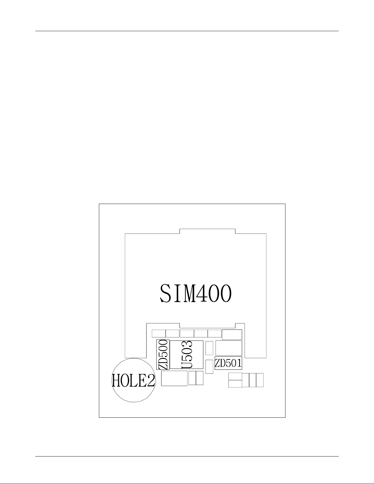
SIM400
PON_TX
REF_ON
SIMCLK
SCL
SIMRST
AUX_ON
32KHz_DIGIT
SDA
VDD_SLEEP
SIM_VCC
SIM_IO
1
2
5
3
4
VCC
RST
CLK
GND
7-2
SAMSUNG Proprietary-Contents may change without notice
This Document can not be used without Samsung's authorization
Page 3
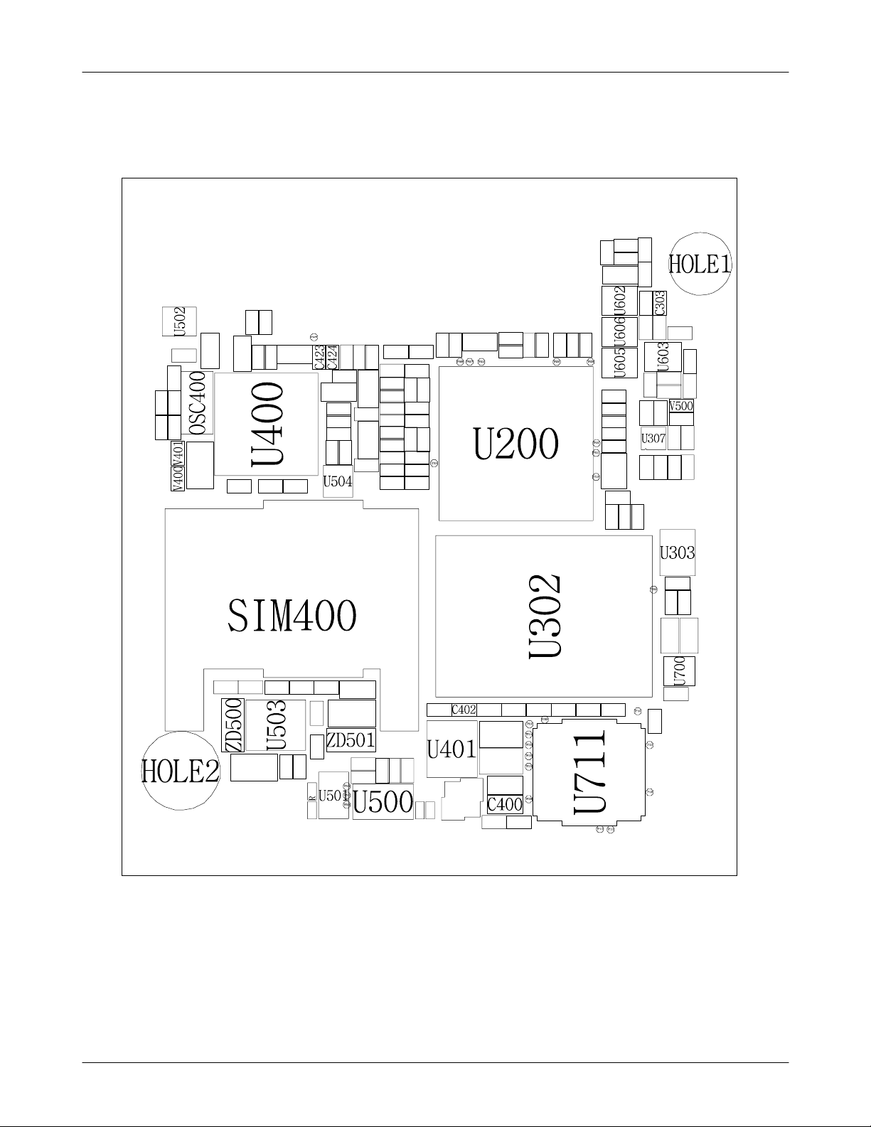
Flow Chart of Troubleshooting
7-3
SAMSUNG Proprietary-Contents may change without notice
This Document can not be used without Samsung's authorization
Page 4
Flow Chart of Troubleshooting
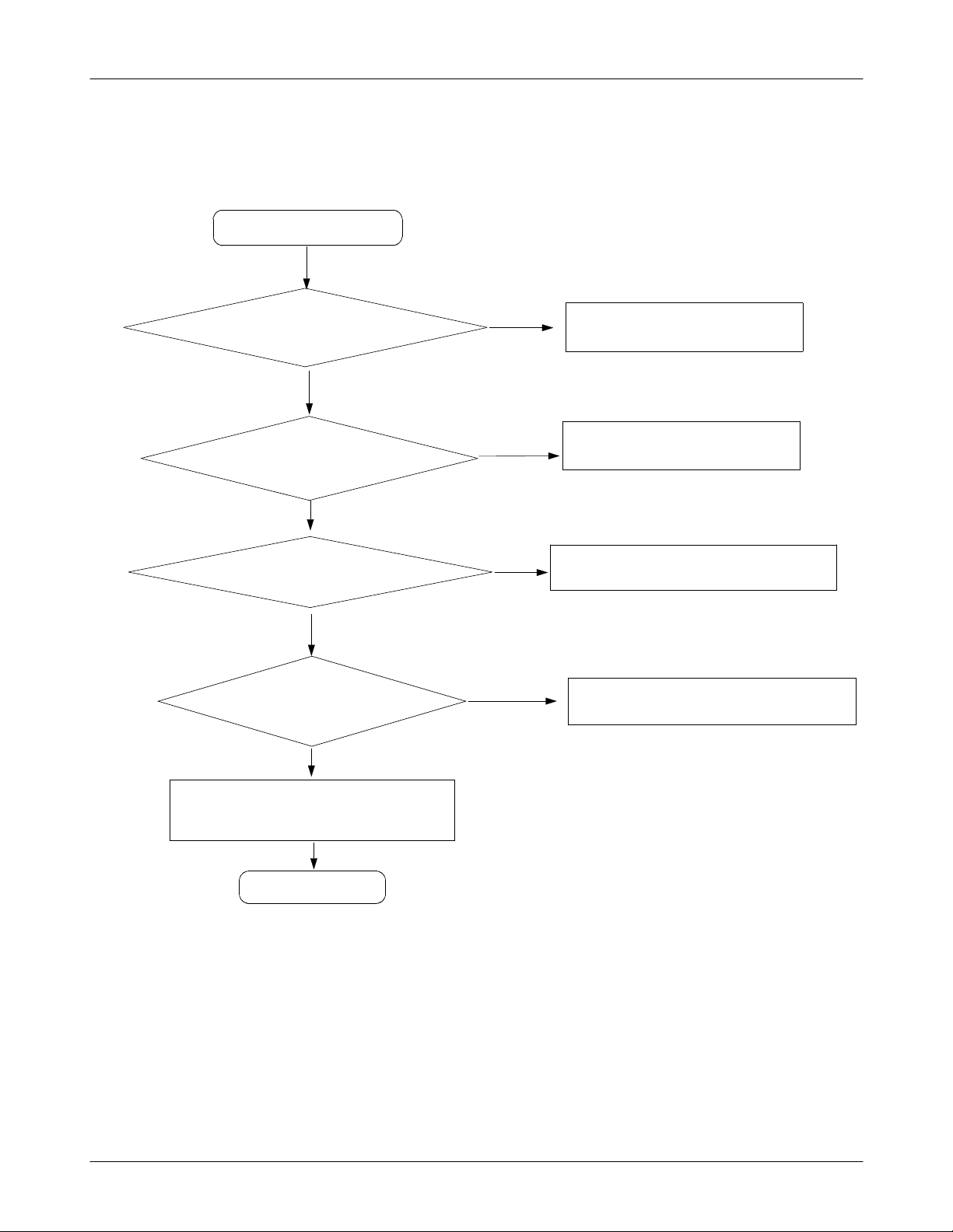
7-2. Initial
Initial Failure
Yes
Check the Battery Voltage
is more than 3.4V
Yes
U200 pin 12 (RSTON)="H"
Yes
Check U405 pin 4 : 32MHz
Yes
Is U200 R203, R204
OK?
Yes
No
No
No
No
Change the Battery
Change the PMU
Check the circuit related to reset
Check the U200
Check the 16bit data signal
Yes
END
7-4
SAMSUNG Proprietary-Contents may change without notice
This Document can not be used without Samsung's authorization
Page 5
Flow Chart of Troubleshooting
7-5
SAMSUNG Proprietary-Contents may change without notice
This Document can not be used without Samsung's authorization
Page 6
Flow Chart of Troubleshooting
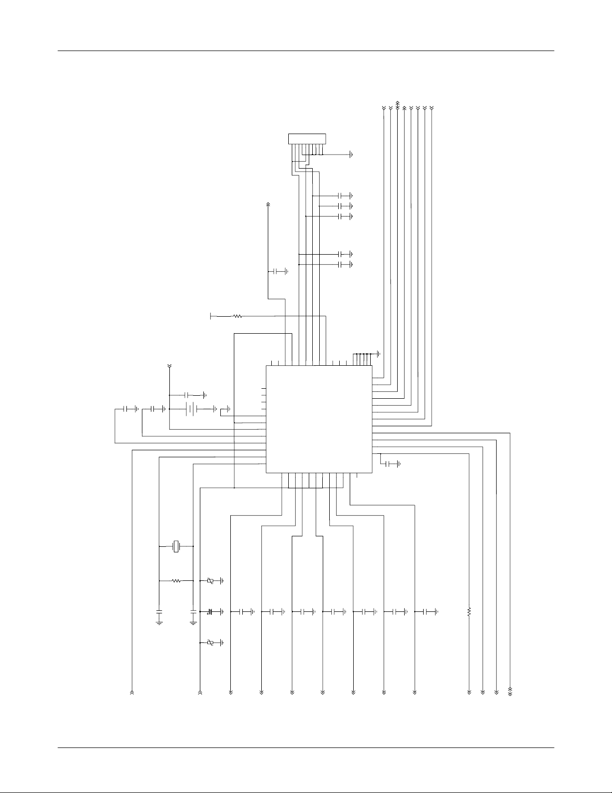
7-3. Charging Part
Abnormal charging part
Yes
Check the U503 pin 1
>4.9V
Yes
U503 pin 5 = "L"?
Yes
U503 pin 3 = "L"?
Yes
Check the U503 pin 10
≒4.2V
No
No
No
No
Check the circuit related to
V_EXT_CHARGE
Resolder or replace U503
Check the circuit related to
AUX_ON signal
Resolder or replace U503
Yes
END
7-6
SAMSUNG Proprietary-Contents may change without notice
This Document can not be used without Samsung's authorization
Page 7
+VDD_IO_HIGH
Flow Chart of Troubleshooting
V_EXT_CHARGE
R511
U503
GND
BAT
ICDL
GND
USBON
IMIN
10
9
8
7
6
R513
R514
1
CRDL
2
C507
USB
3
_PPR
4
_CHG
5
_EN
11
+VBUS
C504C503
ZD501
AUX_ON
END_OF_CHG USB_CHG_ON
CHG_ON
C501
VBAT
ZD500
BATTERY CHARGING
7-7
SAMSUNG Proprietary-Contents may change without notice
This Document can not be used without Samsung's authorization
Page 8
Flow Chart of Troubleshooting
7-4. Sim Part
Phone can't access SIM Card
SIM400 pin 1,5 = "H"?
Yes
No
Check the sim charge pump
Yes
After SIM c a rd insert,
SIM400 pin 2 = "H(SIM_RST)"?
Yes
After Power ON,
Check SIMCLK Signal on
pin3 of SIM400 in a few
Yes
Check the SIM Card
Yes
END
No
Replace PBA
No
Check the Clock
7-8
SAMSUNG Proprietary-Contents may change without notice
This Document can not be used without Samsung's authorization
Page 9
Flow Chart of Troubleshooting
SDA
32KHz_DIGIT
SIMRST
REF_ON
SCL
AUX_ON
SIM400
NC8NC
VCC
1
VDD_SLEEP
NC
RST
VCC
CLK
GND
I/O
NC
9
2
5
3
4
6
7
10
SIM_IO
SIM_RST
SIM_CLK
SIM_VCC
C419
C418
C420
SIMCLK
PON_TX
CLOSE_THE_I/ O PIN
C412
+VDD_IO_LOW
BU_RST
C407
C405
C404
B
0
4
A
0
T
4
4
0
R
40
42
41
39
38
37
SCP
SCN
D3VDD
SIMVCC
SIMD3VBAT
36
P
A
T
V
C
B
35
P
D
V
C
D
34
C
R
G
/
B
A
C
U
H
33
R
V
G
D
C
H
32
H
G
V
C
31
T
V
B
A
30
V
V
S
E
A
29
T
V
N
I
28
C
R
E
F
27
E
O
Y
_
N
K
26
O
I
S
C
25
O
O
S
C
RF12VBAT
D1VDD
RF1VDD
RF2VDD
23
21
22
24
C417
C416
46
49
50
51
52
48
44
45
43
GPO3
SIMEN
SIMIOCD
SIMCKCD
_SIMRSCD
A
X
T
M
U400
HCVBAT
HCVDD15IOD2VBAT
LPD1VBAT
LPVDD
16
18
17
20
19
53
54
NC
NC
GND
GND
GND
GND
GPO147GPO2
1
E
_
C
1
R
2
S
C
L
3
S
D
A
4
3
2
K
K
C
L
5
E
P
N
2
W
R
6
E
P
N
1
W
R
7
R
_
S
M
I
C
S
H
8
S
H
C
K
M
C
I
9
S
M
I
O
I
H
C
10
Q
_
R
I
11
C
S
_
T
H
R
12
B
I
A
S
C
M
I
_REC2
D2VDD
IOVDD
13
14
C422
1
2
7
1
V
C
A
C
T
-
O
4
S
0
C
0
R402
C406
ONKEYN
4
V
0
1
C408
C409
V400
VBAT
C411
+VDD_RX_TX
C413
+VCC_SYN
C414
+VDD_G_A
C415
+AVDD
C421
+AVDD_HFA
C423
vcc
+VDD_IO_HIGH
C424
+VDD_IO_LOW
R409
RSTON
SIMIO
IT_PMU
MIC_BIAS
7-9
SAMSUNG Proprietary-Contents may change without notice
This Document can not be used without Samsung's authorization
Page 10
Flow Chart of Troubleshooting
7-10
SAMSUNG Proprietary-Contents may change without notice
This Document can not be used without Samsung's authorization
Page 11
Flow Chart of Troubleshooting
7-5. Microphone Part
Microphone does not work
Check the connection from
MIC,
Yes
No
Resolder MIC
Yes
Check the circuit
from U200 to MIC
Yes
Check CN601, PIN 8
='H'?
Yes
Check the MIC
Yes
END
No
No
No
Resolder the
(C600, R603, R607, C603, C608)
Check the JACK_EN signal
Replace the MIC
7-11
SAMSUNG Proprietary-Contents may change without notice
This Document can not be used without Samsung's authorization
Page 12

MIC600
OSF213-42D
Flow Chart of Troubleshooting
MIC_BIAS
0
0
6
D
Z
Close to microphone
C602
C607
2
0
6
D
Z
C612
MIC_CP
C600
R600
R603
R607
Close to MCP
C603
C608
R601
C601
MIC_P
C606
MIC_N
C610
MAIN_MIC
7-12
SAMSUNG Proprietary-Contents may change without notice
This Document can not be used without Samsung's authorization
Page 13

Flow Chart of Troubleshooting
7-6. Speaker Part(Melody)
Speaker does not work
Yes
Check the U301
Pin 3, 15
Yes
Check the U600 Pin 11
(EAR1)
Yes
Check LCD
connector(CN700)
PIN 37, 38
Yes
Check LCD Module
No
Check the U301
Resolder C312, C315
No
Replace the U600
No
Resolder CN700
No
Replace LCD Module
Yes
Check speaker
SPK+, SPK-
=Operate
Yes
END
No
Replace SPK
7-13
SAMSUNG Proprietary-Contents may change without notice
This Document can not be used without Samsung's authorization
Page 14

C605
SPK_L_P
SPK_L_N
VBAT
C604
C609
R618
R602
R606
C614
C706
Flow Chart of Troubleshooting
U712
1
EN_L
24
VIPL
22
VIML
23
VREFL
18
VOPL
16
VOML
3
VDD
7
VDD
9
VDD
15
VDD
19
VDD
21
VDD
EN_R
VIPR
VIMR
VREFR
VOPR
VOMR
GND
13
12
10
11
6
4
2
VSS
5
VSS
8
VSS
14
VSS
17
VSS
20
VSS
25
26
NC
27
NC
C705
R604
R605
C613
C611
AMP_ENAMP_EN
MEL_RMEL_L
SPK_R_P
SPK_R_N
D_Class_AMP
REC+HFR_P
AUDIO_SW1
VBAT
VBAT
R608
100
R615
8
2
6
SPK_L_N
U602
1
IN
2
V+
3
GND
DG2011
COM
6
NO
5
4
NC
EARSPK_COM
HFR_N
REC-
SPK_L_P
SPK_R_N
SPK_R_P
C
0
7
9
3
2
2
6
6
6
C
C
C
L600
L601
L603
L602
CN600
1
2
3
4
spk_con
1
2
3
4
Stereo_Spk_Contact
U605
1
IN
2
V+
3
GND
1
IN
2
V+
3
GND
DG2011
U606
DG2011
COM
COM
6
NO
5
4
NC
6
NO
5
4
NC
MEL_LAUDIO_SW2
EAR1
EARSPK_L
MEL_R
EAR2
EARSPK_R
AUDIO SW
7-14
SAMSUNG Proprietary-Contents may change without notice
This Document can not be used without Samsung's authorization
Page 15

Flow Chart of Troubleshooting
7-15
SAMSUNG Proprietary-Contents may change without notice
This Document can not be used without Samsung's authorization
Page 16

7-7. Key Data Input
Check Initial Operation
When one of the keys is
pushed,
Isn'titdisplayedonLCD?
Yes
Yes
No
Flow Chart of Troubleshooting
Check the Dome sheet & Key Pad
When one of the keys is
pushed,
KEY_ROW(0,4),
KEY_COL(0,4)
signal is OK?
Yes
END
No
Resolder V702, ZD700, ZD701
7-16
SAMSUNG Proprietary-Contents may change without notice
This Document can not be used without Samsung's authorization
Page 17

Flow Chart of Troubleshooting
KEY_ROW(3)
KEY_COL(0)
KEY_ROW(3)
KEY_ROW(4)
KEY_COL(1)
0
0
7
D
Z
2
0
7
V
VOLUME_KEY
SW701
1
IN
2
OUT
3
GND
ONKEYN
SW700
SIDE-KEY
END
12
1
0
7
D
Z
CAMERA_KEY
End_Key
7-17
SAMSUNG Proprietary-Contents may change without notice
This Document can not be used without Samsung's authorization
Page 18

Flow Chart of Troubleshooting
7-18
SAMSUNG Proprietary-Contents may change without notice
This Document can not be used without Samsung's authorization
Page 19

Flow Chart of Troubleshooting
7-8. Receiver Part(<- recheck?)
Receiver does not work
Yes
U600 E AR 1, EAR 2 = 1.5V?
Yes
Check LCD connector
CN700 pin 37, 38
제목확인바람
No
Resolder U200 or change P BA
No
Resolder CN700
Yes
LCD MODULE
SPK +,- PAD = 1.5V?
Yes
END
No
Change the LCD Module
7-19
SAMSUNG Proprietary-Contents may change without notice
This Document can not be used without Samsung's authorization
Page 20

Flow Chart of Troubleshooting
7-20
SAMSUNG Proprietary-Contents may change without notice
This Document can not be used without Samsung's authorization
Page 21

7-9. Back Light (for Color Main LCD)
Backlight does not work
Yes
Is LCD Contrast set on
high level in the Menu?
Yes
Flow Chart of Troubleshooting
No
Set LCD Contrast on high lev el
IC8 pin 5 = H ?
Yes
IC8 PIN 2 ≥ Vbat ?
Yes
Replace the LCD Module
Yes
END
No
No
Change the board to board
Connector
Check the IC8 & the related circuit
7-21
SAMSUNG Proprietary-Contents may change without notice
This Document can not be used without Samsung's authorization
Page 22

Flow Chart of Troubleshooting
7-22
SAMSUNG Proprietary-Contents may change without notice
This Document can not be used without Samsung's authorization
Page 23

7-10. Key Back Light
Main Key LED does not work
U700 pin 3, 6 = "H"?
END
Flow Chart of Troubleshooting
Yes
No
Check the U200 related to "KEY_LED_ON"
Yes
7-23
SAMSUNG Proprietary-Contents may change without notice
This Document can not be used without Samsung's authorization
Page 24

Flow Chart of Troubleshooting
VBAT
U700
3
KEY_LED_ON
C704
VIN
2
GND
1
STBY
4
VOUT
5
NC
GND
6
LED , change to 0601-002055
R702
56 56
C700
LED600 LED617
56 56
LED608
R704
56
LED609
R705
R706R701
56
56
56
LED610
LED603 LED604
R708R707
56
LED611
R709
56
R710
56
LED605
R711
56
LED606
R721
R712
56
LED612
LED607 LED616LED601
R723
5656
56
LED614LED613
KEY_LED
R724R722
LED615LED602
R726
R725R703
56
56
7-24
SAMSUNG Proprietary-Contents may change without notice
This Document can not be used without Samsung's authorization
Page 25

Flow Chart of Troubleshooting
7-11. Camera part
"Camera" function does not work
Yes
Check the Camera
connector
Yes
CN 704 Pin 1, 20 = 2.8V?
Yes
CN704 Pin 17, 19 = 2.8V?
Yes
CN 704 Pin 1, 20 = 2.8V?
Yes
Check the camera module
No
Reconnect the camera module
No
Check the U405 ( or IC5)
No
Check the U405 ( or I²C)
No
Replace the Camera Module
No
Change the PBA
Yes
END
7-25
SAMSUNG Proprietary-Contents may change without notice
This Document can not be used without Samsung's authorization
Page 26

Flow Chart of Troubleshooting
7-26
SAMSUNG Proprietary-Contents may change without notice
This Document can not be used without Samsung's authorization
Page 27

7-13. BLUETOOTH
BLUETOOTH does not work
R110 = 'H'
Replace ANT102
Flow Chart of Troubleshooting
Yes
No
Check the U200
Yes
No
Replace U711
END
Yes
7-27
SAMSUNG Proprietary-Contents may change without notice
This Document can not be used without Samsung's authorization
Page 28

7-13. GSM Receiver
RX ON
RF input : 62CH
Amp : -50dBm
Yes
Flow Chart of Troubleshooting
Module1 pin8
>= -65dBm
Yes
Module1 pin1, pin2
>= -65dBm
Yes
U100
E1 >= -70dBm
F1 >= -70dBm
Yes
U100 H 7,H8,J7,J8
>= 1V
Yes
Check U200
No
Resolder CON1, C103
No No
No
Resolder C112, C108, L107
No
Check Module1
pin9,pin10,pin12 = L
Yes
Check U100
J2,A6,B6,A9,E9
>=2.7V
Yes
No
Check ANT Switch
control circuit
Resolder Module1
Check & Resolder
U100, U709
RF26MHz, RF PSU Part
Resolder U100
END
7-28
SAMSUNG Proprietary-Contents may change without notice
This Document can not be used without Samsung's authorization
Page 29

7-14. GSM Transmitter
TX ON (5Level)
Yes
Flow Chart of Troubleshooting
Module1 Pin8
>= 20dBm
No
Module1 pin11
>= 18dBm
No
U101 pin8
>= 18dBm
No
U101 7pin
>= -11dBm
No
U100 H 7,H8,J7,J8
>= 1V
Yes
Yes
Yes
Yes
No
Resolder CON1, C103
Check Module1
pin10 = H (2.68V),
pin9, pin12 = L
Yes
Resolder R122, C104, C107
Check U101
+VBAT, pin4, pin6
OK?
No
Check U100
J2,A6,B6,A9,E9
>=2.7V
Yes
No
No
Check ANT Switch
control circuit
Change or Resolder
Resolder or Change U101
Check +VBAT o r U101
control signal
Check & Resolder
U100, U709
RF26MHz, RF PSU Part
Module1
Yes
Check U200
END
Yes
Resolder U100
7-29
SAMSUNG Proprietary-Contents may change without notice
This Document can not be used without Samsung's authorization
Page 30

Flow Chart of Troubleshooting
7-15. DCS Receiver
RX ON
RF input : 698CH
Amp : -50dBm
Yes
Module1 Pin8
>= -65dBm
Yes
Module1 pin3, pin4
>= -65dBm
Yes
U100
D1 >= -70dBm
C1 >= -70dBm
Yes
U100 H 7,H8,J7,J8
>= 1V
Yes
Check U200
No
No
No
No
Resolder CON1, C103
Check Module1
pin9,pin10,pin12 = L
Yes
Resolder C106, L104, L105
Check U100
J2,A6,B6,A9,E9
>=2.7V
Yes
No
No
Check ANT Switch
control circuit
Resolder Module1
Check & Resolder
U100, U709
RF26MHz, RF PSU Part
Resolder U100
END
7-30
SAMSUNG Proprietary-Contents may change without notice
This Document can not be used without Samsung's authorization
Page 31

7-16. DCS Transmitter
TX ON (0Level)
Yes
Flow Chart of Troubleshooting
Module1 pin8
>= 20dBm
No
Module1 pin13
>= 18dBm
No
U101 pin9
>= 18dBm
No
U101 pin1
-11dBm
>=
No
U100 H 7,H8,J7,J8
>= 1V
Yes
Yes
Yes
Yes
No
Resolder CON1, C103
Check Module1
pin12 = H (2.68V),
pin9, pin10 = L
Yes
Resolder L123
Check U101
+VBAT, pin4, pin6
OK?
No
Check U100
J2,A6,B6,A9,E9
>=2.7V
OK?
Yes
No
No
Check ANT Switch
control circuit
Change or Resolder
Module1
Resolder or Change U101
Check +VBAT o r U101
control signal
Check & Resolder
U100, U709
RF26MHz, RF PSU Part
Yes
Check U200
END
Yes
Resolder U100
7-31
SAMSUNG Proprietary-Contents may change without notice
This Document can not be used without Samsung's authorization
Page 32

Flow Chart of Troubleshooting
7-17. PCS Receiver
RX ON
RF input : 661CH
Amp : -50dBm
Yes
Module1 pin8
>= -65dBm
Yes
Module1 pin5, pin6
>= -65dBm
Yes
U100
B1 >= -70dBm
A1 >= -70dBm
Yes
U100 H 7,H8,J7,J8
>= 1V
Yes
Check U200
No
No
No
No
Resolder CON1, C103
Check Module1
pin9= H
pin10, pin12 = L
Yes
Resolder C115, L109, L110
Check U100
J2,A6,B6,A9,E9
>=2.7V
Yes
No
No
Check ANT Switch
control circuit
Resolder Module1
Check & Resolder
U100, U709
RF26MHz, RF PSU Part
Resolder U100
END
7-32
SAMSUNG Proprietary-Contents may change without notice
This Document can not be used without Samsung's authorization
Page 33

7-18. PCS Transmitter
TX ON (0Level)
Yes
Flow Chart of Troubleshooting
Module1 Pin8
>= 20dBm
No
Module1 pin13
>= 18dBm
No
U101 pin9
>= 18dBm
No
U101 pin1
-11dBm
>=
No
U100 H 7,H8,J7,J8
>= 1V
Yes
Yes
Yes
Yes
No
Resolder CON1, C103
Check Module1
pin12 = H (2.68V),
pin9, pin10 = L
Yes
Resolder L123
Check U101
+VBAT, pin4, pin6
OK?
No
Check U100
J2,A6,B6,A9,E9
>=2.7V
OK?
Yes
No
No
Check ANT Switch
control circuit
Change or Resolder
Module1
Resolder or Change U101
Check +VBAT o r U101
control signal
Check & Resolder
U100, C147, U709
RF26MHz, RF PSU Part
Yes
Check U200
END
Yes
7-33
SAMSUNG Proprietary-Contents may change without notice
This Document can not be used without Samsung's authorization
Resolder U100
Page 34

Flow Chart of Troubleshooting
RAMP
DCS
R108
C125
C121
EGSM_RX_N
EGSM_RX_P
PCS_RX_N
PCS_RX_P
RF_DATA
RX_TX_QN
RX_TX_QP
RX_TX_IN
RX_TX_IP
RF_EN
R124
R122
R128
R131
G1
G2
GSM0GND
GSM0LNAI
GSM1LNAI
E1
U705
H1
GSM0LNAIB
F2
GSM1LNAIBF1GSM1GSM0GND
R127
H9
C2
B2
IOUT/IINJ7QOUT/QIN
IOUTB/IINBH7QOUTB/QINBH8LE
PCSDCSGND
PCSLNAI
U704
A1
J8
SDATA
PCSLNAIBB1PCSGND
OSC100
C137
R120
B9
F9
TXOUTDJ4TXOUTG
TCXOIN
AFC
U709
C135
23
VCON
GND
OUT
VCC
41
G8
A3
A9
B3
E9
J5
VCCLNA
VCCOPLLJ2VCCTXVCO
VCCMASH
VCCCLK
VCCBBA7VCCRFSYN
VCCBUF
VCCMIX
A6
VCCRFLO
C131
C132
C133
A8
C147
B6
VCCRFVCO
J3
VCCTXVCOG
R106
R111
+VCC_SYN
R133
R112
C127
C128
C126
H6
R105
R107
C123
C124
C122
+VDD_RX_TX
+VCC_SYN
VDD_SLEEP
C119
GND
C120
R104
6 VRAMP
GND5
VBATT4
DCS/PCSOUT910
GSMOUT
8
3
C2
E2
4
PEMD10
2
3TXEN
BAND
U101
DCS/PCSIN
GSMIN
1
7
TXON
1
2
E1
B1
Q103
B2
C1
5
6
+VDD_IO_HIGH
C117
C116
VBAT
C118
13
2
F101
L108
L123
C113
MODULE1
7
VC3
C111
2
1
3
Q102
B1
C2
E1
R102
B2
C1
E2
5
6
4
PEMD10
+VDD_IO_HIGH
L106
C104
C107
13
10
12
9
11
VC1
VC2
VC3
EGSMTX
DCS|PCSTX
ANT
G
8
C103
EGSM_RX1
EGSM_RX2
DCS_RX1
DCS_RX2
PCS_RX1
PCS_RX2
5
6
1
2
3
4
L103
C102
R101
VC2
2
3
B1 B2
C2
E2
4
5C16
PEMD10
L124
L101
L102
VC1
C100
1
E1
Q101
+VDD_IO_HIGH
J_ANT
R134
1
2
3
4
2
1
Q100
B1
C23E1
B2
C1
E2
R100
5
6
4
PEMD10
+VDD_IO_HIGH
ANT103
ANT101
G
A
C
KMS-512CON1
G
U100
DCSGSM1GND
GNDTXVCOG2
GNDTXVCOG1
GNDTXVCODH3GNDTXVCOB
GNDRFSYN
GNDMASH
GNDOPLL
GNDBUF2
GNDBUF1
GNDLNA
GNDCLK
GND
GND
GND
NC1NC
A2
H2
C9
B8
C3
E8
E2
J9
J1
2
R129
R130
CLK2CONT
DCSLNAIB
CLKOUT1
CLKOUT2
DCSLNAI
CAPQB
DIVON
CAPIB
CAPQ
CAPI
CLK
G9
A4
A5
H4
H5
C8
D1
D2
D8
D9
B5
B7
C140
C1
B4
F8
J6
C134
C136
TP100
C115
C112
L110
L109
C106
L107
L105
C108
L104
C110
C114
PCS_RX_P
DCS_RX_N
EGSM_RX_N
EGSM_RX_P
D_REF_CLK
R125
+VCC_SYN
R121
3IN2
GND
OUT
4
U703
R123
26M_DIGIT
R118
1
NC
U103
VCC
+VCC_SYN
5
C148
RF_CLK
DCS_RX_N
DCS_RX_P
PCS_RX_N
7-34
SAMSUNG Proprietary-Contents may change without notice
This Document can not be used without Samsung's authorization
C105
DCS_RX_P
Tx(DCS1800/1900)
RX(GSM900) LL
Rx(DCS1800)
Rx(PCS1900)
L
L
H
Tx(GSM900)
VC1 VC2
H
L
L
H
L
L
VC3
L(H)
L
L
L
Page 35

Flow Chart of Troubleshooting
7-35
SAMSUNG Proprietary-Contents may change without notice
This Document can not be used without Samsung's authorization
Page 36

Flow Chart of Troubleshooting
7-36
SAMSUNG Proprietary-Contents may change without notice
This Document can not be used without Samsung's authorization
 Loading...