

Page 1
2. SGH-E715 Flow Chart of Troubleshooting
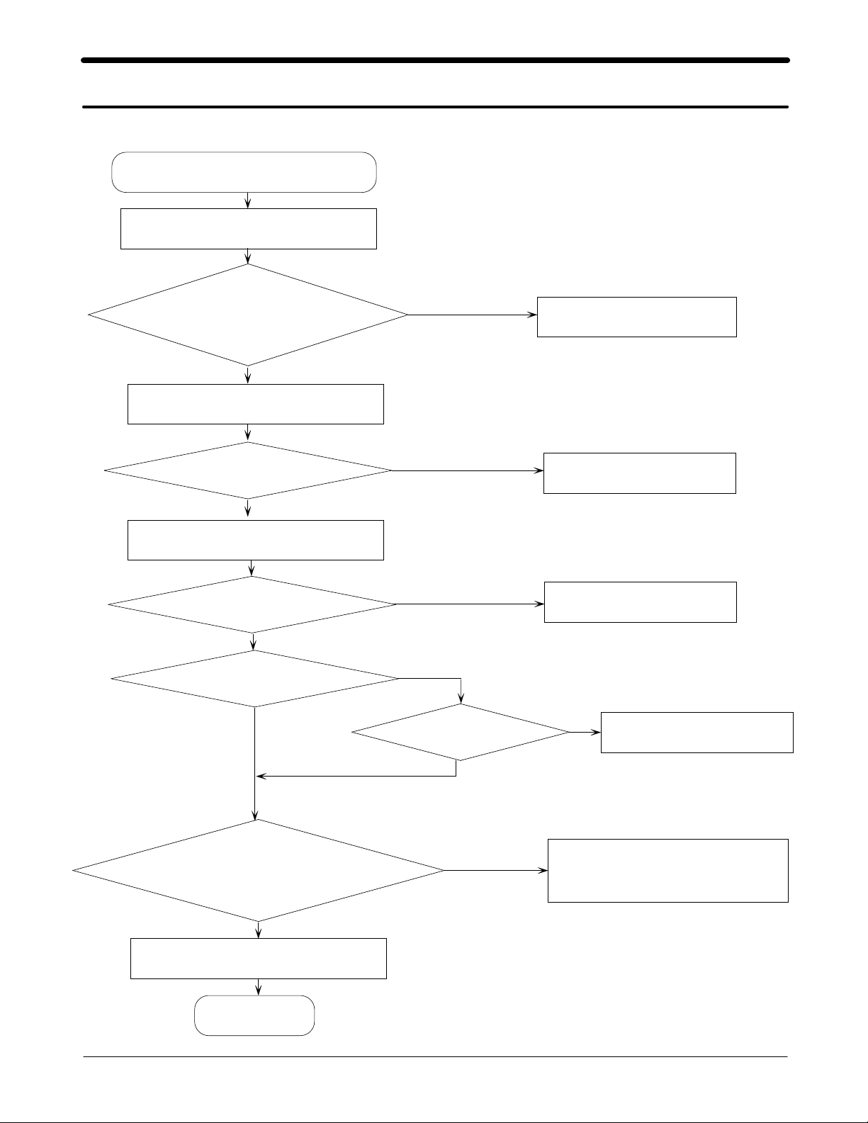
1. Power ON
'Power ON' Does not work
Check the current consumption
Current consumption
≥100mA ?
YES
Check the V bat. voltage
Voltage ≥ 3.3V ?
YES
Check the pin of U100
pin #11 ≥ 2.8V ?
YES
pin #39 and #33 = 2.8V
NO
NO
NO
NO
Down load again
Charge the Battery
Check U100 and C110
YES
Check the clock signal
at pin #3 of OSC400
Freq.=13MHz,Vrms 300mV
YES
Check the Initial operation
END
SAMSUNG Proprietary-Contents may change without notice
This Document can not be used without Samsung's authorization
Pin #9=1.8V?
YES
NO
2-1
NO
Check U100 and C109
Check the clock generation
circuit (OSC400, U402 pin#4)
Page 2
SGH-E715 Flow Chart of Troubleshooting and Circuit Diagrams
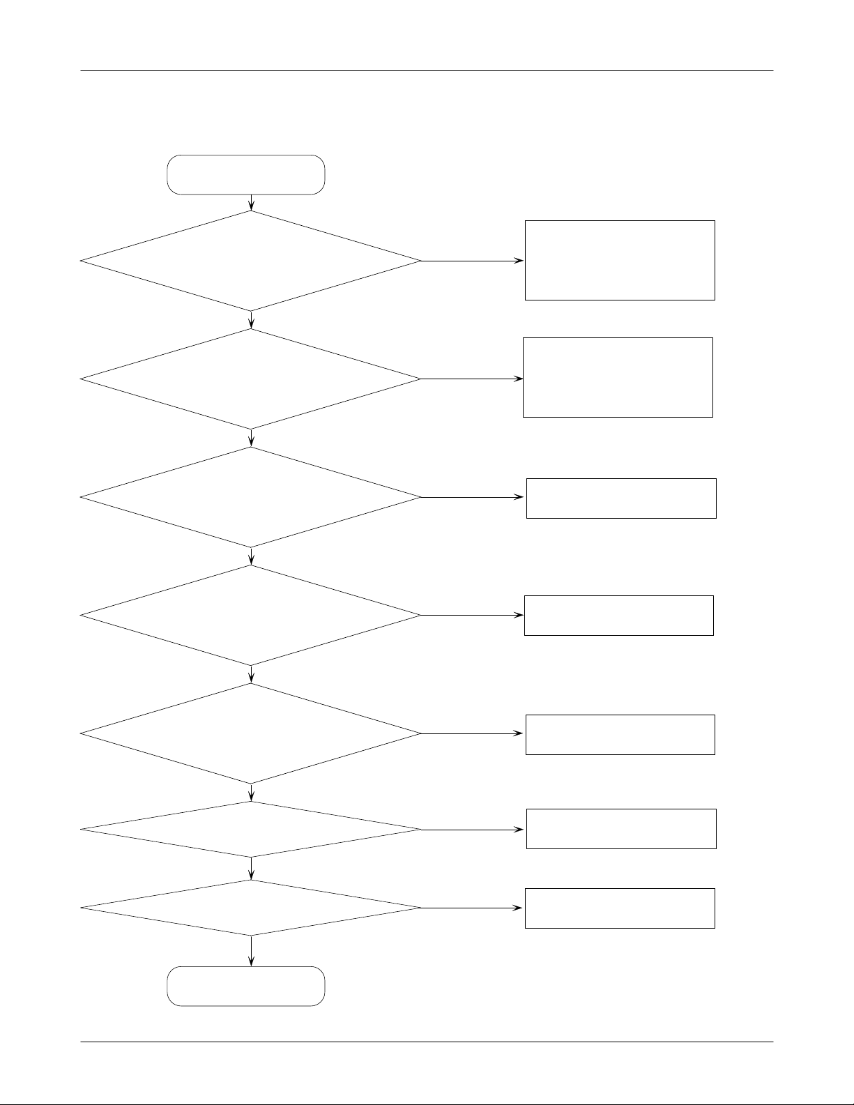
2. System Initial
Initial Failure
The pin #9 of U100 = 1.8V
and pin #11 of U100=2.8V?
YES
Is the pin #19 of U100
" Low --> High" ?
YES
There is 32.768KHz wave
form at the C324, C325 ?
YES
Is the pin #25 of U100
is High ?
NO
NO
NO
NO
Check the U100
(If it has some problem,
it has to be replaced.)
Check the U100
(If it has some problem,
it has to be replaced.)
Check the U303
Check the U300
YES
The voltage is "High"
at the C106,C112,C113 ?
YES
LCD Display OK ?
YES
Sound operation OK ?
YES
END
SAMSUNG Proprietary-Contents may change without notice
This Document can not be used without Samsung's authorization
NO
NO
NO
2-2
Check the U100
Check the LCD part
Check the Audio part
Page 3
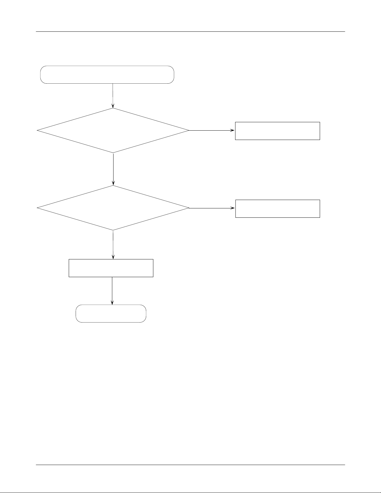
3. SIM Part
"Insert SIM" is displayed on the LCD
SGH-E715 Flow Chart of Troubleshooting and Circuit Diagrams
Is there any signal
pin #52,53,54 of U100 ?
YES
Is there any signal
pin #1,2,3,6 of CN100 ?
YES
Check the SIM Card
NO
Check the U303
NO
Check the U100
END
2-3
SAMSUNG Proprietary-Contents may change without notice
This Document can not be used without Samsung's authorization
Page 4
SGH-E715 Flow Chart of Troubleshooting and Circuit Diagrams
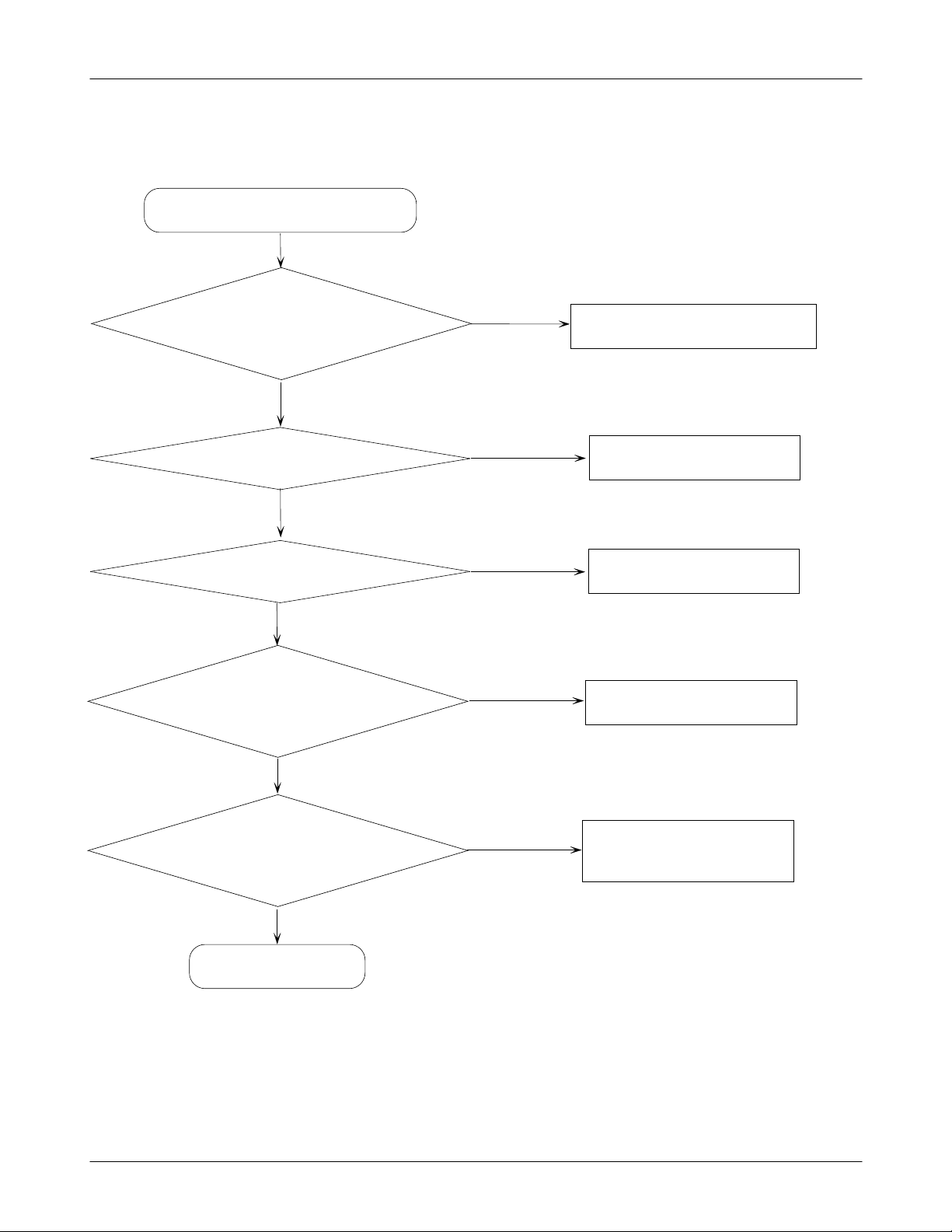
4. Charging Part
Abnormal charging operation
The pin #17,18 of CN101
(VEXT) is 5V ?
YES
The pin#2 of U102 is Low?
YES
The pin#3 of U102 is Low?
YES
The pin#5 of U101 is
3.2~4.2V?
NO
NO
NO
NO
Replace TA or check CN101
Check the U102
Check the U102
Check the U101
YES
The ICHRG =1V(during charging)
&180mV(fullcharging)?
YES
END
SAMSUNG Proprietary-Contents may change without notice
This Document can not be used without Samsung's authorization
2-4
NO
Solder again or change
R119
Page 5
RTCALAR M
PWR_KEEP
KEY_COL(2)
KEY_ROW(0)
TA_VEXT
CHG_DET
PWR_O N
JIG_ON
3
2
VRTC
R11 0
390K
Q102
DTC144EM
C103
470N F
C105
100N F
1
Q100
SGH-E715 Flow Chart of Troubleshooting and Circuit Diagrams
CN100
1
4
1
4
2
5
2
5
6
3
3
6
G
G
GG
7
89
54
53
52
44
45
56
3
2
1
43
46
47
13
21
20
14
15
16
17
18
22
23
24
25
26
27
55
57
58
59
60
C117
10UF
10V
10
49
UP_RST
UP_CLK
UP_IO
ADC_AUX1
ADC_AUX2
ADC_TRIG
VACC
VBA T
VEXT
BTEM P
PWR_SW1N
PWR_SW 2
RTC_ALM N
PWR_KEEP
PSW1_BUF
INTRQ
SDI
SDO
SCLK
CSN
EN_3
EN_4[0]
EN_4[1]
EN_5
EN_5A
EN_5B
RING_PW M
GN D
GN D
GN D
GNDD
D
N
G
2
1
6
6
D
N
G
3
6
C102
C101
33PF
33PF
SIMRST
SIMCLK
SIMDATA
VBAT
TA_VEXT
R114
UP_SDI
330K
UP_SCLK
UP_CS
EN_VRF
EN_VPAC
XOEN A
R118
CHG_O N
10K,1%
1
3
2
C100
33PF
C104
100NF
30
48
50
51
T
K
I
M
O
S
L
I
S
_
R
C
V
_
_
M
I
M
M
I
I
S
S
S
U100
R
V
V
D
R
_
D
G
_
D
D
N
B
N
N
I
I
V
R
G
G
4
5
4
6
U103
1
2
3
6
28
29
F
F
1
Q
E
E
D
D
R
R
D
N
V
C
N
G
VLDO_7
G
VDD67
VLDO_6
VL5S_A
VL5S_B
VLDO_5
VDD5
VL4S_A
VL4S_B
VLDO_4
VDD34
VLDO_3
VRTC
VLDO_2
RESETN
VLDO_1
VDD12
V
V
R
R
D
D
_
_
1
D
E
L
78
1
2
6
5
4
2
D
E
L
ISENSE
GND
VCC
U101
D
N
G
5
6
6
6
DRIVE
VSENSE
PRO G
R120
47K,1%
D
D
D
N
N
N
G
G
G
8
7
6
6
BACKLIGHT2
BACKLIGHT1
6
5
4 3
VBA T
VREF
40
41
42
32
31
33
34
36
35
37
38
39
12
11
19
9
10
C107
10U F
10V
Q101
6
5
2
4
1
3
TA_VEXT
R121
3K
C108
470NF
C109
2.2UF
R119
10K,1%
VBAT
VCC D VCC_1.8A
VRF
C110
2.2U F
C116
10U F
10V
C106
2.2U F
ICHRG
VPAC
C111
2.2U F
VOSC
C112
2.2U F
VCC A
10U F
C113
VCC B
C114
2.2U F
10V
C115
100PF
VRTC
S
O
P
G
E
N
R115
1.2K
1
2
RST
M1
2-5
SAMSUNG Proprietary-Contents may change without notice
This Document can not be used without Samsung's authorization
Page 6

5. Microphone Part
Micro-phone does not work
SGH-E715 Flow Chart of Troubleshooting and Circuit Diagrams
Is the assembled status of
Microphone O.K?
YES
Check the DC bias voltage on
Mic path.
The voltage of C237 is
2.2V±10%?
YES
Is microphone OK?
NO
NO
NO
Reassemble the microphone
Solder the microphone again
or Replace
C230,C237,R217,R218,R219
Check U300
YES
END
2-6
SAMSUNG Proprietary-Contents may change without notice
This Document can not be used without Samsung's authorization
Page 7

SGH-E715 Flow Chart of Troubleshooting and Circuit Diagrams
6. Speaker Part
There is no sound from speaker
Is the terminal of speaker
is O.K?
YES
Are there any signal
at the pin #40,42 of CN200?
YES
YES
Are there any signal
at the pin #5,7 of U201?
NO
NO
Thetypeofsoundfrom
the speaker is Melody?
NO NO
Replace the speaker
Check the LCD module
& Replace CN200
NO
Are there any signal
at the pin #3,9 of U201?
YES
Pin #4 of U201
is Low?
YES
Check U202
SAMSUNG Proprietary-Contents may change without notice
This Document can not be used without Samsung's authorization
NO
Check
U201,
U303
END
2-7
YES
NO
Pin #4 of U201
is High?
YES
Check U300
Page 8

SGH-E715 Flow Chart of Troubleshooting and Circuit Diagrams
1
0
2
N
3
N
_
K
P
S
_
R
A
0
K
E
2
0
2
0
1
R
A
C
C
V
4
4
0
0
2
F
1
1
C
2
6
5
4
1
P
P
N
_
N
_
_
I
C
I
K
_
C
I
P
K
M
M
S
_
C
_
_
R
A
R
R
J
A
A
A
E
E
E
0
6
2
2
R
H
1
3
n
0
0
2
0
1
L
3
2
2
0
0
2
H
T
F
2
P
4
0
2
8
1
C
2
0
2
D
Z
4
4
2
F
C
P
8
0
2
6
2
5
R
1
F
4
P
2
3
C
3
C
F
4
N
P
3
3
2
3
R
1
0
2
D
Z
7
F
4
P
2
3
3
C
0
0
2
D
Z
6
F
4
2
N
C
1
5
F
4
P
2
2
C
8
3
0
2
D
Z
8
F
4
N
2
1
C
K
3
1
3
2
R
9
F
4
2
N
1
C
2
3
2
K
1
R
H
H
n
4
2
0
n
2
2
0
0
2
2
1
0
R
R
1
F
6
V
3
U
3
2
3
.
3
C
6
C
I
M
_
N
I
A
M
5
H
0
n
0
0
2
0
L
1
0
F
3
U
2
1
C
7
K
1
0
2
1
R
N
I
C
I
M
F
3
P
2
3
3
C
2
F
3
2
N
1
C
F
1
K
P
4
2
7
.
2
8
3
4
2
R
C
8
3
2
C
A
C
C
V
9
K
1
2
.
2
1
R
0
F
6
P
2
9
3
C
8
1
%
2
1
,
R
K
7
4
F
3
P
3
9
2
3
C
T
U
O
C
I
M
F
7
3
U
2
3
3
C
F
0
4
U
2
3
3
C
P
N
N
I
B
B
_
T
T
K
U
U
C
O
O
A
A
A
J
K
7
3
.
2
4
2
R
F
n
0
7
4
9
F
3
U
2
1
C
5
K
2
0
2
1
R
N
I
X
U
A
8
9
7
3
3
3
2
2
2
R
R
0
R
0
V
3
.
6
1
3
2
R
D
C
C
V
0
3
2
R
A
C
C
V
1
F
6
P
2
9
C
3
7
%
2
1
2
,
R
K
7
4
3
F
4
P
2
9
3
C
T
U
O
X
U
A
C
C
N
F
9
P
2
0
2
2
R
0
8
H
C
T
I
W
S
_
R
A
E
K
1
3
%
1
,
K
2
8
N
0
1
4
4
2
2
R
R
1
0
0
2
Q
2
5
3
K
2
1
R
5
2-8
SAMSUNG Proprietary-Contents may change without notice
This Document can not be used without Samsung's authorization
Page 9

7. Camera Part
Camera function does not work
SGH-E715 Flow Chart of Troubleshooting and Circuit Diagrams
Check the connect CN200?
YES
Pin #9 of U203 = 2.8V?
YES
Pin #10 of U203 = 2.8V?
YES
Pin#3 of OSC200 is 25MHz?
YES
NO
NO
NO
NO
Connect the CN200
Check the U203
YES
Pin #2 of U203 = High?
Pin#1 of OSC200 = High?
YES
NO
NO
Check
U303
Check
U200
Pin#54 of CN200 is High?
END
SAMSUNG Proprietary-Contents may change without notice
This Document can not be used without Samsung's authorization
Replace the OSC200
NO
Check solder status of
R207, C208
2-9
Page 10

SGH-E715 Flow Chart of Troubleshooting and Circuit Diagrams
8. EGSM Receiver
Continuous RX ON
RF Input : 62 CH
AMP : -50dBm
NORMAL CONDITION
Catch the channel ?
YES
F400 Check
Pin #6 ≥ -65dBm ?
YES
F400 Check
Pin #11 ≥ -65dBm ?
YES
F403 Check
Pin #1 ≥ -65dBm ?
YES
U401 Check
Pin#20,21 ≥ -65dBm ?
YES
NO
NO
NO
NO
NO
Check soldered status of
C400,402
CN400
Resolder or Change
F400 Resolder or Change
Check soldered status of
F400 Resolder or Change
Check soldered status of
L410 &
C415,417,L406,F403
U401 Check
Pin#9,32=Clean 2.8V?
YES
U401 Check
Pin#28,1,2,3=100mV?
YES
Check U300
NO
U100,C106,C112
Check or resolder
NO
U401 Check
Pin #8 : 13MHz ?
Vpp : 860mV?
NO
OSC400 Check
Pin #8 : 13MHz ?
Vpp : 950mV?
NO
YES YES YES
U401
Change or resolder
2-10
R412,C426
resolder
SAMSUNG Proprietary-Contents may change without notice
This Document can not be used without Samsung's authorization
OSC400 Check
Pin #4 = 2.8V ?
OSC400
Change or resolder
NO
Page 11

9. EGSM Transmitter
SGH-E715 Flow Chart of Troubleshooting and Circuit Diagrams
F400 Pin#6
About 2~3 dBm?
YES
C402,CN400
Check & Change
U400 Pin #6 is
YES
About -5 dBm?
NO
NO
C403
=3.7V?
YES
Level of
1.2V?
YES
U400 pin#7
NO
F400
Pin#10 = High?
Level of
F400 Pin#7 is
4~5dBm ?
F400
Check & Change
NO
NO
YES
YES
Check the
Battery Block
Check
&ChangeR406
OK ?
YES
NO
Check & Change
U300,301
NO
Continuous TX ON condition
TX Power Code : 500 code Applied
U300
Check & Change
CH : 62
RBW : 100KHz
VBW : 100KHz
SPAN : 10MHz
REF. Level : 10dBm
ATT. : 20dB
NO
U400 pin#3
High ?
YES
Change U400
U401 Check
Pin#9,32 ≥ 2.8V ?
YES
U401 Check
Pin #8 : 13MHz ?
Vpp : 860mV?
YES
U401 Pin
#4,5,6,7 = 1.7V?
YES
Change U400Check U300
NO
Check U300
NO
NO NO
U100,C106,C112
Check or resolder
OSC400 Check
Pin #8 : 13MHz ?
Vpp : 950mV?
YES YES
R412,C426
resolder
OSC400 Check
Pin #4 = 2.8V ?
OSC400
Change or resolder
NO
2-11
SAMSUNG Proprietary-Contents may change without notice
This Document can not be used without Samsung's authorization
Page 12

SGH-E715 Flow Chart of Troubleshooting and Circuit Diagrams
10. PCS Receiver
Continuous RX ON
RF Input : 660 CH
AMP : -50dBm
NORMAL CONDITION
Catch the channel ?
YES
F400 Check
Pin #6 ≥ -65dBm ?
YES
F400 Check
Pin #3 ≥ -65dBm ?
YES
F401 Check
Pin #1 ≥ -65dBm ?
YES
U401 Check
Pin#16,17 ≥ -65dBm ?
YES
NO
NO
NO
NO
NO
Check soldered status of
C400,402
CN400
Resolder or Change
F400 Resolder or Change
Check soldered status of
L408,C429
Check soldered status of
C405,406,L402,F401
U401 Check
Pin#9,32=Clean 2.8V?
YES
U401 Check
Pin#28,1,2,3=100mV?
YES
Check U300
NO
U100,C106,C112
Check or resolder
NO
U401 Check
Pin #8 : 13MHz ?
Vpp : 860mV?
NO
OSC400 Check
Pin #8 : 13MHz ?
Vpp : 950mV?
NO
YES YES YES
U401
Change or resolder
2-12
R412,C426
resolder
SAMSUNG Proprietary-Contents may change without notice
This Document can not be used without Samsung's authorization
OSC400 Check
Pin #4 = 2.8V ?
OSC400
Change or resolder
NO
Page 13

11. PCS Transmitter
SGH-E715 Flow Chart of Troubleshooting and Circuit Diagrams
F400 Pin#6
About 2~3 dBm?
YES
C402,CN400
Check & Change
U400 Pin #6 is
YES
About -5 dBm?
NO
NO
C403
=3.7V?
YES
Level of
1.2V?
YES
U400 pin#1
NO
F400
Pin#4 = High?
Level of
F400 Pin#5 is
4~5dBm ?
F400,L403,C413
Check & Change
NO
NO
YES
YES
Check the
Battery Block
Check
&ChangeR406
OK ?
YES
NO
Check & Change
U300,302
NO
Continuous TX ON condition
TX Power Code : 350 code Applied
U300
Check & Change
CH : 660
RBW : 100KHz
VBW : 100KHz
SPAN : 10MHz
REF. Level : 10dBm
ATT. : 20dB
NO
Check U300
U400 pin#3
High ?
YES
Change U400
U401 Check
Pin#9,32 ≥ 2.8V ?
YES
U401 Check
Pin #8 : 13MHz ?
Vpp : 860mV?
YES
U401 Pin
#4,5,6,7 = 1.7V?
YES
Change U400
NO
Check U300
NO
NO NO
U100,C106,C112
Check or resolder
OSC400 Check
Pin #8 : 13MHz ?
Vpp : 950mV?
YES
R412,C426
resolder
OSC400 Check
Pin #4 = 2.8V ?
YES
OSC400
Change or resolder
NO
2-13
SAMSUNG Proprietary-Contents may change without notice
This Document can not be used without Samsung's authorization
Page 14

SGH-E715 Flow Chart of Troubleshooting and Circuit Diagrams
N
P
P
N
P
I
I
Q
Q
I
X
X
X
X
X
R
T
R
R
R
F
8
N
2
0
4
0
1
C
F
R
V
N
N
I
I
_
_
M
M
A
A
P
P
_
_
S
M
C
S
P
G
D
1
T
N
A
H
0
n
0
T
6
4
.
N
5
L
A
H
0
n
0
0
4
.
1
C
1
0
F
4
P
1
C
4
2
G
1
0
3
G
0
4
N
C
F
2
0
P
4
7
4
C
0
0
4
0
R
1
5
8
7
6
3
2
1
3
4
3
G
N
D
3
3
N
D
G
2
3
V
D
D
1
3
N
D
G
0
G
N
D
3
9
N
D
G
2
8
P
Q
2
7
2
T
6
2
N
E
5
2
2
4
1
2
3
2
G
2
D
2
0
0
4
F
N
I
N
I
_
_
M
M
A
A
P
P
_
_
S
M
C
S
P
G
D
4
1
0
0
4
4
0
0
R
R
2
2
2
8
3
0
4
5
1
R
5
2
0
0
4
4
0
R
R
2
8
4
3
3
3
D
D
C
C
N
P
P
N
I
I
I
N
N
N
N
Q
X
X
X
G
G
X
T
R
R
R
R
X
1
0
4
U
U
X
O
X
D
I
A
G
D
I
A
G
O
R
F
N
P
P
N
N
D
D
P
G
G
I
I
I
I
I
O
R
F
F
F
F
F
F
R
R
R
R
R
7
8
9
0
1
1
1
1
2
2
P
P
N
N
N
_
_
_
_
_
N
N
N
N
N
I
I
I
I
I
_
_
_
_
_
A
A
A
A
A
N
N
N
N
N
L
L
L
L
L
_
_
_
_
_
S
S
S
M
M
C
C
C
S
S
P
D
D
G
G
P
N
_
_
N
N
N
I
I
_
_
_
N
A
A
I
N
_
N
L
L
A
_
_
N
S
S
L
C
C
_
P
P
S
C
D
H
2
n
0
6
4
.
L
5
F
P
8
F
5
.
6
0
4
C
1
0
4
F
2
8
6
9
0
7
2
F
P
1
0
8
7
4
P
.
0
2
C
1
.
4
2
C
3
4
3
1
T
T
T
T
U
U
O
U
G
O
O
G
5
2
2
0
N
4
I
F
1
F
9
P
2
5
4
.
0
C
H
F
F
8
9
0
n
0
0
1
P
P
5
4
4
4
.
2
7
L
1
2
L
L
4
1
1
1
3
X
X
X
G
R
R
R
M
S
S
S
C
C
G
0
V
C
3
1
P
D
G
E
V
C
2
4
X
T
G
X
S
T
N
A
C
M
C
1
V
2
P
/
S
S
G
C
E
D
5
7
1
3
C
4
F
P
4
3
0
0
4
4
L
L
0
F
0
P
1
5
4
.
0
C
H
1
n
0
7
4
.
2
L
8
0
4
F
C
P
5
7
.
0
F
R
_
M
3
P
N
1
N
K
Q
Q
I
L
X
X
X
T
C
T
T
F
6
1
P
4
F
0
8
C
0
1
U
1
4
1
C
F
R
V
7
6
5
P
N
N
I
Q
Q
X
X
X
T
T
T
8
X
I
N
V
D
D
P
D
N
_
S
D
O
S
E
N
_
K
C
L
S
I
S
D
P
P
D
I
N
F
G
R
5
6
1
1
P
_
N
I
_
A
N
L
_
S
C
P
P
_
N
I
_
A
N
L
_
S
C
D
H
5
n
0
8
4
.
6
L
F
4
P
1
2
4
.
2
C
4
T
U
O
G
5
G
2
N
I
1
0
3
C
4
N
C
N
N
N
E
E
E
_
_
_
X
X
X
T
T
R
_
_
_
S
S
M
C
C
S
D
P
G
1
C
N
F
9
1
N
4
2
C
2
9
0
1
1
1
2
1
3
1
4
1
T
K
N
E
L
L
E
A
_
R
C
D
I
E
R
R
S
S
E
E
S
S
N
P
_
_
N
N
I
I
_
_
A
A
N
N
L
L
_
_
M
M
S
S
G
G
H
6
0
n
4
7
2
L
F
P
F
5
P
7
7
5
5
.
1
1
7
0
4
.
4
C
0
C
3
4
T
T
U
U
O
O
5
G
2
3
G
0
N
4
I
F
1
1
3
4
C
C
N
1
9
7
1
1
0
T
N
4
I
U
0
0
4
U
C
A
P
V
T
A
B
V
3
F
0
U
4
V
0
3
C
.
0
6
1
F
4
0
N
4
0
1
C
1
S
3
O
F
C
S
R
D
C
P
C
C
V
2
2
D
C
C
V
2
N
1
3
8
G
V
C
C
1
P
T
0
D
M
T
G
N
1
N
A
E
A
E
A
R
R
B
X
V
V
V
B
T
6
3
2
5
4
2
F
1
4
N
1
C
K
6
0
0
0
4
1
R
F
1
1
P
4
3
C
3
F
9
P
0
0
4
7
C
2
N
L
R
E
_
E
E
X
S
W
_
T
O
D
P
N
X
A
T
B
_
X
T
2-14
SAMSUNG Proprietary-Contents may change without notice
This Document can not be used without Samsung's authorization
 Loading...