Samsung DVD-P181 Schematic
7. Schematic Diagrams
7-1 All block Diagram ----------------------------------------------------------------------------------------7-2
7-2 Power ------------------------------------------------------------------------------------------------------------7-3
7-3 S.M.P.S (S.M.P.S PCB) ----------------------------------------------------------------------------------7-5
7-4 Front Key (S.M.P.S PCB) ------------------------------------------------------------------------------7-6
7-5 Video (Main PCB) -----------------------------------------------------------------------------------------7-7
7-6 Audio (Main PCB) -----------------------------------------------------------------------------------------7-8
7-7 Memory (Main PCB) -------------------------------------------------------------------------------------7-9
7-8 Decoder (Main PCB) -----------------------------------------------------------------------------------7-10
7-9 Power (Main PCB) --------------------------------------------------------------------------------------7-11
Note
● For schematic Diagram
- Resistors are in ohms, 1/8W unless otherwise noted.
Special note :
Most semiconductor devices are electrostatically sensitive and therefore require the special handling techniques
described under the "electrostatically sensitive (ES) devices" section of this service manual.
Note :
Do not use the part number shown on this drawing for ordering. The correct part number is shown in the parts list
(may be slightly different or amended since this drawing was prepared).
Important safety notices :
Components identied with the mark have the special characteristics for safety. When replacing any of these
components. Use only the same type.
7-10 Connector (Power Key PCB)- -------------------------------------------------------------------7-12
7-11 Power Key (Power Key PCB) -------------------------------------------------------------------7-13
7-12 Scart (Scart PCB) -------------------------------------------------------------------------------------7-14
7-13 Scart Connector (Scart PCB) -------------------------------------------------------------------7-15
7-14 Karaoke (Karaoke PCB) --------------------------------------------------------------------------7-16
Samsung Electronics This Document can not be used without Samsung's authorization 7-1
Schematic Diagrams
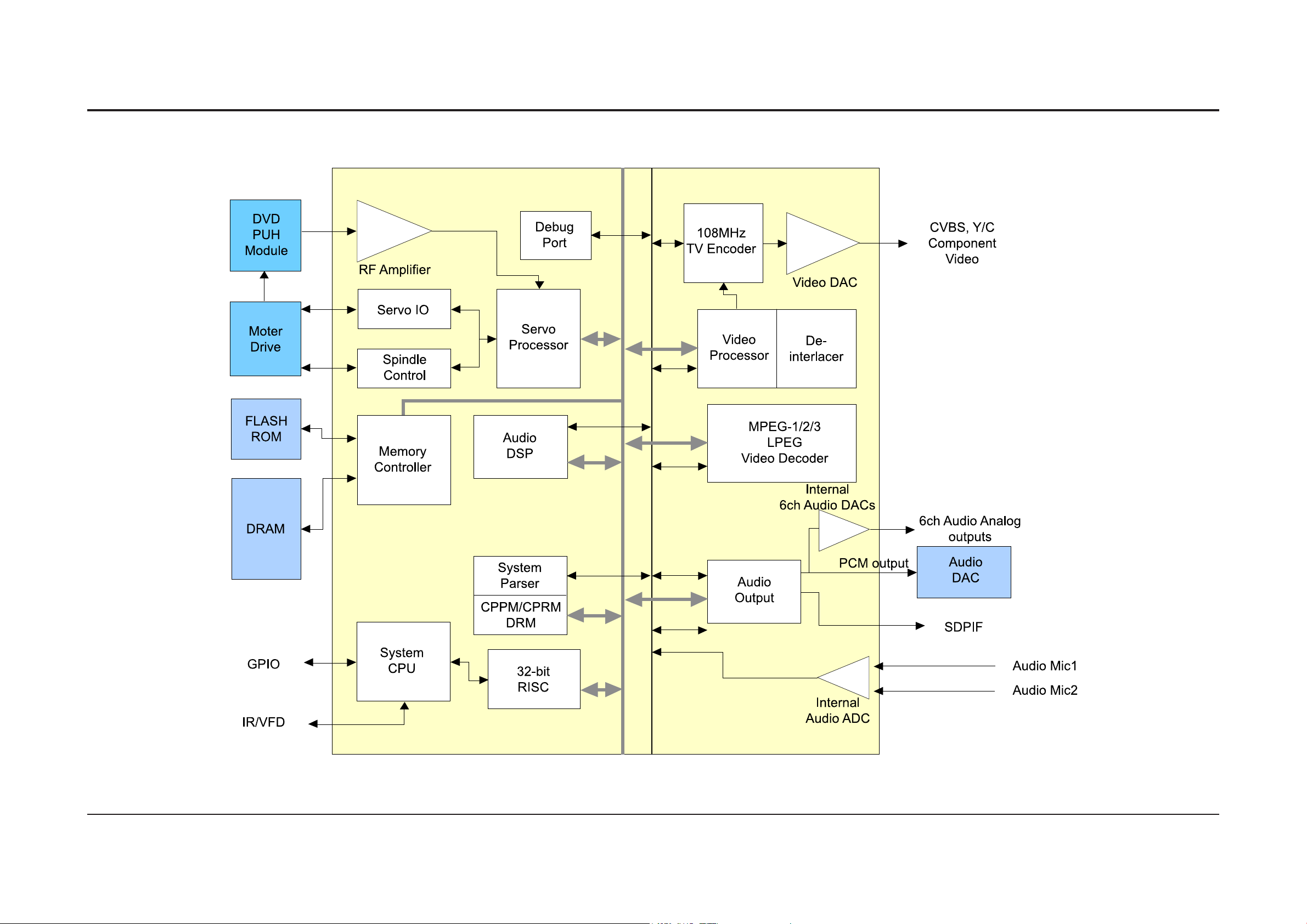
7-1 All block Diagram
7-2 This Document can not be used without Samsung's authorization Samsung Electronics
7-2 Power
Schematic Diagrams
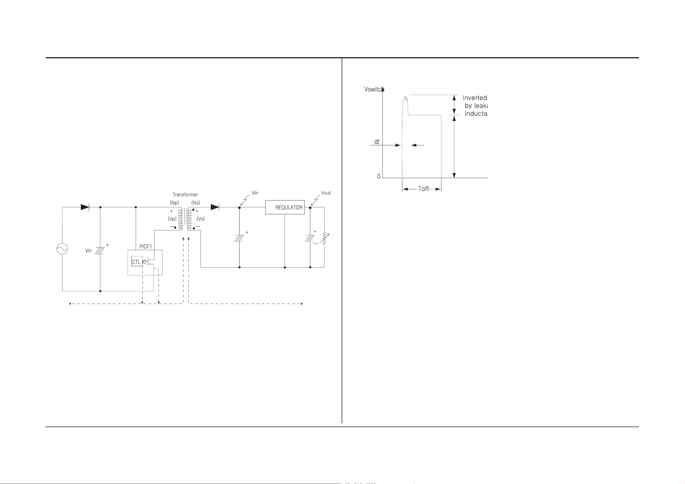
7-2-1 About S.M.P.S (Ringing Choke Converter Method)
u Terms
1) 1st : Common power input to 1st winding.
2) 2nd : Circuit followings output winding of transformer.
3) f (Frequency) : Switching frequency (T : Switching cycle)
4) Duty : (Ton/T) x 100
7-2-2 Circuit description [FLY-Back RCC(Ringing Choke Converter)] Control
(a) AC Power Rectication/Smoothing Terminal
1) PDS01, PDS02, PDS03, PDS04 : Convert AC power to DC(Full wave rectication).
2) PEF10 : Smooth the voltage converted to DC.
3) PCD01, PCD02, PBS01 : Noise removal at power input/output.
4) PVA1 : SMPS protection at power surge input.
(b) SNUBBER Circuit :
PDS11, PCD12, PRS13, PCD11, PPS12
1) Prevent residual high voltage at the terminals of
switch during switch off/Suppress noise.
High inverted power occurs at switch (PQR11) off,
because of the 1st winding of transformer :
(V=-L1 xdi/dt. L1 : Leakage Induction)
A very high residual voltage exist on both terminals
of PICF1 4, 5~8pin because dt is a very short.
2) SNUBBER circuit protects PQR11 from damage
through leakage voltage suppression by RC,
(Charges the leakage voltage to PDS11, PER13,
PCD12 and discharges to PRS11, PRS12).
Fig. 7-2
(c) Driving circuit
When Vin supplied, driving current Ig occurs throuhg the PICF1. By this I1 (=Hfe x Ig)
occurs throug the PICF1 and the Vb is inducted to base winding coil NB.
By inducted Vb, Ib start ow and the VCC voltage of PQR11 is sustained stable.
Ib is constant and I1 increases in Proportion to time. After constant time passed Ib
become to shortage and PICF1 is cut OFF (S/W OFF).
Fig. 7-1
Samsung Electronics This Document can not be used without Samsung's authorization 7-3
Schematic Diagrams
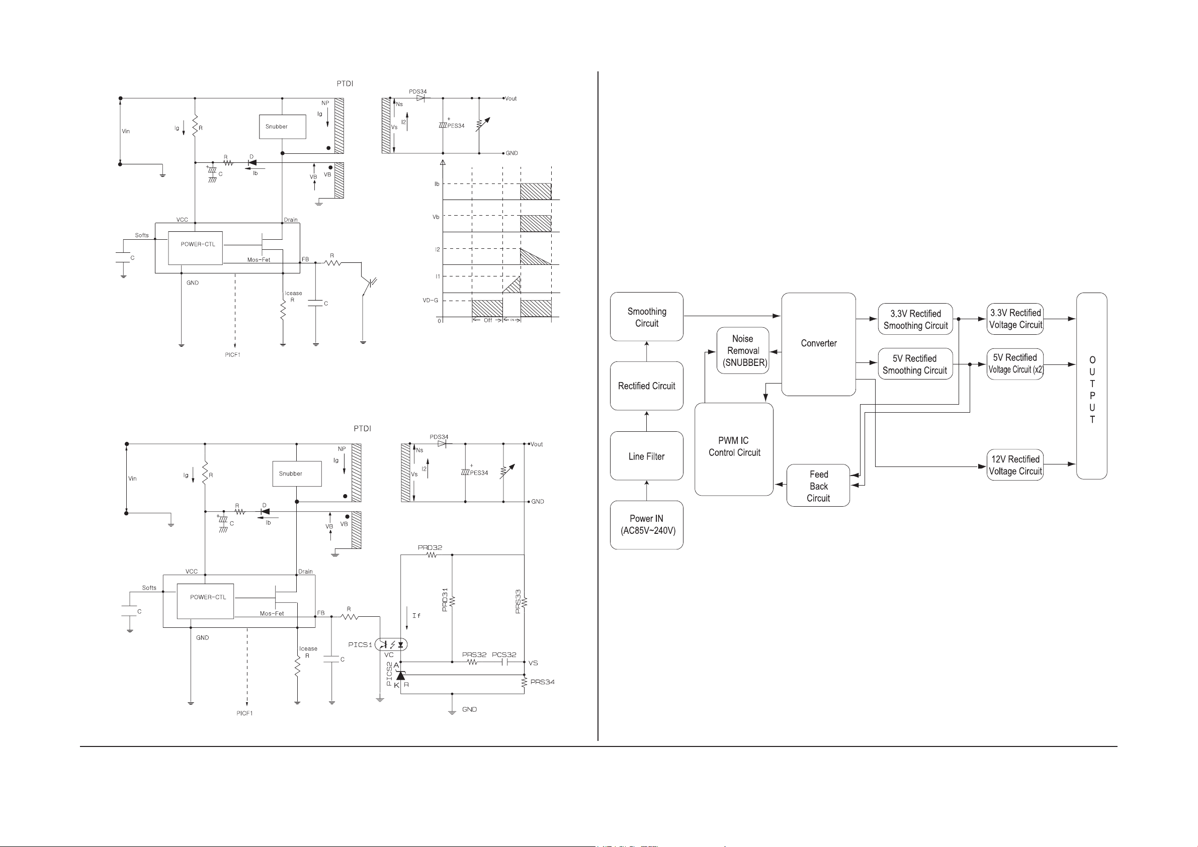
u Operation descriptions
1) Internal OP-Amp '+' base potential of PICS2 is 2.5V and external "-" input potential is
connected with PRS33 and PRS34 to maintain Vout of 4.4V.
2) If load of 4.4V terminal increase (or AC inout voltage decrease) and Vout decrease over 4.4V,
Then : PICS2 "R" potential decrease over 2.5V --> PICS2 A-K BASE Current decrease -->
PICS2 A-K Current decrease --> PICS1 DIODE Current decrease --> PICS1 C-E Current decrease -->
PICS1 C-E Voltage increase -
-> PICS1 F-B Voltage increase --> OUT DUTY increase TRANS Primary Cuttent Increase -->
TRANS Primary Power increase --> Vout increase --> Vout maintain 4.4V
- PRD31, PRD32 : Reduce 4.4V overshoot.
- PRS32, PCS32 : Prevent PICS2 oscillation (for phase correction).
7-2-3 Internal Block Diagram
u Internal Block Diagram
(d) Feedback Control Circuit
Fig. 7-3 Driving Circuit
Fig. 7-5
Fig. 7-4
7-4 This Document can not be used without Samsung's authorization Samsung Electronics
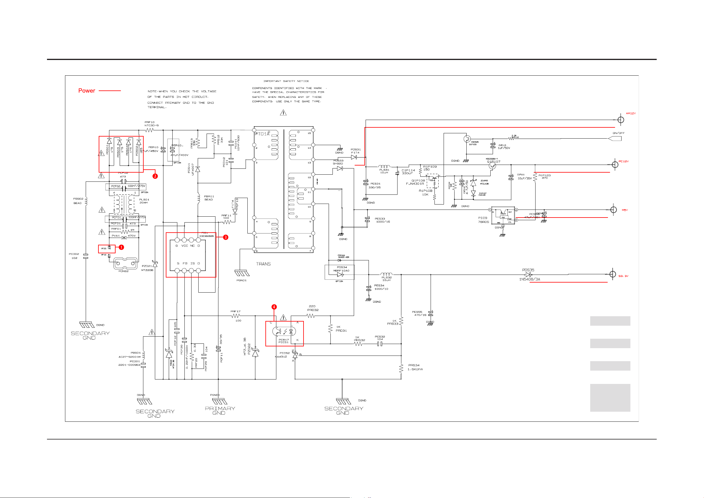
7-3 S.M.P.S (S.M.P.S PCB)
Schematic Diagrams
q PF2S
DC 180V
w PDS01~04
DC 110-350V
e PIC1
AC 100-240V
r PICS1
1. (8.3V)
2. (2.5V)
3. (1.8V)
4. (1.9V)
Samsung Electronics This Document can not be used without Samsung's authorization 7-5
 Loading...