


2
CC OO NN TT EE NN TT SS
ⅠⅠ.. SSPPEECCIIFFIICCAATTIIOONN
1. CAMERA SPECIFICATION ……………………………………………………………………………………… 4
2. SYSTEM REQUIREMENTS ……………………………………………………………………………………… 5
3. TFT LCD PANEL MARK ………………………………………………………………………………………… 6
4. CONNECTION DIAGRAM ………………………………………………………………………………………… 8
5. IDENTIFICATION OF FEATURES………………………………………………………………………………… 9
ⅡⅡ.. IINNSSTTAALLLLAATTIIOONN
…………………………………………………………………………………………… 11
ⅢⅢ.. EEXXPPLLOODDEEDD VVIIEEWW AANNDD PPAARRTTSS LLIISSTT
1. MAIN ASSEMBLY…………………………………………………………………………………………………16
2. BODY COVER ASSEMBLY ………………………………………………………………………………………18
3. FRONT COVER ASSEMBLY …………………………………………………………………………………… 20
4. BACK COVER ASSEMBLY ………………………………………………………………………………………22
5. PACKING ITEM……………………………………………………………………………………………………24
ⅣⅣ.. AADDJJUUSSTTMMEENNTT
1. DIGITAL CAMERA SERVICE ……………………………………………………………………………………27
2. How to check the FIRMWARE VERSION………………………………………………………………………33
3. How to update the FIRMWARE UPGRADE ……………………………………………………………………34
4. ADJUSTMENT ……………………………………………………………………………………………………36
ⅤⅤ.. PPAATTTTEERRNN DDIIAAGGRRAAMM
1. PARTS ARRANGEMENT FOR EACH PCB ASS’Y
1) MAIN_TOP…………………………………………………………………………………………………44
2) MAIN_BOTTOM……………………………………………………………………………………………45
3) KEY_TOP …………………………………………………………………………………………………46
4) KEY_BOTTOM ……………………………………………………………………………………………47
5) USB_TOP …………………………………………………………………………………………………48
6) USB_BOTTOM ……………………………………………………………………………………………49
7) FLASH_TOP ………………………………………………………………………………………………50
8) FLASH_BOTTOM …………………………………………………………………………………………51
ⅥⅥ.. CCIIRRCCUUIITT DDIIAAGGRRAAMM
1. BLOCK DIAGRAM…………………………………………………………………………………………………52
2. CIRCUIT DIAGRAM
1) CCD_MN39482 ……………………………………………………………………………………………53
2) SPCA536 DSP………………………………………………………………………………………………54
3) IMAGE PERIPHERIC ………………………………………………………………………………………55
4) SDRAM_TRAP_EEPROM ………………………………………………………………………………56
5) FLASHROM-NandFlash-SD ………………………………………………………………………………57
6) USB1.1_MIC_TVOUT_BUZZE …………………………………………………………………………58
7) INTERFACE IO ……………………………………………………………………………………………59
8) POWER_MAX1567…………………………………………………………………………………………60
9) CASIO 1.8 inch 3G Panel ………………………………………………………………………………61
10) D402 LENS_USB ………………………………………………………………………………………62
11) D402Shutter_Strobe ……………………………………………………………………………………63

3
ⅦⅦ.. TTRROOUUBBLLEESSHHOOOOTTIINNGG
1. CHECK LIST FOR REPAIRING …………………………………………………………………………………64
2. MAIM TROUBLESHOOTING………………………………………………………………………………………65
3. HOW TO ASSEMBLY ……………………………………………………………………………………………76
ⅧⅧ.. SSEERRVVIICCEE IINNFFOORRMMAATTIIOONN
…………………………………………………………………………………80

Type 1/2.5" CCD
Effective Pixels Approx. 4.0 Mega-pixel
Total Pixels Approx. 4.2 Mega-pixel
Lens f=5.8mm
(35mm film equivalent:35mm)
F No. F 3.5 / F7.0
Still Image mode: 1.0X ~ 4.0X
Play mode: 1.0X ~ 7.0X (depends on Image size)
LCD 1.8" color TFT LCD
Type Fixed focus with two steps manual adjustment
Macro: 0.2m
Normal: 1.0m~infinity
Type Mechanical and Electronic shutter
Speed 2 - 1/1000 sec.(8 – 1/1000sec.in Night Mode)
Programmed AE
Metering: Multi, Spot
Compensation ±2.0EV (0.5EV steps)
ISO Equivalent Auto,100,200,400
Modes Auto, Auto & Red - eye reduction, Fill-in flash, Slow sync, Flash Off
Range 0.2m ~ 2.5m
Recharging Time Approx. 5 sec.
Sharpness Soft, Normal, Vivid
Effect Normal, B&W, Sepia
White Balance Auto, Daylight, Cloudy, Sunset, Fluorescent(H), Fluorescent(L), Tungsten, Custom
Photo Frame 9 Frames
Voice Recording (max. 1 hour)
Voice Memo on Still Image (max. 10.sec)
Date Imprinting Off, Date, Date & Time (User selectable)
Mode: Auto, Program, Scene
Scene : Night, Portrait, Landscape, Fireworks
Shooting: Single, continuous
With audio (recording time: memory capacity dependent)
Size: 640 x 480, 320 x 240 Frame rate: 24, 15fps
Self-timer 2sec, 10 sec, Double self (10/2sec.)
Internal memory: 16MB flash memory
External memory: SD card /MMC
(Up to 512MB Guaranteed)
Still Image: JPEG (DCF), EXIF 2.2, DPOF 1.1, PictBridge 1.0
Movie Clip: AVI (MJPEG) Audio: WAV
4
ⅠⅠ.. SSPPEECCIIFFIICCAATTIIOONN
Image Sensor
Lens
Focal Length
Range
Control
Digital Zoom
Focusing
Shutter
Exposure
Flash
Voice Recording
Shooting
Storage
Movie Clip
Still Image
Media
File Format
1. CAMERA SPECIFICATION
2272 : 2272X1704 2048 : 2048X1536
Image Size 1600 : 1600X1200 1024 : 1024X768
640 : 640X480
2272 : Super fine (10) Fine (20) Normal (33)
2048 : Super fine (13) Fine (27) Normal (42)
1600 : Super fine (17) Fine (37) Normal (50)
1024 : Super fine (38) Fine (78) Normal (113)
640 : Super fine (81) Fine (145) Normal (234)
* These figures are measured under Samsung’s standard conditions and may
vary depending on shooting conditions and camera settings.
Type Single image / Thumbnails / Slide show/ Movie clip
Editing Rotation, Trimming, Resizing
Interface Digital output connector: USB 1.1
Primary battery : 2 x AA alkaline, Lithium, Ni-Mn,
Ni-Zn, 1X CR-V3
Rechargeable battery : 2 x AA Ni-MH,
Ni-Cd / 1 x I-Pack (SBP-1303)
Dimensions (WxHxD) 96.5 x 52.5 x 30.5 mm
Weight Approx. 90g (without batteries and card)
Operating Temperature 0 ~40 °C
Operating Humidity 5 ~85%
Storage Driver (Windows98/98SE)
Digimax Viewer, Arcsoft PhotoImpression
5
ⅠⅠ.. SSPPEECCIIFFIICCAATTIIOONN
Capacity
(16MB)
Storage
Image Play
Power Source
Software
Camera Driver
Application
For Windows For Macintosh
PC with processor better than MMX Power Mac G3 or later
Pentium 233MHz (XP : Pentium II 300MHz)
Windows 98/98SE/2000/ME/XP Mac OS 9.2~10.3
Minimum 32MB RAM (XP : 128MB) Minimum 64MB RAM
140MB of available hard-disk space 110MB of available hard-disk space
USB port USB port
CD-ROM drive CD-ROM drive
800x600 pixels, 16-bit colour display QuickTime 6.01 or later for Movie Clip
compatible monitor (24-bit colour display
recommended)
2. SYSTEM REQUIREMENTS
■ Recording Mode
6
ⅠⅠ.. SSPPEECCIIFFIICCAATTIIOONN
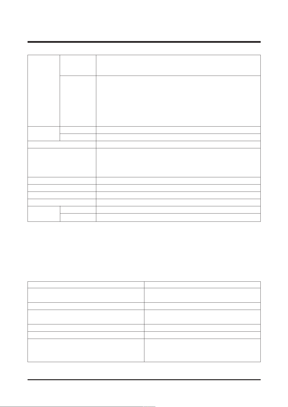
No. Description Icons
1 Battery
3 Continuous shot
4 Flash
5 Self-timer
6 Macro
7 Metering
8 Card inserted indicator
9 Camera shake warning
10 Date/Time 2005/03/01 00:00AM
11 Exposure compensation
12 White Balance
13 ISO
14 Sharpness
15 Image qualty
16 Image size 2272, 2048, 1600, 1024, 640
Number of available shots remaining 20
Remaining time(Movie clip/Voice recording) 00:01:11/ 00:25:50
18 Voice memo
19 Digital Zoom rate
17
②
③
④
⑤
⑥
⑦
⑧
⑪
⑫
⑬
⑭
⑮
⒃
⒔
⑩
⑨
⒖
⒕
①
Recording mode
2
3. TFT LCD PANEL MARK
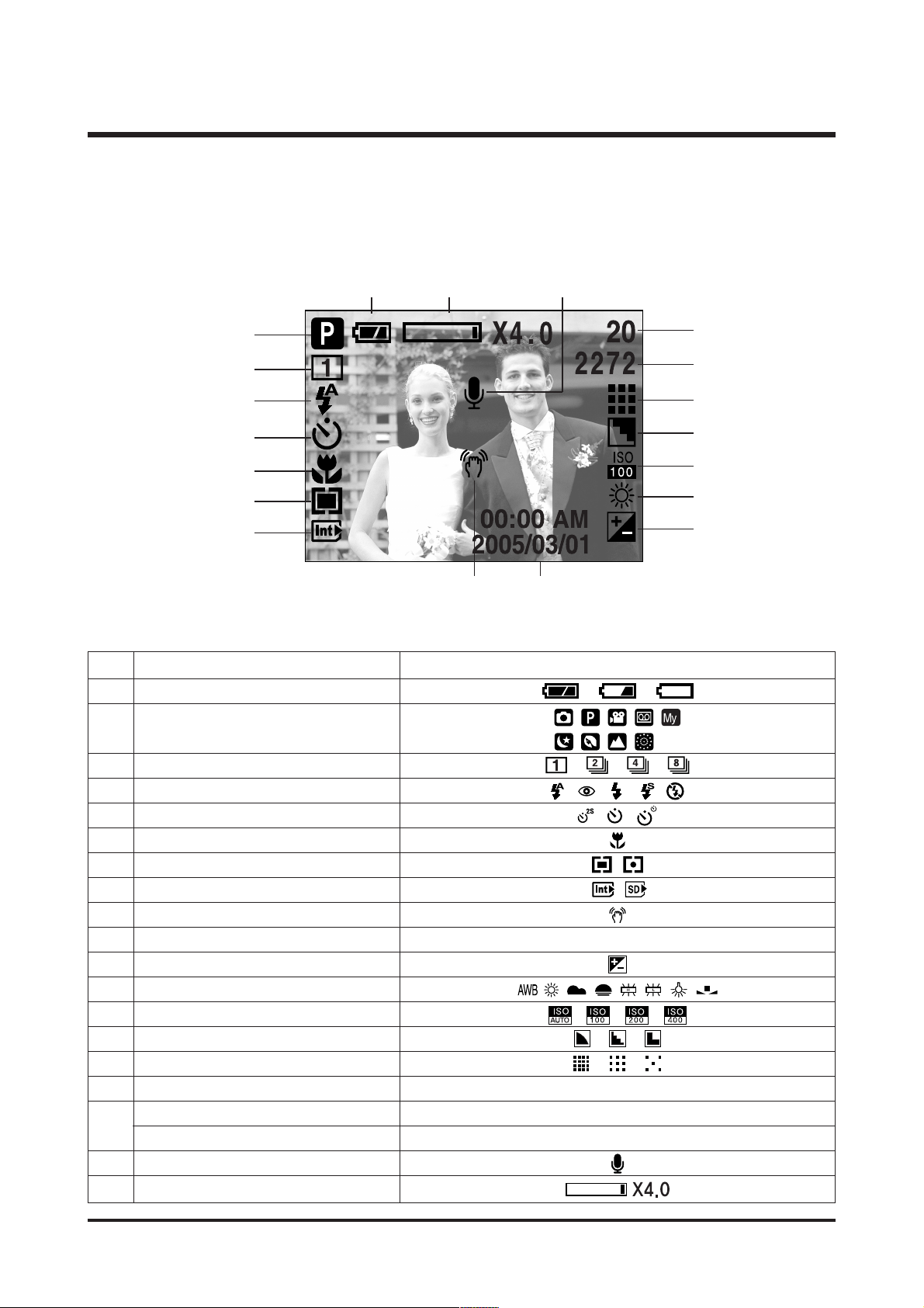
■ Play Mode
NO. Description Icons
1 Battery
2 Play mode
3 File Type
4 Voice memo
5 Protect indicator
6 DPOF indicator
7 Stored image number 100-0009
7
ⅠⅠ.. SSPPEECCIIFFIICCAATTIIOONN
100-0009
①
⑦
②
③
④
⑤
⑥
SIZE : 2272X1704 Size
AV : F3.5 Aperture value
TV : 1/18 Shutter speed
FLASH : OFF Whether or not the
flash is used.
DATE : 2005/03/01 Recording date
100-0009
SIZE : 2272X1704
AV : F3.5
TV : 1/18
FLASH : OFF
DATE : 2005/03/01
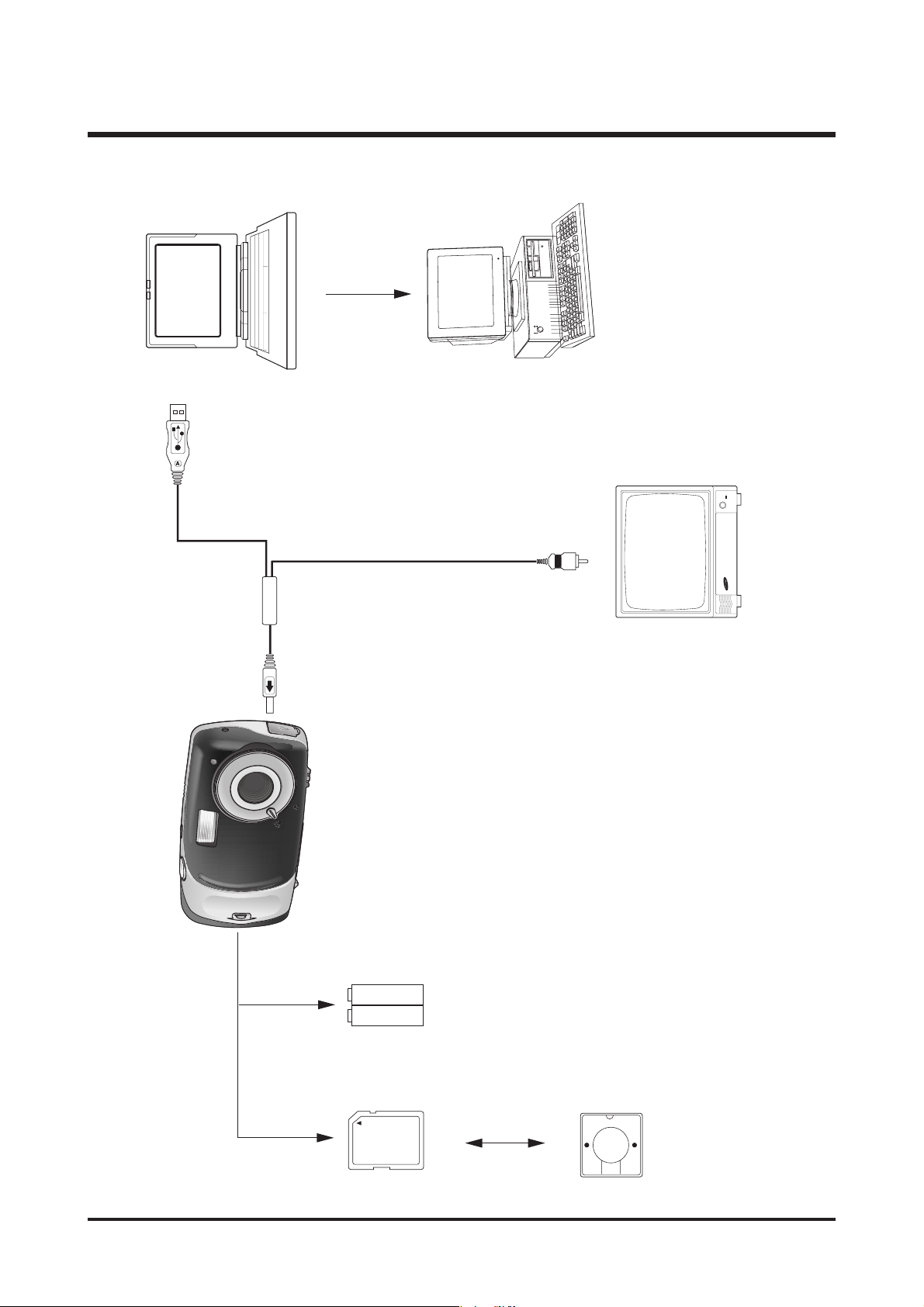
4. Connection Diagram
8
ⅠⅠ.. SSPPEECCIIFFIICCAATTIIOONN
USB Cable
Lap top
IBM / MAC
Video Cable
TV Monitor
SNB-2312
SD Card
Card Reader

9
ⅠⅠ.. SSPPEECCIIFFIICCAATTIIOONN
Tripod socket
Focus ring
Flash
Strap eyelet
LCD monitor
Shutter button
Mode button
Power button
Play mode button
Microphone
Self-timer lamp
Lens
5-function button
LCD button
Zoom T button
(Digital zoom)
Camera status lamp
USB
connection port
+/-, DELETE button
Zoom W button
(Thumbnail)
5. Identification of Features
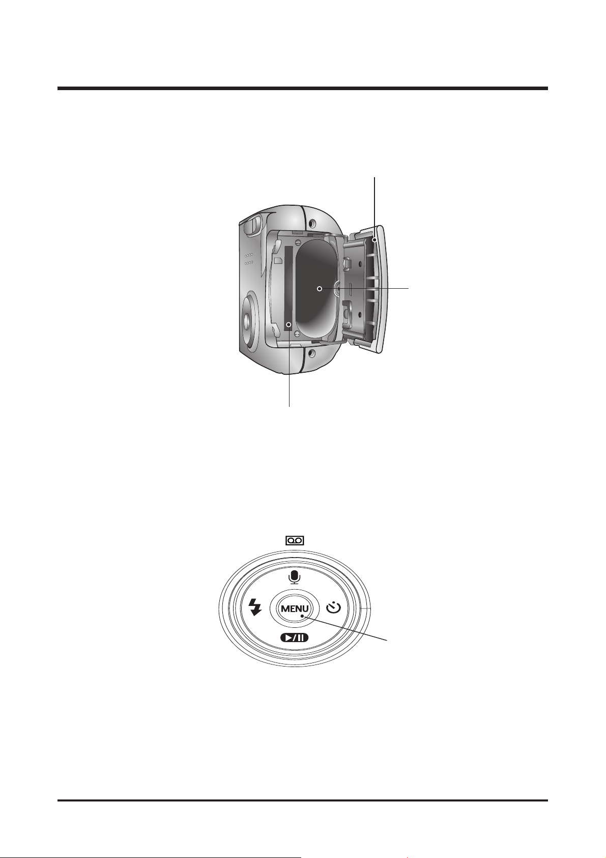
10
ⅠⅠ.. SSPPEECCIIFFIICCAATTIIOONN
FLASH/ LEFT
button
MENU/
OK button
PLAY&PAUSE/ DOWN button
SELF-TIMER/
RIGHT button
Voice Recording/
Voice memo/ UP button
Memory card slot
Battery chamber
Battery chamber cover
※ The OK button written in this manual means the MENU button.
11
ⅡⅡ.. IINNSSTTAALLLLAATTIIOONN
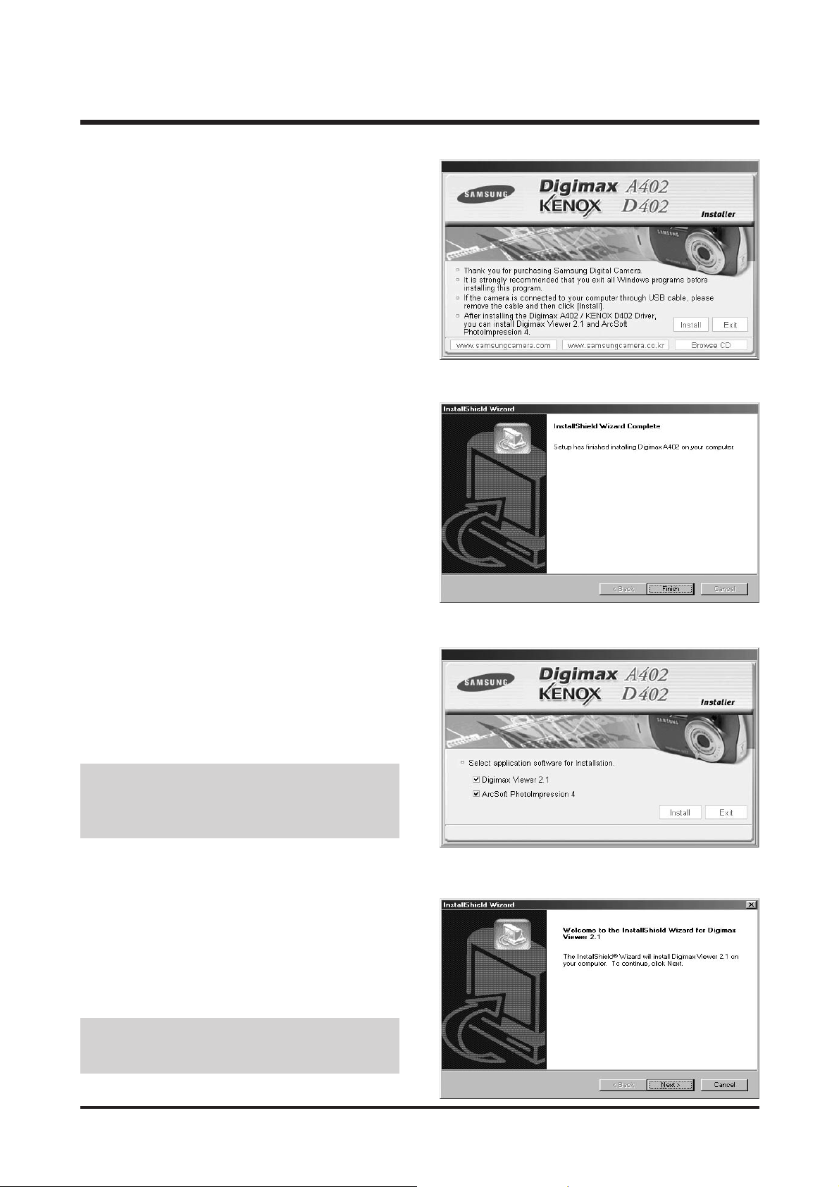
1. Click the [Install] menu in the Autorun frame.
The camera driver is installed automatically.
2. Camera driver installation is complete.
Click the [Finish] button.
3. A window for which you can select application
software will be displayed. Select the application
program and click the [Install] button. Refer to page
88 for more information about the application
program.
4. Install Digimax Viewer.
Click [Next >] button.
● If you select [Exit] at the step 3, the
application program installation will be
cancelled.
● If you select [Cancel] at step 4, a window for
installing PhotoImpression will be displayed.

12
ⅡⅡ.. IINNSSTTAALLLLAATTIIOONN
8. Digimax Viewer installation is successfully
completed. Click the [Finish] button to install
PhotoImpression. The system will not reboot even if
the [Yes, I want to restart the computer now] option
is selected.
* The frame 8 may not appear according to the
system requirements.
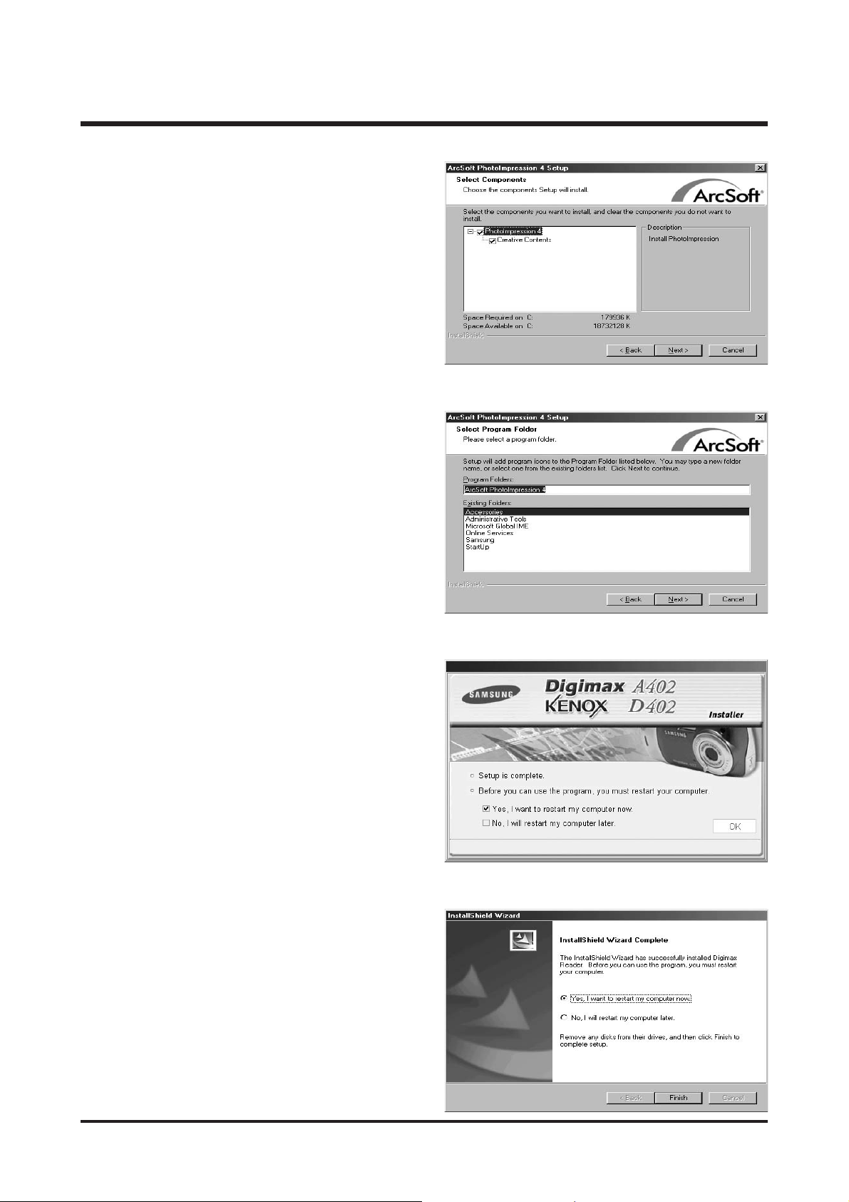
7. A window will open, asking you to choose a folder
to which program icons will be added.
Click [Next >] button. If you want to add the
program icons to a different folder, choose another
folder, and then click [Next >] button.
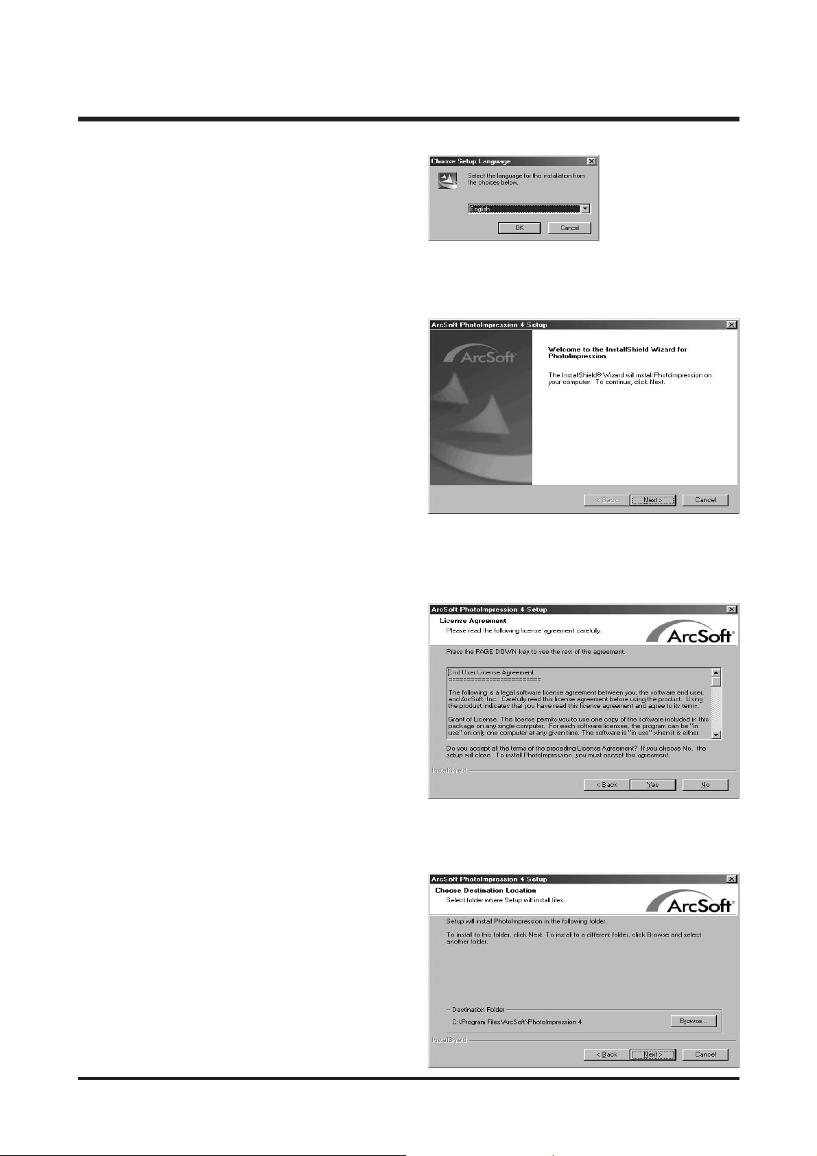
5. The Software License Agreement window will be
displayed. If you agree to this, click [Yes], the
window will then move to the next step.
If you disagree, click [No] and the installation
program will be cancelled.
6. A destination selection window will open.
Click [Next >]. To copy to the files to another folder,
click [Browse...] and choose a folder you want.
13
ⅡⅡ.. IINNSSTTAALLLLAATTIIOONN
9. The PhotoImpression installation window will be
displayed as shown alongside.
Click the [OK] button.
10. A Welcome window will be displayed.
Click the [Next >] button.
12. A destination selection window will open.
Click [Next >]. To copy to the files to another
folder, click [Browse...] and choose a folder you
want.
11. The Software License Agreement window will be
displayed. If you agree to this, click [Yes], the
window will then move to the next step.
If you disagree, click [No] and the installation
program will be cancelled.
14
ⅡⅡ.. IINNSSTTAALLLLAATTIIOONN
15. Installation is complete. To apply changes, you
must restart the computer.
Select [Yes, I want to restart my computer now],
and then click [OK].
* The frame 15 may be displayed according to the
system requirements.
Click the [Finish] button to restart the computer.
13. The [Select Components] window will appear.
Click [Next >] button.
14. A window will open, asking you to choose a folder
to which program icons will be added.
Click [Next >] button. If you want to add the
program icons to a different folder, choose another
folder, and then click [Next >] button.

15
ⅡⅡ.. IINNSSTTAALLLLAATTIIOONN
16. After restarting the computer, connect the PC to the camera with the USB cable.
17. Turn the camera power on. [Found New
Hardware Wizard] will open and the computer will
recognise the camera.
* If you have ever installed an image viewer
program or your OS is Windows XP, an image
viewer program will open. If the image viewer
program opens, the camera driver was setup
successfully.
18. If you can see [Removable Disk] under [My
computer], the camera driver installation was
successful. Now you can transfer image files from
the camera to PC via the USB cable.
● If you have installed the camera driver, [Found New Hardware Wizard] may not open.
● On a Windows 98 or 98 SE system, the Found New Hardware Wizard dialog box opens and a window asking
you to select a driver file may appear. In this case, specify "USB Driver" in the CD supplied.
● Before connecting the camera to the PC, You should first install the camera driver.
● After installing the camera driver, you have to restart your PC.
● If you connect the camera to the PC before installing the camera driver, the [Found New Hardware Wizard] will
open.
In this case, cancel the [Found New Hardware Wizard] and disconnect the camera. Install the camera driver and
connect the camera to the PC again.
● Should the computer not find the camera driver after installation, please try one or more of the following
measures.
1. Delete the camera driver , and re-install the driver.
2. Refer to FAQ to check for a possible solution to the problem.
3. If your PC’s central processing unit is VIA chip (This is shown in the USB Host Controller), download the patch
file from the Samsung Camera web page. (http://www.samsungcamera.com)

16
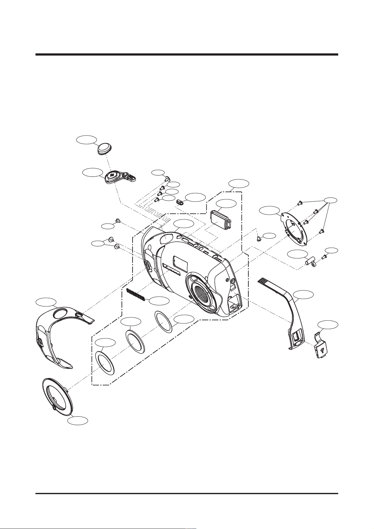
ⅢⅢ.. EEXXPPLLOODDEEDD VVIIEEWW AANNDD PPAARRTT LLIISSTT
1. MAIN ASSEMBLY
1-7
1-2
1-4
1-1
3
1-
1-6
1-5
1-3

17
ⅢⅢ.. EEXXPPLLOODDEEDD VVIIEEWW AANNDD PPAARRTT LLIISSTT
▶▶
PARTS LIST
1-1 Q9007230001A Front Cover Asscmbly-Blue(KENOX D402) 1
Q9007230701A Front Cover Asscmbly-Silver(KENOX D402) 1
Q9007230801A Front Cover Asscmbly-Red(KENOX D402) 1
Q9007231101A Front Cover Asscmbly-Blue(DIGIMAX A402) 1
Q9007231201A Front Cover Asscmbly-Silver(DIGIMAX A402) 1
Q9007231301A Front Cover Asscmbly-Red(DIGIMAX A402) 1
1-2 Q9007230101A Back Cover Asscmbly-Blue 1
Q9007230901A Back Cover Asscmbly-Silver 1
Q9007231001A Back Cover Asscmbly-Red 1
1-3 Q6009002901A Screw 4
1-4 Q6003045901A Screw 2
1-5 Q6009003001A Screw 2
1-6 Q6009003101A Screw 2
1-7 Q6009003201A Screw 1
Fig.No Parts No. Parts Name Q’ty Remarks

18
ⅢⅢ.. EEXXPPLLOODDEEDD VVIIEEWW AANNDD PPAARRTT LLIISSTT
2. BODY ASSEMBLY
2-26
2-15
2-11
2-12
2-3
2-4
2-2
2-1
2-2
2-1
2-17
2-24
2-7
2-16
2-18
2-20
2-23
2-24
2-25
2-30
2-28
2-29
2-19
2-13
2-5
2-6
2-8
2-10
2-9
2-14
2-21
2-24
2-22
2-27

19
ⅢⅢ.. EEXXPPLLOODDEEDD VVIIEEWW AANNDD PPAARRTT LLIISSTT
▶▶
PARTS LIST
2-1 Q7009000301A Battery Stop Axle 1
2-2 Q7009000101A Battery Cover Axle 1
2-3 Q6107064801A Battery Spring Washer 1
2-4 Q6107064901A Battery Cover Spring 1
2-5 Q7009000201A Trigger Contact 1
2-6 Q7309044801A Flash Rubber 1
2-7 Q7204023101A Battery Compartmant 1
2-8 Q0611004101A Flash Tube 1
2-9 Q2401009101A Photo Flash CAP 1
2-10 Q3002001401A Piezo Buzzer 1
2-11 Q7001004901A Battery Contact Lower 1
2-12 Q7209001401A Battery Stopper 1
2-13 Q0607000901A Flash Retlector 1
2-14 Q7101000601A Battery Contact Upper 2
2-15 Q7217356701A Ass'y Battery Cover-Blue 1
Q7204023301A Ass'y Battery Cover-Silver 1
Q7204023401A Ass'y Battery Cover-Red 1
2-16 Q9008086401A Ass'y Shutter 1
2-17 Q7309044501A MIC Rub Contact 1
2-18 Q7204023201A PCB FIX BOSS 1
2-19 Q9002140101A Lens Assembly 1
2-20 Q9001103201A Battery Compartmant Assmbly 1
2-21 Q7001005001A Tube Contact 1
2-22 Q9008086501A Ass'y USB 1
2-23 Q9008086601A Ass'y Main 1
2-24 Q6003042301A Screw 6
2-25 Q6003039401A Screw 3
2-26 Q7409190801A Flash Mylar 1
2-27 Q7409190901A USB Mylar 1
2-28 Q7309046501A CCD Rubber 1
2-29 Q0604005201A CCD Sensor 1
2-30 Q7101000701A CCD Plate 1
Fig.No Parts No. Parts Name Q’ty Remarks
20
ⅢⅢ.. EEXXPPLLOODDEEDD VVIIEEWW AANNDD PPAARRTT LLIISSTT
3. FRONT COVER ASSEMBLY
3-8
3-5
3-7
3-19
3-16
3-2
3-3
3-17
3-6
3-16
3-16
3-16
3-10
3-4
3-9
3-15
3-20
3-14
3-16
3-13
3-12
3-16
3-18
3-11
3-1

21
ⅢⅢ.. EEXXPPLLOODDEEDD VVIIEEWW AANNDD PPAARRTT LLIISSTT
3-1 Q7204022801A Focus Ring 1
3-2 Q7409190401A Lens Panel 1
3-3 Q7209000601A Lens Cover 1
3-4 Q7409190501A Lens Plate Tape 1
3-5 Q7217356301A Ass'y Middle Cover 1
3-6 Q7217303501A Samsung Plate 1
3-7 Q7204022901A Power Release Button Arm 1
3-8 Q7209000701A Ass'y Release Button 1
3-9 Q7209000801A Ass'y Power Button 1
3-10 Q7217356401A Front Cover-Blue(KENOX D402) 1
Q7217357101A Front Cover-Silver(KENOX D402) 1
Q7217357201A Front Cover-Red(KENOX D402) 1
Q7217357301A Front Cover-Blue(DIGIMAX A402) 1
Q7217357401A Front Cover-Silver(DIGIMAX A402) 1
Q7217357501A Front Cover-Red(DIGIMAX A402) 1
3-11 Q7309046301A USB Cover TPU 1
3-12 Q7217356501A Ass'y Middle Cover-2 1
3-13 Q7209000901A Front Led Guide 1
3-14 Q7101000501A Lens Cover Sheet Metal 1
3-15 Q7217356601A Flash Cover 1
3-16 Q6003031501A Screw 11
3-17 Q6009003301A Screw 1
3-18 Q6003045901A Screw 1
3-19 Q6003031301A Screw 2
3-20 Q9007231401A Front Cover SUB Asscmbly-Blue(KENOX D402) 1
Q9007231501A Front Cover SUB Asscmbly-Silver(KENOX D402) 1
Q9007231601A Front Cover SUB Asscmbly-Red(KENOX D402) 1
Q9007231701A Front Cover SUB Asscmbly-Blue(DIGIMAX A402) 1
Q9007231801A Front Cover SUB Asscmbly-Silver(DIGIMAX A402) 1
Q9007231901A Front Cover SUB Asscmbly-Red(DIGIMAX A402) 1
Fig.No Parts No. Parts Name Q’ty Remarks
▶▶
PARTS LIST

22
ⅢⅢ.. EEXXPPLLOODDEEDD VVIIEEWW AANNDD PPAARRTT LLIISSTT
4. BACK COVER ASSEMBLY
4-12
4-1
4-11
4-10
4-5
4-13
4-2
4-3
4-14
4-4
4-6
4-9
4-8
4-7
4-15

23
ⅢⅢ.. EEXXPPLLOODDEEDD VVIIEEWW AANNDD PPAARRTT LLIISSTT
4-1 Q9007232001A Back Cover SUB Assnbly-Blue 1
Q9007232101A Back Cover SUB Assnbly-Silver 1
Q9007232201A Back Cover SUB Assnbly-Red 1
4-2 Q9008086301A Key Assembly 1
4-3 Q7309046401A Key Pad Rubber 1
4-4 Q7209001001A Ass'y OK Button 1
4-5 Q7209001101A Ass'y Direction Button 1
4-6 Q7204023001A Ass'y Button 1
4-7 Q7001004801A TFT Holder 1
4-8 Q0704011501A TFT LCD 1
4-9 Q7409190601A TFT Sponge 1
4-10 Q7217356801A Back Cover-Blue 1
Q7217356901A Back Cover-Silver 1
Q7217357001A Back Cover-Red 1
4-11 Q7209001201A Led Guide Back 1
4-12 Q7209001301A Ass'y Zomm Button 1
4-13 Q6003031501A Screw 4
4-14 Q6009003401A Screw 5
4-15 Q7409190701A TFT Mylar 1
Fig.No Parts No. Parts Name Q’ty Remarks
▶▶
PARTS LIST
24
ⅢⅢ.. EEXXPPLLOODDEEDD VVIIEEWW AANNDD PPAARRTT LLIISSTT
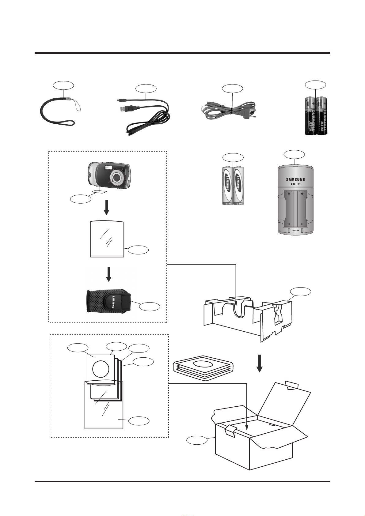
5. PACKING ITEM
5-10
5-13
5-11 5-14
5-1
5-15
5-9
5-16
5-12
5-5
5-3
5-4
5-6
5-7
5-2
5-8

25
ⅢⅢ.. EEXXPPLLOODDEEDD VVIIEEWW AANNDD PPAARRTT LLIISSTT
5-1 QP960210101A PE BAG (FOR CAMERA) 1
5-2 Q6909011601A PE BAG (FOR ACCESSORY) 1
5-3 Q6901208301A INNER PAD_D Digimax A402_KOR/EXP 1
5-4 Q6904026401A POUCH_Digimax A402 (SAMSUNG) 1
5-5 Q6806254401A Q/GUIDE_KENOX D402_KOR 1
Q6806254501A Q/GUIDE_Digimax A402_ENG 1
Q6806254601A Q/GUIDE_Digimax A402_GER 1
Q6806254701A Q/GUIDE_Digimax A402_FRA 1
Q6806254801A Q/GUIDE_Digimax A402_SPA 1
Q6806254901A Q/GUIDE_Digimax A402_ITA 1
Q6806255001A Q/GUIDE_Digimax A402_TUR 1
Q6806255101A Q/GUIDE_Digimax A402_DUT 1
Q6806255201A Q/GUIDE_Digimax A402_POR 1
Q6806255301A Q/GUIDE_Digimax A402_SWE 1
Q6806255401A Q/GUIDE_Digimax A402_DEN 1
Q6806255501A Q/GUIDE_Digimax A402_FIN 1
Q6806255601A Q/GUIDE_Digimax A402_RUS 1
Q6806255701A Q/GUIDE_Digimax A402_CHI(S) 1
Q6806255801A Q/GUIDE_Digimax A402_CHI(T) 1
5-6 Q6806255901A U/MANUAL_KENOX D402_KOR 1
Q6806256001A U/MANUAL_Digimax A402_ENG 1
Q6806256101A U/MANUAL_Digimax A402_GER 1
Q6806256201A U/MANUAL_Digimax A402_FRA 1
Q6806256301A U/MANUAL_Digimax A402_SPA 1
Q6806256401A U/MANUAL_Digimax A402_ITA 1
Q6806256501A U/MANUAL_Digimax A402_TUR 1
Q6806256601A U/MANUAL_Digimax A402_DUT 1
Q6806256701A U/MANUAL_Digimax A402_POR 1
Q6806256801A U/MANUAL_Digimax A402_SWE 1
Q6806256901A U/MANUAL_Digimax A402_DEN 1
Q6806257001A U/MANUAL_Digimax A402_FIN 1
Q6806257101A U/MANUAL_Digimax A402_RUS 1
Q6806257201A U/MANUAL_Digimax A402_CHI(S) 1
Q6806257301A U/MANUAL_Digimax A402_CHI(T) 1
5-7 Q6807002601F WARRANTY CARD_KOREA 1
Q6807003003U WARRANTY CARD_EXP 1
Q6807010903C WARRANTY CARD_RUS(3 YEARS) 1
Q6807011301B WARRANTY CARD_TSOE(CHINA) 1
5-8 Q6901208401A G/T BOX_KENOX D402_KOR 1
Q6901208501A G/T BOX_Digimax A402_EXP/AUS 1
Q6901208601A G/T BOX_Digimax A402_USA/CAN 1
5-9 Q4301001801A "ALKALINE (1.5V, AA) 2EA - DURACEL ULTRA" 1
Fig.No Parts No. Parts Name Q’ty Remarks
▶▶
PARTS LIST

26
ⅢⅢ.. EEXXPPLLOODDEEDD VVIIEEWW AANNDD PPAARRTT LLIISSTT
5-10 Q7409121701A STRAP_D301/D202/D401/U-CA 501/D402_KOR/EXP 1
5-11 Q3801002801A USB CABLE_D200/201/300/301/202 1
5-12 Q4609011001A
DRIVER + Digimax Viewer 2.1+ Arcsoft PhotoImpression 4.0
1
5-13 Q7409185401A FCC LABEL_Digimax A402_EXP (MADE IN CHINA) 1
Q7409185501A FCC LABEL_Digimax A402_EXP (MADE BY SAMSUNG) 1
5-14 Q3801003001A AC CODE CABLE_KOR-D1 1
Q3801003201A AC CODE CABLE_EXP-D1 1
Q3801003101A AC CODE CABLE_USA-D1 1
Q3801001001A AC CODE CABLE_UK-DSC220SE 1
Q3801003401B AC CODE CABLE_AUS-D1 1
5-15 Q4301003101A "Ni-MH BATTERY SNB-2312 (1.2V, AA) - SAMSUNG" 1
5-16 Q4301003001A Ni-MH CHARGER SBC-N1 1
Fig.No Parts No. Parts Name Q’ty Remarks
27
ⅣⅣ.. AADDJJUUSSTTMMEENNTT
To take a digital camera service(Repair, Tuning and Checking), the following equipments have to be
arranged.
The sequences for the camera service are as shown
alongside.
1. Receiving the camera
When receiving a camera, check whether the accessories
are included or not and ask the customer exact problems.
2. Checking the camera
Checking the camera with priority given to the exact
problems to find overall malfunctions.
3. Repairing the camera
Repair the camera malfunctions found at the step 2.
4. Inspection
After repairing the camera, inspect all of the camera
functions.
1. Digital camera service
※ The illustrations may be different from the real display in accordance with the camera model.
1. Checking the camera and
Inspection
2. Repairing the camera 3. Tuning
Receiving the camera
Checking the camera
Repairing the camera
Tuning
Inspection
Finish

28
ⅣⅣ.. AADDJJUUSSTTMMEENNTT
1) Equipments for checking and inspection
To check and inspect the camera malfunction, the following equipments have to be arranged.
①①
②②
③③
⑤⑤
⑥⑥
⑦⑦
⑧⑧
⑪⑪
⑨⑨
⑩⑩
④④
No. Device Description
1 PC for inspection - Installing a digital camera driver or Checking the removable device
- Checking the file transference(upload and download)
- Playing back the still image or movie clip
2 HARD RACK, For the compatibility test.
by Operating System by the O/S(WIN 98SE, ME, 2000, XP)
3 Driver CD, by camera models S/W CDs for installing a camera driver
4 USB HUB For using all kinds of USB cable at a time
5 USB cable, by camera models For checking file transference(upload and download) by camera models
6 Chart for checking colors For checking color and image resolution before or after camera repair
7 TV MONITOR For checking video output and whether NTSC/PAL can be selected
8 Memory card by types For checking card recognition by brands and sizes
9 A/V CABLE For checking whether the image can be displayed on a external monitor
10 POWER SUPPLY For checking camera power by camera models
11 Power cable by camera models

29
ⅣⅣ.. AADDJJUUSSTTMMEENNTT
2) Equipments for camera repair
To repair the camera, the following equipments have to be arranged.
①①
②②
③③
⑤⑤
⑥⑥
⑪⑪
⑨⑨
④④
⑩⑩
⑧⑧
⑪⑪
⑫⑫
⑬⑬
⑦⑦
No. Device Description
1 A set of tools Pincette/ Screwdriver/ Discharger etc.
2 Cleaning paper For cleaning camera lens and camera parts
3 Detergent container For containing detergent
4 Parts case For keeping various camera parts and disassembled camera parts
5 Anti-electricity mat For repairing table made from anti-electricity material
6 Soldering sponge For removing solder
7 Air pump For removing various kinds of dust
8 LIGHT BOX Color temperature 5100
9 POWER SUPPLY 7.5V 2.0A
10 Soldering iron Soldering iron that can select temperature
11 Tester Portable tester that can test AC/DC, Ω,♪ ect.
12 BATTERY & AC ADAPTOR & Rechargeable battery by camera models
AC ADAPTOR - SBP3603/ SBP3605/ SBP3606
- SLB 1437
- SBP 1103

30
ⅣⅣ.. AADDJJUUSSTTMMEENNTT
3) Equipments for camera tuning
To tune the camera, the following equipments have to be arranged.
①①
②②
③③
⑤⑤
⑥⑥
④④
No. Device Description
1 AE TESTER For tuning AE and STROBE
2 AWB LIGHT For checking and tuning AWB
SOURCE BOX
3 COLOR chart For checking AWB and color of images
4 AF chart For tuning AF
5 Chart for checking For checking image resolution
resolution
6 TRIPOD

31
ⅣⅣ.. AADDJJUUSSTTMMEENNTT
4) Check list for Digital camera repair
To check the digital camera functions before/after repairing, refer to the check list.
No. Checking item Check point
1 Check the exterior of a camera. - Check the scratch, stain, misprint.
- Check whether the screws are turned firmly.
- Check the corrosion of terminal, bad exterior.
- Do chemical and glue test to the printing/ painting parts.
2 Insert the adapter. - Check the connecting and contact condition.
3 Check the battery cover. - Insert the batteries with the correct polarity and check the
contact condition.
- Check whether the cover is opened easily after closing.
4 Check the card condition after - The card can be inserted or removed easily and cover is
inserting the card. closed firmly.
- Do inserting and removing card(SD/MMC) test two times.
→ The card must be inserted firmly and has not to spring out.
- Insert the card/batteries and give a little impact on the
camera. The camera must recognize the card and “CARD
LOCKED”message has not to be displayed.
5 Insert the Video cable. - When the cable is inserted, check whether the images play
back on the external monitor.
6 Turn on the camera. - Check whether the green LED is blinking, SAMSUNG LOGO is
on and the start-up sound sounds.
- Check the “L”and “FINE”icon on the LCD monitor.
- Check whether the AE function is correct at the low light and
high light condition.
- Check whether the “beep”sounds on the recording and movie
clip mode.
→ The “beep”can be sounded in the microphone part. Check
that in a quiet room.
7 Press the zoom W/T button. - Press the zoom W/T button with the viewfinder.
→ Check dust and percentage of the frame seen, zoom rate.
- Press the zoom W/T button with the TFT-LCD monitor.
→ Check the zoom rate and whether the zoom bar moves
smoothly.
8 Macro focus. - Check whether the Macro icon(Flower) is displayed on the
LCD monitor.
- Check the AF in the Macro focus with the TFT-LCD monitor.
9 Normal focus. - Check whether the subject captured from 2M has over or
under exposure and the fucus is clear.

32
ⅣⅣ.. AADDJJUUSSTTMMEENNTT
No. Check item Check point
10 MANUAL focus. - Check whether the icon and counter are displayed on the
LCD monitor.
11 Take a movie clip with - Check whether the recording time is displayed and there
TELE zoom during 10 seconds. are a noise, dim frame and discontinuous frame in the movie
clip.
12 Take a chart with TELE zoom - Check whether the zoom rate is changed and there are
in a low light condition. unclear part, noise and dim part in the image.
- The distance from the subject is 2M and have to use the
FILL IN flash.
13 Play back a image with - Check whether the PLAY mode can be selected without any
the TFT LCD monitor. problem and there are any noise, frame shaking and
discoutinuous frame.
- Check the voice recorded in the still image and the movie clip.
- Check whether the still image can be enlarged correctly
with the 5 function button.
14 Start the slide show - Select 2 sec. of slide show interval time and check whether
in the PLAY mode. there are any noise, image shaking and discontinuous frame.
15 Try to rotate the mode dial. - Check whether the mode dial is rotated with the equal force.
- Check whether each camera mode can be recognized correctly.
16 Download a image from a PC - Check whether there are unclear part, dim part, noticeable
with USB cable and check the flare, noise, ghost image and smear.
image quality in a external
monitor.
17 Format the card in the PLAY - Check whether all images are deleted.
mode.(Delete all images in the
PLAY mode)
18 Check whether there is no image - Check whether the “NO IMAGE”message is displayed on the
and reset the camera. Remove LCD monitor.
the card and turn off the camera. - Check whether the LARGE, FINE icon and 0018 number are
displayed.
- Check whether the camera power is turned off without any
problem.

33
ⅣⅣ.. AADDJJUUSSTTMMEENNTT
1. Remove the SD card from camera.
3. When you enter the test mode, press right
key to enter the next mode.
5. Check the Firmware version.
2. Press the Power on button while pressing the
LCD button.
4. At the TEST Romcode, press the right key to
check the firmware.
6. Press the Power button to finish the TEST MODE.
22.. HHooww ttoo cchheecckk tthhee FFIIRRMMWWAARREE VVEERRSSIIOONN

34
ⅣⅣ.. AADDJJUUSSTTMMEENNTT
33.. HHooww ttoo uuppddaattee tthhee FFIIRRMMWWAARREE UUPPGGRRAADDEE
1. Connect the service site ‘www.samsungcamera.com/service’and click the Support center menu on
the left side menu and click the proper model and Firmware.
2.Download the MEGA536 to the windows directory and copy to the removable disk after connecting
the camera. (Do not use card Reader)
Caution ) Format the SD card using the camera After copying the file, check the file name.

35
ⅣⅣ.. AADDJJUUSSTTMMEENNTT
5. The green LED is blinking while the update is 6. Check the firmware that is updated.
progress. When the update is completed, FINISH
message is shown on the LCD.
※※ WWhheenn yyoouu ddoo tthhee FFiirrmmwwaarree uuppggrraaddee,, ffuullll cchhaarrggeedd bbaatttteerryy sshhoouulldd bbee uusseedd..
IIff tthhee ccaammeerraa ttuurrnnss ooffff wwhhiillee uuppddaattiinngg,, tthhee ccaammeerraa ccoouulldd nnoott wwoorrkk..
AAfftteerr uuppddaattiinngg ffiirrmmwwaarree,, pplleeaassee rreesseett tthhee ccaammeerraa..
3. Insert the SD card that has the firmware. 4. Turn on the power while preesing the OK
button.

36
ⅣⅣ.. AADDJJUUSSTTMMEENNTT
After changing the electronic parts of Digimax D402 the parts have to be tuned in accordnce with the
tuned items. The items listed on the table have to be tuned after change.
11)) TTEESSTT MMOODDEE
a. Remove a card from camera. b. Press the POWER ON button while pressing
OK button
C. When pressing the power button for 2 sec, d. Press the RIGHT BUTTON then, the TEST MODE
beep sound comes out with below screen. is executed.
Main Board Flash Board Key board CCD TFT LCD Lens Unit
FIRMWARE UP ● ● ● ● ●
PUNT ● ● ●
MSCALIB ● ●
BATTERY ●
BAD PIXEL ● ●
44.. AADDJJUUSSTTMMEENNTT

37
ⅣⅣ.. AADDJJUUSSTTMMEENNTT
The below section can be executed by entering the TEST MODE.
1) TEST ROMCODE
Check the Firmware version.
a. Select the No.4 of TEST MODE and press Right Key. The firmware version will be shown (Refer to
the firmware version.)
2) TEST FOCUS : Refer to the check.
3) TEST MSCALIB : Refer to the adjustment.
4) TEST BURNIN
Check the each function and capability of camera.
▶ Check the working condition for 30 Mins.
Charge and strobe of camera Check SDRAM Check EEPROM Check MSSHUTTER
After 30Mins, detect the HOT and BAD PIXEL(WHITE).
▶ Last 30Mins check below items.
Change the IMAGE SIZE Change the QUALITY FLASH ON/OFF Record Movie(Time)
After taking picture, (DELETE ONE, DEL ALL, FORMAT) is executed.
NO. TEST ITEM EQUIPMENT REMARKS
1 TEST ROMCODE
2 TEST FOCUS AF CHART
3. TEST MSCALIB LV 15 ADJUSTMENT
4. TEST BURNIN POWER SUPPLY
5. TEST STROBE
6 TEST EEPROM
7 TEST LENS
8 TEST BUZZER
9 LIFE TEST
10 TEST CARD SD CARD
11 TEST NAND
12 TEST SDRAM
13 TEST BATTERY POWER SUPPLY ADJUSTMENT
14 TEST COLORBAR
15 TEST KBD
16 CCD COLOR Not use.
17 BAD PIXEL LV12 ADJUSTMENT
18 CCD TIME Not use.
19 RESET Not use.
20 QA LIFE TEST Not use.
21 SHOW EEPROM VALUE Not use.
22 ERROR ADDRESS Not use.
23 DARK CORNER Not use.
22)) TTEESSTT SSEECCTTIIOONN

38
ⅣⅣ.. AADDJJUUSSTTMMEENNTT
5) TEST STROBE
Check the charging and radiation of FLASH with below order.
- REDY PIN CHECK : When the charging is completed, “STROBO IS READY”will be shown,
if the charging is not completed, “NOT READY" will be shown.
- CHARGE STROBE : Press the RIGHT KEY to execute the charging.
- TRIGGER : Press the RIGHT KEY to execute the radiation.
- TRIGGER ONCE : Press the RIGHT KEY to execute the radiation once more.
- TRIGGER LOOP : Press the RIGHT KEY to loop the radiation.
6) TEST EEPROM
Check the condition of EEPROM
Press the RIGHT KEY to read the data for adjustment in EEROM and check the working condition of
EEPROM.
7) TEST LENS
Check the working condition of LENS UNIT, Apperture and shutter.
- APERTURE : Aperture OPEN/CLOSE
- MSHUTTER OPEN : Shutter OPEN/CLOSE
- AP+MS O/C : Aperutre and shutter opens and closes continually at the same time.
8) TEST BUZZER
Check the Buzzer working condition and the type of buzzer, ON, ERROR, OFF.
9) LIFE TEST
Check the working condition. It only tests the picture-taking section for one time or continually.
IMAGE SIZE, IMAGE QUALITY, STROBO ON/OFF can be set for test.
10) TEST CARD
Check the regognization of SD card. Insert SD card and select this section then the “CARD INSERTED”,
will be shown. the “CARD NOT EXIST”will be shown without card.
11) TEST NAND : Show the storage contents of internal memory and ERASE ALL function.
12) TEST SDRAM : Check the SDRAM
13) TEST BATTERY : Refer to the adjustment.
14) TEST COLORBAR
Check the color condition of TFT LCD. Check the color of 9 section.
1. Black and white BAR 2. WHITE 3. YELLOW 4. SKY BLUE 5. GREEN
6. VIOLET 7. RED 8. BLUE 9. BLACK 10. Vertical COLOR BAR
11. Horizontal COLOR BAR 12. Check the presentataion of COLOR
13. Check the presentataion of COLOR 14. Vertical GREEN BAR 15. Horizontal GREEN BAR
16. WHITE
15) TEST KEBD
Check the working condition of each KEY and button.

39
ⅣⅣ.. AADDJJUUSSTTMMEENNTT
33)) AADDJJUUSSTTMMEENNTT IITTEEMMSS
11)) FFOOCCUUSS CCHHEECCKK
<How to check>
a. Set the SF CHART.
b. Put the camera on tri-pod.
c. Put the camera 2m away from the chart.
d. Select the TEST FOCUS in TEST MODE e. Below picture will be displayed to indicate
by pressing Right BUTTON. focus values of each position.
f. If the values at each conner are higher, it means better focus.
2m
AF Chart
Tripod
Camera

40
ⅣⅣ.. AADDJJUUSSTTMMEENNTT
22)) MMSSCCAALLBB
Equipment> AE TESTER (LV15)
<How to adjus>
a. Enter the TEST MODE.
b. Set the LIGHT SOURCE BOX to LV 15
c. Choose the TEST MSCALB. d. Press the RIGHT BUTTON to execute.
e. The adjustment is completed. f. The adjustment is failed.
Light source box
Camera

41
ⅣⅣ.. AADDJJUUSSTTMMEENNTT
33)) BBAATTTTEERRYY
Equipment> POWER SUPPLY (2.3V, 2.2V, 1.9V), TOOL
<How to adjust>
a. Enter the TEST MODE.
b. Connect the POWER SUPPLY and Tool with camera.
c. Select the TEST BATTERY. d. Set the POWER SUPPLY to 2.3V and press
Then, press the RIGHT BUTTON. the UP BUTTON to adjust HIGH.
e. Set the POWER SUPPLY to 2.2V and press f. Set the POWER SUPPLY to 1.9V and press
the LEFT BUTTON to adjust LOW. the DOWN BUTTON to adjust EMPTY.
The adjusted voltage
should be checked at
this point.

42
ⅣⅣ.. AADDJJUUSSTTMMEENNTT
44)) BBAADD PPIIXXEELL
Equipment> AE TESTER (LV16)
<How to adjust>
a. Enter the TEST MODE.
b. Set the LIGHT SOURCE BOX to LV 16 and K=1.3.
c. Select the BAD PIXEL. d. The HOT and BLACK will be shown when
pressing the RIGHT BUTTON. Select the BLACK.
e. The adjustment is executed. f. The adjustment is completed.
Light source box
Camera

43
ⅣⅣ.. AADDJJUUSSTTMMEENNTT
55)) PPUUNNTT
<How to adjust>
a. Remove the Front cover and Shutter. b. After removing.
d. Turn on the power and put the camera 2M away from the chart.
e. Rotate the LENS while watching the AF chart on the LCD and when the chart looks clear, fix the
LENS by using bond.(Do not use liquid bond)
2m
AF Chart
Tripod
Camera
Fix the LENS by putting the
bond around LENS.

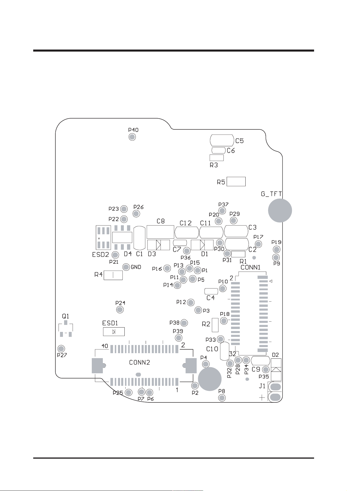
ⅤⅤ.. PPAATTTTEERRNN DDIIAAGGRRAAMM
44
1. PARTS ARRANGEMENT FOR EACH PCB ASS’Y
1) MAIN_TOM
SD500

45
ⅤⅤ.. PPAATTTTEERRNN DDIIAAGGRRAAMM
2) MAIN_BOTTOM

46
ⅤⅤ.. PPAATTTTEERRNN DDIIAAGGRRAAMM
3) KEY_TOP
47
ⅤⅤ.. PPAATTTTEERRNN DDIIAAGGRRAAMM
4) KEY_BOTTOM

48
ⅤⅤ.. PPAATTTTEERRNN DDIIAAGGRRAAMM
5) USB_TOP

49
ⅤⅤ.. PPAATTTTEERRNN DDIIAAGGRRAAMM
6) USB_BOTTOM

50
ⅤⅤ.. PPAATTTTEERRNN DDIIAAGGRRAAMM
7) FLASH_TOP

51
ⅤⅤ.. PPAATTTTEERRNN DDIIAAGGRRAAMM
8) FLASH_BOTTOM
C1
C12
C10
L1
C4
Q2
R13
R12
T2
C3
T1
R10
1
1
U1
R1
11
R4
SIP1

52
ⅥⅥ.. CCIIRRCCUUIITT DDIIAAGGRRAAMM
1. BLOCK DIAGRAM
{Key Board}
{USB Board}
{Main Board}
[Charge IC]
RichTek
RT9590
Strobe Charge Circuit
[Motor IC]
SANYO
LB1846M
[V Driver]
[AFE]
Panasonic
NN12030
[DSP]
Sunplus
SPCA535
Ready/Busy
Indicator
Self Timer
LED
Interface
Microphone
[SDRAM]
256Mbit
[LED]
USB1.1
Mode SW
(Capture/Playback/AVI)
Power Button
Shutter
[Key]
Card
Connector
Direction Key
OK/Menu/Del
Vide/Tele
Voice
{Shutter Board}
{Key Board}
Secure Digital Card
&
Multi Media Card
Image
FIX_LENS
[CCD Sensor]
Panasonic
MN39482
[Power IC]
Maxim
MAX1567
Power Supply Circuit
Battery - In
Alcaline x 2
[Crystal]
Main-27MHz
RTC-32.768KHz
NAND Flash
16MBytes
[TFT-LCD]
Casio
COM18T1824
(1.8")
{Key Board}
[EEPROM]
93C66
SYSTEM
CCD
TFT-LCD
FIX_Lens
->P1V8_SYS
->P3V3_SYS
->P12V_CCD
->P3V3_CCD
->N8V_CCD
->P12V_TFT
TFT_BL +
->
TFT_BL -
->P3V3_SYS
->P5V_SYS

53
ⅥⅥ.. CCIIRRCCUUIITT DDIIAAGGRRAAMM
1) CCD_MN39482
2. CIRCUIT DIAGRAM
A
4
1
2
CCD_V
CCD_V
H
R100
CCD-V
C10 2
3
CCD_V5B
CCD_V5A
CCD_V6
CCD_V
CCD_ V3B
CCD_V3
R0402
47R
R107
2
R0402
100R
Q100
C04 02
0.1uF
3
UMT
21
V6
1
2
3
4
5
6
7
8
9
V5B
V4
V3B
V2
V1
VO
V5A
V3A
SHORT
P
C0402
C109
NU/10
13
2SC4083
UMT3
CCDI N+
VCCD-VH
D3
D100
R0402
12
12
1SS355
R105
44
CCD\DIP18 \
SOD-323
D101
100K
Panasoni c 1/2.5"
TGGPIO40
1SS355
0402
R
CCDSUBCTRL
SOD-323
CCDSUBCTRL
U102
CCD_SUB
MN39482
H2
H1
HL
RG
R101
CCD-DIP18-MN39482
SUB
CSUB
VPT
PW
VOD
C113
0R
C103
0402
C
NC
C110
F
0.1u
C0402
100K
R106
NC/
18
17
16
15
14
13
12
11
10
R0402
F
1000P
R0402
CSUB
0402
C
D
SUB_CC
NC
C116
C0402
C114
NC
VLD3V CCD-V H
CCD-
0402
R
R109
0R
6
1Y
1A
U100
SN74LVC2G17
1
1
C_H
R0402
R102
0R
1
CCD_H
52Y4
2
VCC
GND
3
C_H2
R103
CCD_H2
2A
0402
R
R110
0402
0R R
C105
C104
SOT-26-0.65
0R
C106
C119
F
0.1u
0.1uF
0.1uF
10u/6V3
C0402
C0402 C0402 C0402
C0805
U101
SN74LVC2G17
R104
C120
103P
6
52Y4
1Y
1A
1
2
C_RG
R0402
0R
CCD_FR
0402
C
0402
R
VCC
GND
3
R111
2A
0402
NC
C
R0402
R108
1M
0R
F C115
C107
0.1u
C0402
4
5
SOT - 26 - 0. 6
VL
CCD-
3
21
56
SOT-26-0.65
V
TANT-B
C118
22uF/16
+
C101
0.1uF
CCD_H2
CCD_H1
24MHz
TGGPIO32
TGGPIO33
CCD_FR
C108
H
CCD-V
TGGPIO34
22uF/16V
TANT-B
+
F
C100
0.1u
C0402 C0402

54
ⅥⅥ.. CCIIRRCCUUIITT DDIIAAGGRRAAMM
VD_V1
CH
D
MS_I
N2
VD_V
6
TGGPIO
9
SW_COL
3
CHAR
GE
MS_I
N1
SW_COL
2
USB_LIN
K
SW_COL1
CHCCHD
SW_PLAY
C0402
CDS_CLCCD
C0402
PWR_DET
C0402C0402
SW_COL0
C0402
TGGPIO12
C0402
CDS_OBCLP
C0402
TGGPIO6
C0402
TRIGGER
C0402
SW_COL5
C0402
VD_V2
C0402
CDS_ADCCLK
C0402
VD_V5
C0402
R040
2R0402
C0402
CDS_BLKG
C0402
V7
C0402
READY
C0402
SW_COL4
C0402
VD_V4
C0402
D3V3_DSP
VD_V3
TGGPIO1
1
TGGPIO1
0
CH
C
A3V3_DSP
P1V8_D
SP
A3V3_DS
P D3V3_DSP
P1V8_D
SP
D3V3_D
SP
MICP
MICN
AGC
OPI
A_VREF
OPO
AGCOUT
LBAT
RTC3V3
GPI O15
GPI O14
READY_LED
GPI O12
GPI O11
TRAP
C0805
RESETb
R0402
USB_LINK
CHARGE
C0402
SW_COL4
C0402
SW_COL3
12
G_CA P
SW_COL2
MC_621
SW_COL1
R0402
SW_COL0
C0805
TRIGGER
D3V3_DSP
MS_IN1
CDS_BLKG
CDS_ADCCLK
CDS_OBCLP
CDS_CLCCD
PWR_DET
READY
MS_IN2
A3V3_DSP
VD_V6
VD_V5
P3V3_SYS
VD_V4
VD_V3
VD_V2
VD_V1
CDS_D9
CDS_D8
CDS_D7
CDS_D6
CDS_D5
CDS_D4
CDS_D3
CDS_D2
CDS_D
1
CDS_D
0
P3V3
CDS_D[0..9]
ROM_DQ2
NF_R/
B
GPI O
3
SOT-26
ROM_A2
SOT-26
C0402
ROM_DQ6
SD_CL
K
SD_D3
C0805
NF_WEb
#L
5#R7
SD_D2
#R10 #R13 #P5 #K15 #G5 #N15 #E14 #E13 #E9
#J
5#M5#R5
ROM_A1
#R11 #R15
SD_CD
#E11 #R8 #M15
ROM_DQ
5
12
D200
1SS
355
SOD-323
ROM_WE
N
20mi
l
15mi
l
15mil
RTC3V
3
R217
NC/O
R
SD_ D
1
P3V3_SY
S
ROM_OE
R0603
ROM_DQ4
ROM_DQ3
SD_PW_ON
ROM_DQ
0
MARCO_DET
Crystal Area Shielding
ROM_DQ1
NF_CE
b
SD_
CMD
SD_ W
P
ROM_A
0
ROM_DQ
7
SD_ D
0
GPI O
2
C0402
Y200
FSX-27MHz
XTAL-FSX-6M2
R0402
SUSPEND
C0402
R040
2
R0402
R0402
R0402
C0402
SW_COL5
R0402
12
Y201
32.768KH
z
XTAL-100SB
R040
2
C040
2
P1V8_DSP
GPI O 0
B1
9
GPI O 1
A1
9
GPI O 2
B1
8
GPI O 3
A1
8
GPI O 4
C1
7
GPI O 5
B1
7
OVSS 1
J9
OVSS 2
K9
OVDD1
L5
OVDD2
P5
DVSS1
K5
DVSS2
N5
DVDD1
J5
DVDD2
M5
OVSS 3
L9
OVDD3
R7
DVSS3
R6
DVDD3
R5
MD15
L3
MD14
L2
MD13
K1
MD12
K2
MD11
K3
MD10
K4
MD9
J1
MD8
J2
MD7
J3
MD6
J4
MD5
H1
MD4
H2
MD3
H3
MD2
H4
MD1
G3
MD0
G4
OVDD5
R1
3
OVSS 5
L1
1
CKE
N3
UDQM
M4
LDQM
N2
MWE
M2
CAS
M3
RAS
L4
SDCLK
L1
AVDD1
R8
AVSS1
R9
AGCOUT
F1
5
A_VREF
E18
OPO
E19
OPI
E17
AGC
E16
MICN
E15
MICP
D1
9
DVDD4
R1
1
DVSS4
R1
2
OVDD4
R1
0
OVSS 4
L1
0
SUSPEND
G2
OVDD9
E13
OVDD8
E14
OVSS 9
E12
OVSS 8
J1
0
DIGTV21
T8
DIGTV20W7DIGTV19V7DIGTV18U7DIGTV17T7DIGTV16W6DIGTV15V6DIGTV14U6DIGTV13T6DIGTV12W5DIGTV11V5DIGTV10
U5
DIGTV9T5DIGTV8W4DIGTV7V4DIGTV6U4DIGTV5T4DIGTV4W3DIGTV3V3DIGTV2U3DIGTV1W2DIGTV0
V2
OVDD7
N1
5
OVSS 7
J1
1
MA14
V1
MA13
U2
MA12
U1
MA11
T3
MA10
T2
MA9
T1
MA8
R4
MA7
R3
MA6
R2
MA5
R1
MA4
P4
MA3
P3
MA2
P2
MA1
P1
MA0
N4
DVDD6
E11
DVSS6
E10
OVDD6
R1
4
OVSS 6
K1
1
TRAP
J1
8
PRST
J1
9
XVSS2
G1
5
XTALRTCO
C1
8
XTALRTCI
C1
9
XVDD2
H1
5
XVSS1
J1
5
XTALI
D1
8
XTALO
D1
7
XVDD1
K1
5
UVDD
G5
DP
F1
DM
G1
UVSS
H5
V_VREF
V9
COUT
W1
0
RSET
V1
0
CBL
U1
0
CBU
T1
0
RGB0
T19
RGB1
R1
6
RGB2
R1
7
RGB3
R1
8
RGB4
R1
9
RGB5
P1
6
RGB6
P1
7
RGB7
P1
8
RGB8
P1
9
RGB9
N1
6
V1
T15
V2
W1
6
V3
V1
6
V4
U1
6
SG1 A
V1
1
SG3 A
T1
1
SG1B
U1
1
SG3B
W1
2
SUB
T1
3
FR
V1
5
FH1
W1
5
FH2
W1
4
MSHUTTER
T17
VSUBCTRL
V1
4
PBLK
T16
FS
U1
3
FCDS
V1
3
ADCLP
U1
7
OBCLP
U1
8
ADCK
U1
9
SEN
U1
4
SCK
T1
4
SDO
U1
5
UTMI0
D6
UTMI1
E6
UTMI2
A5
UTMI3
B5
UTMI4
C5
UTMI5
D5
UTMI6
E5
UTMI7
A4
UTMI8
B4
UTMI9
C4
UTMI10
A3
UTMI11
B3
UTMI12
C3
UTMI13
A2
UTMI14
A1
UTMI15
B2
UTMI16
B1
UTMI17
C2
UTMI18
C1
UTMI19
D4
UTMI20
D3
UTMI21
D2
UTMI22
D1
UTMI23
E4
UTMI24
E3
UTMI25
E2
UTMI26
E1
UTMI27
F5
UTMI28
F4
UTMI29
F3
UTMI30
F2
LDQS
N1
UDQS
M1
GPIO10
U9
GPI O 9T9GPI O 8W8GPI O 7V8GPI O 6
U8
SG5 A
V1
2
SG5B
U1
2
SG7 A
T1
2
SG7B
W1
3
BOUT
W9
ROUT
W1
1
V5
W17
V6
V1
7
V7
W1
8
V8
W1
9
V9
V1
9
V10
V1
8
FLASHCTR
T18
TESTMODE
N1
7
TGGPIO0
N1
8
TGGPIO1
N1
9
TGGPIO2
M1
6
TGGPIO3
M1
7
TGGPIO4
M1
8
TGGPIO5
M1
9
TGGPIO6
L16
TGGPIO7
L17
TGGPIO8
L18
TGGPIO9
L19
TGGPIO10
K1
6
TGGPIO11
K1
7
TGGPIO12
K1
8
TGGPIO13
K1
9
DVSS5
P1
5
DVDD5
R1
5
JTAG_TRSTb
J1
7
JTAG_CLK
J1
6
JTA G_T MS
H1
9
JTAG_TDI
H1
8
JTA G_T DO
H1
7
AUDP0
H1
6
AUDP1
G1
9
AUDP2
G1
8
AUDP3
G1
7
AUDP4
G1
6
AUDP5
F1
9
AVDD2
M1
5
AVSS2
L15
CHD
F1
8
CHC
F1
7
CHB
F1
6
FMGPIO0
C1
6
FMGPIO1
B1
6
FMGPIO2
A1
6
FMGPIO3
D1
5
FMGPIO4
C1
5
FMGPIO5
B1
5
FMGPIO6
A1
5
FMGPIO7
D1
4
FMGPIO8
C1
4
FMGPIO9
B1
4
FMGPIO10
A1
4
FMGPIO11
D1
3
FMGPIO12
C1
3
FMGPIO13
B1
3
FMGPIO14
A1
3
FMGPIO15
D1
2
FMGPIO16
C1
2
FMGPIO17
B1
2
FMGPIO18
A1
2
FMGPIO19
D1
1
FMGPIO20
C1
1
FMGPIO21
B1
1
FMGPIO22
A1
1
FMGPIO23
A1
0
FMGPIO24
B1
0
FMGPIO25
C1
0
FMGPIO26
D1
0
FMGPIO27
A9
FMGPIO28
B9
FMGPIO29C9FMGPIO30
D9
FMGPIO31A8FMGPIO32
B8
FMGPIO33C8FMGPIO34
D8
FMGPIO35A7FMGPIO36
B7
FMGPIO37C7FMGPIO38
D7
FMGPIO39
E7
FMGPIO40
A6
FMGPIO41
B6
FMGPIO42
C6
OVDD10E9OVSS 10
E8
TxD0
D1
6
RxD0
A1
7
SDCLKn
W1
U200
SPCA535A
ROM_DQ[0..7]
D3V3_D
SP
D3V3_D
SP
D3V3_D
SP
D3V3_D
SP
GPIO17
GPIO1
6
SD_ WP
SD_ CD
ROM_A[0..2]
SD_CMD
SD_ D2
NF_WEb
SD_D1
SD_D0
SD_CLK
SD_ D3
NF_R/B
NF_CEb
ROM_WEN
ROM_OE
RXD0
TXD0
MA14
MA1
0
MD5
MICP
MIC
N
AGC
MA1
OP
I
A_VREF
MD14
OP
O
AGC
OUT
LBAT
GPI O1
5
GPI O1
4
READY_LED
MA9
GPI O1
2
GPI O1 1
MA11
TRAP
TGGPIO15
VD_SG1
A
VD_SG3A
MD0
VD_SG3B
VD_SG5
A
VD_SG5
B
EE_CS
MD7
SH-LIGHT_EN
CDS_
SR
CDS_SVVD_SUB
MD2
CCDSUBCTRL
CCD_
H2
CCD_H1CCD_FR
MA13
CDS_SEN
CDS_SCK
CDS_SD
I
MD10
RES
ETb
MA3
MA6
MA1
2
MA8
MD1
5
MD1
3
BUZZER
MA4
MOTO_CS
USB_DE
Tb
SD_PW_ON
MD12
CCD_ON
MA2
MD6
MD1
1
MA5
MD9
MD3
MD1
TFT_BL_ON
MD4
MA7
MA0
TFBGA-288P
MD8
D3V3_DSP
D3V3_D
SP
P1V8_D
SP
P
214
P1V 8_ D
SP
A3V3_DS
P
D3V3_D
SP
A3V3_DS
P
D3V3_D
SP
CCD_ON
D3V3_D
SP
UDQM
USB_DETb
LDQM
CKE
BUZZER
MWRb
CASb
COUT
TFT_BL_ON
VD_SG1A
RASb
VD_SG3A
SDCLK
A3V3_DS
P
D-PLUG_DET
VD_SG3B
MA[0..14]
VD_SG5A
VD_SG5B
EE_CS
MD[0..15]
SH-LIGHT_EN
USB_DM
CDS_SR
USB_DP
CDS_SV
VD_SUB
CCDSUBCTRL
CCD_H2
CCD_H1
CCD_FR
CDS_SEN
CDS_SCK
CDS_SDI
C0402
C040
2
R040
2
C040
2
R040
2
R0402
C040
2
P1V 8_ DSP
ROU
T
TFT_CLK
BOU
T
TFT_D5
TFT_D4
TFT_D3
TFT_D2
TFT_CLK
TFT_SPI_CS
TFT_RST
HSYNC
VSYNC
D3V3_D
SP
P1V 8_ D
SP
TFT_D[0..7]
TFT_D1
TFT_D0
HSYNC
TFT_RST
TFT_SPI_CS
VSYNC
TFT_CLK
AP_IN1
AP_IN2
DIGTV14
DIGTV15
R0402
AP_IN1
AP_IN2
TFT_D6
TFT_D
7
RP4X2-0402
P218
TFT_SPI _SC K
TFT_SPI_DI
TFT_SPI _SC K
TFT_SPI_D
I
For CASIO 3G Interface
To Lens Input
To SDRAM
CKE
UDQM
LDQM
MWRb
CASb
RASb
SDCLK
D-PLUG_DET
USB_DM
USB_DP
COUT
P208
P
209
R203
10
0K
R200
0R
R208
2K
R204
1M
R205
33
R
R206
33
R
C230
20P
F
C231
20P
F
C232
20P
F
C233
20P
F
R207
33
R
P
203
P212
P201
P200
R210 22R
R211 22RR212 22R
R0402
1 2
3 4
5 6
78
PR200
22
R
1 2
3 4
5 6
78
PR201
22
R
C200
0.1u
F
C201
0.1uF
C202
0.1uF
C203
0.1uF
C204
0.1uF
C205
0.1uF
C212
0.1uF
C213
0.1uF
C214
0.1uF
C215
0.1uF
C216
0.1uF
C206
0.1u
F
C207
0.1uF
C208
0.1uF
C209
0.1uF
C210
0.1uF
C211
0.1uF
C217
0.1uF
C218
0.1uF
R201
10
0K
R202
100K
C224
0.1u
F
C229
10uF/10
V
C227
10uF/10
V
C228
10uF/10
V
C223
0.1u
F
C219 0.1u
F
C220 0.1uFR209 15
0R
C222
0.1u
F
R216
1K
R213
51
0R
TP20
0
TP20
1
R214
91K/8K
2
R215
18
0K
C221
0.1uF
C225
NC
P217
DIGTV8
P213
P
206
P
207
P
211
P20 2
MARCO_DET
GPI O 1
SW_PLAY
P221
P210
EE_SCK
EE_SDI
EE_SDI
EE_SCK
DRAMGPIO
4
P
223P222
L200
0R/10uH
INDUCTOR-R3.5MM
TANT-
B
P1V8_DSP
P1V8_SY
S
+
C226
100uF/6.3
V
SOT-26
C0402
C235
NC/0.1
uF
C0805
C234
10uF/10V
IN
1
SHDN
3
G
2
OUT
6
NC/BP
4
G
5
U203
NC/RT9193-18P
B
IN
1
SHDN
3
G
2
OUT
6
NC/BP
4
G
5
U201
RT9177-32P
B
IN
1
SHDN
3
G
2
OUT
6
NC/BP
4
G
5
U202
RT9177-32P
B
123
64
SOT-26
5
2) SPCA536 DSP

55
ⅥⅥ.. CCIIRRCCUUIITT DDIIAAGGRRAAMM
V
V
3) Image Peripheric circuit
A3
V
A3
C302
0.1uF
C0402
D3
D3V
F
C303
0.1u
C0402
10mil
V
6
4
OUT
IN
1
3
15mil 10mil
C327
SL
NC
NC
NC
NC
NC
9943
AD
R
PR300
22
10uF/10
C329
0.1uF
C0402C0805
26
NC/BP
SOT-
G
5
G
2
SHDN
R310
10k
V C310
C308
10uF/10
C0805
CCDIN+
C060 3
0.1u/25V
N
CCD_I
21
24
22
23
REFT
REFB
CCDIN
SDATA
SCK
GND
D0
1D12D23D34D45D56D67D78
1 2
3 4
5 6
78
CDS_D0
CDS_D1
CDS_D2
CDS_D3
P300
H
L-1008
L303
10U
32PB
U300
RT9177-
3
P3V
25
26
27
28
29
30
31
32
33
317P318P319
P
CDS_SEN
CDS_SDI
CDS_SCK
CDS_SDI
CDS_SCK
CDS_SEN
TGGPIO37
TGGPIO39
TGGPIO38
0402
R
CCD_ON
2K
R0402
R309
1.
P
NU/104
C319
V
A3
17
18
20
19
SHP
SHD
AVSS
AVDD
AD9943
1 2
3 4
5 6
78
CDS_D4
CDS_D5
CDS_D6
CDS_D7
303P302P301
P
10mil
C311
10uF/10V
C0805
L-1008
L302 0R
V
C0805
C309
10uF/10
L300
DCCD-VH
P12V_CC
C0805
C304
10uF/16V
F
C0402
10mil
C300
0.1u
L-1008
0R
10mil
L301
CCD CCD-VL
N8V_
C0805
C312
10uF/10V
F
C0402
10mil
C301
0.1u
1008
L-
0R
10mil
5
123
64
SOT-26
CCD_ON
Hz
TGGPIO29
TGGPIO14
24MHz
24M
CDS_SV
CDS_SR
0402
0402
R
R
R
R
C322
1uF/10V
C0603
0603
C321
1uF/10V
C
PBLK
CLPOB
DVSS
DATAA CLK
DVDD
DRVSS
DRVDD
D9
D8
R
PR301
22
307P306P305P304
P
R304 47
R303 47
C305
C306
5
U301
QFN32P-0.
16
15
14
13
12
11
10
9
V
D3
R0402
R0402
R
R
22
R300
R307 22
R308
D9
CDS_D8
CDS_
309
P
P30 8
CDS_OBCLP
CDS_CLCCD
0402
R0402
R
R
R
NC/0
R302 0
R305
0402
C
NC
C0402
NC
C307NCC0402
0402
R0402
47R
R301
0R
R
CDS_BLKG
24MHz
CDS_ADCCLK
TGGPIO43
TGGPIO44
VD3VD3V
A3
TGGPIO31
VD_V3
VD_V1
VD_SG1A
4
CCD_V 6
CCD_V3A
CCD_V5A
CCD_V3B
CCD_V5B
CCD_V
VD_V1
VD_SG1A
VD_V3
CCD_V 1
CCD_V 2
P311 P312 P313
9
14
U302
OV810OV711OV412OV513OV3
OV6
OV2
15
OV1
16
VM
17
VL
18
VDC
19
IV1
20
CH1
21
IV3
22
CH2
L
V
D3
CCD-V
C315
0.1uF
C0402
C314
0.1uF
C0402
0402
C313
0.1uF
C
CH324IV225IV426IV627IV5
23
OSUB
VM
VL
VHH
VH
ISUB
CH5
CH4
28
0402
C
C318
0.1uF
V
D3
0402
H
C316
0.1uF
C
CCD-V
0402
H
C317
0.1uF
C
CCD-V
TGGPIO35
TGGPIO19
TGGPIO18
VD_SUB
VD_SG5B
VD_SG5A
CCD_SUB
VD_SUB
VD_SG5B
VD_SG5A
0805
C328
1uF/35V
C
+
P
AN20101A
QFN-28
8
7
6
5
4
3
2
1
L
H
CCD-V
CCD-V
L
C324
0.1uF
CCD-V
L
C323
0.1uF
CCD-V
5
VD_V
0402
C
0402
C
6
TGGPIO27
TGGPIO26
TGGPIO28
TGGPIO30
TGGPIO17
TGGPIO1
VD_V5
VD_V6
VD_V4
VD_V2
VD_SG3B
VD_SG3A
VD_SG3A
VD_SG3B
VD_V2
VD_V4
VD_V6
314 P315 P316 P333 P334 P335 P320 P321 P322
P

56
ⅥⅥ.. CCIIRRCCUUIITT DDIIAAGGRRAAMM
4) SDRAM_TRAP_EEPROM
MD13
MD15
MD14
MD[0..15]
R
RP4X2-0402
PR402
47
1 2
3 4
5 6
R
P3V3_SD
54
53
52
Vss
VssQ
DQ15
Vcc
DQ0
VccQ
U401
SDRAM-64MB/128MB/25
1
2
3
R
P3V3_SD
SDRAM(64M/128M/256M/512M)
R
PR40 7
47
1 2
MD0
RP4X2-0402
R
PR40 8
47
3 4
5 6
78
MD1
MD2
MD3
MD7
MD10
MD11
MD12
R
PR40 3
47
1 2
3 4
5 6
78
51
50
49
48
47
46
45
VssQ
VccQ
DQ14
DQ13
DQ12
DQ11
DQ10
DQ1
DQ2
VssQ
DQ3
DQ4
VccQ
DQ5
4
5
6
7
8
9
10
1 2
3 4
5 6
78
0402
S
RP4X2-
MD9-S
MD8-
MD4
MD5
MD8
MD9
MD[0..15]
48M Hz(SHORT)
MD7-S
MD6-S
MD6
UDQM
SDCLK
RP4X2-0402
R0402
R
78
0402
C
C
MD9-S
MD8-S
C408N
44
43
42
41NC40
39
38
37
Vss
CLK
DQ9
DQ8
VccQ
UDQM
DQ6
VssQ
DQ7
Vcc
LDQM
WE
CAS
11
12
13
14
15
16
17
18CS19
MD6-S
MD7-S
LDQM
MWRb
CASb
MA11
MA12
CKE
PR404
0402
R0402
R
R
S
R402 22RR401 22
R403 22
MA9-
36
35A934
A12
A11
CKE
BA020BA121A1022A023A124A225A326Vcc
RAS
MA13-S
MBA0
SDRAM_CSb
R
PR400
22
RASb
MA8
MA4
MA7
R
22
1 2
3 4
5 6
78
MA0-S MA0
MA5-S
MA6-S
33
32A631
30
29
A8
A7
A5
MA10-S
MA0-S
S
MA5-
RP4X2-0402
1 2
3 4
5 6
78
MA5
MA3
MA1
MA2
28
A4
Vss
27
PR40 1
0402
RP4X2-
R
22
TSOP54P
MA13-S
MA10-S
MA9-S
1 2
3 4
5 6
MA13
MA10
MA9
MA6-S
0402
RP4X2-
78
MA6
0402
C407
0.1uF
C406
0.1uF
)
C405
0.1uF
C404
0.1uF
C403
0.1uF
C401
RP3V3_SYS P408
P3V3_SD
P3V3_SDRP3V3_SDR P3V3_SDR P3V3_SDR P3V3_SDR P3V3_SDR
R
P3V3_SD
0.1uF
C0402 C0402 C0402 C0402 C0402 C
F
0402
C400
0.1u
C
F
C402
0.1u
C0402
Close SDRAM POWER ( VCC & VCCQ
MA[0..14]
K
SOT-25-0.65
Q400
UMC2N
3 4
IO-TRAP
S
P3V 3_ SY
123
54
SOT-25-0.65
22K
22
10
R1R2R3
PR40 5
12345 6
5 1
12233
1
R406
il
b
12233
SDRAM_CS
1
R412
MA0
MA1
MA8
MA4
MA3
MA5
789
R5R6R7
R8PP
R4
K
22
22K
TRAP
0R
R0402-3P
TRAP
MA6
MNR15
10K
2
MA7
MA2
MA13
MA12
MA14
PR40 9
1 2
3 4
5 6
78
10K
R404 10KMA9_J
MA9_J
0402
RP4X2-
0R
0402
R
TRAP
MA9
MA11
PR40 6
1 2
3 4
12233
0402
R
R405
10K
MA10
10K
RP4X2-0402
5 6
78
1
R409
0R
R0402-3P
12233
1
R410
MA12
MBA0
12233
1
R411
SDRAM SEL
0R
R0402-3P
V
10m
C0805
C409
10uF/10
L400
0R/10UH
L-1008
15mil
S
FBGA5 4-CM O
R0402
U400
C410
8NC7
VCC
CS
1SK2DI3DO4
EE_CS
EE_SCK
EE_CS
EE_SCK
F
0402
0.1u
C
6
5
ORG
GND
AT93C66
SOP-8
I
EE_SD
EE_SDI
S
P3V3_SY
MA14
100K
0R
R400
EEPROM
7
TGGPIO20
DIGTV16
DIGTV1

57
ⅥⅥ.. CCIIRRCCUUIITT DDIIAAGGRRAAMM
5) FlashROM-NandFlash-SD
SD_D3
SD_D0
SD_D1
SD_D2
SD_CD
SD_CLK
SD_WP
SD_CMD
S
P3V3_SY
3_SD
P3V
0402
R505
10K
R
10K
R504
5
k
PR502
10
MNR1
P
R4R5R6
7
R3
R7
8
R2
R8
9
R1
P
10
123
54
SOT-25-0.65
0402
R
PSD_D0
1
2
SD_D
SD_CD
SD_D
SD_W
9
8
11WP12
10
CD
GND
SD_CIM-F23R
DATA2
DATA1
G
13
CMD2GND3VDD4CLK5GND6DATA
CD/DAT3
SD500
SD/MMC
1
5 6
4
3
2
1
7
3_SD
P3V
3
MD
SD_C
SD_D
P3V 3_SD
0402
C505
0.1uF
C
4
5
Y
VCC
/SOT-25-0. 65
NC
GND
U502
SN74LVC17DCK
1A2
3
K
SD_CL
P
1
2
3
D
MD
SD_D
SD_C
SD_D0
SD_W
SD_D
SD_C
SD_D
NF_REb
ROM_OE
ROM_WEN
ROM_DQ[ 0.. 7]
ROM_OE
ROM_WEN
ROM_DQ0
ROM_DQ1
ROM_DQ2
NF_ALE
NF_CLE
509P510P512P511P513P514P515P516P517P518P519
P
_D6
_D4
_D7
_D5
R507
NF
NF
NF
NF
ROM_DQ4
ROM_DQ3
1 2
3 4
PR500 22R
NF_D1
NF_D0
R
NC/0
ROM_DQ6
ROM_DQ5
5 6
78
NF_D2
NF_D3
ROM_DQ7
ROM_A0
ROM_A1
ROM_A2
1 2
3 4
5 6
78
PR501 22R
NF_D4
NF_D5
NF_D6
NF_D7
_D3
_D0
_D1
NF
NF_D2
NF
NF
ROM_A [0. .2]
123
54
SOT-23-5P
P3V 3_SD
U500
F
C504
22P
C0402
R
R500
22
R0402
K
SD_CL
F
C500
0.1u
C040 2
1NC3
OUT
G
2
IN
AAT4250
SOT-23-5P
5ON4
V
S
P3V 3_ SY
C0805
C501
10uF/10
10mil 10mil
N
SD_PW_O
SD_PW_ON
SP3V 3_ SYSP3V 3 _S YS
P3V 3_ SY
48
NC
2NC4NC3NC1
40NC39NC38
37
41
I/O643I/O542I/O4
R/B7RE8CE9NC
B
1
NF_R/
SD_D
NF_REb
NF_R/B
NC
10NC11
b
12233
1
NF_CE
R506
0R
NF_CEb
36NC35NC34NC33
Vss
Vcc
Vcc12Vss13NC14NC15CLE16ALE17WE18WP
44
NC45NC46NC47NC
I/O7
NC
5SE6
R0402
10K
R503
0402
R502
10K
R
0402
R
R501
10K
29NC28NC27NC26NC25
I/O332I/O231I/O130I/O0
P
NC
NC
U501
K9F2808U0A
TSOP-48
19
20NC21NC22
24NC23
b
DQ0
DQ1
ROM_
ROM_
LE
NF_ALE
NF_C
500
P
S
C503
104P
NF_WE
NF_WEb
C040 2
P3V 3_ SY
S
C502
104P
C0402
P3V 3_ SY

58
ⅥⅥ.. CCIIRRCCUUIITT DDIIAAGGRRAAMM
6) USB1.1_MIC_TVOUT_BUZZE
R609
1%
10K
R0402
VBAT 1
AGCOUT
F
0402
C602
0.1u
C
LBAT
AGC
C610
R612
3
10uF/6V
470K
C0805
R0402
MI CP
MI CN
1%
R605
R610
C600
15K
0.1uF
R0402C
0402
10K
R0402
R611
1%
249K
R0402
C608
MIC2
C612
V
C0402
0.47uF/10
V
C611
0.47uF/10
C0402
MIC1
C0402
C609
3
C0805
10uF/6V
F
330P
P604
OPI
P603
OPO
A_VREF
3
2 1
UMT3
C614
22P
C0402
COUT
T
COU
L601
TV
H
1.8u
C615
0805
L
C613
R613
330P
270P
75R
0402
C0402 C
R0402
S
BUZ600
BUZZER
V
47uF/6.3
TANT-A
+C605
2
10K
Q600
DTC143XUA
UMT3
13
1
1
2
TP602
BUZZER
L0805
R608
R607
1
NC/0R
0R
R0402-3P
12233
P
1
0R
P5V_SY
12233
1
R606
4
6
VS25VS1
VDD
GND2RST
VSO
1
3
S P1V8_SYS
R604
10K
R0402
P3V3_SY
C601
U600
12233
F
0.1u
C0402
RT9801B
SOT-26
0R
R0402-3P R0402-3
R6141KR
0402
4.7K
26
5
2 31
SOT-
6 4
1
601
TP
RESETb
Buzzer

59
ⅥⅥ.. CCIIRRCCUUIITT DDIIAAGGRRAAMM
59
7) INTERFACE IO
TFT_BL-
TFT_BL +
+
#2
#1
IDC40-0.5-MA
A
CONN700
BTB-40PIN_MAL E
IDC40-0.5-M
P726
TFT_BL-
1 2
+
TFT_BL
P702
P701
T
P12V_TF
S
P3V3_SY
#39 #40
P727
VSYNC
S
P3V3_SY
P12V_TFT
3 4
5 6
7 8
9 10
S
P12V_TFT
P3V3_SY
TFT_SPI_DI
P703
P705
TFT_RST
TFT_SPI_SCK
P728
TFT_D6
11 12
TFT_SPI_CS
P704
P729
HSYNC
13 14
TFT_D7
P706
P730
N
BL_O
15 16
TFT_CLK
P707
P731
TFT_D4
17 18
5
TFT_D
P708
TFT_BL
P732
2
TFT_D
19 20
3
TFT_D
P709
TFT_BL-
P733
0
TFT_D
21 22
1
TFT_D
P710
P734
D0
23 24
RXD 0 T X
P711
TFT_CLK
TFT_SPI_CS
TFT_RST
HSYNC
VSYNC
TFT_SPI_SCK
TFT_SPI_DI
K
S
K
RSTSW_COL0_A
TFT_
TFT_SPI_DI
TFT_SPI_SC
TFT_CL
TFT_SPI_C
1
0
DIGTV19
DIGTV11
DIGTV18
DIGTV2
DIGTV2
P736
P737
P738
W
USB_L INK
SW_COL0SW_COL1
MA9_J
TV
PWR_S
25 26
27 28
29 30
31 32
33 34
35 36
OL4
OL3
SW_COL2
SW_C
SW_C
P713
P714
P715
P716
P717
C
HSYN
DIGTV10
D
READ Y_LE
SW_PLAY_ ON
C
VSYN
DIGTV9
37 38
P718
5
6
7
TFT_D
TFT_D
TFT_D
DIGTV5
DIGTV6
DIGTV7
39 40
TFT_D[0..7]
SW_COL0
SW_COL1
SW_COL2
0
1
2
3
4
TFT_D
DIGTV4
OL0
OL1
OL2
SW_C
TFT_D
TFT_D
TFT_D
DIGTV1
DIGTV2
DIGTV3
SW_COL3
TFT_D
SW_C
SW_C
TGGPIO0
TGGPIO1
TGGPIO2
TGGPIO3
DIGTV0
P751
SYS1P3V3_SYS
2
4
P5V _
+
+
CONN701
1
3
SH-LIGHT_EN
SW_COL3
OL4
SW_C
TGGPIO4
USB_LINK
6
+
+
5
MA9_J
P719
SW_COL4
SW_PLAY
TGGPIO5
USB_DP
8
+
+
7
MS_IN1
P720
SW_PLAY
P741
USB_DM
10
+
+
9
MS_IN2
P721
MARCO_DRT
P742
USB_DETb
12
+
+
11
AP_IN1
P722
MARCO_DRT
BL_ON
P743
MARCO_DET
14
+
+
13
AP_IN2
P723
BL_ON
W
PWR_S
P744
16
+
+
15
P724
PWR_SW
RESETb
18
+
+
17
RESETb
READY_LED
READY_LED
USB_L INK
TGGPIO13
G PI O13
R701
47K
P750
8
+
+
IDC1
M
TEST POINT BOTTO
USB_L INK
MA9_J
MA9_J
0402
R
IDC18-0.5-FA
RXD0
TXD0
RXD0
TXD0
PAD701
PAD702
PAD703
PAD704
PAD708
PAD705
RS232
0
S
TV
D-PLUG_DET
TXD0
RXD
P3V3_SY
M
TEST POIN T BOT TO
P700
RESETb
TRIGGER
747
746
355
SOD-323
D701
NC/1SS
P
P
P725
P
6
CONB064-16
SIP700
SIP1
READY
CHARGE
S
P752
P753
12
P5V_SY
GE
MI C1
MI C2
TRIGGER
READY
CHAR
123456789101112131415
1
5
234
S
P3V3_SY
6
SW_COL0_A
789
SW_COL2
1
VBAT
PWR_SW
101112
13
14
_05C
OL5
SW_C
70-6
SC
ESD701
NC/ESD_SMF
3 4
5
6
2
1
-2
OL5
OL4
OL2
OL0
OL1
SW_C
SW_COL3
SW_C
SW_C
SW_C
MNR15
PR700
PR-10P8R
near CONN702
ESD
5 6
16
S
P3V3_SY
P
R4R5R6
7
8
9
10
4
R3
R7
3
2
R2
R8
P
1
R1
15
16
CONB064-16P TOP VIEW
SW_C
12
8V
R0603
ESD700
NC/RSB6.
SW_COL1
SW_COL2
SW_COL3
SW_COL4

60
ⅥⅥ.. CCIIRRCCUUIITT DDIIAAGGRRAAMM
60
8) POWER_MAX1567
807
P
C830
10uF/6.3V
20mil
+
3V
8
L-100
L809
10uH
TANT-A
C816
10uF/6.
+
31
2
R804
C826
20mil
+
20mil
R0402
R830
330K 1%
FBSU
Q806
V
P5
P5V_SYS
S1
P5V _SY
AO3401
SOT-23
C0402
C803
TANT-A
V
15mil
C831
22uF/6.3
C1206
+
P1V8_SYS
15mil
R823
SCF
100K
R0402
C1210
47uF/10V
F
C835
NC/470P
0402
R
ND
R831
110K 1%
NG
L806
10uH
C0402
L-ELL4LM
15mil
LXSD
90.9K 1%
R0402
R832
R0402
2 K 1%
40.
F
FBSD
C0402
C834
NC/470P
T
1
BAT
805
P
0.1uF
1
PAD800
PAD
PAD
BAT800
AA
D
PAD801
PA
PAD1
SIP2
BATT
AA
P5V_SYS
P12V_CCD
P12V_TFT
L-1008
L805
10uH
1
Q801 B
UPA508TE
7uH
L-ELL4LM
L800
4.
VBAT1
T
BAT
F
C0402
C821
4700P
R825
FB2
DL2
DL3
DL1
P5V
FB3L
CC3
P800
100K
R801
F
R812
0
R0402
C818
3300P
C0402
TFT_BL_ON
TFT_BL_ON
15mil
L-1008
L808
10uH
R834
NU/6.8K
B
TANT-
C806
22uF/16V
+
R806
R805
1M 1%
R0402
15mil 15mil
+
V
1210
C805
C
10uF/16
34
Q801A
52
15mil
1
C0805
C807
10uF/10V
n
C814
10uF/10V
P3V3 V i
30mil
N
7uH
L802
4.
CCD_O
R815
0
R0402
2K
0402
8.
R
1567
U801
MAX
QFN-40P
31
32
33
34
35
36
37
38
39
40
10K
R817
R0402
F
R0402
C819
1000P
C0402
1
3
2
R0402
115K 1%
R0402
1
95
SOT-25-1-0.
UPA508TE
C0805
L-ELL4LM-L
LXM
20mil
PVM
CC2
28
29
30
CC2
ON2
FB2
INDL 2
GND
DL2
DL3
DL1
PV
CC3
FB3L
ON3
FB3H
CC12FB13ON14PGSD5LXSD6PVSD7ONSD8FBSD9CCSD
1
CC1
FB3H
FB1
801
P
SOT-23
AUX1
1
FB1
DL
n
C815
10uF/10V
C0805
T
P5V Vi
L
BAT
30mil
7uH
L-ELL4LM-
L803
4.
12
SOD-123
D804
R0402
R813
0
P5V
20mil
B130LAW
R826
51KC827
R0402
LXSU
100pF
C0402
C
K
OS
SDO
21
22
23
24
25
OSC
PGM26LXM27PVM
AUX1OK
PGSU
PVSU
LXSU
SDOK
SCF
ONSU
FBSU
CCSU
REF
ONM
FBM
CCM
SUSD
10
il
15m
LXSD
C0805
C813
10uF/10V
FBSD
V
P5
R814
0
PWR_ON
N
PWR_O
P5V_SYS
R803
100K
R0402
F
SC
20
19
18
17
16
15
14
13
12
FBM
11
CCSU FBSU
V
CCM
P5
CCSD
R818
C820
R816
0
C828
F
RE
R819
47K
R0402
F
C822
4700P
C0402
123
54
R0402
F
0.1u
C0402
33K
R820
68K
R0402
R0402
F
F
6800P
C823
0.01u
0402
C0402
C
SOT-25-0.95
N
N
CCD_O
PWR_O
CCD_ON
R835
NU/6.8K
R0402
12
V
CCD
N8V_
8
L807
10uH
L-100
E
Q803 B
UPA507T
15mil
E
B
TANT-
C812
47uF/10
+
15mil
%
R808
R0402
R0402
R807
549K 1%
90.9K1
15mil
V
34
1210
C808
10uF/10
C
52
15mil
7uH
L801
4.
AUX2
R809
562K 1%
R0402
15mil
1
Q802 B
34
L-ELL4LM
UPA508TE
15mil
1
SOT-25-1-0.95
Q803A
UPA507T
L804
33uH
L-ELL4LM
S1
DL2
FB2
REF
P5V _SY
15mil
C809
C0805
10uF/10V
VBAT1
P3V 3_ SYS
15mil
6
OUT
32PB
IN
U800
RT9177-
1
20mil
P3V3
R0805
0R
31
SOT-23
Q805
AO3401
20mil 20mil
M
PV
TFT_BL-
TFT_BL+
15mil
V
1206
C
C817
22uF/10
52
1
C810
10uF/10V
C829
10uF/6.3V
C0805
C804
0.1uF
4
NC/BP
G
G
SHDN
3
R827
+
R821
R0402
165K 1%
C0402
SOT-26
5
2
GPI O 14
PWR_SW
PWR_ON
PWR_ON
C802
0.1uF
802
P
B
C824
47u/6.3V
TANT-
2
R0402
R802
100K
+
C825
C1210
47uF/10V
R822
FBM
C833
Q807
K
SDO
T
BAT
9K 1%
ND
90.
R0402
NG
F
C0402
NC/470P
22K
SOT-25-0.65
22K
UNC2N
5 1
3 4
F
C0402 C0402
C800
0.1u
PWR_DET
P80 3
ON
PWR_SW-T
22K
2
22K
PWR_SW
PWR_DET
TGGPIO22
2
SW_ PL A Y _
PWR_K EEP G PIO14
SOT-23
D803
DAN202K
3
1
3
D805
DAN202K
SOT-2
2
3
1
R824
R0402
22K
P806
F
C0402
C801
0.1u
P3V 3_ SYS
2
F
R040
R833
22K
P3V 3_ SYS
R0402
R810
10
C0402
C832
0.1u
Y
SW_PLA
R0402
R811
100K 1%
1
SOT-25-1-0.95
Q802A
UPA508TE
AUX3
TVBAT1
FB3H
DL3
C0805
BAT
FB3L
ND
808
P
NG
01R800
31
Q804
IRLML64
40mil
UMT3
SOT-23
Q800
DTC143XUA
2
4.7K
R0402
100K
13
10K
2
40mil
C811
10uF/10V
C0805
PWR_ON
61
ⅥⅥ.. CCIIRRCCUUIITT DDIIAAGGRRAAMMⅥⅥ.. CCIIRRCCUUIITT DDIIAAGGRRAAMM
C0402
D1
RB501V- 40
TFT-CON
13579
1
11315171921232527293133
246
8
1
012141618202224262830
32
CONN1
FPC54393-33P FOR Z 515
C2
10U/10V
R1 10K
C0805
VCDC
VCAC
R0402
TFT_D1
TFT_D3
TFT_D5
TFT_D7
TFT_CLK
TFT_SPI_CS
TFT_SPI_SCK
TFT_SPI_SDI
TFT_D0
TFT_D4
TFT_D2
VSYNC
TFT_D6
HSYNC
TFT_RSTBL_ON
R2
560K
R0402
C1
10U/10V
C0805
VCDC
P3V 3_ SYS
C6
0.1uF
VGH
P12V_TFT
C0402
C7
0.1uF
C2+C2-
C0603
C9 1U/25V
C0603
C10 1U/ 25V
C2-
VGL
C1+ C1-
C1-
VBCVSH
VCAC
C3
10U/10V
C0805
VVCOM
C0805
C11
2.2U/25V
P12V_TFT
D2
RB501V- 4
0
D3
NU/RB501V-40
C1206
+
C8
4.7U/25V
VGL
VCOM
TFT_BL +
TFT_BL -
1
2
J1
LED_BL
P17
VCDC
VGH
C2+
C2-
VGL
C1+
C1-
VBC
VSH
VCAC
VVCOM
VCOM
P18
P19
P20
P28
P29
P30
P31
P32
P33
P34
P35
SW_ CO L 0
SW_ CO L 1
SW_ CO L 2
SW_ CO L 3
SW_ CO L 4
SW_COL1_A
SW_ CO L 0 _A
61
D4A
IMN10
SOT- 2 6
SW1
UP
KEY-METAL_DOME-4
52
D4B
IMN10
SOT- 2 6
SW7
RIGH T
KEY-METAL_DOME-4
SW1 1
Zoom_Out
KEY-METAL_DOME-4
SW3
OK/ ENT ER
KEY-METAL_DOME-4
SW6
LEFT
KEY-METAL_DOME-4
SW2
DOWN
KEY-METAL_DOME-4
SW1 0
Zoom_IN
KEY-METAL_DOME-4
43
D4C
IMN10
SOT- 2 6
SW4
LCD
KEY-METAL_DOME-4
SW8
DEL
KEY-METAL_DOME-4
P21
P22
P23
P24
P39
P25
P40
P26
P3V3_SYS
TFT_D1
TFT_D3
TFT_D5
TFT_D0
TFT_D4
TFT_D2
TFT_BL + TFT_BL-
SW_ CO L 3
SW_COL0_A
SW_ CO L 4
SW_ CO L 2
SW_ CO L 1
READ Y_L ED
SW_ CO L 0
1 2
3 4
5 6
7 8
910
1
11213141516171819202122232425262728293031323334353637383940
CONN2
BTB-40PIN_Female
IDC40- 0.5-FA
P12V_TFT
P3V 3_ SY
S
To Main Board
TGGPI O2
TGGPI O4
TGGPI O3
TGGPI O1
[BottomSide]
GPIO13
TGGPI O0
P12V_TFT
P3V3_SY
S
P12V_TFT
P1P2P3
P10P5P12
P9P4P11
P6 P14
P7 P15
P8 P16
TFT_D7
VSYNC
TFT_CLK
TFT_SPI_CS
TFT_D6
HSYNC
TFT_RSTTFT_SPI_SCK
TFT_SPI_SDI
BL_ON
P13
P12V_TFT
P3V 3_ SYS
P12V_TFT
P3V 3_ SYS
P36
P37
P38
READ Y_L ED
R3
200R
R0402
4.7K
10K
2
13
Q1
DTC143X UA
UMT3
LED-SMT-321
5
GPI O13
P3V 3_ SYS
P27
12
LED1
GREEN
GND_ESD GND_ESD
SC70-
6
SW_ CO L 3
SW_ CO L 4
SW_ CO L 2
SW_ CO L 1
SW_ CO L 0
C0402
C4
1uF/6.3
V
C0805
C12
4.7uF/16V
C0805
C5
FPC54393-33PFOR Z515
SOD- 3 23
SOD-323
TFT-CON
1
2
3 4
5
6
ESD2
NC/ESD_SMF_05
C
SW9
MODE
KEY-METAL_DOME-4
SW5
PL AY
KEY-METAL_DOME-4
SW_PL A Y
SW_ PL A Y
12
ESD1
NC/RSB6.8
V
R4
NC/0
R
R0603
GND_ESD GND
R5
NC/0R
R0603
GND_TFT
G_TFT
9) CASIO 1.8 inch 3G Panel

62
ⅥⅥ.. CCIIRRCCUUIITT DDIIAAGGRRAAMM
10) D402 LENS_USB
USB_L INK
USB_LI NK
P7
2
SOT -2 3
Q1
DTB113ZK
K
1K
10
P3V3_SYS
USB_DP
USB_DM
USB_DETb
F
USB_DP
USB_DM
P8
USB_DETb
2
R0402
R040
R8 47K
R10 27 R
K
R4
1.5
31
R11 27 R
R0402
K
R0402
R3
NC/470
C5
0.1u
R9
47K
R0402
C4
R7
NC/100K
R0402
C3
K
R0402
R6
NC/100
4
1
2
C040
R0402
F
10P
F
10P
P11
P14
P12
P13
USB_DP
USB_DM
USB_DETb
USB_LI NK
MA RCO_DET
10
2
4
6
8
12
14
16
P5V _SY SP3V3_SYS
+
+
+
+
+
C0402C0402
+
CON1
1
3
5
7
SH- L IG HT _EN
MS_IN1
MA 9_J
P9
P10
18
+
+
+
+
9
1
1
MS_IN2
AP_IN1
TP1
TP2
8
+
+
+
+
+
+
+
+
IDC1
3
1
AP_IN2
TP3
IDC18- 0.5-MA
5
7
1
1
TP4
B2
CMFW2012M
U_P4
U_P3
U_P2
U_P1
P2P3P4P5P6
U_P4
BEAD
B3
U_P5
2
U_P3
U_P1
U_P2
1D-2D+3NC4
U_P5
VCC
SHE L L
L0603
BEAD
3
5
GND
CM FW2012M
C2
C1
B1
F
20P
20PF
BEAD
D
BEA
CON2
123
OUT 4
L0603
R0805
R5
0R
4
OUT
C7
0.1uF
SI P4
4
FPC-CON04-P0.5-A
OUT 1
OUT 2
OUT 3
OUT 1
OUT 3
C0402
OUT 2
C8
0.1uF
C0402
P
20mil
MA9_J
P1
0
R0402
R1
20
12
P3V 3_ SYS
Q2
DTC143X UA
UMT3
4.7K
2
LED-SMT-2520
LED1
RED
SH- L IG HT _EN
USB-MIN I-5
USB1
USB_M INI5
13
3
21
Focus L ight
UMT3
10K
6
10
GND
OUT 27OUT 18OUT 39OUT 4
M
VCC
IN42IN33IN14IN2
MARCO_DET
K
R0402
R12
10
P3V 3_ SYS
UP
S1
Marco
SW-1AB-420-T35
12
P5V _SY S
U1
D1
RB411D
23
LB 1846
1
SOT- 2 3
MS_IN2
MFP10S
5
+
MS_IN1
AP_IN1
AP_IN2
AP_IN1
MS_IN1
MS_IN2
CASE-B
C6
22uF/10V
AP_IN2
SH- L I GHT _ EN

63
ⅥⅥ.. CCIIRRCCUUIITT DDIIAAGGRRAAMM
11) D402Shutter_Strobe
P
ST B1
PAD 1
TP3
TUBE_
TRG
10mil
P13
1
P5
3
D1
GS3004S
2
St r ob e
P3
10mil
R0402
R13
40mil
0.01uF/500V
C1210
1
H
P
CAP_
TP4
47R
R0402
R12
220R
10mil
4
40mil
1
1
3
Q2
GT8G13
SO-8
6
TR0496-H
T2
TR049
P
20mil
2
S
CAP-N
120uF/330V
TP6
PAD 1
PAD 1
P2
R
R0805
R11
0
MIC1
MI CROPHONE1
E-M IC2
V
ESD3
NC/RSB6.8
EMD 2
12
P6P7P8
P9
P12
P10
ESD4
EMD 2
NC/RSB6.8V
12
P11
2
MIC1
MIC
C9
NC
TRIGGER
CHA RGE
P3V3_SYS
SW_ CO L 2
PWR _SW
SW_COL0_A
C7
1000PF
C0402
READ Y
R0603
R2
100K
ST ROB E TU B E
TP2
TUBE_TRIG
10mil
SMA
D2
QG5395SA
PAD 1
TP5
TUBE-N
12
10mil
PAD 1
R8
+
M
R0805
1
C5
0.01uF/500V
5
62
7
8
C1206
10mil
C4
+
10mil
3
40mil
SOT- 2 3
R1206
R6
C0402
300K
P5V _SY S
R20
3.3K
R0402
Short
R0402
R19
NC
F
C0402
C2
0.1u
40mil 30/40mil
5
4
T1
TRANS-F15
1
TR_EPC6.2
C11
NC
3 6
2
R0603
R10
931
2
R17
1K
R0402
R16
1K
F
C12
100p
C0402
K
R14
1
R0402
R040
+
C6
47uF/4V
TANT-B
C0402 C0402
C8
NC
R0402
R15
1K
ESD2
NC/RSB6.8S
12
31
CASE-B
C1
47uF/4V
+
2
SOT- 2 3
Q1
AO3400
TP1
9
St r ob e
0
1
2
1
1
1
P4
R0603
R9
2M
P3V 3_ SYS
Sho r t
U1
20KR410K
VBAT2
P1
R0603
R1
100K
H
L1
10u
L-ELL4LM
8
7
6
5
R0603
R0603
R3
IMCD
VDRV
VDOUT
FBVD
DRVOUT
STAT
CHARGE
VDD
PGN D2EXT3GND
FB
4
1
RT9590
GNDDRV
13
DRVIN
14
CS
15
VBAT
16
R0603
QFN-16L- 3X3
R5
1M
F
C3
0.1u
C0402
R18
100K
R0402
P5V _SY SP3V3_SYS
VBAT1
P3V 3_ SYS
V
C10
1uF/6.3
CHA RGE
READ Y
READ Y
C0603
CHA RGE
VBAT2
TRIGGER
MIC1
MIC2
TRIGGER
TRIGGER
123456789
SI P1
SW_COL0_A
SW1
SHUTTER
12
D3
RB501 V-40
12
CHA RGE
READ Y
SW_COL0_A
SW_ CO L 2
READ Y
CHA RGE
01112131415
1
ESD1
NC/RSB6.8S
EMD 2 EMD2
12
SW- T AC T- 1 137
7
SOD- 3 23
SW2
POW ER ON
SW- T AC T- 1 12
VBAT1
PWR _SW
G_ESD
M
16
CONB064- 16P-M
CONB064-16P-

ⅦⅦ.. TTRROOUUBBLLEESSHHOOOOTTIINNGG
64
1. Check List for repairing
1) When received
· Grasp customer's complaints exactely
· Check the product's condition of exterior view(damage by shock)
· Check the condition of battery and all kinds of cables(USB cable, AV cable, AC Adaptor)
· Check working condition with new battery or adaptor
- ON/OFF
- TELE/WIDE
- Check if the image shows correctly with TFT LCD on
(Turn on the TFT LCD and check if the image shows correctly)
- Take a picture by pressing the shutter button
- Turn the dial and check if modes change correctly
· Download from the camera by connecting it with PC and check if correctly
· Check if the image shows correctly with it connected to monitor
2) When repairing
· Check the connectors' condition to each PCB(dirt, short, assembly, lean, etc.)
· Change each doubtful PCB one after another to find out bad PCB
- When doubtful of Main PCB Ass's, check the operating condition by assembling with a good
Main PCB ass'y (Manufacture of checking machine for each bad PCB is in schedule)
· Refer to each page to fix bad items of each PCB
· Check the connections of each PCB before assembling covers and embarkation of the parts
(soldering condition) with the naked eye
· Ateter assembling the camera, insert battery only when condition of the parts' embarkation
and connection is all right (Inserting battery when the camera has inside-short will result in death or serious
injury to the CPU and all parts)
· After setting the mode dial in position assemble the Top Cover and check if the dial nverts
correctly
3) After repairing
3-1) A/S Check list for each item
To judge inferior goods, begin with doubtful PCBs, replacing one after another to replace bad parts
ex.) When Main PCB ass'y is in trouble, try replacing it with inferior camera's fair Main PCB ass'y

65
ⅦⅦ.. TTRROOUUBBLLEESSHHOOOOTTIINNGG
22.. MMaaiinn TTrroouubblleesshhoooottiinngg
11)) PPOOWWEERR OONN DDEEFFEECCTT..
.
Check the Power source
(Battery, Adapter, etc.)
Check the connection with
each board.
The camera doesn’t turn
on while using battery.
① Check the connection the between USB BOARD and
BARREL F PCB
② Check the connector between ther USB BOARD and
MAIN BOARD
③ Check the connector between the MAIN BOARD and
FLASH BOARD
④ Check the connection between the MAIN BOARD and
KEY PCB
⑤ Check the soldering between the MAIN BOARD and
Battery Lead wire.
If the consumption current
is 250~300mA, the camera
doesn't turn on
⑥ Upgrade the Firmware.
⑦ Check the condition of each parts and soldering.
(Y200, Q805, U800, L806, L803, D804, U801, Q804)
Check the spare parts on
the MAIN BOARD.
Defect of the MAIN BOARD.

66
ⅦⅦ.. TTRROOUUBBLLEESSHHOOOOTTIINNGG
■■ CCOONNNNEECCTTIIOONN

67
ⅦⅦ.. TTRROOUUBBLLEESSHHOOOOTTIINNGG
②② CChheecckk tthhee ccoonnnneeccttiioonn
bbeettwweeeenn tthhee UUSSBB BBOOAARRDD aanndd
MMAAIINN BBOOAARRDD..
⑤⑤ CChheecckk tthhee ssoollddeerriinngg ooff
BBAATTTTEERRYY LLEEAADD WWIIRREE..
③③ CChheecckk tthhee ccoonnnneeccttiioonn
bbeettwweeeenn tthhee MMAAIINN BBOOAARRDD
aanndd FFLLAASSHH BBOOAARRDD
⑦⑦ CChheecckk tthhee ccoonnddiittiioonn aanndd ssoollddeerriinngg ooff
UU880011 aanndd QQ880044..
UU880011
QQ880044

68
ⅦⅦ.. TTRROOUUBBLLEESSHHOOOOTTIINNGG
YY220000==2277MMHHzz
MMAAIINN BBOOAARRDD BBOOTTTTOOMM SSIIDDEE
⑦⑦ CChheecckk tthhee ccoonnddiittiioonn aanndd
ssoollddeerriinngg ooff QQ880055 aanndd UU880000..
⑦⑦ IIff tthhee ccaammeerraa ttuurrnnss ooffff
aauuttoommaattiiccaallllyy,, cchheecckk tthhee
ccoonnddiittiioonn aanndd ssoollddeerriinngg ooff RR221133
aanndd RR221166..
⑦⑦ CChheecckk tthhee ccoonnddiittiioonn aanndd ssoollddeerriinngg
ooff LL880033,,LL880066 aanndd DD880044..
QQ880055
UU880000
LL880033
LL880066
DD880044
RR221133
RR221166

69
ⅦⅦ.. TTRROOUUBBLLEESSHHOOOOTTIINNGG
2) Flash DEFECT
Check the XE TUBE
(Brockage)
Check the soldering
between the MAIN BOARD
and FLASH BOARD.
Check the IGBT(Q2)
Check the Trig coil((T2)
①
②
③
④
Check the parts on
the Flash board
C4, D1
⑤
CC44
④
TT11
③③ QQ22
DD11
①①
FFLLAASSHH PPCCBB BBOOTTTTOOMM SSIIDDEE
FFLLAASSHH PPCCBB TTOOPP SSIIDDEE

70
ⅦⅦ.. TTRROOUUBBLLEESSHHOOOOTTIINNGG
3) Charge DEFECT
Check the connection
between Main PCB
and Flash PCB
Check the voltage of
Main condenser (330V)
Check the parts on the
Flash Board
(U1, T1, Q1, D1)
If the charing is not
finished, check the
U1 and Q1
Check the soldering of
U1 and T1
①
②
③
⑤
④
UU11
TT11
QQ11
DD11
FFLLAASSHH BBOOAARRDD BBOOTTTTOOMM SSIIDDEE
FFLLAASSHH BBOOAARRDD TTOOPP SSIIDDEE
MAIN CONDENSER 충전전압 확인

71
ⅦⅦ.. TTRROOUUBBLLEESSHHOOOOTTIINNGG
YES
NO
4) DEFECT related to IMAGE
Check the soldering
of CCD
If there is no image on the LCD
② Check the Q100, U100 and U101.
If there is the BLACK or WHITE IMAGE on the LCD,
③ Check the L805 and L808 on the MAIN BOARD
④ Check the CON1 and D1 on the KEY BOARD.
Defect of the CCD or LCD
BB1100
UU110011
UU110000
MMAAIINN BBOOAARRDD BBOOTTTTOOMM SSIIDDEE
The normal image comes
out while connecting TV
⑤ Check connection
between the KEY BOARD
and TFT LCD
⑥ Check the soldering of
BACK LIGHT
Defect related to CCD
① Check the soldering of CCD.
(Bad soldering or short)

72
ⅦⅦ.. TTRROOUUBBLLEESSHHOOOOTTIINNGG
MMAAIINN BBOOAARRDD TTOOPP SSIIDDEE
CChheecckk ssoollddeerriinngg ooff LLeeaadd wwiirree
LL880055
LL880088
⑤⑤ CChheecckk ccoonnnneeccttiioonn ooff tthhee KKEEYY BBOOAARRDD aanndd
TTFFTT LLCCDD
IIff tthheerree iiss nnoo OOSSDD oonn tthhee LLCCDD
oorr iimmaaggeess ddoonn’’tt ddoowwnnllooaadd,,
cchheecckk tthhee CCOONN770011..

73
ⅦⅦ.. TTRROOUUBBLLEESSHHOOOOTTIINNGG
5) DEFECT related to CARD
When the defect is shown wiht card,
(Not recognized, the CARD LOCK sign doesn’t show, etc.)
- Check the soldering of the CARD SLOT.
- Check the soldering whe the CARD LOCK is continually shown.
CChheecckk ssoollddeerriinngg ooff CCAARRDD SSLLOOTT
.
CChheecckk tthhee ssoollddeerriinngg

74
ⅦⅦ.. TTRROOUUBBLLEESSHHOOOOTTIINNGG
6) DEFECT related to the AUDIO and MICOM
- Check the BUZZER condition in MENU that is ON or OFF.
- Caution with high temperature when do the soldering with MIC & BUZZER.
FFLLAASSHH BBOOAARRDD TTOOPP SSIIDDEE
MMAAIINN BBOOAARRDD TTOOPP SSIIDDEE
CChheecckk tthhee lleeaadd wwiirree ssoollddeerriinngg ooff
MMIICCOOMM aanndd MMAAIINN BBOOAARRDD..
IIff BBUUZZZZEERR ddooeessnn’’tt mmaakkee ssoouunndd,,
cchheecckk ssoollddeerriinngg ooff QQ660000..
FFLLAASSHH BBOOAARRDD BBOOTTTTOOMM SSIIDDEE
IIff tthhee vvooiiccee iiss nnoott rreeccoorrddeedd,, cchheecckk
ccoonnddiittiioonn aanndd ssoollddeerriinngg ooff MMIICC..

75
ⅦⅦ.. TTRROOUUBBLLEESSHHOOOOTTIINNGG
- Images are not downloaded
Check the soldering of USB1 Check the B2 on USB BOARD
7) ETC.
- Apperture and shutter defects
Check the S1 on the USB BOARD
- MACRO problem
Check the D1 on USB BOARD Check the connection CON2
UUSSBB BBOOAARRDD TTOOPP SSIIDDEE

76
ⅦⅦ.. TTRROOUUBBLLEESSHHOOOOTTIINNGG
2. Remove the FRONT COVER and discharge
the condenser at the FLASH BOARD.
33.. HHOOWW TTOO DDIISSAASSSSEEMMBBLLYY
1. Remove 7 SCREWS which are outside
and inside of camera.
a x 4
b x 2
c x 1
aa
aa
cc
bb
DDiisscchhaarrggiinngg ppooiinntt

77
ⅦⅦ.. TTRROOUUBBLLEESSHHOOOOTTIINNGG
dd
ff
dd
ee
CCAAUUTTIIOONN
CCAAUUTTIIOONN
The Mylar could be removed softly. If not,
the F PCB could be torn.
In case of assembly, F PCB should keep
the parallel.
3. Remove 4 SCREWS to disassemble
the BACK COVER.
d x 2
e x 2
4. Remove the Mylar which is protect the
connection and disconnect the Barrel F
PCB. Then, remove 1 SCREW to disas
semble the USB BOARD.
f x 1

78
ⅦⅦ.. TTRROOUUBBLLEESSHHOOOOTTIINNGG
5. Remove 2 SCREWS at the back side of
MAIN BOARD and remove wires which
connect BATTERY CONNECTOR and
MICOM
6. To disassemble the FLASH BOARD,
remove 3 SCREWS and disconnect lead
wires which are connected with XeTube.
ff
ff
CCAAUUTTIIOONN
CCAAUUTTIIOONN
Be careful of connection between MAIN
BOARD and FLASH BOARD
Be careful not to lost the PCB FIX BOSS
while disassebling of FLASH BOARD.

79
ⅦⅦ.. TTRROOUUBBLLEESSHHOOOOTTIINNGG
7. To disassmeble the LENS ASS’Y, remove 3 SCREWS at the MAIN BOARD.
※ When the D402 is assembled, the location of Focus lever at the LENS ASS’Y should be
matched with the position of FOCUS RING.
CCAAUUTTIIOONN
FFiixx tthhee LLEENNSS AASSSS’’YY aatt tthhee ssttaabbllee
ppllaaccee aanndd aasssseemmbbllee tthhee LLEENNSS
AASSSS’’YY bbyy ffoollllooww tthhee nnuummbbeerr..
11
22
33
When the FOCUS lever is lifted
up, the FOCUS RING’s position
also lacated at upper position.

80
ⅧⅧ.. SSEERRVVIICCEE IINNFFOORRMMAATTIIOONN
11,, PPAARRTTSS AARRRRAANNGGMMEENNTT FFOORR EEAACCHH PPCCBB
1) Main PCB Ass’y_TOP
SD500
Power Source Parts
Image Defect
Component N.G
(U102, D100, D101)
Couldn’t Power ON
Component N.G
(U801, Q804)
USB CONNECTOR SD CONNECTOR
Strobe FlashPower Source Parts

81
ⅧⅧ.. SSEERRVVIICCEE IINNFFOORRMMAATTIIOONN
2) Main PCB Ass’y_BOT
Power Source Parts
Image Defect
Component N.G
(U100,U101,U301,U302)
Couln’t Power ON
Component N.G
(Y200,Y201,U800,L80
0~L808,Q800~Q807)
EEPROM Crystal
SPAC535
RTC
SDRAM
Nan Flash

82
ⅧⅧ.. SSEERRVVIICCEE IINNFFOORRMMAATTIIOONN
3) Flash PCB Ass’y_TOP
Couldn’t Power ON
Component N.G(SW2)
Couldn’t Strobe
Component
(D1, D2)
Couldn’t Strobe
Connector N.G(SW2)
83
ⅧⅧ.. SSEERRVVIICCEE IINNFFOORRMMAATTIIOONN
0
2
3
4) Flash PCB Ass’y_BOT
Couldn’t Charge
Component
N.G(U1,Q1)
Couldn’t Strobe
Component N.G
(T1,T2,L1)
4
1
1
1
1
1
IP1

84
ⅧⅧ.. SSEERRVVIICCEE IINNFFOORRMMAATTIIOONN
5) USB PCB Ass’y_TOP
Download Defect
Component N.G
(B1~B3,USB!,Q1)
Motor Driver Parts
USB Parts

85
ⅧⅧ.. SSEERRVVIICCEE IINNFFOORRMMAATTIIOONN
6) USB PCB Ass’y_BOT
USB

86
ⅧⅧ.. SSEERRVVIICCEE IINNFFOORRMMAATTIIOONN
7) Key PCB Ass’y_BOT
TFT LCD Defect
Image Black
(D1,D2,D3,TFT)

Service Information
SSSS////IIIINNNNOOOO....
05CG58001
DDDDAAAATTTTEEEE MMMMAAAAYYYY....11110000....2222000000005555
MMMMOOOODDDDEEEELLLL AAAA444400002222
SSSSUUUUBBBBJJJJEEEECCCCTTTT
IIIImmmmaaaaggggeeeesssshhhhaaaakkkkiiiinnnnggggoooonnnntttthhhheeeeLLLLCCCCDDDD
1111....PPPPhhhheeeennnnoooommmmeeeennnnoooonnnn
----....SSSSoooommmmeeeettttiiiimmmmeeeesssstttthhhheeeeiiiimmmmaaaaggggeeeeoooonnnntttthhhheeeeLLLLCCCCDDDDiiiisssssssshhhhaaaakkkkiiiinnnnggggwwwwhhhheeeennnntttthhhheeeeccccaaaammmmeeeerrrraaaaiiiissssttttuuuurrrrnnnniiiinnnnggggoooonnnn....
2222....SSSSoooolllluuuuttttiiiioooonnnn
----....BBBBeeeeccccaaaauuuusssseeeeooooffffaaaaccccccccuuuummmmuuuullllaaaattttiiiioooonnnnooooffffeeeelllleeeeccccttttrrrriiiicccccccchhhhaaaarrrrggggeeeeoooonnnntttthhhheeeeLLLLCCCCDDDDPPPPaaaannnnnnnneeeelllltttthhhhaaaattttttttrrrryyyyttttooooaaaavvvvooooiiiidddd
tttthhhhiiiissssaaaaccccccccuuuummmmuuuullllaaaattttiiiioooonnnnbbbbyyyycccchhhhaaaannnnggggiiiinnnnggggssssoooommmmeeeeppppaaaarrrrttttssss....
CCCChhhhaaaannnnggggeeeetttthhhheeeeCCCCaaaappppaaaacccciiiittttyyyyooooffff VVVVSSSSHHHH CCCCaaaappppaaaacccciiiittttoooorrrr((((CCCC1111)))):::: 4444....7777uuuuFFFF====>>>>11110000uuuuFFFF
OOOOppppeeeennnntttthhhheeeerrrreeeeggggiiiisssstttteeeerrrr RRRR4444((((0000)))) wwwwhhhhiiiicccchhhhiiiissssoooonnnntttthhhheeee GGGGNNNNDDDDlllliiiinnnneeee
IIIInnnnsssseeeerrrrtttttttthhhheeeerrrreeeeggggiiiisssstttteeeerrrr555566660000 oooonnnnDDDD3333 ppppaaaadddd
KEY PCB
V H ( )
V H ( )
V H ( )V H ( )
Change the capacity of VSH
capacitor(C1) :
OPEN the register
R ->
R ->
R -> R ->
7->
7
7->
7->
RRRR4444((((0000))))
->
4.7uF =>10uF
3333....eeeettttcccc....
----....AAAAfffftttteeeerrrrcccchhhhaaaannnnggggiiiinnnngggg 3333 ppppaaaarrrrttttssss,,,,uuuuppppddddaaaatttteeeeffffiiiirrrrmmmmwwwwaaaarrrreeeeaaaafffftttteeeerrrr FFFFWWWW0000555522220000
Working
position
IIIInnnnsssseeeerrrrtttttttthhhheeee
6
6
6 6
555566660000 rrrriiiiggggiiiisssstttteeeerrrr
.
Boletin de Servicio
S/I NO.
FECHA: MAY. 10. 2005
MODELO: A302, A402
PROBLEMA:
1. Sintoma:
-. Con el flash de relleno (fill in flash) y usando el destello (strobe) continuamente, en
ocasiones el flash no destella.
-. Algunas veces el flash no trabaja y las imagenes salen sobre o sub expuestas.
-. En ocasiones el flash no trabaja cuando se utiliza continuamente.
2. Solucion
-. El Defecto del strobo se ha relacionado con el Q2 en la tarjeta del shutter (obturador).
-. Si el Q2 se destruyo, cambielo y refuerce la linea del disparador (trigger).
1) Retire R11 de la tarjeta del obturador (arriba) y conecte Tierra de C1 con Tierra de
Q2 en la tarjeta del obturador (abajo) con un cable.
2) Cambie: R13: de 10R a 47R , C4: de 0.01 uF a 0.02uF .
05CG58001
Defecto del Strobo
→
→→
FLASH PCB Arriba
FLASH PCB Abajo
<Revise la siguiente pagina para ubicar las posiciones de trabajo>
3. Otros:
-. Despues de cambiar las piezas dañadas, realize la actualizacion de Firmware 0520

<Posicion de trabajo>
R11 » èÁ¦
Retire R11
Retire R11 para reforzar la linea de disparo de Q2, y
luego, conecte un cable de tierra de C1 a tierra de
Q2. Cambie: R13 de 10R a 47R
Agregue un cable
C4:0.01-> 0.02uF
C4 0.01uF->0.02uF
 Loading...