

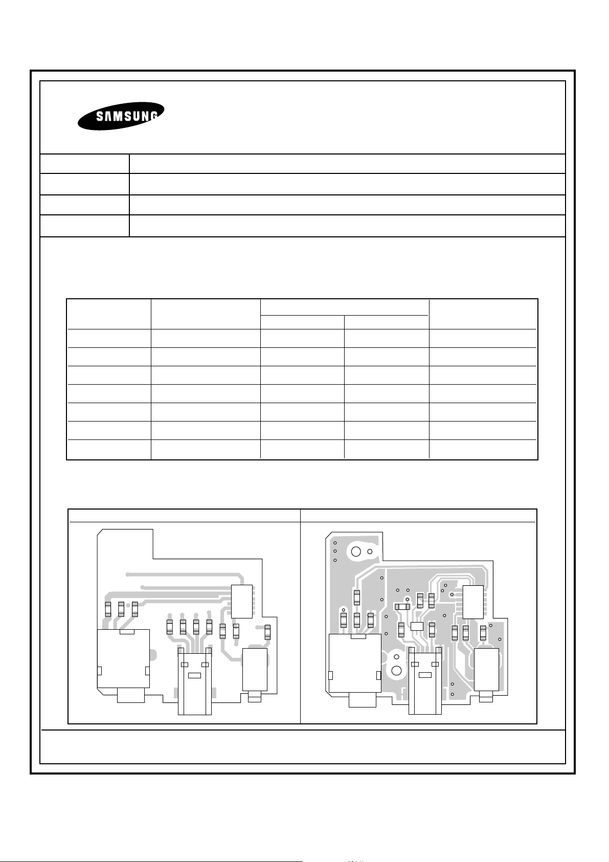
SAMSUNG DIGIMAX 210 SERVICE INFORMATION Jack-Board
We improved some parts on the main pcb ass'y and jack pcb ass'y in order to prevent the
static electricity as follows;
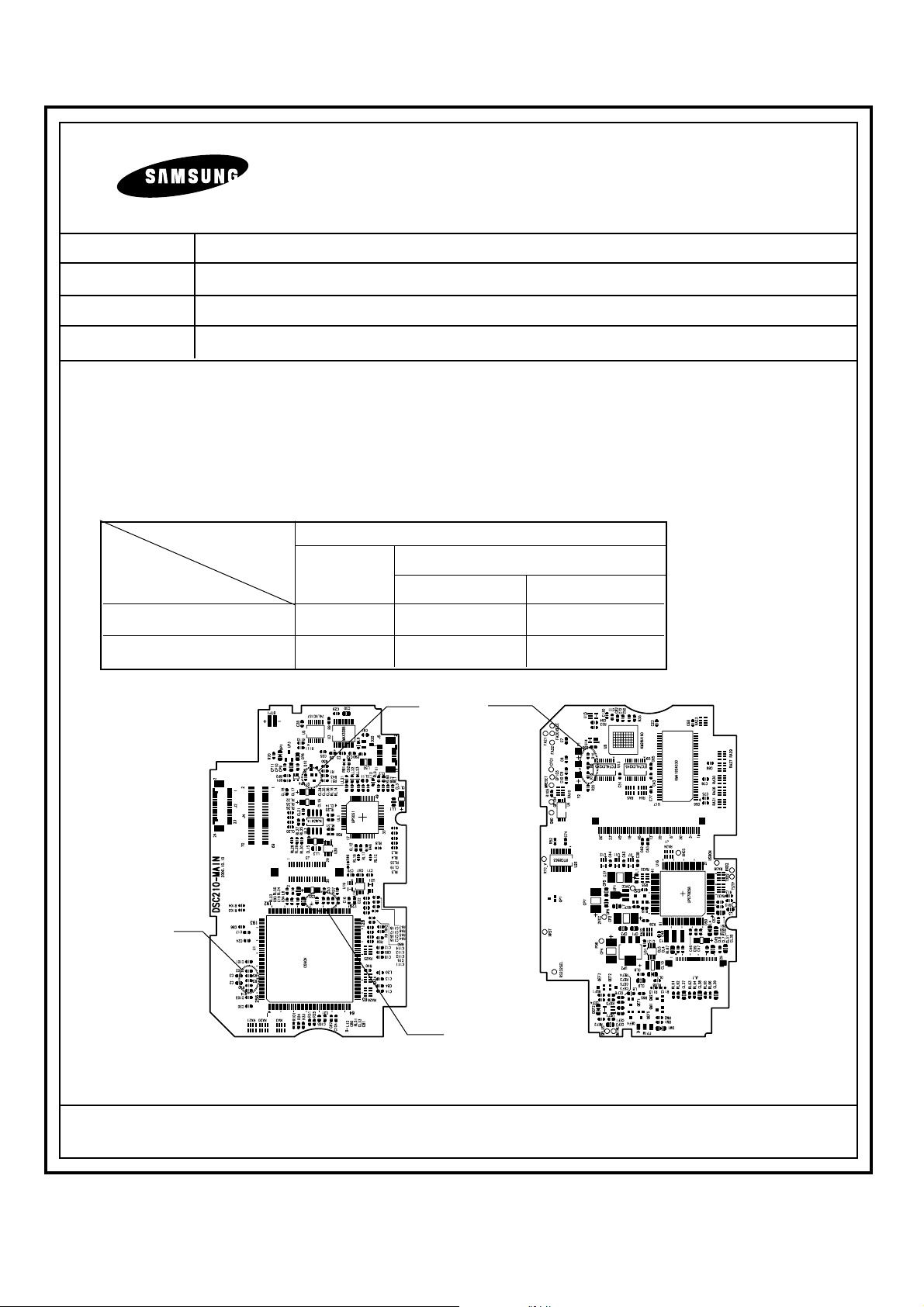
1. Main PCB Ass'y
※ Refer to the next page which parts were located on the Main PCB Ass'y .(Fig. -1)
2. Jack PCB Ass'y
New type
A type B type
L13 ACB1608M040 0Ω 0Ω Top side
R3,R15 27Ω 100Ω 100Ω Top side
R15,R16 100Ω 47Ω 47Ω Bottom side
C80 CL10B104KONC Delete Delete Top side
R2 1.5KΩ 1.5KΩ 0Ω Top side
Q1 UMT3904 UMT3904 UMT2907 Top side
Marking VD55 V55S(M) 55SS Version sticker
Old type
1/2
SERVICE INFORMATION
SAMSUNG TECHWIN CO., LTD.
S/I NO.
DA TE
MODEL
SUBJECT
TECHWIN
200203
February 28, 2002
DIGIMAX 210SE
Improve the Main PCB Ass'y and the Jack PCB Ass'y
Parts Location
Old type New type
11
L8L9L10
J4
L1L2L3
12
J2
1
L4
J1
2
L7
1
L5
L6
4
J3
5
R1
L6L7 L5
L3 L2
L4
U1
L8L1L9
J1
J2
11
12
1
L10
J3
SERVICE INFORMATION
S/I NO.
DA TE
MODEL
SUBJECT
TECHWIN
200203
February 28, 2002
DIGIMAX 210SE
Improve the Main PCB Ass'y and the Jack PCB Ass'y
If you replace the MAIN PCB or JACKPCB with new one, you have to make a pair of two PCB
as below table-A.
If you don
’’
t make a pair of two PCB, some problem occured when downloading the images
form camera to PC.
[Table-A] Compatibility of the Jack PCB Aaa'y withe the Main PCB Ass'y
2/2
SAMSUNG TECHWIN CO., LTD.
Main PCB Ass'y
New type
A type B type
Old type ○○ ×
New type ×× ○
Old type
Main PCB
Ass'y
Jack PCB
Ass'y
[Fig. - 1]
Top side Bottom side
Q1,R2
R15,R16
R3,R5
L13,C80
 Loading...