

Page 1

SERVICE MANUAL
DIGIMAX 202/301
TECHWIN
Page 2

2
CONTENTS
ⅠⅠ
.. SSPPEECCIIFFIICCAATTIIOONN
1. SPECIFICATION ……………………………………………………………………………………………… 4
2. SYSTEM REQUIRMENT ……………………………………………………………………………………… 5
3. TFT LCD PANEL MARK ……………………………………………………………………………………… 6
4. CONNECTION DIAGRAM …………………………………………………………………………………… 8
5. PRODUCT EXTERIOR ………………………………………………………………………………………… 9
ⅡⅡ
.. IINNSSTTAALLLLAATTIIOONN
…………………………………………………………………………………………… 11
ⅢⅢ
.. EEXXPPLLOODDEEDD VVIIEEWW AANNDD PPAARRTTSS LLIISSTT
1. MAIN ASSEMBLY …………………………………………………………………………………………… 16
2. BODY ASSEMBLY …………………………………………………………………………………………… 18
3. FLASH BOARD ASSEMBLY ………………………………………………………………………………… 20
4-1. FRONT COVER ASSEMBLY(D301) ……………………………………………………………………… 22
4-2. FRONT COVER ASSEMBLY(D202) ……………………………………………………………………… 24
5. BACK COVER ASSEMBLY ………………………………………………………………………………… 26
6. PACKING ITEM …………………………………………………………………………………………… 28
7. INITIAL PARTS LIST ………………………………………………………………………………………… 31
ⅣⅣ
.. AADDJJSSUUTTMMEENNTT
1. REPLACEMENT PARTS AND ADJUSTMENT ITEMS ……………………………………………………… 32
2. ADJUSTMENT TOOLS ……………………………………………………………………………………… 32
3. FIRMWARE UPGRADE ……………………………………………………………………………………… 32
4. ADJUSTMENT ITEMS
1) FOCUS ADJUSTMENT …………………………………………………………………………………… 36
2) LCD ADJUSTMENT ……………………………………………………………………………………… 37
5. CHECKING THE CAMERA BEFORE AND AFTER REPAIR ……………………………………………… 38
ⅤⅤ
.. PPRROODDUUCCTTSS CCOONNSSTTRRUUCCTTIIOONN
1. PARTS ARRANGEMENT FOR EACH PCB ASS’Y
1-1) MAIN PCB ASSEMBLY(D301) ……………………………………………………………………… 42
1-2) MAIN PCB ASSEMBLY(D202) ……………………………………………………………………… 44
2) FLASH PCB ASSEMBLY ………………………………………………………………………………… 46
3) KEY PCB ASSEMBLY …………………………………………………………………………………… 48
4) LENS PCB ASSEMBLY ………………………………………………………………………………… 50
Page 3

3
2. CIRCUIT DIAGRAM
1-1) BLOCK DIAGRAM(D301) …………………………………………………………………………… 51
1-2) BLOCK DIAGRAM(D202) …………………………………………………………………………… 52
2) MAIN BOARD TOP VIEW ……………………………………………………………………………… 53
3) SP533 MICRO BGA DSP ……………………………………………………………………………… 54
4) CDS/CCD/DRV…………………………………………………………………………………………… 55
5) ROM/SDRAM/EEPROM/NAND FLASH………………………………………………………………… 56
6) 16 MBYTE NAND FLASH ……………………………………………………………………………… 57
7) SD CARD ………………………………………………………………………………………………… 58
8) MSK1151 TFT INTERFACE……………………………………………………………………………… 59
9) SD/USB/LED/BUZZER…………………………………………………………………………………… 60
10) POWER MODULE ……………………………………………………………………………………… 61
11) POWER SOUR CTRL …………………………………………………………………………………… 62
12) CONNECTOR …………………………………………………………………………………………… 63
13) GPIO FMGPIO DIGTV MAP…………………………………………………………………………… 64
ⅥⅥ.. TTRROOUUBBLLEESSHHOOOOTTIINNGG
1.
PRINCIPAL TROUBLESHOOTING
1) EACH KIND OF ASSEMBLY PROBLEM ……………………………………………………………… 65
2) POWER ON PROBLEM ………………………………………………………………………………… 70
3) APERTURE OPERATION ERROR ……………………………………………………………………… 74
4) IMAGE ERROR…………………………………………………………………………………………… 76
5) ZOOM OPERATION ERROR …………………………………………………………………………… 77
6) BUTTON OPERATION ERROR ………………………………………………………………………… 78
7) STROBO OPERATION ERROR ………………………………………………………………………… 79
8) PROBLEM ABOUT TFT LCD …………………………………………………………………………… 80
2. DISASSEMBLE THE CAMERA ……………………………………………………………………………… 81
Page 4
Ⅰ
. SPECIFICATION
4
11.. CCAAMMEERRAA SSPPEECCIIFFIICCAATTIIOONN
Type D301 : 1/2.7″CCD, D202 : 1/2″CMOS
Image Sensor
Effective Pixels D301 : Approx. 3.2 Mega-pixel, D202 : Approx. 2.0 Mega-pixel
Total Pixels D301 : Approx. 3.3 Mega-pixel, D202 : Approx. 2.1 Mega-pixel
D301 : Lens f= 5.1mm (35mm film equivalent : 33mm)
D202 : Lens f= 9.0mm (35mm film equivalent : 47mm)
F No. D301 : F2.9/F8.0, D202 : F3.5
Still Image mode : 1.0X ~ 3.0X, D202 : 1.0X ~ 2.0X
Digital Zoom Play mode : 1.0X ~ 5.0X, D202 : 1.0X ~ 3.0X
(depends on image size)
Optical Viewfinder
Optical virtual image viewfinder
LCD Monitor 1.6″color TFT LCD
Type Fixed focus with two steps manual adjustment
Focusing Macro : 0.19 ~ 0.21m
Normal : 1.0m ~ infinity
Type Mechanical and Electronic shutter
Speed Normal : 1/4 ~ 1/1000sec. Night : 5 ~ 1/1000sec.(D301)
Control Program AE
Exposure Compensation ±2EV (0.5EV steps)
ISO AUTO
Mode Auto/ Auto&Red-eye reduction/ Fill-in flash / Slow sync/ Flash off
Flash Range Macro : 0.2m, Normal : 1.0 ~ 3.0m(D202 : 1.0 ~ 2.5m)
Recharging Time D301 : Approx. 4 ~ 10sec. D202 : Approx. 8sec.
Effect B&W, Normal, Sepia
Photo Frame 4 frames
White balance Auto/ Daylight/ Cloudy/ Fluorescent/ Tungsten/ Sunset/ Custom
Sharpness Soft/ Normal/ Vivid
Voice recording (Max. 1 hour)
Voice memo in still image(Max. 10sec.)
Size : 320x240
Recording time : memory capacity dependent
Self-timer 10Sec/ 2Sec/ Double Self-timer
Internal Memory : 16MB Flash Memory(D202 : 6MB Flash Memory)
Media External Memory (Not Supplied) : SD Memory Card, Multimedia Card (MMC)
(up to 256MB Guaranteed)
Storage Still image : JPEG(DCF), DPOF Movie clip : AVI(JPEG) Audio : WAV
(D202 - Still image : JPEG(DCF), DPOF Movie clip : AVI)
2048: 2048x1536 Pixels(D301), 1600: 1600x1200 Pixels,
1024: 1024x768 Pixels, 640: 640x480 Pixels
Viewfinder
Lens
Shutter
Voice recording (D301)
Shooting
Focal Length
Range
Movie clip
Image size
File Format
Page 5
5
ⅠⅠ.. SS PP EECC II FF IICCAA TT IIOO NN
22.. SSYYSSTTEEMM RREEQQUUIIRREEMMEENNTTSS
PC with processor better than MMX Pentium 233MHz (XP: Pentium II 300MHz)
Windows 98/98SE/2000/ME/XP
For Windows Minimum 32MB RAM(XP: 128MB)
140MB of available hard-disk space, USB port, CD-ROM drive
800x600 pixels, 16-bit color display compatible monitor
(24-bit color display recommended)
PowerMac G3 or later
Mac OS 9.1~10.2
For Macintosh Minimum 64MB RAM
110MB of available hard-disk space, USB port, CD-ROM drive
QuickTime 4.0 or later (for Movie Clip)
2048: Super fine 12, Fine 24, Normal 36
1600: Super fine 19, Fine 40, Normal 56
1024: Super fine 40, Fine 85, Normal 122
640: Super fine 106, Fine 214, Normal 428
Storage 1600: Super fine 8, Fine 15, Normal 22
1024: Super fine 17, Fine 31, Normal 45
640: Super fine 37, Fine65, Normal 90
*These figures are measured under Samsung’s standard conditions and
may vary depending on shooting conditions and camera settings.
Image Play Single image/ Thumbnails/ Slide show/ Movie Clip
Digital output connector: USB DC power input connector : 3.3V
Video output : NTSC / PAL (user selectable : D301)
Supplied : AA-type alkaline primary batteries
Not Supplied :
Non-rechargeable Battery : AA type - Ni-Mn, Ni-Zn, and Lithium
CR-V3 type - Lithium batteries
Rechargeable Battery : AAtype- Ni-Mh, Ni-Cd(1000mA or above)
CR-V3 type: Digimax Battery I-Pack(SBP-1103)
Battery Pack - Digimax Battery Pack (SBP-3603)
※ Included battery may vary depending on sales region.
Dimensions (WxHxD) 98 x 51 x 38mm
Weight D301 : Approx.122g (without batteries and card), D202 : Approx.120g
Operating Temperature 0 ~ 40 ℃
Operating Humidity 5 ~ 85 %
Camera Driver Storage Driver (Windows98/98SE/2000/ME/XP, Mac OS 9.1~10.2)
Application MGI PhotoSuite, Digimax Viewer
Capacity
(Internal memory)
Interface
Software
D301
(16MB)
D202
(6MB)
Power Source
Page 6
6
ⅠⅠ.. SS PP EECC II FF IICCAA TT IIOO NN
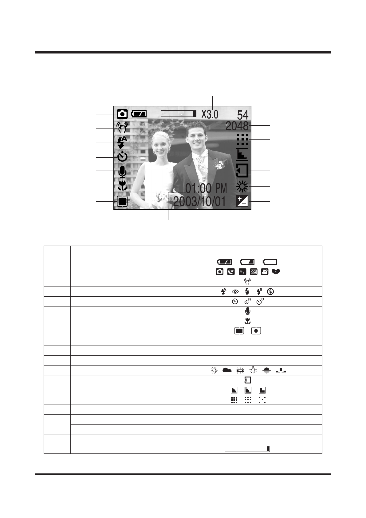
33.. TTFFTT LLCCDD PPAANNEELL MMAARRKK
■ Recording mode
②
⑮
③
④
⑤
⑥
⑭
⑬
⑫
⑪
⑩
⑨
⑦
⑧
⒃
⒔
①
⒖
⒕
[ Image & Full Status ]
No. Description Icons
1 Battery
2 Recording mode
3 Camera shake warning
4 Flash
5 Self-timer
6 Voice memo
7 Macro
8 Metering
9 Time 01:00 PM
10 Date 2003/10/01
11 Exposure compensation -2.0 ~ 0 ~ +2.0 EV
12 White Balance
13 Card Inserted indicator
14 Sharpness
15 Image quality
16 Image size 2048, 1600, 1024, 640
Number of available shots remaining 54
Remaining time( Movie clip/ Voice recording)
02:00/00:05:00
18 Digital Zoom rate X3.0
19 Digital zoom
17
Page 7
7
ⅠⅠ.. SS PP EECC II FF IICCAA TT IIOO NN
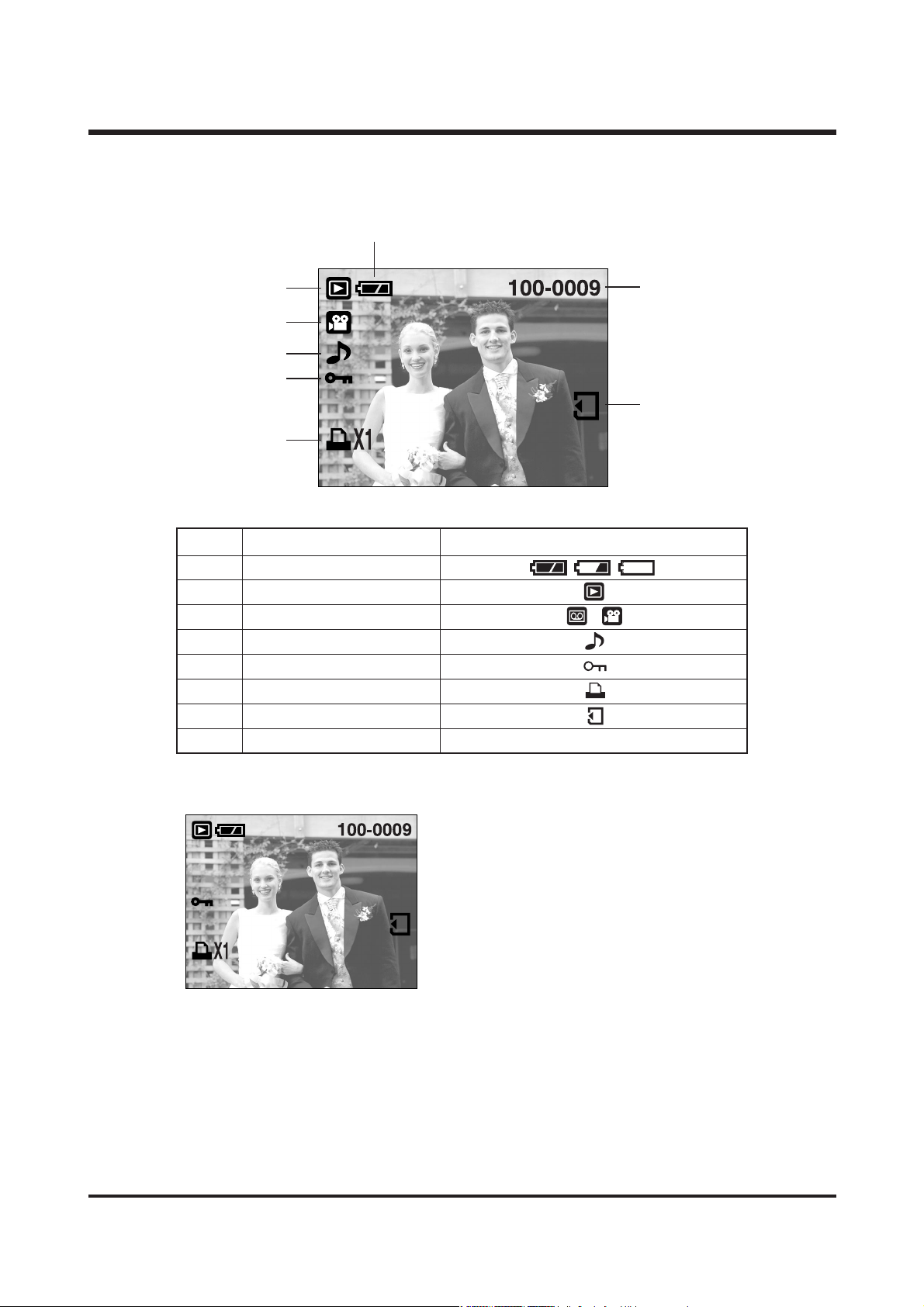
■ Play mode
②
⑥
③
④
⑤
⑧
①
⑦
No. Description Icon
1 Battery
2 Play mode
3 File Type
4 Voice memo
5 Protect indicator
6 DPOF indicator
7 Card Inserted indicator
8 Stored image number 100-0009
SIZE : 1024x768 Size
DATE : 2003/10/01 Recording date
TIME : 17:40:21 Recording time
FLASH : NONE Whether or not the
flash is used.
SIZE : 1024x768
DATE : 2003/10/01
TIME : 17:40:21
FLASH : NONE
Page 8
8
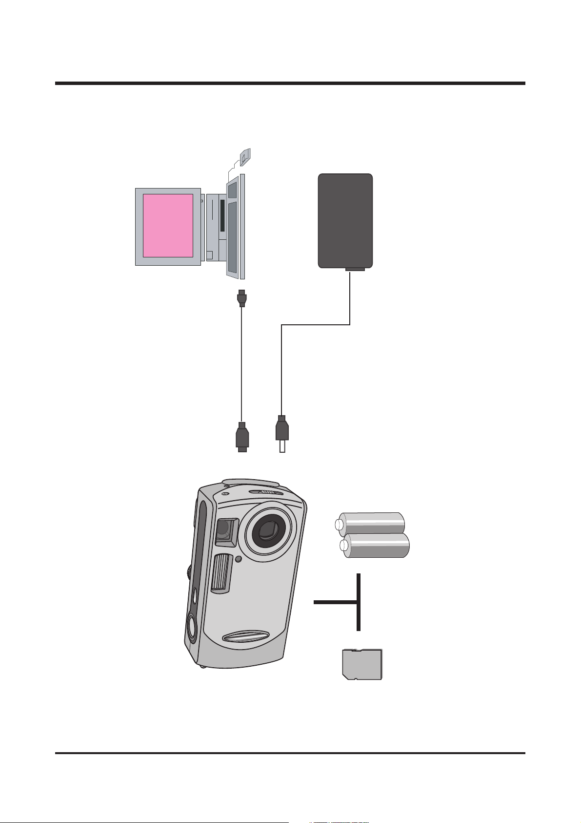
44.. CCOONNNNEECCTTIIOONN DDIIAAGGRRAAMM
ⅠⅠ.. SS PP EECC II FF IICCAA TT IIOO NN
3.3V/ 2.0A
IBM PC / MACINTOSH
USB Cable
Digimax 301/ 202 camera
AC Adaptor
Batteries
Alkarain x2
Card
SD & MMC
Page 9
9
ⅠⅠ.. SS PP EECC II FF IICCAA TT IIOO NN
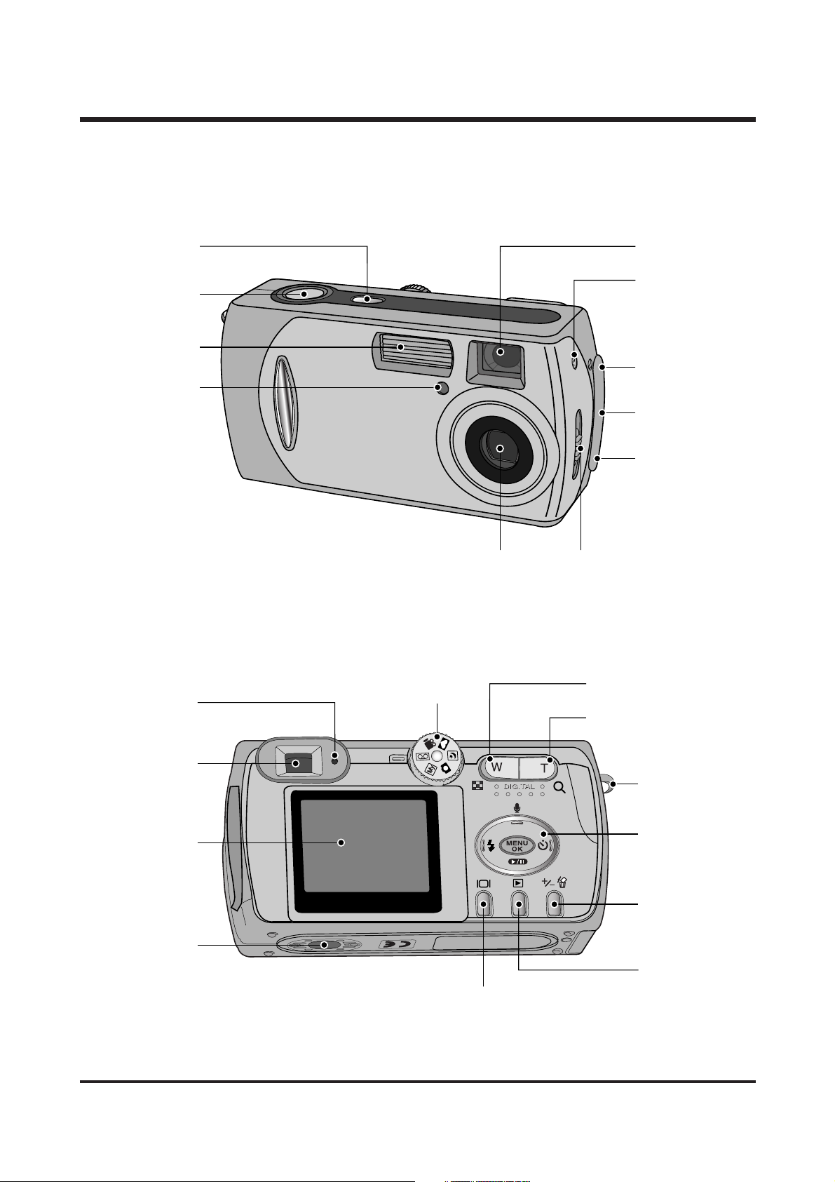
55.. IIDDEENNTTIIFFIICCAATTIIOONN OOFF FFEEAATTUURREESS
Power button
Shutter button
Flash
Self-timer lamp
Camera status
lamp
TELE/Digital zoom button
WIDE/THUMBNAIL button
5-function button
Strap eyelet
Mode dial
LCD button
+&-/ DELETE
button
Play mode button
Viewfinder
LCD monitor
Tripod socket
Viewfinder
Microphone
USB connection
terminal
VIDEO connection
terminal
DC input connection
point
Focus lever
Lens
<<DDii ggiimmaaxx 330011>>
Page 10
10
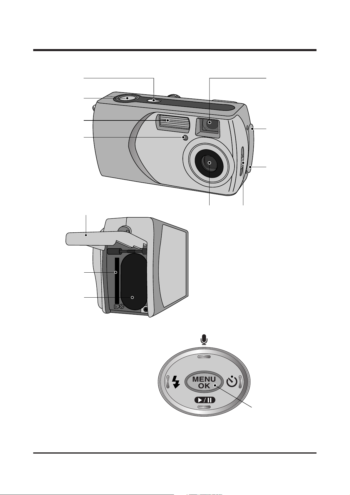
ⅠⅠ.. SS PP EECC II FF IICCAA TT IIOO NN
Memory card slot
Battery chamber
Battery chamber cover
Flash/ LEFT button
Menu/ OK button
Play & Pause/ DOWN button
Self-Timer/ RIGHT button
Voice memo(D301)/ UP button
Power button
Shutter button
Flash
Self-timer lamp
Viewfinder
USB connection
terminal
DC input connection
point
Focus lever
Lens
<<DDii ggiimmaaxx 220022>>
Page 11
11
ⅡⅡ
. INSTALLATION
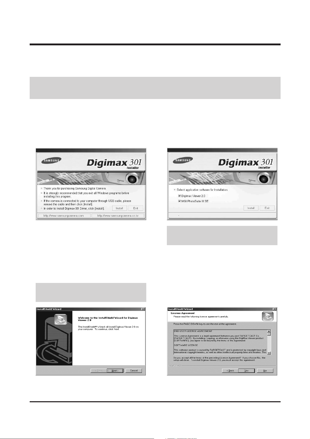
To use this camera with a PC, install the application software first. After this has been done, the stored images
in the camera can be moved to the PC and can be edited by an image editing program.
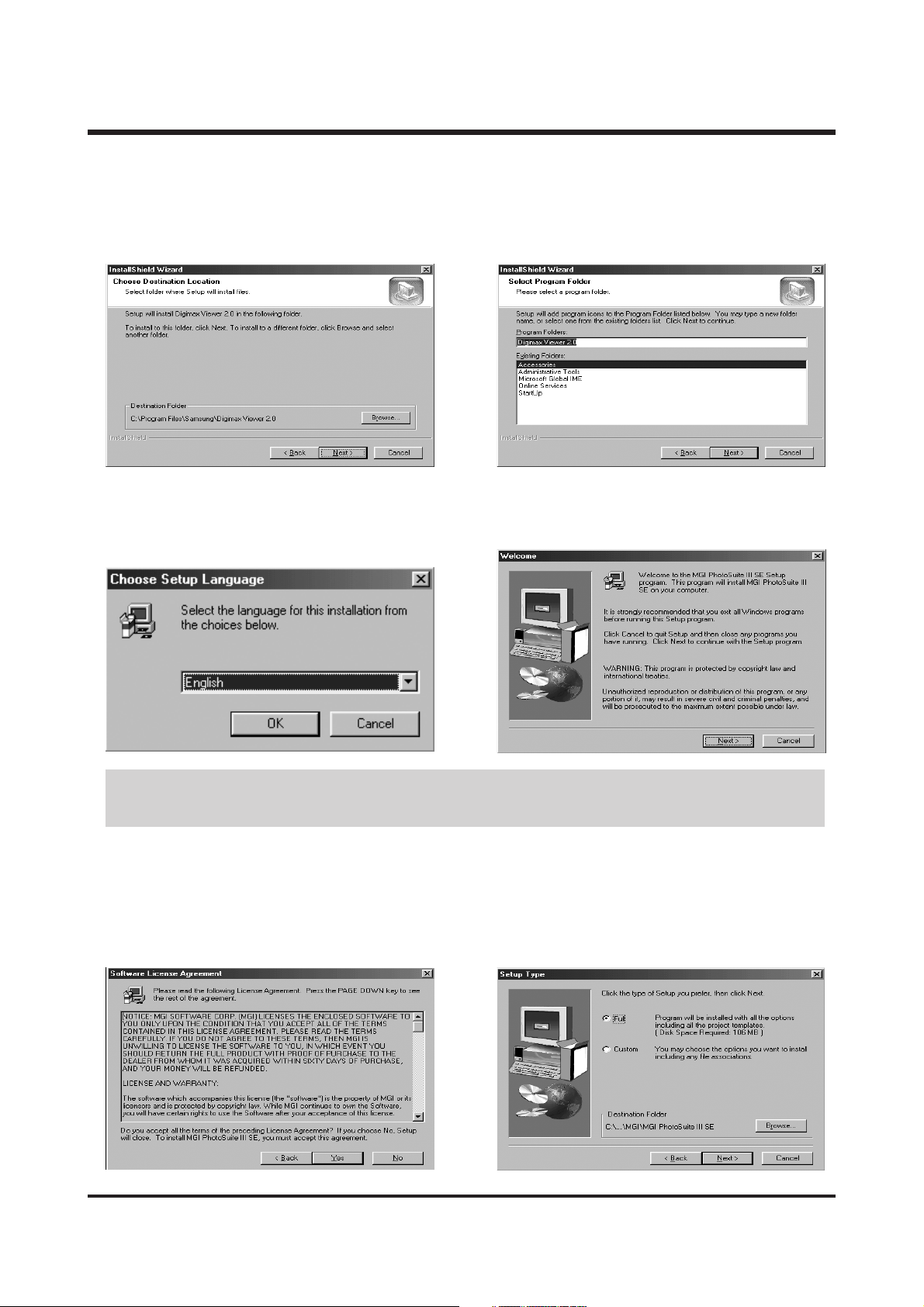
2. Installation is complete. A window for which you
can select application software will be displayed.
Select the application program and click the
[Install] button.
1. Click the [Install] menu in the Autorun frame.
The Digimax 301 camera driver is installed
automatically.
3. Install Digimax Viewer. Click [Next(N) >]. 4. The Software License Agreement window will be
displayed. If you agree to this, click [Yes], the
window will then move to the next step. If you
disagree, click [No] and the installation program
will be canceled.
··
If you select [Cancel] at the step 2, the
application program installation will be cancelled.
··
If you select [Cancel] at step 3, a window for
installing MGI PhotoSuite III SE will be displayed.
● Close other programs before installing the application software.
● Before installing the application software, disconnect the USB connection.
Page 12
12
ⅡⅡ.. II NN SSTTAALLLL AA TTII OO NN
6. A window will open, asking you to choose a folder to
which program icons will be added. Click [Next(N) >].
If you want to add the program icons to a different
folder, choose another folder, and then click [Next >].
5. A destination selection window will open. Click
[Next(N) >]. To copy the files to another folder,
click [Browse (R)..] and choose a folder you want.
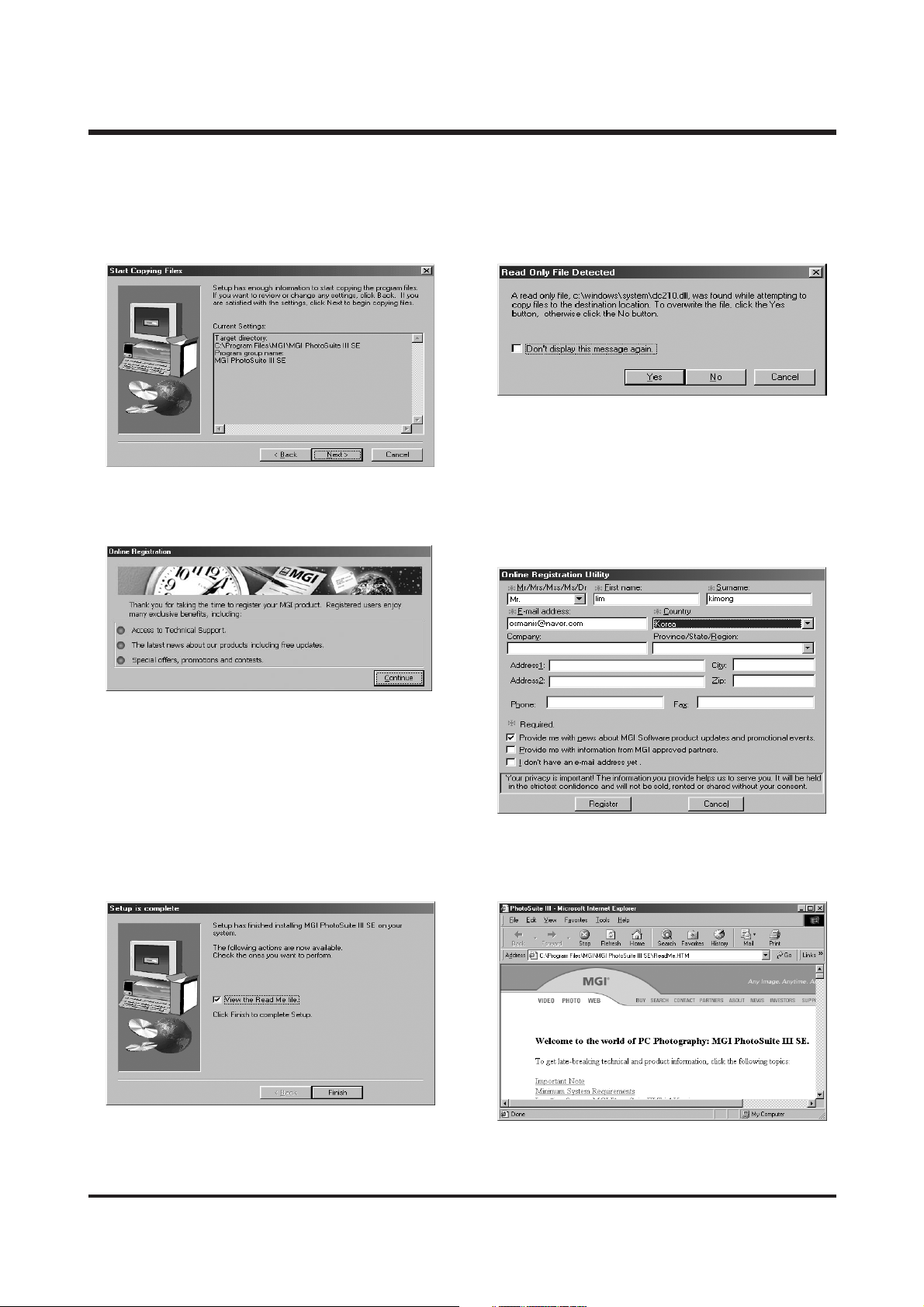
7. Installation is completed.
The [MGI PhotoSuite III SE] installation window will be
displayed as shown alongside. Click the [OK] button.
8. A [Welcome] window will be displayed.
Click the [Next >] button.
9. The Software License Agreement window will be
displayed. If you agree to this, click [Yes], the
window will then move to the next step.
If you disagree, click [No] and the installation
program will be canceled.
10. The [Setup Type] window will appear.
Click [Next(N) >].
[Full] : the program will be installed with all the
options.
[Custom] : you can choose what you would like
to install.
··
If you click [Cancel] in Step 7, the MGI PhotoSuite III SE installation will be canceled and
the Restart Computer window will appear.
Page 13
13
ⅡⅡ.. II NN SSTTAALLLL AA TTII OO NN
* A [Read Only File Dectected] window may be
displayed. Click the [No] button.
* If you click the [Register] button without connecting
to the Internet, an error message will be displayed
on the screen. Click [OK] to proceed to the next
screen.
11. If installation is completed correctly, Autoplay is
registered automatically into the start menu
program as shown below. Click the [Next >]
button.
13. The [Online Registration Utility] window will be
displayed. Fill in the blanks and click the
[Register] button.
12. The MGI Registration window will be displayed.
Click the [Continue] button.
* The MGI III file will open.
Click on the Close button to close the window.
14. MGI PhotoSuite III SE installation is complete.
Click the [Finish] button.
Page 14
14
ⅡⅡ.. II NN SSTTAALLLL AA TTII OO NN
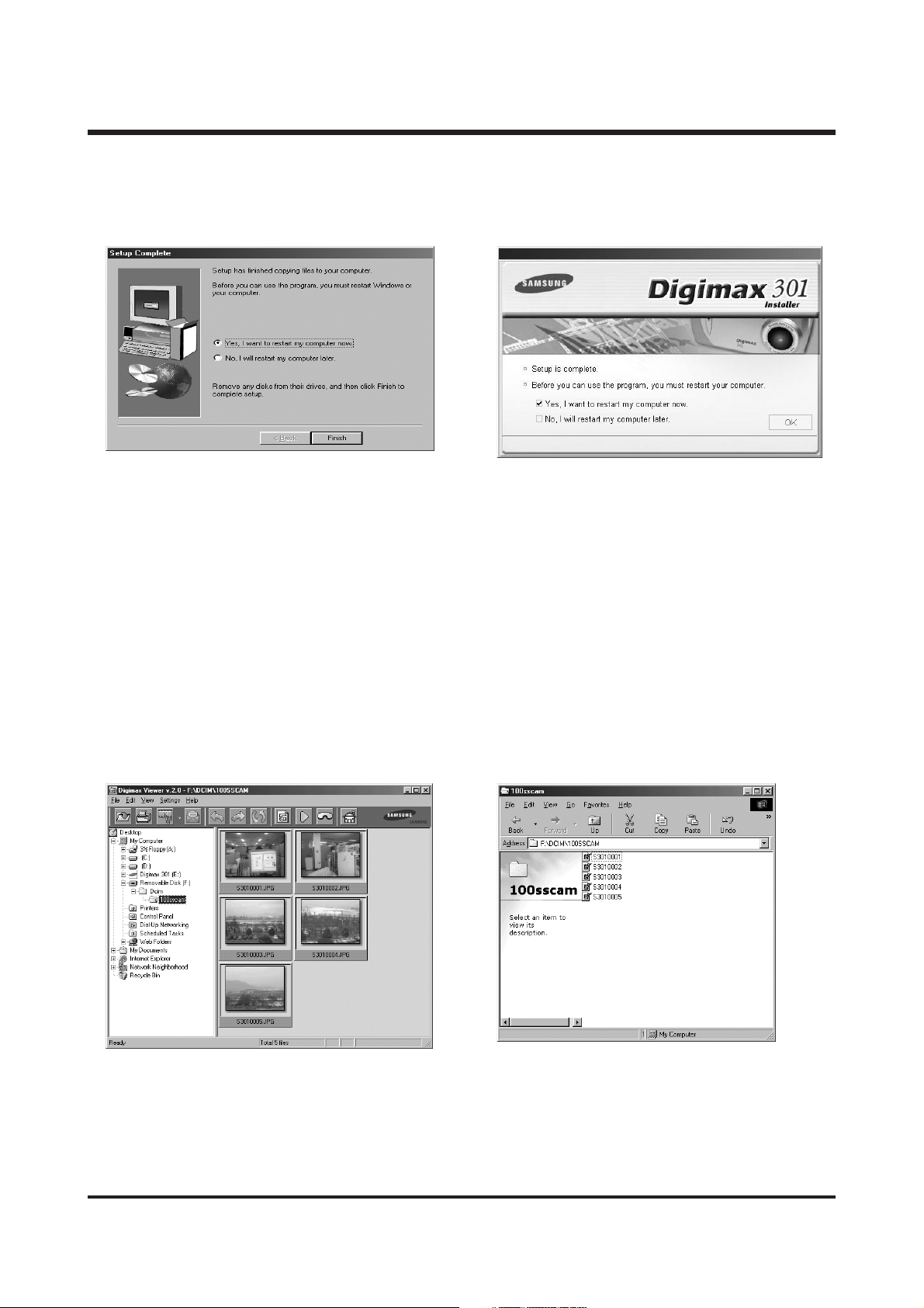
16. To apply changes, you must restart the computer.
Select [Yes, I want to restart my computer now],
and then click [OK].
15. Installation is complete.
Click the [Finish] button.
17. After restarting the computer, connect the PC to the camera with the USB cable.
19. If you can see [Removable Disk] under
[My computer], the camera driver installation
was successful.
Now you can transfer image files from the
camera to PC via the USB cable.
18. Turn the camera power on.
[Found New Hardware Wizard] will open and
the computer will recognize the camera.
※ If you have ever installed an image viewer
program or your OS is Windows XP, an image
viewer program will open. If the image viewer
program opens, the camera driver was setup
successfully.
Page 15
15
ⅡⅡ.. II NN SSTTAALLLL AA TTII OO NN
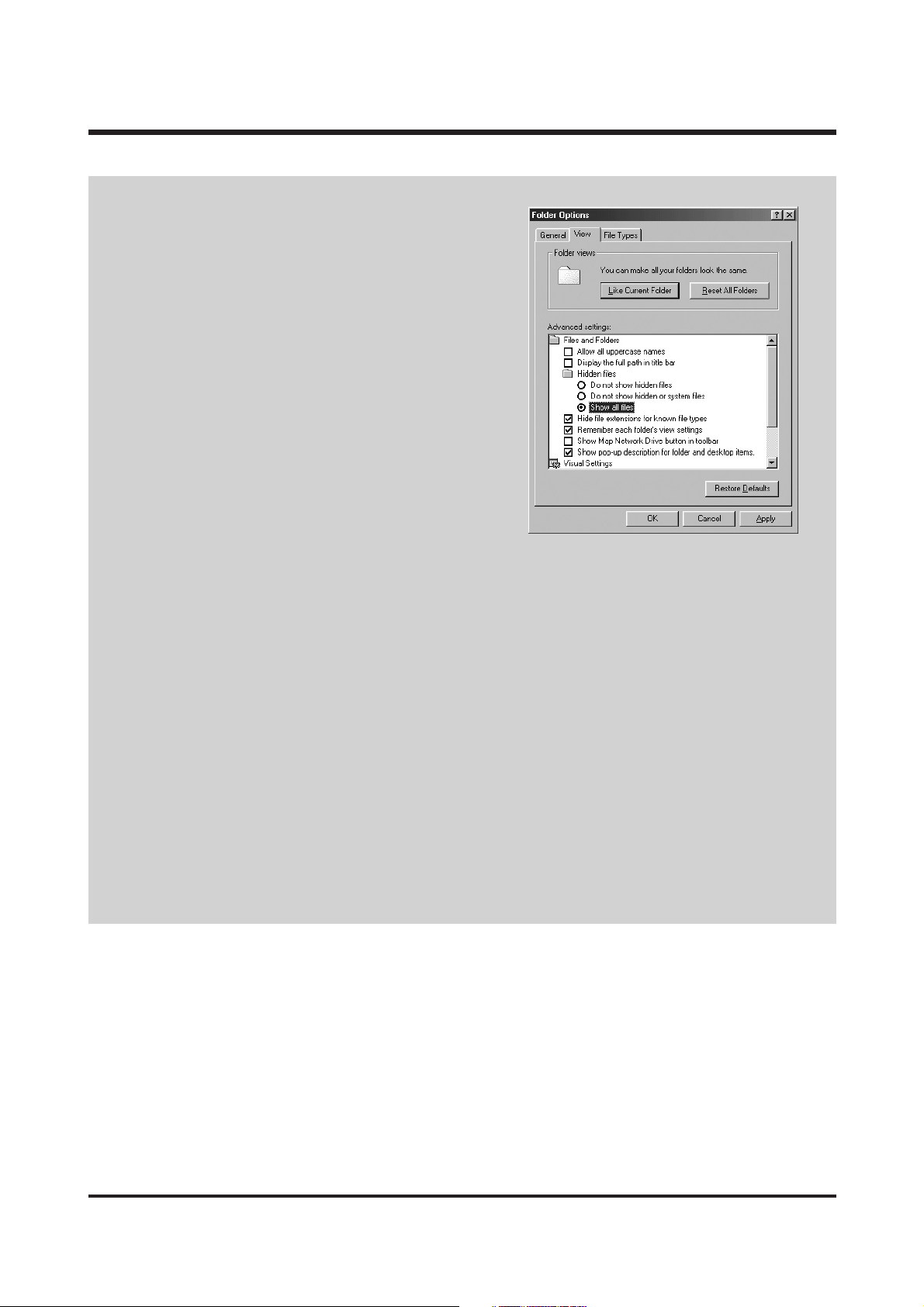
● If you have installed the camera driver,
[Found New Hardware Wizard] may not open.
● After the [Found New Hardware Wizard] window opens,
a window asking you to select a driver file may appear.
In this case, specify the C:\WINDOWS\INF folder
(for Windows 98 and 98 SE).
If you can't find the [INF] folder, check the [Show all files]
button in [Window's Explorer → View → Folder option →
View].
● When connecting the camera to your PC,
it is recommended that you use an AC power adapter.
● Before connecting the camera to the PC, you should first install the camera driver.
● After installing the camera driver, you have to restart your PC.
● If you connect the camera to the PC before installing the camera driver, the [Found New Hardware
Wizard] will open. In this case, cancel the [Found New Hardware Wizard] and disconnect the camera.
Install the camera driver and connect the camera to the PC again.
● Should the computer not find the camera driver after installation, please try one or more of the
following measures.
1. Delete the camera driver, and re-install the driver.
2. Refer to FAQ to check for a possible solution to the problem.
3. If your PC’s central processing unit is VIA chip (This is shown in the USB Host Controller), download
the patch file from the Samsung Camera web page. (http://www.samsungcamera.com)
Page 16
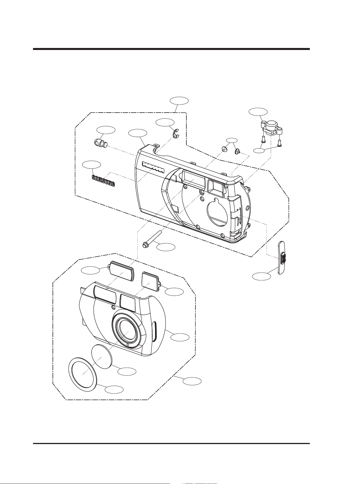
16
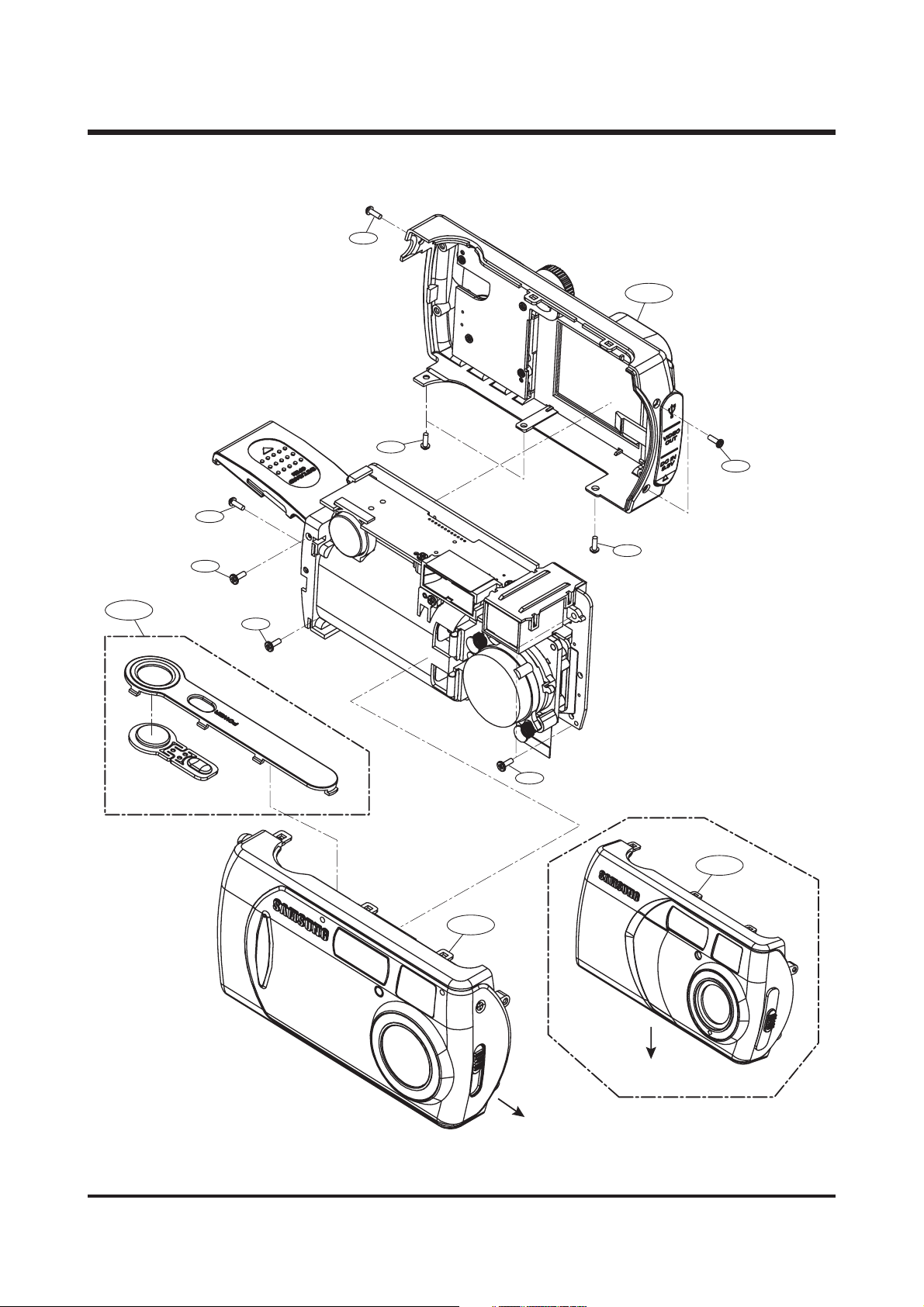
1. MAIN ASSEMBLY
Ⅲ. EXPLODED VIEWS AND PARTS LIST
1-5
1-3
1-5
1-4
1-7
1-6
1-5
1-2
1-8
1-6
1-1
1-1
D202
D301
Page 17

17
ⅢⅢ.. EEXXPPLLOODD EEDD VV IIEEWW SS AA NN DD PP AARRTTSS LLII SS TT
▶▶
PARTS LIST
Fig.No. Parts No. Parts Name Q'ty Remarks
1-1 Q9007198701A FRONT COVER ASS'Y - KENOX DIGIMAX 301 1
Q9007198801A FRONT COVER ASS'Y - DIGIMAX 301 1
Q9007201701A FRONT COVER ASS'Y - KENOX DIGIMAX 202 1
Q9007201801A FRONT COVER ASS'Y - DIGIMAX 202 1
1-2 Q9007198901A TOP COVER ASS'Y - D301 1
Q9007201901A TOP COVER ASS'Y - D202 1
1-3 Q9007199001A BACK COVER ASS'Y - D301 1
Q9007202001A BACK COVER ASS'Y - D202 1
1-4 Q6003041201A SCREW 2
1-5 Q6003041301A SCREW 5
1-6 Q6003041401A SCREW 3
1-7 Q6003041501A SCREW 1
1-8 Q6003041601A SCREW 1
Page 18
18
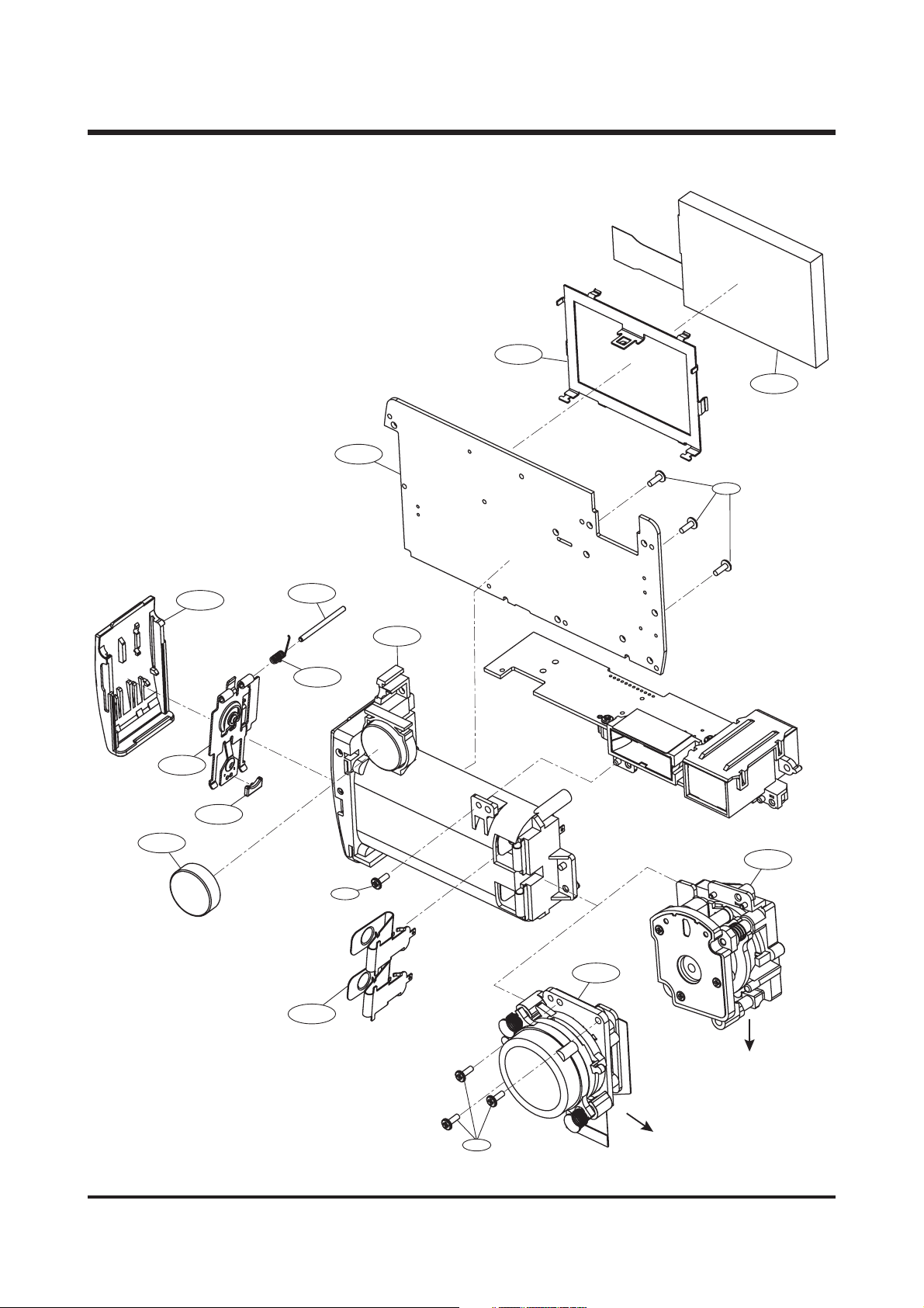
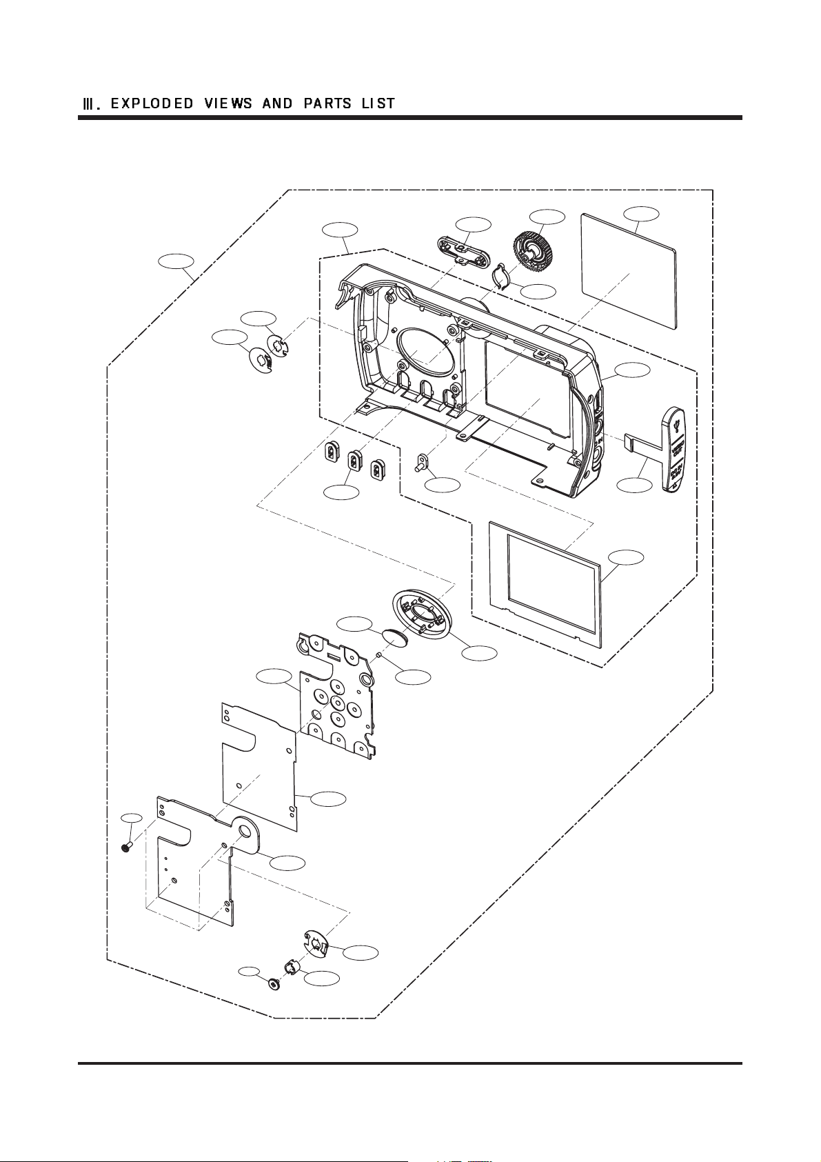
2. BODY ASSEMBLY
ⅢⅢ .. EEXX PPLL OO DDEE DD VV II EEWWSS AA NN DD PP AARR TT SS LL II SSTT
2-11
2-10
2-9
2-13
2-7
2-1
2-8
2-4
2-5
2-3
2-2
2-12
2-13
2-12
2-6
2-13
D202
D301
Page 19

19
▶▶
PARTS LIST
ⅢⅢ.. EEXXPP LL OO DDEE DD VV II EE WW SS AA NN DD PP AARR TT SS LL II SSTT
Fig.No. Parts No. Parts Name Q'ty Remarks
2-1 Q7011046601A BATTERY CONTACT LOWER 1
2-2 Q7211069401A BATTERY STOPPER 1
2-3 Q6107056101A BATTERY COVER SPRING 1
2-4 Q7411103801A BATTERY CONNECTOR AXLE 1
2-5 Q7211069501A BATTERY COMPARTMENT - D301 1
Q7211069801A BATTERY COMPARTMENT - D202 1
2-6 Q7011046701A BATTERY CONTACT UPPER 2
2-7 Q3002001401A PIEZO BUZZER 1
2-8 Q7211069701A BATTERY COVER 1
2-9 Q0704009701A LCD PANEL 1
2-10 Q7211069601A TFT HOLDER 1
2-11 Q9008067101A MAIN BOARD ASS'Y - D301 1
Q9001095701A MAIN BOARD ASS'Y - D202 1
2-12 Q9002123601A LENS ASS'Y - D301 1
2-12 Q9001095801A LENS ASS'Y - D202 1
2-13 Q6003041701A SCREW 7
Page 20
20
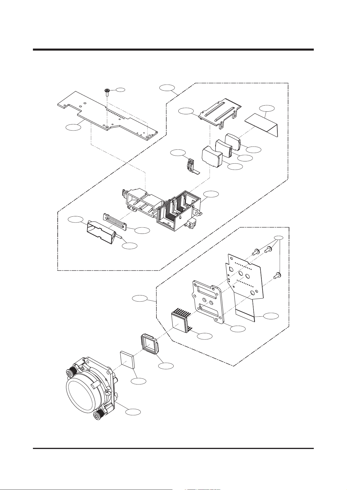
3. FLASH BOARD ASSEMBLY
ⅢⅢ.. EEXXPP LL OO DDEE DD VV II EE WW SS AA NN DD PP AARR TT SS LL II SSTT
3-2
3-10
3-13
3-11
3-9
3-1
3-8
3-7
3-12
3-4
3-5
3-6
3-3
3-21
3-20
3-14
3-15
3-16
3-17
3-18
3-19
Page 21

21
▶▶
PARTS LIST
ⅢⅢ.. EEXXPP LL OO DDEE DD VV II EE WW SS AA NN DD PP AARR TT SS LL II SSTT
Fig.No. Parts No. Parts Name Q'ty Remarks
3-1 Q9003021201A FINDER ASS'Y - D301 1
Q9003021301A FINDER ASS'Y - D202 1
3-2 Q9008067201A ASS'Y M3361-FL DIP 1
3-3 Q7217302401A VF HOLD 1
Q7213034401A VF HOLD 1
3-4 Q6711052201A VF GLASS-2 - D301 1
Q7213034201A VF GLASS-2 - D202 1
3-5 Q6711052301A VF GLASS-3 - D301 1
3-6 Q6711052101A VF GLASS-1 - D301 1
Q7213034301A VF GLASS-1 - D202 1
3-7 Q7217302301A VF HOLD COVER - D301 1
Q7213034501A VF HOLD COVER - D202 1
3-8 Q7014004301A TRIGGER CONTACT 1
3-9 Q7309041401A RUBBER FLASH 1
3-10 Q7014004401A FLASH REFLECTOR 1
3-11 Q0611003501A FLASH TUBER 1
3-12 Q7409152001A FLASH MYLAR 1
3-13 Q6003041801A SCREW 2
3-14 Q9008067301A ASS'Y M3361-LENS SMD PANASONIC - D301 1
3-15 Q9008067401A CCD F PCB ASS'Y - D301 1
3-16 Q7012078501A HEAT SINK FOR CCD - D301 1
3-17 Q0604003001A CCD SENSOR - D301 1
3-18 Q7309041501A CCD RUBBER - D301 1
3-19 Q6735003501A LOW PASS FILTER - D301 1
3-20 Q9002123701A LENS UNIT - D301 1
3-21 Q6003041901A SCREW 3
Page 22
22
ⅢⅢ.. EEXXPP LL OO DDEE DD VV II EE WW SS AA NN DD PP AARR TT SS LL II SSTT
4-1. FRONT COVER ASSEMBLY (D301)
4-19
4-4
4-5
4-3
4-17
4-16
4-15
4-7
4-6
4-9
4-10
4-2
4-18
4-12
4-8
4-11
4-14
4-13
4-1
Page 23

23
ⅢⅢ.. EEXXPP LL OO DDEE DD VV II EE WW SS AA NN DD PP AARR TT SS LL II SSTT
▶▶
PARTS LIST
Fig.No. Parts No. Parts Name Q'ty Remarks
4-1 Q9007199401A
DECORATION COVER ASS'Y-KENOX DIGIMAX 301
1 D301
Q9007199401A
DECORATION COVER ASS'Y-DIGIMAX 301
1 D301
4-2 Q7217302501A LED GUIDE FRONT 1
4-3 Q7217302601A TRIPOD BASE 1
4-4 Q7411103901A MASTER STRAP HOLE 1
4-5 Q7017040101A E-RING 1
4-6 Q7217302701A ASS'Y FRONT COVER 1 D301
4-7 Q7217302801A FLASH ACRYL 1
4-8 Q7217302901A FRONT VF COVER 1
4-9 Q0902008101A MICROPHONE 1
4-10 Q7217303001A MIC HOLDER 1
4-11 Q7217303101A
ASS'Y DECORATION COVER-KENOX DIGIMAX 301
1 D301
Q7217303101A
ASS'Y DECORATION COVER-DIGIMAX 301
1 D301
4-12 Q7217303201A LENS FOCUS BUTTON 1 D301
4-13 Q7217303301A LENS COVER 1
4-14 Q7217303401A LENS PLATE 1 D301
4-15 Q7217303501A LOGO PLATE 1
4-16 Q7217303601A ASS'Y HAND HOLD 1
4-17 Q6003042001A SCREW 1
4-18 Q6003042101A SCREW 6
4-19 Q9007199301A INNER FRONT COVER ASS'Y 1 D301
Page 24
24
ⅢⅢ.. EEXXPP LL OO DDEE DD VV II EE WW SS AA NN DD PP AARR TT SS LL II SSTT
4-2. FRONT COVER ASSEMBLY (D202)
4-4
4-13
4-6
4-16
4-3
4-5
4-14
4-15
4-7
4-2
4-10
4-8
4-9
4-11
4-1
4-12
Page 25

25
ⅢⅢ.. EEXXPP LL OO DDEE DD VV II EE WW SS AA NN DD PP AARR TT SS LL II SSTT
▶▶
PARTS LIST
Fig.No. Parts No. Parts Name Q'ty Remarks
4-1 Q9007204401A
DECORATION COVER ASS'Y-DIGIMAX 202
1 D202
Q9007205001A
DECORATION COVER ASS'Y-KENOX DIGIMAX 202 1
D202
4-2 Q7217302501A LED GUIDE FRONT 1
4-3 Q7217302601A TRIPOD BASE 1
4-4 Q7411103901A MASTER STRAP HOLE 1
4-5 Q7017040101A E-RING 1
4-6 Q9007205101A ASS'Y FRONT COVER 1 D202
4-7 Q7217302801A FLASH ACRYL 1
4-8 Q7217302901A FRONT VF COVER 1
4-9 Q7217307701A
ASS'Y DECORATION COVER-DIGIMAX 202
1 D202
Q7217314801A
ASS'Y DECORATION COVER-KENOX DIGIMAX 202 1
D202
4-10 Q7217307801A LENS FOCUS BUTTON 1 D202
4-11 Q7217303301A LENS COVER 1
4-12 Q7217307901A LENS PLATE 1 D202
4-13 Q7217303501A LOGO PLATE 1
4-14 Q6003042001A SCREW 1
4-15 Q6003042101A SCREW 6
4-16 Q9007204501A INNER FRONT COVER ASS'Y 1 D202
Page 26
26
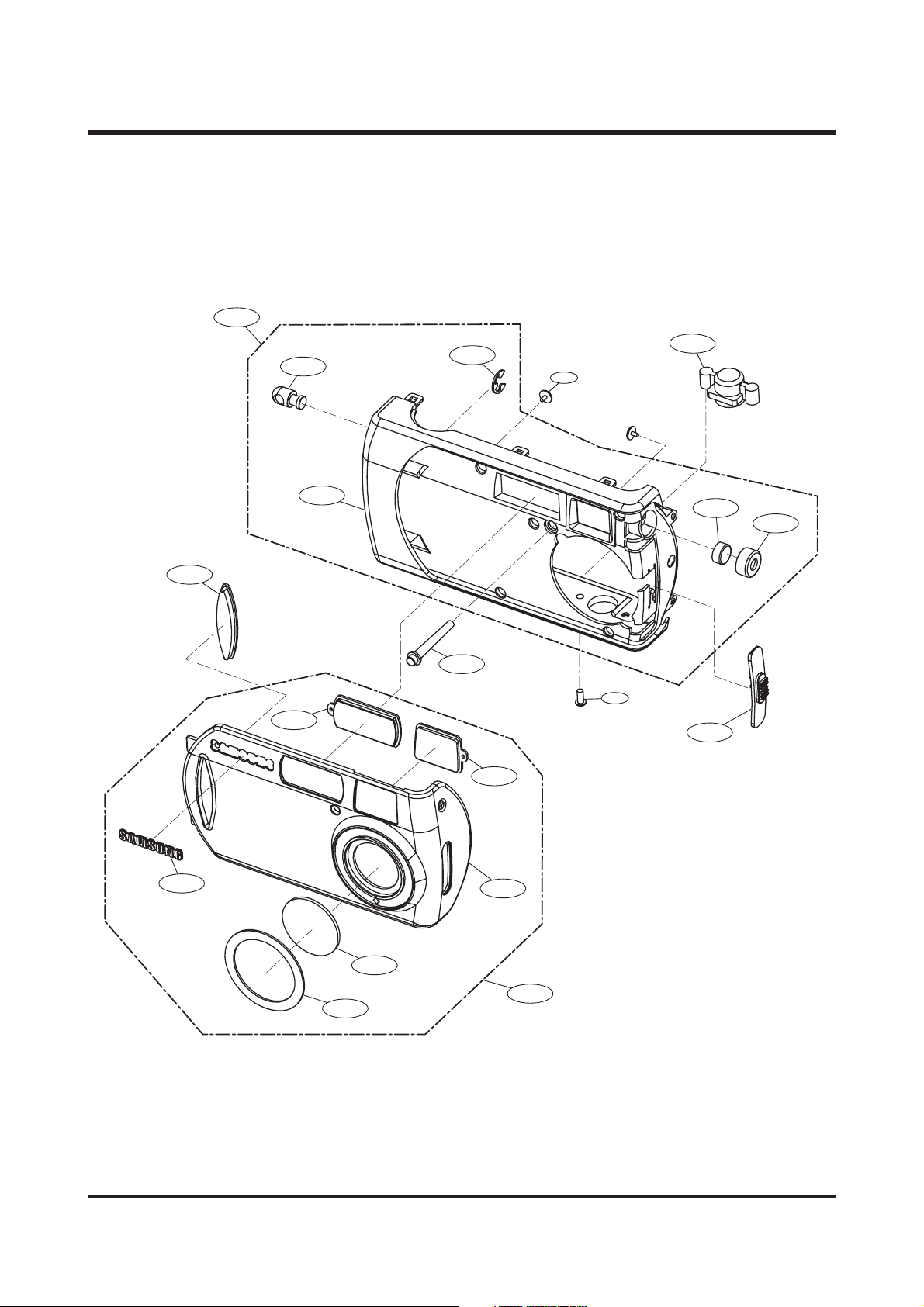
5. BACK COVER ASSEMBLY
5-1
5-11
5-10
5-23
5-9
5-8
5-4
5-3
5-2
5-6
5-5
5-7
5-14
5-22
5-21
5-16
5-13
5-12
5-15
5-17
5-18
5-19
5-20
Page 27

27
PARTS LIST
Fig.No. Parts No. Parts Name Q'ty Remarks
5-1 Q9007199601A BACK COVER ASS'Y - D301 1
Q9007202001A BACK COVER ASS'Y - D202 1
Q9007209801A BACK COVER ASS'Y - D401 1
5-2 Q7217303701A ASS'Y MODE DIAL - D301 1
Q7217308001A ASS'Y MODE DIAL - D202 1
Q7217317401A ASS'Y MODE DIAL - D401 1
5-3 Q7017040201A MODE DIAL SPRING 1
5-4 Q7217303801A ASS'Y ZOOM BUTTON 1
5-5 Q7217303901A ASS'Y BACK COVER 1
5-6 Q7217304001A TFT COVER 1
5-7 Q7309041601A JACK COVER - D301/401 1
Q7309042201A JACK COVER - D202 1
5-8 Q7217304101A LED GUIDE BACK 1
5-9 Q7217304201A ASS'Y BUTTON 1
5-10 Q7017040301A MODE DIAL WASHER 1
5-11 Q7017040401A MODE DIAL CONTACT 1
5-12 Q7217304301A ASS'Y DIRECTION BUTTON 1
5-13 Q7217304401A ASS'Y OK BUTTON 3
5-14 Q7409152101A TFT SPONGE 1
5-15 Q7409152201A OK BUTTON SUPPORT 1
5-16 Q7309041701A KEYPAD RUBBER A 1
5-17 Q7309041801A METAL DOME 1
5-18 Q9007199501A ASS'Y KEY SMD 1
5-19 Q7017040501A MODE DIAL CONTACT REVERSE 1
5-20 Q7411104001A MODE DIAL SPACE RING 1
5-21 Q6003042201A SCREW 4
5-22 Q6003042301A SCREW 1
5-23 Q9007199701A BACK COVER SUB ASS'Y- D301 1
Q9007209901A BACK COVER SUB ASS'Y- D401 1
Q9007202101A BACK COVER SUB ASS'Y- D202 1
Page 28

28
6. PACKING ITEM
ⅢⅢ.. EEXXPP LL OO DDEE DD VV II EE WW SS AA NN DD PP AARR TT SS LL II SSTT
6-14 6-15 6-16
6-9
6-20
6-19
6-1
6-10
6-17
6-11
6-12
6-13
6-18
6-3
6-4
6-7
6-6
6-5
6-8
6-2
Page 29

29
▶▶
PARTS LIST
ⅢⅢ.. EEXXPP LL OO DDEE DD VV II EE WW SS AA NN DD PP AARR TT SS LL II SSTT
Fig.No. Parts No. Parts Name Q'ty Remarks
6-1 QP960210101A PE BAG (FOR CAMERA) 1
6-2 Q6909011601A PE BAG (FOR ACCESSORY) 1
6-3 Q6901172401A INNER PAD_D1/D301/D202_EXP 1
6-4 Q6904025201A POUCH_D301/D202 1
6-5 Q6806170401A Q/GUIDE_KENOX D301_KOR 1
Q6806170501A Q/GUIDE_D301_ENG 1
Q6806170601A Q/GUIDE_D301_GER 1
Q6806170701A Q/GUIDE_D301_FRA 1
Q6806170801A Q/GUIDE_D301_SPA 1
Q6806170901A Q/GUIDE_D301_ITA 1
Q6806171001A Q/GUIDE_D301_CHI(T) 1
Q6806171101A Q/GUIDE_D301_DUT 1
Q6806171201A Q/GUIDE_D301_POR 1
Q6806171301A Q/GUIDE_D301_SWE 1
Q6806171401A Q/GUIDE_D301_DEN 1
Q6806171501A Q/GUIDE_D301_FIN 1
Q6806171601A Q/GUIDE_D301_RUS 1
Q6806171701A Q/GUIDE_D301_CHI(S) 1
Q6806173201A Q/GUIDE_KENOX D202_KOR 1
Q6806173301A Q/GUIDE_D202_ENG 1
Q6806173401A Q/GUIDE_D202_GER 1
Q6806173501A Q/GUIDE_D202_FRA 1
Q6806173601A Q/GUIDE_D202_SPA 1
Q6806173701A Q/GUIDE_D202_ITA 1
Q6806173801A Q/GUIDE_D202_CHI(T) 1
Q6806173901A Q/GUIDE_D202_DUT 1
Q6806174001A Q/GUIDE_D202_POR 1
Q6806174101A Q/GUIDE_D202_SWE 1
Q6806174201A Q/GUIDE_D202_DEN 1
Q6806174301A Q/GUIDE_D202_FIN 1
Q6806174401A Q/GUIDE_D202_RUS 1
Q6806174501A Q/GUIDE_D202_CHI(S) 1
6-6 Q6806171801A U/MANUAL_KENOX D301_KOR 1
Q6806171901A U/MANUAL_D301_ENG 1
Q6806172001A U/MANUAL_D301_GER 1
Q6806172101A U/MANUAL_D301_FRA 1
Q6806172201A U/MANUAL_D301_SPA 1
Q6806172301A U/MANUAL_D301_ITA 1
Q6806172401A U/MANUAL_D301_CHI(T) 1
Q6806172501A U/MANUAL_D301_DUT 1
Q6806172601A U/MANUAL_D301_POR 1
Q6806172701A U/MANUAL_D301_SWE 1
Q6806172801A U/MANUAL_D301_DEN 1
Q6806172901A U/MANUAL_D301_FIN 1
Q6806173001A U/MANUAL_D301_RUS 1
Q6806173101A U/MANUAL_D301_CHI(S) 1
Q6806174601A U/MANUAL_KENOX D202_KOR 1
Q6806174701A U/MANUAL_D202_ENG 1
Q6806174801A U/MANUAL_D202_GER 1
Page 30

30
ⅢⅢ.. EEXXPP LL OO DDEE DD VV II EE WW SS AA NN DD PP AARR TT SS LL II SSTT
Fig.No. Parts No. Parts Name Q'ty Remarks
Q6806174901A U/MANUAL_D202_FRA 1
Q6806175001A U/MANUAL_D202_SPA 1
Q6806175101A U/MANUAL_D202_ITA 1
Q6806175201A U/MANUAL_D202_CHI(T) 1
Q6806175301A U/MANUAL_D202_DUT 1
Q6806175401A U/MANUAL_D202_POR 1
Q6806175501A U/MANUAL_D202_SWE 1
Q6806175601A U/MANUAL_D202_DEN 1
Q6806175701A U/MANUAL_D202_FIN 1
Q6806175801A U/MANUAL_D202_RUS 1
Q6806175901A U/MANUAL_D202_CHI(S) 1
6-7 Q6807002601E WARRANTY CARD_KOREA 1
Q6807003003R WARRANTY CARD_EXP 1
Q6807003802D WARRANTY CARD_UK 1
Q6807010902B WARRANTY CARD_RUS(3 YEARS) 1
Q6807011301B WARRANTY CARD_TSOE(CHINA) 1
Q6807009502D CARD_PRODUCT MEXICO 1
6-8 Q6901183301A G/T BOX_KENOX D301_KOR 1
Q6901183401A G/T BOX_D301_EXP/AUS 1
Q6901183501A G/T BOX_D301_USA/CAN 1
Q6901183601A G/T BOX_KENOX D202_KOR 1
Q6901183701A G/T BOX_D202_EXP/AUS 1
Q6901183801A G/T BOX_D202_USA/CAN 1
6-9 Q4301001801A "ALKALINE (1.5V, AA) 2EA - DURACEL ULTRA" 1
6-10 Q4308000201A LI-ION BATTERY SBP-1103(CR-V3 Li-ion Type) 1
6-11 Q4309001001A LI-ION & NI-MH CHARGER SBC-1103MH 1
6-12 Q3719002501A AC ADAPTOR_SBP-1103(I-PACK) 1
6-13 Q3801003001A AC CODE CABLE_KOR-D1 1
Q3801003201A AC CODE CABLE_EXP-D1 1
Q3801003101A AC CODE CABLE_USA-D1 1
Q3801001001A AC CODE CABLE_UK-DSC220SE 1
Q3801003401A AC CODE CABLE_AUS-D1 1
6-14 Q7409121701A WRIST STRAP_D 201/D300/D301/D202 1
6-15 Q3801002801A USB CABLE_D200/201/300/301/202 1
6-16 Q3802002501A VIDEO CABLE_D 301 1
6-17 Q4602000501A SECURE DIGITAL CARD(32MB) 1
6-18 Q4609005801A DRIVER + MGI PHOTOSUITE (E/F/G/S/I/DUT/P) 1
Q4609005901A DRIVER + MGI PHOTOSUITE (E/JPN/T.C/S.C/KOR) 1
Q4609006001A DRIVER + MGI PHOTOSUITE (E/F/G/S/I/DUT/P) 1
Q4609006101A DRIVER + MGI PHOTOSUITE (E/JPN/T.C/S.C/KOR) 1
6-19 Q7409149101A FCC LABEL_D301_EXP (MADE IN CHINA) 1
Q7409149201A FCC LABEL_D301_EXP (MADE BY SAMSUNG) 1
Q7409149301A MIC LABEL_KENOX D301_KOR (MADE IN CHINA) 1
Q7409149401A FCC LABEL_D202_EXP (MADE IN CHINA) 1
Q7409149501A FCC LABEL_D202_EXP (MADE BY SAMSUNG) 1
Q7409149601A MIC LABEL_KENOX D202_KOR (MADE IN CHINA) 1
6-20 Q6804050801A PRODUCT STICKER_D301 1
Q6804050901A PRODUCT STICKER_DIGIMAX 301_MEXICO 1
Q6804051201A PRODUCT STICKER_D202 1
Q6804051301A PRODUCT STICKER_DIGIMAX 202_MEXICO 1
Page 31

PAGE PARTS NO. PARTS NAME SPEC SYMBOL
21 Q0611003501A FLASH TUBER
19 Q0704009701A LCD PANEL
23 Q0902008101A MICROPHONE
19 Q3002001401A PIEZO BUZZER
21 Q6735003501A LOW PASS FILTER-DSC301
19 Q7011046601A BATTERY CONTACT LOWER
19 Q7011046701A BATTERY CONTACT UPPER
27 Q7017040201A MODE DIAL SPRING
27 Q7017040401A MODE DIAL CONTACT
19 Q7211069501A BATTERY COMPARTMENT-DSC301
19 Q7211069701A BATTERY COVER
17 Q7217302101A ASSY TOP COVER-DSC301
23 Q7217302501A LED GUIDE FRONT
25 Q7217302601A TRIPOD BASE
25 Q7217302801A FLASH ACRYL
23 Q7217302901A FRONT VF COVER
23 Q7217303301A LENS COVER-DSC301
27 Q7217303701A ASSY MODE DIAL-DSC301
27 Q7217304001A TFT COVER
21 Q7309041501A CCD RUBBER-DSC301
27 Q7309041601A JACK COVER-DSC301
27 Q9007199501A KEY SMD ASSY
19 Q9008067101A MAIN BOARD ASSY-DSC301
17 Q9007198701A FRONT COVER ASS'Y-KENOX DIGIMAX 301
17 Q9007198801A FRONT COVER ASS'Y-DIGIMAX 301
17 Q9007198901A TOP COVER ASS'Y
17 Q9007199001A BACK COVER ASS'Y
27 Q9007199701A BACK COVER SUB ASS'Y
23 Q9007199401A DECORATION COVER ASS'Y-KENOX DIGIMAX 301
23 Q9007199401A DECORATION COVER ASS'Y-DIGIMAX 301
25 Q9007204401A DECORATION COVER ASS'Y-DIGIMAX 202
25 Q9007205001A DECORATION COVER ASS'Y-KENOX DIGIMAX 202
25 Q7217307801A LENS FOCUS BUTTON-DSC 202
25 Q7217307901A LENS PLATE-DSC 202
27 Q7217308001A ASS'Y MODE DIAL-DSC 202
27 Q7309042201A JACK COVER-DSC 202
17 Q9007201701A FRONT COVER ASS'Y-KENOX DIGIMAX 202
17 Q9007201801A FRONT COVER ASS'Y-DIGIMAX 202
17 Q9007201901A TOP COVER ASS'Y-DSC 202
27 Q9007202001A BACK COVER ASS'Y-DSC 202
27 Q9007202101A BACK COVER SUB ASS'Y-DSC 202
19 Q9001095701A MAIN BOARD ASS'Y-DSC 202
19 Q9001095801A LENS ASS'Y-DSC 202
19 Q7211069801A BATTERY COMPARTMENT-DSC 202
31
7. INITIAL PARTS LIST
ⅢⅢ .. EE XX PP LL OO DD EE DD VV II EE WW SS AA NN DD PP AA RR TT SS LL II SS TT
Page 32

32
Ⅳ. ADJUSTMENT
11.. RREEPPLLAACCEEMMEENNTT PPAARRTTSS AANNDD AADDJJUUSSTTMMEENNTT IITTEEMMSS
Digimax 301 requires electrical adjustments when certain parts are replaced.
The table below indicates the adjustments required for the respective part replacements.
22.. AADDJJUUSSTTMMEENNTT TTOOOOLLSS
▶ Equipment
- Osiloscope, Photo sensor AMP
▶ Chart
- Focus chart : Please contact to our website(www.ssa.net) and print the focus Chart on the
A3 size paper from the “201CHART.pdf”
33.. FFIIRRMMWWAARREE UUPPGGRRAADDEE
❶❶ DDoowwnnll oo aa dd tthhee ff iirr mmww aarree
1. Contact to our web site(www.ssa.net) and go to the Digital Driver menu.
2. Click the No. 44 and you can get the latest firmware as below.
3. Download the file “MEGAD301.BIN”to the [Removavle Disk].
Main Board Flash Board Key board Shutter Board TFT LCD Lens Unit
Focus ● ●
LCD ● ●
❶ Position the mouse cursor over the
dd oo ww nn lloo aa dd ll iinn kk
(above) and click
the right mouse button.
Select
SS aavvee tt aarr gg ee tt AA ss.... ..
Page 33

33
4. The file [MEGAD301.BIN] will be downloaded to the [Removable Disk].
FF iirrmmwwaarree UUpp ggrraa ddee
1. Insert the SD card into the camera.
ⅣⅣ.. AADDJJUUSS TTMM EENNTT
❷ Choose the [Removable Disk].
Change the file name to
MEGAD301.BIN,
Click the save button.
❸ It will be download
automatically
❹
The file [MEGAD301.BIN] will be
downloaded to the [Removable Disk].
Page 34

34
ⅣⅣ.. AADDJJUUSS TTMM EENNTT
2. Insert SD card and turn on the power, pressing wide button.
The firmware will be upgraded automatically after the beep if you turn on the power.
※※ AA nnyy ppooss iitt iioonn ooff mmoodd ee dd iiaall iiss OOKK..
3. The process of firmware upgrade is like below.
① WRITE NAND ② CHECKING ③ ERASE MEMORY
④ UPDATE ⑤ ROM CHECK ⑥ DRAM CHECK
If the ROM data accords with DRAM data, the camera will be on as soon as off automatically
after the beep.
※※ II ff tt hhee RR OO MM dd aatt aa ddooeess nn'' tt aacc ccoo rr dd wwiitthh DDRRAA MM ddaattaa,, ttrryy tt oo uuppgg rraadd ee aa ggaa iinn ..
Page 35

35
ⅣⅣ.. AADDJJUUSS TTMM EENNTT
CC hheecc kkiinngg FFiirrmm wwaarree VVeerrssii oo nn
This is the way how to check firmware version.
1. Take out SD card from the camera.
2. If you turn on the power, pressing
LCD button, the camera will get into
the test mode.
※※ AA nnyy ppooss iitt iioonn ooff mmoo ddee ddiiaall iiss OO KK..
3. The warning message will be displayed when getting into
the test mode.
4. Press the right direction key(Self timer) to get into the
test mode.
Press the down direction key(Recording/Play-back) in
test mode to get into 4th item.
- 4 TEST ROMCODE is to check firmware version.
5. Press the right direction key(Self timer) to check
firmware version.
TThh ee ffiirrmm wwaarree vveerrssii oonn ii ss 33001144 ..
6. Turn off the power if you want to get out of the test mode.
Page 36

36
ⅣⅣ.. AADDJJUUSS TTMM EENNTT
44.. AADDJJUUSSTTMMEENNTT IITTEEMMSS
1) FOCUS adjustment
a. Contact to our website(www.ssa.net)
b. Arrange the camera shown as below.
※ AF Chart : www.ssa.net
201CHART.PDF
c. Select the normal focus mode by switching the focus lever and turn on the camera.
d. Zoom in upto 2X and point the center of TFT LCD toward the center of the chart.
e. Rotate the lens until you get a fine image.
f. After finishing the adjustment, glue two parts of the lens to be fixed.
g. After fixing the Lens(wait about 5 minutes), take images in Normal, Portrait and Macro focus
mode order. Download the images and check the focus.
※ Download the chart from the website and put it on 5 places as below.
2.3m
AF Chart
Tripod
Camera
6
5
6
4
5
4
3
3
2
2
2
2
3
3
4
4
6
5
6
4
5
4
3
3
2
2
2
2
3
3
4
4
6
5
6
4
5
4
3
3
2
2
2
2
3
3
4
4
6
5
6
4
5
4
3
3
2
2
2
2
3
3
4
4
6
5
6
4
5
4
3
3
2
2
2
2
3
3
4
4
Page 37

37
ⅣⅣ.. AADDJJUUSS TTMM EENNTT
2) LCD adjustment
▶ Equipment
- Osiloscope, Photo sensor AMP
a. Connect the Photo sensor AMP to the Oscilloscope.
b. Select No 14, TEST COLORBAR, from the TESTMODE MENU.@(Figure 1)
c. Select Black & White bar image (Figure 2)
[Figure 1] [Figure 2]
d. Put the Photo sensor on the LCD monitor and rotate the VR1 until the lowest frequency displayed
on the osiloscope is selected.
e. After finishing the adjustment, glue the VR1.
TESTMODE MENU
14 TEST COLORBAR
2002/12/06 16:11:39
UP/DOWN/RIGHT
Page 38

38
ⅣⅣ.. AADDJJUUSS TTMM EENNTT
55.. CCHHEECCKKIINNGG TTHHEE CCAAMMEERRAA BBEEFFOORREE AANNDD AAFFTTEERR RREEPPAAIIRR
Check the camera before and after repair to find bad items or camera malfunction.
●● HHooww tt oo ss eell eecctt tthhee TTEESSTT MMOODDEE
a. Turn on the camera with pressing the LCD button and the TESE MODE will be selected shown
as below.
b. Press the right button and No.1 item of TEST MODE will be displayed as shown below.
Press the right button and items will be displayed in order.
c. TEST MODE items
d. Press the MENU button or turn off the camera and the TEST MODE menu will disappear.
WARRING!!
FOR FACTORY USE
PRESS MENU KEY TO QUIT
RIGHT KEY TO ENTER
TESTMODE MENU
1 TEST FOCUS
2002/12/06 16:11:39
UP/DOWN/RIGHT
TEST MODE item
UP/DOWN : change theTEST MODE item
RIGHT : selecting the TEST MODE item
TEST MODE TEST MODE items Remarks
1 FOCUS
2 MSCALIB
3 BURN IN
4 ROMCODE
5 STROBE
6 EEPROM
7 SOLENOID
8 BUZZER
9 LIFE TEST
10 CARD
11 NAND
12 SDRAM
13 BATTERY
14 COLORBAR
15 KBD
Page 39

39
ⅣⅣ.. AADDJJUUSS TTMM EENNTT
1) Checking the FOCUS
a. When the TEST FOCUS(Figure 1) is selected, press the right button and Figure 2 will be displayed
to indicate focus values of each position.
Focus area is divided into 5 positions, value displayed upper LCD monitor indicates center focus
value and others indicate focus value of each position.
b.
Exposure Value(EV) displayed the bottom center of the LCD monitor indicates current exposure value.
c. When the figure 2 is displayed, press the right button again and figure 3 will display to indicate
focus values of around the camera and center area.
[Figure 1] [Figure 2] [Figure 3]
d. Focus positions are like below.
Each value on the figure 2 and figure 3 indicate each of focus value
from ① to ⑤.
The higher value means the better focus.
2) TEST MSCALIB
a. Put the camera on the AE TESTER.
b. Set the AE TESTER to LV 17.
c. Select No. 2 of the TEST MODE and press the right button. After checking the shutter speed,
value(Figure 2) will be displayed. If the speed value is 25~35, it functions well but if not, you
must change the lens unit as it's inferior lens unit.
[Figure 1] [Figure 2]
TESTMODE MENU
1 TEST FOCUS
2002/12/06 16:11:39
UP/DOWN/RIGHT
45
108 ┼ ┼ 110
105 ┼ ┼ 115
EV 0.72
45
3
108 110
45
105 115
①②
③
④⑤
TESTMODE MENU
2 TEST MSCALIB
2002/12/06 16:11:39
UP/DOWN/RIGHT
2 TEST MSCALIB
VALUE : 33
ANY KEY EXIT
Shutter speed value :
25~33
Page 40

40
ⅣⅣ.. AADDJJUUSS TTMM EENNTT
3) TEST BURNING
Checking the camera function and quality.
▶ During the first 30 minutes, check the camera functions in order shown as below.
Flash charging and firing→ Checking the EEPROM→ Checking the NAND→ Checking the SDRAM→
Check the flash charging, Aperture and shutter at the same time(If it fails, “NG”message will
display.)
▶ During the last 30 minutes, check the camera functions in order shown as below.
Changing the image size→ Changing the quality→ Flash on/off→ Recording a movie clip(of each
recording time)→ Operating menus after taking a picture(DELETE ONE, DEL ALL, FORMAT, etc.)
4) TEST ROMCODE
You can check the version of the firmware.
a. Select No.4 of the TEST MODE and press the right button. The version of the firmware will display
as shown below.
5) TEST STROBE
This menu is used for checking flash charging and firing. It's done as followings.
- REDY PIN CHECK : When the finish is fully charged, “STROBO IS READY”message will display,
If not, “STROBO NOT READY”message will display.
- CHARGE STROBE : Press the right button and the flash charging will start.
- TRIGGER : Press the right button and the flash will fire.
- TRIGGER ONCE : Press the right button and the flash will fire again.
- TRIGGER LOOP : Press the right button and the flash will fire in succession.
6) TEST EEPROM EEPROM.
Checking the EEPROM status.
Press the right button and the DATA stored in the EEPROM for checking is read to check whether
it operates well or not.
7) TEST SOLENOID
Checking the Aperture and Shutter status.
- AP+MS O/C : Making the aperture and shutter turn on and off continuously at the same time.
- MSHUTTER OPEN : Shutter OPEN
- MSHUTTER CLOSE : Shutter CLOSE
4 TEST ROMCODE
VERSION : SF2-2021
DATE : 2002/11/01
CHECKSUM : 7E12 H
CHECKSUM(BOOT) : 92C7 H
ANY KEY EXIT
Main board version : 20
Firmware version : 21
After upgrading the firmware, check whether the
CHECKSUM value is correct or not.
·Firmware ver. : 2021
·CHECKSUM : 7E12 H
Page 41

41
ⅣⅣ.. AADDJJUUSS TTMM EENNTT
- APERTURE OPEN : Aperture OPEN
- APERTURE CLOSE : Aperture CLOSE
- MSHUTTER O/C : Making the shutter turn on and off continuously.
- APERTURE O/C : Making the aperture turn on and off continuously.
8) TEST BUZZER
You can check the buzzer status, type, ON, ERROR and OFF.
9) LIFE TEST
Item for checking the camera status and it check the items related with recording menu only and
check them just 1 time. It differ from the BURNIN items.
You can check IMAGE SIZE, IMAGE QUALITY, STROBO ON/OFF, etc. in this item.
10) TEST CARD
Item for recognition of SD card. After inserting a SD card, select TEST item and “CARD INSERTED”
message will display. If the card didn't insert, “NO CARD”message will display.
11) TEST NAND
Item for displaying contents of the internal memory and deleting all contents.
12) TEST SDRAM
Checking the SDRAM.
13) TEST BATTERY
Item for checking the battery icon displaying. Connect the POWER SUPPLY to the camera and
check the icons.
The FULL icon must be displayed in 3V, LOW in 2.2V and EMPTY in 2.0V.
14) TEST COLOR BAR
Item for checking the TFT LCD color status. There are 9 kinds of color sub item.
1. VERTICAL COLOR BAR 2. BLACK & WHITE BAR 3. RED 4. GREEN 5. BLUE
6. BLACK 7. WHITE 8. HORIZONTAL COLOR BAR 9. COLOR display test
15) TEST KEBD KEY
Item for checking the button operation status.
Page 42

42
1. PARTS ARRANGEMENT FOR EACH PCB ASS'Y
1-1) MAIN PCB Assembly (D301)
a) Parts Arrangement
<TOP>
Ⅴ. PRODUCT CONSTRUCTION
MIC Part
Couldn't Power On
Component N.G
Power Part
Flash Memory
C117
C255
MIC1
R214
L2009304
2003-10-03
R205
R225
R218
R206
R213
C137
2
R233
C149
MA REV: 3.0
-
(L11-L13,Y1,Q13,U12)
M3361
PAN
1
JP1
11
48
12
U12
1
C132 R204
C140
R224
R279
C91
C254
R234 R226
C142
L11
Q8
B1
R187
R220
R227
R130
R184
R229
C150 C151
R235
C94
R178
C133
C147
R180
R182
LED1
R210
R209
R215
R207
R221
R239
D5
C143
R258
C95
Q7
BUZ1
R144
R88
C90
R82
R92
B3
R188
C126
T1
11
SD1
12
C124
B5
Q5
R198
C144
R216
R241
R143
C32
R5
C38
C119
R4
C186
R245
L13
L12
C26
R1
R3
C35
R277
C188
1
8
10
RP2
R242
8
R2
R6
R7
R9
C40
C39
C34
C36
R110
R100
R95
B8
C185
U28
R244
C166
Q15
R240
R237
R275
R276
R278
R273
C127
R14R13
L4
L2
C160
C162
Q13
Q18
R137
RPC23
C184
R274
R202
C130
L9
RP1
C83
C84
C167
C89
C128
C131
1
C62
1
27
R138
R173
RPC21
B6
C57
R250
RP3
R189
R190
C173
48
C63
R58
RPC3
R197
BAT2
C43
R257
RPC14 RPC17
R111
B7
C44
U2
U5
U10
R256
RPC4
C56
R105
RPC11
R70
L8
C252
37
24
R139
RPC19
R63
B10
C64
C253
RPC15
L5
C66
25
RPC12
R140
C169
D10
C65
C51
C58
54
R251
RPC18
R15
BAT1
2
C87
28
R254
RPC13
RPC6 RPC5
RPC9 RPC8
FPC1
Q1
C85
C112
C107
R169
R200
R196R194
R199
C123
C118
R183
R97
R25
Q2
C111
C37
1
R171
R170
C108
R191
V30
-
MA
-
R175
C116
R174
13
MINTON M3361
VSP 1021 Controller
Top Overlay
SDRAM
Dsp Parts
Page 43

43
<BOTTOM>
ⅤⅤ.. PP RR OO DD UU CCTT CC OO NN SSTTRR UU CCTTII OONN
Couldn't Power On
Component N.G
Download Defect
R83
C97
48
U14
Nand Flash
1
R64
R134
R135
C96
R142
J3
RTC
C135
D4
Power part
R232
R219
C139
R212
R217
C148
R222
C141
Q6
(U23,D6,Q14,Q16,Y1,U21)
LED2
C136
R203
C146
U23
C154
USB Part
Component N.G
(B3.B11.B12.USB CON1)
B13
B14
R141
C134
R208
C153C152
Q9
R211
Q10
C138
C157
C158
C155
Y1
B2
C93
R185
C121
L10
C20
Q11
C163
C164
R223
R230
R228
D6
B11
R176
Y2
C33
R8
R179
C19
R181
C145
Q17
C156
D8
D7
C120
B12
R186
USB_CON1
D9
Q16
R238
C159
R231
Q12
RPC22
GC1
R236
R177
C125
RPC20
C16
L14
C99
C161
Q14
C49
C187
C25
C14
R11
R10
R243
C168
C50
Q4
RPC2
C15
C1
D1
J5
R148
1
U4
JP2
C24
C11
C8
C165
R145
C105
C52
R20
J1
C41
U16
C88
U6
9
10
C4
C28
RPC1
C86
R152
C59
C60
C45
C5
C17
R16
T
R
C18
L1
C12
C170
C98
C106
R18
C61
C79
2
C22
C171
R168
C101
R12
1
R73
C6
C27
RPC16
Q19
R247
D3
C100
R146
U18
R17
C67
C46
C42
C80
C9
C7
R154
R159
C54
R19
C68
C47
C31
C21
C102
1
C72
C29
C13
C10
C23
2
R158
R21
C69
C48
J2
RPC7
R57
R246
D11
C103
C104
VR1
C55
C53
C75
1
C92
C30
C2
C3
R253
R252
C172
L3
J4
RPC10
R50
R79
R255
R80
R201
TFT1
C174
R28
C129
C78
C76
C73
C70
U13
C122
C114
R52
C81
U8
B9
G
U21
C113
D2
L6
R112
R192
R195
U7
R248
C115
R54
RPC25
C110
R172
C74
C82
L7
R22
RPC24
R193
C109
33
C71
8
R249
C175
Bottom Overlay
V30
-
MA
-
MINTON M3361
TFT LCD Controller
TFT LCD Defect
image Black
(U18,U61,LENS,TFT1)
EEPROM
Power off automatically
Component N.G(D1,GC1)
image Defect
(U6,U3,U18,TFT1,Lens)
Page 44

44
1-2) MAIN PCB Assembly (D202)
a) Parts Arrangement
<TOP>
ⅤⅤ.. PP RR OO DD UU CCTT CC OO NN SSTTRR UU CCTTII OONN
Page 45

45
<BOTTOM>
ⅤⅤ.. PP RR OO DD UU CCTT CC OO NN SSTTRR UU CCTTII OONN
Page 46

46
2) FLASH PCB Assembly
a) Parts Arrangement
<TOP>
ⅤⅤ.. PP RR OO DD UU CCTT CC OO NN SSTTRR UU CCTTII OONN
Couldn't Strobe
Connect N.G (JP1)
Component N.G
(U1,U2,B3,Q2,D1,L1)
Couldn't Charge
Connect N.G (JP1)
Component N.G
(U1,Q2,B1,B2)
Couldn't Power ON
Connect N.G (JP1)
Component N.G
(S1)
BATT
BATT
PWR_SW
CHARGE
D5U
READY
SW_COL1
TRIGGER
SW_COL3
SW_COL2
AGND
AGND
Q2
G
C5
S1
D3
L1
Q1
D1
FLASH Parts
R10
C6
C1
R6
R11
U2
B3
D4
FLASH V3.0
-
L2009402
M3361
2003/10/1
R2
C9
B2
R8
R1
R7
U1
R12
SW1
B1
R9
C8
Top Overlay
R5
C10
Page 47

47
<BOTTOM>
ⅤⅤ.. PP RR OO DD UU CCTT CC OO NN SSTTRR UU CCTTII OONN
Couldn't Strobe
Connect N.G (JP1)
Component N.G
(R3,C7,T2)
Couldn't Charge
Connect N.G (JP1)
Component N.G
(T1)
T2
R4
C7
R3
1
T1
FLASH Parts
C2
Bottom Overlay
JP1
Page 48

48
3) KEY PCB Assembly
a) Parts Arrangement
<TOP>
ⅤⅤ.. PP RR OO DD UU CCTT CC OO NN SSTTRR UU CCTTII OONN
Key Defect
Metal Mode Set N.G
SW1
M3361 KEY V3.0
L2009503
2003/10/3
SW7
SW9
SW8
SW4
SW5
SW3
SW2
SW10
SW6
D301 KEY BOARD V3.0 Top Overlay
Page 49

49
ⅤⅤ.. PP RR OO DD UU CCTT CC OO NN SSTTRR UU CCTTII OONN
<BOTTOM>
Key Defect
Connect N.G (JP1)
Component N.G
(Q1,R5)
1
JP1
TP8
D1
1
D2
1
D301 KEY BOARD V3.0 Bottom Overlay
Page 50

50
ⅤⅤ.. PP RR OO DD UU CCTT CC OO NN SSTTRR UU CCTTII OONN
4) LENS PCB Assembly
a) Parts Arrangement
<TOP>
JP2
Image Black
Component N.G
(Q1,R5)
C7
C6
R1
C3
C1
D1
D2
IR6
C5
IR3
C8
R2
C2
R5
C4
R4
JP1
Q1
26 FPC1
1
Page 51

51
ⅤⅤ.. PP RR OO DD UU CCTT CC OO NN SSTTRR UU CCTTII OONN
2. CIRCUIT DIAGRAM
1-1) BLOCK DIAGRAM (D301)
Right
5.0V
BAT
STROBO BOARD
VIDEO
3.3V
EEPROM
USB
Power SW
Shutter SW
OUT
93C66
V1.1
KEY BOARD
3.3V
2.5V
Zin Zout
up
ok
down
Left
RTC
SPCA533
BGA 288
DSP
LCD PlayBack EXP/DEL
3.3V
8MBit
29LV800
Flash ROM
3.3V
3.3V
15V
CASIO
TFT LCD
16M BYTE
NAND Flash
SD/MMC CARD
A5V
1.6 Inch
8 16 32 64 128
256MB
V DRIVER
AN20101A
PANASONIC
3.3V
-8.0V
CCD
PANASONIC
3.3V
12.0V
Fix
Focus
Image
ADC
MN39480
3.0V
-8.0V
LENS
Shutter
VAP-1021
3.3V
A3.0V
IRIS
Moter
Driver
WT1076B
5.0V
AAx2 3V
MIX
BAT
CR-V3
POWER
MODULE
3.3V
ADAPTER
3.3V
AT1382A
8Mx 16
SDRAM
Page 52

52
ⅤⅤ.. PP RR OO DD UU CCTT CC OO NN SSTTRR UU CCTTII OONN
1-2) BLOCK DIAGRAM (D202)
&
MODE DIAL
D5V BATTD3V3
KEY BOARD
SHUTTER, POWER S/W
AND STROBE MODULE BOARD
93C66
EEPROM
D3V3
D2V5
V1.1
USB
D3V3
Real Time Colock Crystal
MI - 2000
CMOS SENSOR
82K 768Hz
DSP
SPCA533
SHUTTER
27MHz
DRIVE
WT7010
D3V3
D3V3
AA x 23V
BATT
8M Bit
29LV800
FLASHROM
SDRAM
8M x 16
POWER
MODULE
AT1382A
D3V3
D3V3
8, 16, 32
64, 128MB
SDMMC CARD
8M Byte
NAND FLASH
TFT
CASIO
A5V
D3V3
1.6 inch
15V
LENS
IMAGE
D5V
ADAPTOR
3V3
Page 53

53
ⅤⅤ.. PP RR OO DD UU CCTT CC OO NN SSTTRR UU CCTTII OONN
2) MAIN BOARD TOP VIEW
GPIO21
GPIO22
GPIO23
EE_CS
EE_SIO
EE_SCK
CPU_AD[0..7]
ALE
P0[0..7]
ALE
PSEN
DSP_V3
DSP_V2
DSP_V1
DSP_V1
DSP_V2
PSEN
DSP_V3
DRAM NF SD EE
SUSPEND
SUSPEND
ROM_A[0..7]
P1[0..7]
P2[0..7]
DSP_V4
XSG1A
DSP_V4
LDQM
FMGPIO[0..29]
RESETB
RESETB
ROM_A[8..15]
ROM_RSTB
ROM_WRB
ROM_A[16..19] FMGPIO[0..29]
MA[0..14]
RESETB
GPIO[8..11]
ROM_WR
XSG1B
XSG3AFMGPIO[0..29]
XSG3B
DSP_SUB
XSG3A
XSG1B
XSG1A
XSG3B
SDCLK
UDQM
CKE
DRAM_CKE
DRAM_CLK
DRAM_LDQM
DRAM_UDQM
DRAM_A[0..14]
DRAM_D[0..15]
DRAM_RAS
DRAM_WE
DRAM_CAS
MD[0..15]
CASB
MWEB
RASB
DSP_FH1
MSHUTTER
DSP_FR
DSP_FH2
DSP_FR
DSP_FH1
DSP_FH2
DSP_SUB
3 SDRAM NF SD EE
USB/LED/BUZ
VSUBCTRL
FCDS
ADCLP
OBCLP
PBLK
FS
FS
PBLK
FCDS
ADCLP
OBCLP
MSHUTTER
VSUBCTRL
USB_D-
USB_D+
USB_D-
USB_LINK
USB_DET USB_D+
GPIO20
GPIO1
CDS_SEN
ADCLK
ADCK
RESETB
GPIO19
CDS_SCK
CDS_SEN
AUDIO
AGC
GPIO0
VIDEO_OUT
AUDIO
RESETB
VIDEO_DET
VIDEO_OUT
SELF_TIMER_LED
RDY_BUSY_LED
RXD
BUZZER
TXD
ALE
ALE
P31
P30
PSEN
ROM_WR
PSEN
ROM_WR
AGCOUT
AGC
GPIO18
GPIO17
CDS_SDO
CDS_SCK
CDS_SDO
MICN
MICP
AGC
MICP
MICN
AGCOUT
OPO
VREF
VREF
OPI
MICN
MICP OPO
AGC
MICN
MICP
OPI
5 USB/LED/BUZ
I/O MAP
GPIO5GPIO7
RESETBPWR_ON
RESETB
LOB_TEST
9 I/O MAP (ModifyListed)
GPIO6
LOB_STATUS
GPIO3
CHARGE
MAIN BOARD TOP VIEW
GPIO4
GPIO12
READY
TRIGGER
RGB[0..9]
SPCA533 DSP
RGB[0..9]
DSP_SUB
VD_ISUB
CDS_SR
CDS_D[0..9]
CDS/CCD/DRV
RGB[0..9]
FCDS
MA[0..14]
MD[0..15]
MD[0..15]
MA[0..14]
XSG3B
XSG3A
XSG1B
VD_CH1
VD_CH2
CDS_SV
CDS_BLKG
FS
PBLK
OBCLP
GPIO[0..41]
DIGTV[0..21]
FMGPIO[0..29]
DIGTV[0..21]
GPIO[0..41]
DSP_V1
DSP_V2
XSG1A
VD_IV1
VD_IV2
VD_CH3
VD_CH4
CDS_ADCCLK
CDS_SEN
CDS_OBCLP
CDS_CLCCD
CDS_SEN
ADCLK
ADCLP
P0[0..7]
P1[0..7]
P2[0..7]
P0[0..7]
P2[0..7]
P1[0..7]
DSP_V4
DSP_V3
VD_IV3
VD_IV4
CDS_RSTB
CDS_SDI
CDS_SCK
CDS_SCK
RESETB
CDS_SDO
P3[0..7]
RESETB
P3[0..7]
RESETB
DSP_FR
DSP_FH1
DSP_FH2
CCD_FR
CCD_H1
CCD_H2
MS_IN2
MS_IN1
MSHUTTER
GPIO34
USB_D+
SUSPEND
SUSPEND
USB_D-
USB_D+
VSUBCTRL
GPIO24
VSUBCTRL
APER_CUR
AP_IN1
AP_IN2
GPIO29
GPIO35
GPIO36
USB_D-
AUDIO
AUDIO
VIDEO_OUT
GPIO31
GPIO32
GPIO33
VD_IV5
VD_IV6
SW_COL5
SW_COL4
GPIO30
VIDEO_OUT
UDQM
CKE
CKE
UDQM
LDQM
VD_CH5
MSK1151 TFT
2 CDS/CCD/DRV
MWEB
LDQM
MWEB
CASB
RASB
CASB
DIGTV14
RASB
SDCLK
SDCLK
AGCOUT
TFT_CP
TFT_GPCK
TFT_GRES
DIGTV13
DIGTV9
DIGTV8
OPI
OPO
VREF
AGCOUT
VREF
OPI
OPO
TFT_STH
TFT_STBY
TFT_GSRT
DIGTV12
DIGTV6
POWER MODULE
1 SPCA533 DSP
TFT_CLK
TFT_RIT
TFT_STB
TFT_POL
DIGTV7
DIGTV11
DIGTV15
DIGTV10
CCD_ON
PWR_ON
GPIO16
LED_BL_ON
TFT_D[0..5]
DIGTV[0..5]
LED_BL_ON
6 POWER MODULE
4 MSK1151 TFT
SW_COL[0..5]
CONNECTOR
GPIO[25..30]
GPIO2
GPIO14
PWR_DET
PWR_KEEP
PWR_SW
POWER SOUR CTRL
PWR_ON
PWR_ON
PWR_SW
PWR_SW
PWR_SW
GPIO13
MA[0..5]
MA[0..5]
XTAL_MODE
ADPTER_DET
GPIO15
8 CONNECTOR
7 POWER SOUR CTRL
Page 54

54
ⅤⅤ.. PP RR OO DD UU CCTT CC OO NN SSTTRR UU CCTTII OONN
3) SP533 MICRO BGA DSP
C0402
C8
P3V3_SYS
A3V3_DSP
GPIO[0..41]
C7
C6
C5
C4
C3
C2
C1
MA[0..14]
DIGTV[0..21]
104P
104P
104P
104P
104P
104P
104P
104P
C0402
C0402
C0402
C0402
C0402
C0402
C0402
RESETB
P3V3_SYS
P3V3_SYS
P2V5_SYS
MA0
MA1
MA2
MA3
MA4
MA5
MA6
MA7
MA8
MA9
MA10
MA11
MA12
MA13
MA14
P3V3_SYS
P2V5_SYS
GPIO13
GPIO14
GPIO15
GPIO16
DIGTV0
DIGTV1
DIGTV2
DIGTV3
DIGTV4
DIGTV5
DIGTV6
DIGTV7
DIGTV8
DIGTV9
DIGTV10
DIGTV11
DIGTV12
DIGTV13
DIGTV14
DIGTV15
P3V3_SYS
P2V5_SYS
GPIO17
GPIO18
GPIO19
GPIO20
GPIO21
GPIO22
GPIO23
GPIO24
GPIO25
GPIO26
GPIO27
GPIO29
GPIO30
C0402
C18
104P
C25
MD[0..15]
PRST
TRAP
MA0
MA1
MA2
MA3
MA4
MA5
MA6
MA7
MA8
MA9
MA10
MA11
MA12
MA13
MA14
OVSS6
OVDD6
DVSS6
DVDD6
OVSS7
OVDD7
DVSS7
DVDD7
GPIO13
GPIO14
GPIO15
GPIO16
DIGTV0
DIGTV1
DIGTV2
DIGTV3
DIGTV4
DIGTV5
DIGTV6
DIGTV7
DIGTV8
DIGTV9
DIGTV10
DIGTV11
DIGTV12
DIGTV13
DIGTV14
DIGTV15
DIGTV16
DIGTV17
DIGTV18
DIGTV19
DIGTV20
DIGTV21
OVSS8
OVSS9
OVDD8
OVDD9
DVSS8
DVDD8
GPIO17
GPIO18
GPIO19
GPIO20
GPIO21
GPIO22
GPIO23
GPIO24
GPIO25
GPIO26
GPIO27
GPIO28
GPIO29
GPIO30
P2V5_SYS
MD14
MD15
MD13
D16
B19
C17
MD15
MD14
SUSPEND
MD13
C24
C23
C22
C21
MD12
D17
MD11
MD12
104P
C0402
104P
C0402
C0402
104P
C0402
104P
C0402
104P
MD10
MD9
C18
C19
E16
MD9
MD11
MD10
C31
C30
C29
P2V5_SYS
C28
C27
MD8
E17
MD8
MD0
MD3
MD6
MD1
MD7
MD4
MD2
MD5
D18
F16
D19
F17
E18
F18
E19
G16
MD7
MD6
MD5
MD4
MD3
MD2
MD1
C0402
C17
104P
C0402
C16
104P
C0402
C15
104P
C14
104P
C0402
C0402
C13
104P
C0402
C12
104P
A19
B18
E14
D14
E15
F15
D15
B17
A18
C16
B16
A17
A16
C15
C14
B15
D13
A15
A14
B14
C13
E13
E11
E12
D11
B13
D12
A13
C12
B12
A12
C11
B11
A11
A10
D10
B10
C10
A9
B9
C9
A8
B8
C8
A7
D8
B7
C7
A6
A5
B6
E10
D9
E6
E9
E8
E7
C6
D7
A4
B5
C5
B4
A3
D6
C4
A2
A1
B3
B2
D5
C3
C0402
104P
C0402
104P
C0402
104P
C0402
104P
104P
C0402
P2V5_SYS
G15
MD0
DVDD5
H15
L15
DVSS5
CKE
P3V3_SYS
J15
F19
CKE
OVSS5
OVDD5
G17
UDQM
UDQM
LDQM
G18
LDQM
FS
SDCLK
ADCK
DSP_FR
FCDS
B
CASB
MWE
G19
H16
MWE
C38
22P
C0402
C0402
C37
22P
C36
22P
C0402
C35
22P
C0402
C0402
C34
22P
RASB
SDCLK
A3V3_DSP
AUDIO
SDCLK
H17
H18
J16
L16
K15
K16
CAS
RAS
AVSS1
SDCLK
AVDD1
AVSSD
AVDDD
P3V3_SYS
RTC_PWR
C41
104P
R0402
GPIO37
M17
GPIO38
GPIO37
R11 1K
GPIO35
GPIO36
M16
GPIO36
R0402
12
GPIO34
N19
N18
GPIO35
GPIO34
GC1
P2V5_SYS
N15
R15
DVSS4
DVDD4
C0402
G_CAP
MC_621
P3V3_SYS
M15
P15
N17
OVSS4
OVDD4
CHARGE RTC
N16
P19
R19
P18
FMGPIO29
FMGPIO28
FMGPIO27
FMGPIO26
FMGPIO25
BACKUP
POWER
FMGPIO[0..29]
R18
P17
P16
T19
FMGPIO24
FMGPIO23
FMGPIO22
FMGPIO21
FMGPIO19
T18
R17
FMGPIO20
FMGPIO19
AUDIO
H19
DACA
VREF
AGCOUT
AGCOUT
VREF
J17
J18
A_VREF
AGCOUT
D1
1SS355
SOD323
12
R10
510R
GPIO[0..41]
AGC
OPI
MICN
OPO
MICP
OPI
OPO
AGC
MICN
MICP
GPIO38
GPIO39
J19
K19
K18
K17
L19
L18
L17
M19
M18
OPI
AGC
OPO
MICP
MICN
GPIO41
GPIO40
GPIO39
U2
SPCA533_TFBGA
FMGPIO18
FMGPIO17
FMGPIO16
R16
U19
U18
FMGPIO18
FMGPIO17
FMGPIO16
FMGPIO13
FMGPIO14
FMGPIO15
T17
W19
V19
FMGPIO15
FMGPIO14
FMGPIO12
FMGPIO10
FMGPIO11
U17
V18
FMGPIO13
FMGPIO12
FMGPIO11
FMGPIO9
W18
T16
FMGPIO9
FMGPIO10
FMGPIO8
FMGPIO7
FMGPIO6
FMGPIO5
FMGPIO4
FMGPIO3
FMGPIO2
FMGPIO1
FMGPIO0
DVDD3
DVSS3
OVDD3
OVSS3
P37
P36
P35
P34
P32
P31
P30
GPIO12
GPIO11
GPIO10
GPIO9
GPIO8
P27
P26
P25
P24
P23
P22
P21
P20
P17
P16
P15
P14
P13
P12
P11
P10
DVDD2
DVDD1
DVSS2
DVSS1
OVDD2
OVDD1
OVSS2
OVSS1
P07
P06
P05
P04
P03
P02
P01
P00
ROMWR
PSEN
ALE
GPIO7
GPIO6
GPIO5
GPIO4
GPIO3
GPIO2
GPIO1
GPIO0
GPIO33
GPIO32
GPIO31
U16
V17
W17
T15
U15
V16
V15
W16
U14
T14
R14
R12
R13
W15
V14
T13
W14
U13
P31
V13
P30
W13
GPIO12
T12
GPIO11
U12
GPIO10
V12
GPIO9
W12
GPIO8
U11
P27
V11
P26
W11
P25
T11
P24
W10
P23
V10
P22
U10
P21
W9
P20
V9
P17
U9
P16
W8
P15
W7
P14
V8
P13
V7
P12
U8
P11
U7
P10
W6
T10
R11
R7
R10
T9
T8
T6
R8
P07
W5
P06
V6
P05
U6
P04
T7
P03
W4
P02
V5
P01
V4
P00
U5
W2
W3
U4
GPIO7
V3
GPIO6
W1
GPIO5
T5
GPIO4
T4
GPIO3
V2
GPIO2
U2
GPIO1
U3
GPIO0
U1
GPIO33 GPIO28
V1
GPIO32
R4
GPIO31
T3
SP533 MICRO BGA DSP
FMGPIO8
FMGPIO7
FMGPIO6
FMGPIO5
FMGPIO4
FMGPIO3
FMGPIO2
FMGPIO1
FMGPIO0
P2V5_SYS
P3V3_SYS
P2V5_SYS
P0[0..7]
P3V3_SYS
P1[0..7]
P2[0..7]
GPIO[0..41] P3[0..7]
ROM_WR
PSEN
P3V3_SYS
L1 22UH
A3V3_DSP
+
L3225
+
GPIO[0..41]
NT-A
C10
10uF/6V3
TA
NT-B
C9
47uF/6V3
TA
C11
104P
C0402
SUSPEND
CRYSTAL
C196PC0402
Y1
32K768Hz
XVSS1
XTALRTCO
F5
B1
D4
XTAL-100S
1 2
C20
6P
XTALRTCI
XVDD1
E5
RTC_PWR
C0402
G5
R2 300R
R1 33R
C26
XVSS2
XTALUSBI
D3
R0402
R0402
12P
C0402
XTALUSBO
XVDD2
F4
E4
P3V3_SYS
Z
27MHz
XTAL-27MH
Y2
R3
3M
L4
XVSS3
C2
R0402
XTAL27I
XTAL27O
C1
R4
XVDD3
K5
P3V3_SYS
0R
R0402
C32
UVDDDPDM
J5
D2
P3V3_SYS
USB_D+
2K4
R0402
R6
R0402
R5 33R
C0402
12P
E3
USB_D-
R7
L5
8K2
UVSS
V_VREF
D1
1V2
R0402
A3V3_DSP
C33
AVDD2
AVSS2
K4H5E1
G4
A3V3_DSP
R8
180K
A3V3_DSP
C0402
104P
AVSS3
COUT
VIDEO_OUT
R0402
RSET
CBL
CBU
DVSS9
DVDD9
RGB0
RGB1
RGB2
RGB3
RGB4
RGB5
RGB6
RGB7
RGB8
RGB9
OVSS10
OVDD10
DVSS10
DVDD10V1V2V3V4
SG1A
SG3A
SG1B
SG3B
SUBFRFH1
FH2
TVSS1
TVDD1
MSHUTTER
VSUBCTRL
PBLKFSFCDS
ADCLP
OBCLP
ADCK
SEN
SCK
J4
F3
F2
E2
G3H4G2F1G1
M5
RGB0
P2V5_SYS
C0402
C40
104P
C39
104P
C0402
R0402
R9
1K3
RGB1
RGB2
RGB3
RGB4
H3H1H2
RGB5
J2
J3
R9N5R6
M4
RGB9
RGB8
RGB6
RGB7
P3V3_SYS
RGB[0..9]FSXSG1A
J1
K3K2K1
P2V5_SYS
DSP_V2
DSP_V1
DSP_V4
DSP_V3
L3L2L1
XSG3A
M1M2M3
XSG1B
XSG3B
N1N2R5P5N3P1N4
DSP_FR
DSP_SUB
DSP_FH1
DSP_FR
DSP_FH2
L0603
L14 0R
P3V3_SYS
FS
VSUBCTRL
PBLK
MSHUTTER
SDO
T1P4T2
P3
P2
R3
R2
R1
FCDS
FCDS
ADCLP
ADCK
OBCLP
ADCK
CDS_SCK
CDS_SDO
CDS_SEN
GPIO[0..41]
Page 55

55
ⅤⅤ.. PP RR OO DD UU CCTT CC OO NN SSTTRR UU CCTTII OONN
4) CDS/ CCD/ DRV
SHARP CCD
RJ23P3AAOPT
(VH,VM,VL)
SUB/ HIGHT VOLTAGE OUTPUT
C42
105P/10V
A3V 60mA
U4
XC61CN2802MR
XSG/ READOUT PLUSE INPUT
XV/ TRANSFER PLUSE INPUT
V/ HIGHT VOLTAGE OUTPUT
1
1
TP
P12V_CD
P12V_CCD
C0603
C46
105P/10V
SOT-23-B
VDD OUT
D3V
1
C45
105P/10V
C0603
C44
104P
C0402
1
C0402
C43
104P
2
1
R12
10K
R0402
1
VSS
2
BGA TO ADC
3
SOT-2
CDS_SCK
CDS_SDI
CDS_SEN
C0603
A3V
D3V
3
D3V
31
P3V3_CCD
L3225
L4
22UH
1
U6 PIN22 VD_IV1
C50
22UH
C0603
C0402
U5
U6 PIN28 VD_IV2
C49
10uF/16V
+
105P/25V
C0805
L3225
37
38
39
40
41
42
43
44
45
46
47
48
BGA TO VDR
VD_IV3
VD_IV6
VD_IV5
VD_IV4
2625242322212019181716
27
28
IV4
IV2
IV6
IV5
CH4
CH5
ISUBVHVHHVLVM
U6
123456789
VD_CH3
VD_CH1
VD_ISUB
NT-B
TA
1
1
TP5
N8V_CD
N8V_CCD
SHARP CCD
RJ23P3AAOPT
R15=2K
1
4
1
TP
1
3
1
TP
1
1
TP2
SP2
1
SP1
36
RBD
AVSS
DACO1
DACO2
RPD
RMD
AVDD
AVSS
OE
RESET
STBY
SCKP
CS
SDIN
SCLK
NCNCD0D1D2D3D4D5D6D7D8
123456789
1
R0402
R13 22R
CDS_D0
TP6
VD_IV2
VD_CH4
VD_CH2
IV3
CH3
CH2
N8V
1
+
CCD_SUB
C54
1
L3
22UH
CCDIN+
CCD TO ADC
C51 105P/25V
PIN
VSS
AVDD
VSP1021
22R
22R
22R
RP1-2
RP1-1
RP1-3
3 4
1 2
5 6
R14 22R R0402
CDS_D4
CDS_D2
CDS_D3
CDS_D1
VD_IV1
VD_CH5
IV1
CH1
OSUB
OV6
CCD_V6
C52
+
10uF/16V
C55
L3225
CCDIN+
C0805
DIN-
DIN+
GND shield
22R
RP1-4
7 8
CDS_D5
U6 PIN20 VD_IV3
MODE/ MODE SWITCHING PIN(HI)
1
L2
C48
105P/10V
C47
104P
C57
1
1
N8V
VL
VDC
OV8
OV7
1011121314
CCD_V5B
CCD_V4
CCD_V5A
A
105P/35V
TANT-
B
TANT-
4K7
R0603
R15
C53
105P/25V
AVDD
CLREF
101112
22R
22R
22R
RP2-2
RP2-3
RP2-1
1 2
3 4
5 6
CDS_D8
CDS_D7
CDS_D6
105P/10V
C0603
A
C56
10uF/6V3
TANT-
+
CCD_V2
CCD_V1
15
VM
OV1
OV2
OV4
OV5
OV3
CCD_V3A
CCD_V3B
VDR TO CCD
1
near ADC
1K2
R0402
C0805
C58
105P/10V
C0603
2526272829303132333435
AVSS
AVSS
D9
22R
near
RP2-4
7 8
CDS_D9
ADC TO BGA
1
PANASONIC
VDR
AN20101A
QFN-28P
1
1
1
TP11
1
TP10
1
1
TP9
A3V
AVDD
24
CLAMP
23
SV
22
SR
21
OBCLP
20
BLKG
19
NC
18
DVDD
17
ADCCLK
16
DVSS
15
DIVSS
14
DIVDD
13
D3V
LQFP-48P
1
TP8
1
TP7
CDS_D[0..9]
CDS_SV
CDS_SR
R0402
near ASIC
R17 22R
R19 22R R0402
1
1
1
1
1
R18 22R R0402
R16 22R R0402
near ASIC
CDS_BLKG
CDS_OBCLP
CDS_CLCCD
BGA TO ADC
R21 22R R0402
1
R0402
R20 0R
BGA TO ADC
CDS_ADCCLK
CCD_H2
CCD_H1O
R0603
R22
0R
A1 VCC
U8
1 8723 6
1
CCD_H1
L0603
CCD_H1O
VSUBCTRL
L7
FCM1608C800T04
TP26
1
1
L0603
N8V_CD1P3V3_CCD
SHUTTER+
FCM1608C800T04
D3V
D3V
(+3.0V/4mA)
L8
9
NC
IN4
OUT4
OUT2
IN2
VSS
WT7016B
SSOP-16P
8
3
Q1
AO3401
SOT-2
1
2
3
1
SOT-23-B
54
Y1B1
Y2 B2
CCD_H2O
TP28
TP27
1
1
1
1
1
SHUTTER-
IRIS-
IRIS+
26
NT-B
C79
47uF/6V3
TA
+
C0402
C80
104P
22UH
L3225
A2
GND
TP29
1
MS_IN1
MS_IN2
3
4.7K
P
NC7WZ32
MAB-8
C0402
C81
NC
CON-26P
Sensor FPC
1
AP_IN1
AP_IN2
2
APER_CUR
C82
1
AGND
1
Q2
NC
C0402
10K
3
DTC143XKA
SOT2
CDS / CCD / DRV
1
1
1
1
3
2
SOT-23-B
P3V3_CCD
SW_COL4
D2
1SS355
SOD323
12
TP13
SW_COL5
CCDIN+
12345678910111213141516171819202122232425
FPC1
C0402
C69
15P
11
C68
NC
C0402
C67
NC
C0402
1
C66
104P
C0402
1
C0402
C65
104P
C0402
C64
104P
1
TP60
TP12
C63
104P
C0402
1
C62
104P
C0402
1 1
C61
15P
C0402
1
C60
15P
C0402
1
C0402
C59
15P
1
CCD_FR
1
1
TP15
1
1
1
P12V_CD
CCD_V1
CCD_SUB
A3V
A3V
(+3.0V/34mA)
L5
22UH
L3225
P3V3_CCD
IRIS+
SHUTTER-
SHUTTER+
TP60
1
TP17
TP60
1
TP16
1
TP14 TP60
1
1
1
C74
NC
TP19
TP18
1
1
1
1
CCD_V2
CCD_V5A
C73
+
C75
IRIS-
1
1
U7
P3V3_SYS
P3V3_SYS
A
TANT-
+
C70 10uF/6V3
C0402
1
TP22
TP21
TP23
TP20
1
1
1
1
1
1
1
CCD_V4
CCD_V5B
CCD_V3A
NT-B
47uF/6V3
TA
104P
C0402
A
C72
10uF/6V3
TANT-
+
1413121110
15
16
NC
IN3
GND
VDDNCIN1
1234567
C76
104P
R25
0R
C0402
C71 104P
TP24
TP25
1
1
1
1
CCD_V3B
CCD_V6
1
VM2
OUT3
OUT1
VM1
C0402
32
R0402
C78
47uF/6V3
+
CCD_H2O
L6
B
TANT-
Page 56

56
5) ROM/ SDRAM/ EEPROM/ NAND FLASH
ⅤⅤ.. PP RR OO DD UU CCTT CC OO NN SSTTRR UU CCTTII OONN
104P
C0402
DRAM_D11
DRAM_D12
47R
47R
12
RPC13-2
RPC24-1
49448547
VccQ
DQ12
VssQ
DQ3
47R
47R
34
RPC5-2
RPC25-3
DRAM_D4
DRAM_D3
3 4
DQ11
DQ4
5 6
DRAM_D10
47R
5 6
RPC13-3
46645744
VssQ
DQ10
VccQ
DQ5
47R
12
RPC5-1
DRAM_D5
C86
104P
C0402
C87
104P
DRAM_D9
DRAM_D8
47R
47R
56
34
RPC24-3
RPC24-2
43842941
DQ9
VccQ
DQ6
VssQ
47R
47R
78
3 4
RPC25-2
RPC13-4
DRAM_D6
DRAM_D7
C0402
P3V3_SYS
4010391138
NC
Vss
DQ8
DQ7
VccA8LDQM
22R
34
RPC6-2
DRAM_LDQM
C88
104P
B1
0R
22R
R50
22R
RPC6-3
C0402
L0603
DRAM_CKE
DRAM_UDQM
DRAM_CLK
DRAM_A12
DRAM_A11
22R
22R
22R
34
22R
7 8
1 2
R57
RPC6-4
RPC15-2
RPC6-1
3712361335
A12
A11
CLK
CKE
UDQM
WE
CAS
RASCSBA0
181920212223242526
56
22R
22R
22R
R54
R52
R58
DRAM_BA0
DRAM_RAS
DRAM_WE
DRAM_CAS
C91
BEAD
DRAM_A8
DRAM_A7
DRAM_A9
22R
22R
22R
56
56
3 4
RPC16-2
RPC15-3
RPC18-3
3414331532
A9
A7
BA1
A10A0A1A2A3
22R
22R
22R
56
12
7 8
RPC16-1
RPC16-3
RPC15-4
DRAM_A13
DRAM_A10
DRAM_A0
DRAM_A14
C0402
104P
DRAM_A4
DRAM_A6
DRAM_A5DRAM_A2
22R
22R
12
78
22R
R80
RPC18-4
RPC15-1
3116301729
A6
A5
22R
22R
22R
3 4
1 2
R79
RPC18-2
RPC18-1
DRAM_A3
DRAM_A1
C85
P3V3_SDR
DRAM_D13
DRAM_D14
DRAM_D15
47R
47R
12
47R
1 2
R28
RPC13-1
RPC25-1
5415352251350
VssVcc
VssQ
DQ15
DQ14
DQ13
DQ0
VccQ
DQ1
DQ2
U10
47R
47R
47R
56
78
7 8
SDRAM (K4S561632-TC75)
RPC5-3
RPC24-4
RPC5-4
DRAM_D1
DRAM_D0
DRAM_D2
P3V3_SDR
C0402
C0402
C83
104P
C84
104P
28
A4
Vss
Vcc
27
P3V3_SDR
PSEN
R130
P
64Mb/128Mb/256Mb
TSOP-54
C89
104P
SUSPEND
0R
R0402
C0402
DRAM_A[0..14]
P3V3_SYS
R97
P3V3_SDRP3V3_SYS
B2
L0603
0R
100K
R0402
U13
BEAD
C0402
C92
104P
R112
876
5
NC
VCC
GND
ORG
AT93C66
CSSKDI
DO
123
4
EE_CS
EE_SIO
EE_SCK
GPIO-21
GPIO-22
GPIO-23
SDRAM
NAND FLASH
POWER
C93
10uF/6V3
TANT-A
+
C0805
C95
105P
C94
104P
C0402
R0402
NC
SOP-8
EEPROM
ORG=HI/OPEN 16BIT
ORG=LO 8BIT
DRAM_D[0..15]
DRAM_D0
DRAM_BA0
DRAM_D2
DRAM_D3
DRAM_D1
R105
64Mb~
128Mb
DRAM_D6
DRAM_D4
DRAM_D5
DRAM_A12
R0402
0R
SDRAM
256Mb
DRAM_D7
DRAM_D8
DRAM_D9
DRAM_A14
R111NCR0402
SDRAM
DRAM_D10
DRAM_D11
DRAM_D12
2 SEL 1
DRAM_D13
DRAM_D14
DRAM_D15
ROM/SDRAM/EEPROM/NAND FLASH
SDRAM SEL
ROM_A17
ROM_A0ROM_A13
CPU_AD7
22R
22R
12
56
22R
R64
RPC22-1
RPC22-3
444342
454647
48
A16
VSS
DQ7
BYTE
DQ15/A-1
U12
A11
A14
A12
A13
A15
Pin47(BYTE)=HI 16BIT
=LO 8BIT
FLASH ROM
CPU_AD[0..7]
243
1
22R
22R
22R
7 8
R63
R70
RPC22-4
ROM_A16
ROM_A14
ROM_A15
P3V3_SDR
56789
22R
22R
5 6
R73
RPC4-3
ROM_A12
22R
7 8
RPC4-4
ROM_A11
CPU_AD4
CPU_AD6
CPU_AD5
CPU_AD3
CPU_AD2
22R
22R
78
RPC23-4
41
DQ6
DQ14
DQ13
A10A9A8NCNC
22R
22R
1 2
R83
RPC4-1
ROM_A10
ROM_A9
R82
0R
22R
22R
22R
RPC23-3
R0402
34
34
56
78
RPC23-2
RPC2-4
RPC22-2
403938373635343332313029282726
DQ5
DQ4
DQ3
DQ2
VCC
DQ12
DQ11
DQ10
WE
RESETNCNC
RY/BY
A18
101112131415161718
22R
7 8
RPC7-4
ROM_A19
C90
NC
C0402
R88
NC
R0402
RSTB
ROM_RSTB
ROM_WRB
CPU_AD1
R95 22R
DQ9
DQ1
A17A7A6
19
22R
22R
22R
3 4
1 2
R92
RPC4-2
RPC2-1
ROM_A8
ROM_A7
ROM_A18
CPU_AD0
22R
12
22R
R100
RPC23-1
DQ8
DQ0
A5A4A3
202122
22R
22R
1 2
5 6
RPC3-1
RPC3-3
ROM_A5
ROM_A6
ROM_CE
OE
VSS
22R
22R
7 8
RPC3-2
RPC3-4
ROM_A3
ROM_A4
ROM_A1
22R
56
RPC2-3
25
CE
A2
23
24
22R
3 4
3 4
RPC2-2
ROM_A2
A0
A1
P-48P
MX29LV800T/B
TSO
ROM_A[0..19]
P3V3_SYS
CPU_AD0
CPU_AD1
10K
10K
34
RPC20-1
RPC20-2
ROM_A17
ROM_A16
100K
100K
12
RPC19-1
RPC19-2
12
34
CPU_AD3
CPU_AD2
10K
10K
34
78
RPC21-2
RPC21-4
ROM_A18
ROM_A19
100K
100K
78
56
RPC19-3
RPC19-4
CPU_AD5
CPU_AD4
10K
10K
78
56
RPC20-4
RPC20-3
ROM_WRB
R0402
R110 100K
CPU_AD6
CPU_AD7
10K
10K
12
56
SD CARD
RPC21-1
RPC21-3
FMGPIO_R0
22R
RPC7-3
ROM SEL
FMGPIO0
FMGPIO[0..19]
FMGPIO_R8
SD_D0
SD_CLK
FMGPIO_R3
FMGPIO_R2
FMGPIO_R1
22R
22R
3 4
1 2
5 6
RPC12-2
RPC12-1
FMGPIO2
FMGPIO1
FMGPIO_R10
FMGPIO_R2
FMGPIO_R9
SD_D1
SD_D2
SD_D3
SD_DET1
SD_PWRON
SD_CMD
SD_DET2
FMGPIO_R7
FMGPIO_R11
RSTB
FMGPIO_R5
FMGPIO_R3
FMGPIO_R5
FMGPIO_R4
22R
22R
22R
3 4
1 2
5 6
RPC12-3
RPC7-1
RPC7-2
FMGPIO3
FMGPIO4
FMGPIO5
32 SD CARD
FMGPIO_R7
FMGPIO_R10
FMGPIO_R8
FMGPIO_R9
22R
22R
22R
22R
56
34
56
7 8
RPC12-4
RPC9-3
RPC10-3
RPC10-2
FMGPIO10
FMGPIO7
FMGPIO9
FMGPIO8
FMGPIO_R11
FMGPIO_R12
22R
22R
78
12
RPC10-4
RPC9-1
FMGPIO11
FMGPIO12
FMGPIO_R10
NF_RE
NF_CE
NAND FLASH
FMGPIO_R0
FMGPIO_R14
FMGPIO_R13
FMGPIO_R15
FMGPIO_R16
22R
22R
22R
22R
56
34
34
78
RPC9-4
RPC8-3
RPC8-2
RPC9-2
FMGPIO15
FMGPIO14
FMGPIO13
FMGPIO16
FMGPIO_R1
FMGPIO_R11
FMGPIO_R9
NF_WE
NF_WP
NF_BUSY
NF_D[0..7]
NF_ALE
NF_CLE
FMGPIO_R8
FMGPIO_R4
FMGPIO_R[12..19]
FMGPIO_R18
FMGPIO_R17
FMGPIO_R19
22R
22R
22R
78
12
12
RPC10-1
RPC8-4
RPC8-1
FMGPIO17
FMGPIO19
FMGPIO18
31 NAND FLASH
Page 57
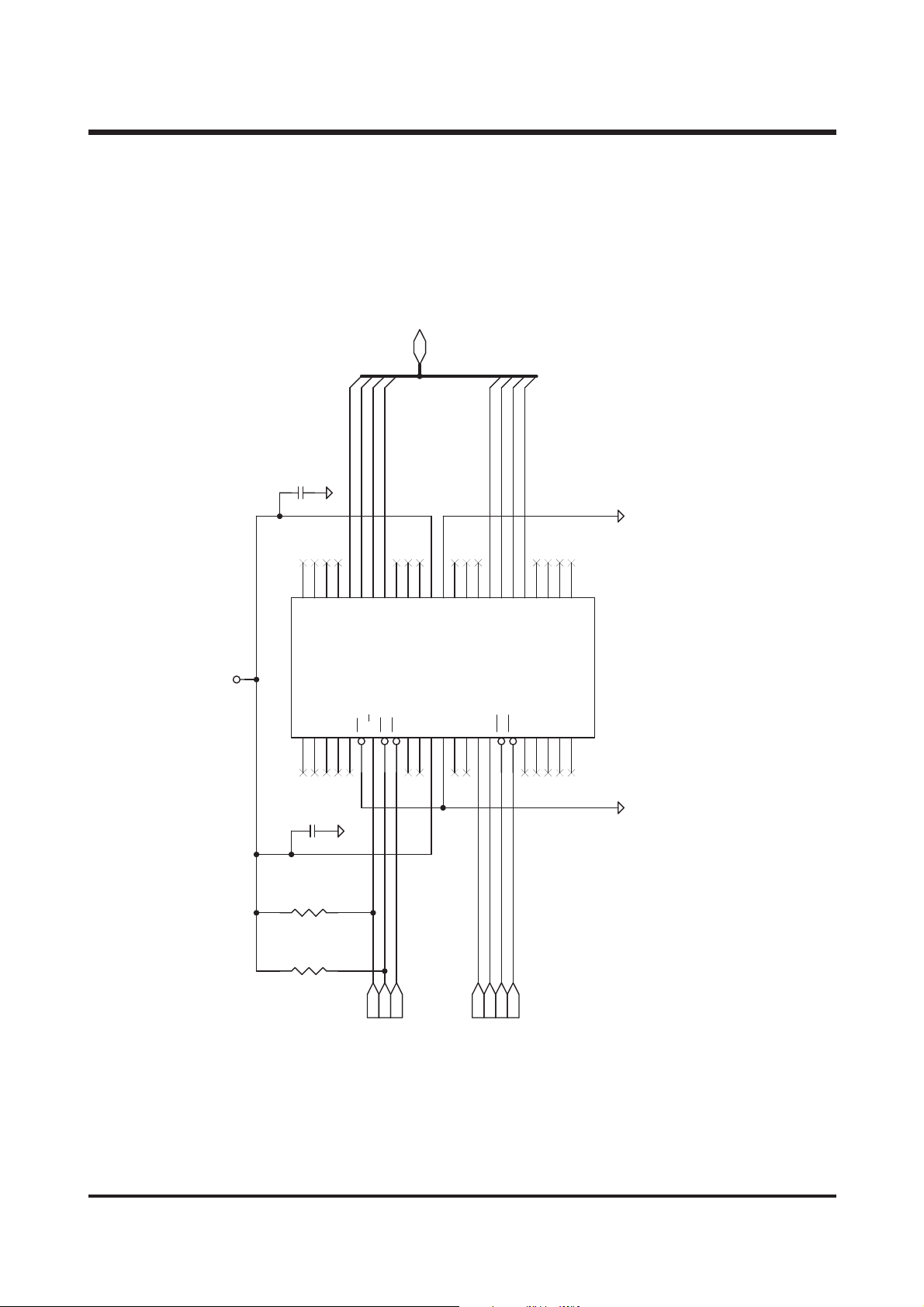
57
ⅤⅤ.. PP RR OO DD UU CCTT CC OO NN SSTTRR UU CCTTII OONN
6) 16 MBYTE NAND FLASH
NF_D[0..7]
16 MBYTE NAND FLASH
P3V3_SDR
C96
U14
104P
C0402
48
NC
NC
1
C97
104P
46
47
NC
NCNCNC
243
C0402
NF_D7
444342
45
NC
NC
56789
NF_D4
NF_D5
NF_D6
403938373635343332313029282726
41
I/O7
I/O6
I/O5
SE
R/BRECENCNC
NC
NCNCNC
I/O4
101112131415161718
Vcc
Vss
Vcc
VssNCNC
NCNCNC
NF_D2
NF_D3
I/O3
CLE
ALEWEWP
NF_D1
I/O2
I/O1
19
NF_D0
NCNCNC
I/O0
NCNCNC
202122
NC
23
2524
NCNC
K9F2808U0A
TSOP-48P
NAND FLASH (16M BYTE~128M)
R134
10K
R135
10K
R0402
R0402
NF_CE
NF_RE
NF_BUSY
NF_ALE
NF_CLE
NF_WE
NF_WP
Page 58

58
ⅤⅤ.. PP RR OO DD UU CCTT CC OO NN SSTTRR UU CCTTII OONN
7) SD CARD
FMGPIO-9
FMGPIO-10
FMGPIO-5
FMGPIO-7
4
SOT-23-5
5
3
12
U16
1
5
OUT
IN
C98
2
104P
GND
C0402
1/2 PIN
J5
34
NCON
SHORT
3
1
2
SOT-23_0.95
AAT4250
R0402-3P
R144
R143
R142
R141
R140
R139
R138
10K
10K
10K
10K
10K
10K
10K
R0402
R0402
R0402
R0402
R0402
R0402
R0402
SD_D1
SD_D2
9811
DATA2
DATA1
CD/DAT3
CMD
GND
SD1
1234567
SD_DET1
10
GND
Detect1
VDD
CLK
GND
SD_DET2
PIN 10 CARD DETECT
PIN 12 CARD PROTECT
12
Detect2
DATA
SD_ALPS_CON
SD/MMC
C253NCC0402
SD CARD
SD/MMC CONNECTOR
P3V3_SYS
SD_PWRON
C99
10uF/6V3
+
A
TANT-
R137
10K
R0402
SD_D3
SD_CMD
FMGPIO-2
FMGPIO-11
SD_CLK
SD_D0
FMGPIO-3
FMGPIO-8
Page 59

59
ⅤⅤ.. PP RR OO DD UU CCTT CC OO NN SSTTRR UU CCTTII OONN
8) MSK1151 TFT INTERFACE
P15V+/-1V
N15V+/-1V
TFT1
NCNCVSS
VC1
VC2
VGLNCVGH
VDDCPGRES
123456789
1011121314151617181920212223242526272829303132
GPCK
GSRT
0~7V5(P-P)
STBYB
VCOM
STH
STBYB
RIT
POL
STB
CLK
D05
D04
D03
D02
D01
D00
P5V+/-0V5
VSH
VSS
VSC
VRH
0V5~4V5
0V5~4V5
P3V~3V6
VRL
VDD
33
MSK1151
FPC-SJ032076-33P
MSK1151 TFT INTERFACE
C100
D3
RB501V-40
SOD323
P15V_TFTP15V_TFT
A5V_TFT
A5V_TFT
105P
12
C0805
N15V
R146
45
R0402
30K
C101
3
SOT-25
12
R145
3K 1%
22R
78
RPC1-4
TFT_CP
C103
105P
C102
2u2/16V
C104
10uF/16V
C0402
104P
R148
10K
R0402
22R
22R
22R
34
56
5 6
RPC1-2
RPC14-3
RPC17-3
T
TFT_GPCK
TFT_GRES
TFT_GSR
C0805
C0805
+
C1206
4
11V6
U18
-
+
3
1
4V4
3V7
R0402
4V4
22R
22R
12
78
RPC1-1
RPC17-4
T_STH
TF
-0.9+4V5
R154
10K
R0402
2
VR1
20K
2 5
NJM2125F
SOT-25_0.95A
C0402
C105
104P
R0402
R152
19K1 1%
22R
22R
56
7 8
3 4
RPC14-4
RPC14-2 22R
RPC1-3
Y
T
TFT_RI
TFT_STB
MVR22
22R
22R
34
1 2
RPC14-1
RPC17-2
TFT_D5
K
T_STB
TFT_CL
TF
1 3
R159
40K2 1%
R158
10K 1%
POL
TFT_
22R
22R
22R
78
7 8
5 6
RPC16-4
RPC11-4
RPC11-3
2
TFT_D4
TFT_D3
TFT_D
R0402
R0402
22R
22R
1 2
3 4
RPC11-1
RPC11-2
TFT_D0
TFT_D1
TFT_D[0..5]
1V88
0V91
4V28
A5V_TFT
3V
R168
1K
13uA
P3V3_SYS
R171
12K
R0402
R0402
R170
47K
R169
12K
R0402
+
R0402
C109
C108
C107
P5V_SYS A5V_TFT
C106
10uF/6V3
104P
C0402
C0402
104P
C0402
104P
A
TANT-
4mA
R172
220K
C110
104P
C113
104P
C111
10uF/6V3
+
C112
104P
R0402
C0402
C0402
A
TANT-
C0402
3V3=5mA
5V =7.5mA
15V=2.1mA
Page 60

60
ⅤⅤ.. PP RR OO DD UU CCTT CC OO NN SSTTRR UU CCTTII OONN
9) SD/ USB/ LED/ BUZZER
P3V3_SYS
OPI
1
MIC1
Q4
DTB113ZK
AGCOUT
C114
104P
R175
5K1
R174
150K
OPO
2
R0805
A3V3_DSP
USB_LINK
2
SOT23
10k
1
3
SOT-23-B
P3V3_SYS
C0402
R0402
R0402
C116
B14
L0603
0R
BEAD
B13
L0603
0R
BEAD
MIC
R178
1K
R0402
R173
0R
1k
3
1
2
suspend use
R176
470K
R0402
C0402
220P
C118
R180
R0402
R177
1K5
R0402
B11
B3
0R
USB_CON1
MICP
104P
C0402
NC
C117
R0402
1K
C119
100uF/6V3
+
USB_D-
R0402
R179
27R
BEAD
L0603
CP160808T301Y
BEAD
L0603
123
D-
VCC
SHIELD
6
C0402
TANT-B
USB_D+
BEAD
D+
SHIELD
758
AGC
C122
10uF/10V
R183
470K
C115
VREF
MICN
C0402
C123
104P
R184
1K
R0402
R1871KR0402
R181
27R
R0402
R182
39K
C121
C120
B12
L0603
CP160808T301Y
4
N.C
SHIELD
C0805
R0402
10uF/10V
C0805
NEAR BGA
C0402
C255
22P
C254
22P
C0402
USB_DET
R0402
C0402
10P
10P
C0402
R186
100K
R185
100K
C125
20P
C0402
C124
20P
C0402
C257
NC
C0402
GND
SHIELD
9
AGND
AGND
AGNDAGND
AGND
GPIO-1
C126
104P
R188
47K
R0402
R0402
USB-MINI
C0402
R0402
67
P3V3_SYS
345
1
2
USB CON
R0402
R189
47K
USB
89
VIDEO_DET
R0402
R190
10K
C127
22P
4
56
P3V3_SYS
R198
C0402
C126
NC
AUDIO_OUT
L0603
JACK-AJ245S-5B
J1
416
5
L15 NC
C0402
C128
104P
BEAD
R197
C0402
100R
BEAD
10K
R0402
B8 L06030R
B6 L06030R
B7 L06030R
C131
330P
C130
L0603
L9
MCI321611
270P
R202
100R
VIDEO_OUT
P3V8_VCC
R0402
R191
0R
0R
R196
R0402
NC
R195
R0402
0R
R194
R0402
R193NCR0402
VS2GND
123
SOT-23-6
U21
RST VDD
VS0 VS1
1 65234
R0402
R192
1K
RESETB
3
3
P3V3_SYS
Q5
DTC143XKA
SOT2
4.7K
2
R0402
LED-KM252003
LED1
RED
SELF_TIMER_LED
BEAD
TV OUT
C0402
C0402
R0402
103P
C129
C0402
R0402
0R
R201
R0402
NC
R200
R0402
NC
R199
SOT-26
DS9801
PRESET 2V9
POWER ON RESET
1
10K
1
3
2
SOT-23-B
SELF TIMER LED
GPIO-19
J2
P3V3_SYS
C186
105P/25V
3
1
2
CON1x3-DIP
TXD
RXD
L10
22mH
L0805
3
AUDIO
ALL NC
10K
R0402
R276
R277
C0805
R274
C184
P3V3_SYS
R203
510R
R0402
BUZ1
1
2
SOT-23-B
10K
R0402
25
R0402
10K
105P/25V
C0805
AUDIO
3
4.7K
LED2
GREEN
KP-3015
RS-232
2
1
BUZZER
SOT23
Q7
DTC143XKA
1
3
4.7K
2
GPIO-17
BUZZER
AUDIO_OUT
R0402
R275
75R
C0805
C185
105P/25V
4
SOT-25_0.95A
NJM2125F
U28
-
+
3
1
C187
R273
R278
10K
R0402
A3V3_DSP
3
1
Q6
DTC143XKA
SOT2
10K
2
3
SOT-23-B
GPIO-18
RDY_BUSY_LED
SD/USB/LED/BUZZER
R0805
10K
BUZZER
45
3
SOT-25
12
C188
104P
C0402
A3V3_DSP
4u7/10V
C0805
10K
R0402
1
2
READY/BUSY LED
Page 61

61
ⅤⅤ.. PP RR OO DD UU CCTT CC OO NN SSTTRR UU CCTTII OONN
10) POWER MODULE
1 2
20mA
J3
2
1
LED_BL
CON1X2-DIP
12
22uH
T
BAT
C133
P3V3_SYS
TP30
OUT2-2
P3V8_VCC
102P
C0402
R204
15K 1%
3 4
Q9
32
SND0403
C134
103P
C0402
0
TP6
TP31
OUT2-1
OUT1-2
R0402
15
22k
C135
10uF/10V
T-23
AO3400
SO
1
10uF/10V
C1206
R210
R209
R208
0
TP6
OUT1-1
C136
R206
R205
R211
C1206
10K
95K3 1%
10K
R207
10uF/10V
10K
301K 1%
3
4
6.8+0.7V
12
SOT-23-5
5
Q8NCSOT-25_0.65
R279
0R
R0402
7.5~8.5V
D4
RB501V-40
SOD323
L11
POWER CH1
STEP-UP
OUT2_REF
OUT1_REF
PWR_ON:High Active
PWR_CCD:High Active
PWR_BL_ON:High
Active
OUT4
OUT3
OUT3_REF
C132
36R5 1%
R0603
22k 22k
22k
3
R0402
R0402
R0402
R0402
100K
C1206
R213
R212
R0402
R0402
2
SOT-23-A
OUT1-1
LOB_STATUS
GPIO-6
0R
R0402
68K1 1%
R0402
4
4
4
12
LED_BL_ON
R216
15K 1%
R215NCR0402
LDO_FB
LDO_OUT
OUT4_REF
C137
R217
R214
15K 1%
0.7V
Q10
UMC2N
P5V_CCD
R221
0R
OUT2_REF
OUT1_REF
POWER CH2
REF4_ON
R0402
LOB_IN
C138
C0402
104P
36
LBO
AI
37
AO
38
OUT1-1
39
OUT1-2
40
OUT2-1
41
OUT2-2
42
NC
43
PVCC
44
NC
45
PGND
46
OUT3
47
OUT4
48
DTC4
123456789
R219
1K
REF4_ON
102P
C0402
C139
104P
R0402
10K
R218
15K 1%
R0402
R0402
P5V_SYS
5
15
SOT-25_0.6
22k
3 4
C142
R0603
+
12
D5
RB501V-40
SOD323
32
L12
10uH
SND0403
T
STEP-UP
BAT
C0402
104P
C140
R223
R0402
R220
1K
LBI
FB1
CS1
INE1
DTC1
U23
AT1382A
LQFP-48P
FB4
INE4
CS4
CTL4
DTC3
R0402
R222
1K
C0402
C141
104P
C146
+
47uF/6V3
TANT-B
C143
Q11
C145
C144
104P
R0402
1K
CTL1
DTC2
FB3
INE3
R0402
C0402
4u7/6V3
22k 22k
22k
10uF/10V
AO3400
1
10uF/10V
C0402
FB2
CS3
101112
TANT-A
C1206
T-23
SO
C1206
CS2
INE2
CTL3
CSCP
T
5V_TFT
12mA
P3V3_CCD
P12V_CCD
P1
R230
R0603
R228
1
1
2
4
3
12
SOT-23-5
5
RESETB
1
A
3
12
SOT-23-
OUT2-1
C151
224P
C0402
C150
C0402
224P
2526272829303132333435
CTL2
CT2
24
ENLD
23
CTL
22
VB
21
CT
20
RT
19
POR
18
VCC
17
VCC
16
VBG
15
AGND
14
AGND
13
VREF
C149
C0402
224P
C0402
C148
224P
C1206
C147
4u7/16V
R2310RR0603
UDZS3.9B
R0603
12
0R
12
OUT3_REF
D6
RB501V-40
SOD323
1 3
5
6
T1
T-N8_P3V3_P15
TRANSFORMER-8P
3
4
T
BAT
FLYBACK
POWER CH3
R227
30K
R0402
R226
30K
R0402
C0402
C153
104P
C0402
100P
C152
R0402
R229
20K 1%
C154
P3V8_VCC
R225
33K
R0402
R233
R232
R0402
R224
33K
65mA
C158
10uF/16V
C1206
C156
10uF/10V
D7
SBS004
SOT-23
7
2
TANT-B
C155
100uF/6V3
R235
NC
R0402
R0402
R234
75K
10uF/10V
C1206
R0402
75K
R0402
100K
1
R236
R0603
0R
C1206
12
8
3
3mA
N8V_CCD
D8
RB501V-40
32
A
12
SOT-23-
C157
C159
SOD323
T-23
Q12
AO3400
SO
1
OUT3
1
3
LED_BL_ON
PWR_ON
GPIO-7 GPIO-16
CCD_ON
10uF/16V
PreView Mode:3V/400mA (1.2W)
StartUp:>=1V6
ShutDown:<=1V2
C1206
10uF/10V
C1206
3
R239
120mA
2
P3V3_SYS
2.42~2.44
3V3
4
3
12
Q15 AO3401
SOT-23-A
3
12
SOT-23-A
Q14
RT9161-33CV
3V8
R0603
R238
0R
A
3
12
SOT-23-
T-23
Q13
AO3401
SO
R0603
R237
0R
P3V8_VCC
OUT4_REF
3
12
SOT-23-A
POWER CH4
STEP-UP
Strobe Charge:2V8/500ma/<10s
PreView+Charge:2V8/1A (2W8)
LOB Ref = 1V22
100K 1%
R0402
55mA
P2V5_SYS
T-23
SO
32
2
OUT
VIN
3
32
D9
1 3
L13
10uH
BATT
PWR_ON
PWR_ON
LOB_IN
T
BAT
1
GND
+
1
R240
SBS004
SOT-23
32
SND0403
CCD_ON
LED_BL_ON
CCD_ON
LED_BL_ON
LOB_TEST
C164
102P
C0402
R241
113K 1%
H=3V~2V4
TEST
L=2V3~2V2
C166
NC
C0402
R242
37K4 1%
SOT-23
1
C165
100uF/6V3
TANT-B
+
C160
47uF/6V3
TANT-B
C162
10uF/10V
C1206
R0402
1M
C1206
C161
10uF/10V
1
C1206
C163
10uF/10V
STATUS
LOB_
LOB_TES
LOB_STATUS
R0402
TEST
C167
+
R0402
47uF/6V3
1
RESETB
RESETB
R245
43K2 1%
3
4.7K
E=2.0
TEST
LOB_TEST
GPIO-5
TANT-B
R0402
R244
40K2 1%
LDO_OUT
1
3
2
SOT-23-B
4.7K
REF4_ON
1
T-23
AO3400
SO
Q16
C168
NC
R0402
R243
0R
OUT4
POWER MODULE
REF4_ON
R0402
1
10K
2
3
Q17
DTC143XKA
SOT2
1
3
2
SOT-23-B
1
(LDO USED AO3401)
LDO_FB
1
3
1
3
Q18
DTC143XKA
SOT2
1
10K
2
C0402
PWR_ON
Page 62

62
ⅤⅤ.. PP RR OO DD UU CCTT CC OO NN SSTTRR UU CCTTII OONN
11) POWER SOUR CTRL
PWR_ON
R247
100K
R0402
C171
104P
C0402
3
45
12
2
2
1
3
D11
DAN202U
SOT-323_UMT
SOT-23-5
3
5
Q19
UMC2N
SOT-25_0.6
P3V8_VCC
22k 22k
15
22k
22k
3 4
C170
104P
C0402
21
3
SOT-323
R250
POWER ON SW
P3V3_SYS
XTAL_MODE
100K
R0402
R251
2MA1
5
MA
3
4
MA
MA
MA
MA0
POWER SOUR CTRL
C252
NC
C0402
R256
10K
R0402
R255
10K
R253
10K
R0402
R0402
R254
10K
R0402
R252
10K
R0402
10K
R0402
BATT
D10
1N4001
D1FS4
P3V3_SYS
12
C169
104P
1
BAT
R246
C0402
12
22K
R0402
B9
QP1608Y121T1
C172
104P
C0402
GPIO-2
PWR_DET
BATTERY 3V
LR6-AA x 2
2
BAT
R248
22K
R0402
C173
104P
C0402
BEAD
BEAD
L0603
B10
L0603
QP1608Y121T1
C174
321
PWR_SW
GPIO-15
ADPTER_DET
104P
C0402
GPIO-14
PWR_KEEP
R0402
R249
47K
C0402
C175
104P
SYSTEM SETTING
POWER SOURCE
1 : ONE CRYSTAL MODE
XTAL_MODE
0 : USE INTERNAL CPU
0 : USE BUILD-IN USB TRANSCEIVER
0 : NORMAL RESET(10ms)
00 : 6MHz CRYSTAL
0 : GPIO[7:0] AND PORT1[7:0] SERVE THEIR DEFAULT FUNCTION
MA2
MA5
MA[4:3]
MA1
MA0
J4
DC-JACK
SHD-1303
Page 63

63
ⅤⅤ.. PP RR OO DD UU CCTT CC OO NN SSTTRR UU CCTTII OONN
12) CONNECTOR
2
+
JP1
+++++
13579
TT BATT P5V_SYS
BA
PWR_SW
SW_COL0TRIGGER
PWR_SW
6810
4
+++
+
CHARGE
READY
SW_COL2
12
+
+
FLASH CON
11
SW_COL1
AGND
CON-B064-12P
1
CONNECTOR
FLASH_CONN SMD
P3V3_SYS
10K
10K
10K
READY
CHARGE
10K
10K
TRIGGER
1 2
3 4
R258
JP2
R257
5 6
7 8
SW_COL2
SW_COL2
RP3-1
RP3-2
2
+
+++
135
RP3-3
RP3-4 10K
SW_COL3
SW_COL5
SW_COL1
SW_COL1
SW_COL5
684
+++
+
++
7
910
SW_COL0
SW_COL4
KEY CON
CON-1000LM/10P
KEY CON SMD B TO B
SW_COL3
SW_COL1
SW_COL2
SW_COL0
SW_COL[0..5]
SW_COL4
SW_COL5
SW_COL3
SW_COL0
SW_COL4
Page 64

64
ⅤⅤ.. PP RR OO DD UU CCTT CC OO NN SSTTRR UU CCTTII OONN
13) GPIO FMGPIO DIGTV MAP
CASIO TFT
TFT_D0
TFT_D1
TFT_D2
TFT_D3
TFT_D4
TFT_D5
TFT_STBYB
TFT_RIT
TFT_GSRT
TFT_GRES
Color STN
CSTN_D0
CSTN_D1
CSTN_D2
CSTN_D3
CSTN_FRAME
CSTN_FR
CSTN_SHIFT CLK
CSTN_LATCH
CSTN_ON
CSTN_BL_EN
I/O MAP
DIGTV-0
DIGTV-1
DIGTV-2
DIGTV-3
DIGTV-4
DIGTV-5
DIGTV-6
DIGTV-7
DIGTV-8
DIGTV-9
CF
CF_CE1
CF_REG0
CF_CD2
CF_CD1
CF_WATT
CF_RDY
CF_RST
CF_WE
MMC
MMC_CS
MMC_SCK
MMC_RDY
MMC_SI
MMC_WP
TFT_POL
TFT_STB
TFT_STH
DIGTV-10
DIGTV-11
DIGTV-12
CF_OE
CF_A0
CF_A1
MMC_RST
MMC_SO
TFT_GPCK
TFT_CP
TFT_DCLK
DIGTV-13
DIGTV-14
DIGTV-15
CF_A2
CF_D0
CF_D1
DIGTV-16
DIGTV-17
DIGTV-18
CF_D2
CF_D3
CF_D4
DIGTV-19
DIGTV-20
DIGTV-21
CF_D5
CF_D6
CF_D7
CF_A3
CF_A4
CF_A5
CF_A6
CF_A7
CF_A8
CF_A9
CF_A10
GPIO FMGPIO DIGTV MAP
SD
SD_D3
SD_CLK
SD_DET1
SD_DET2
SD_D0
SD_D1
SD_D2
SD_CMD
SMC
SMC_CE
SMC_ALE
SMC_CD1
SMC_BUSY
SMC_CLE
SMC_WP
SMC_RE
SMC_WE
SMC_D0
SMC_D1
SMC_D2
SMC_D3
SMC_D4
SMC_D5
SMC_D6
SMC_D7
NAND FALSH
NF_CE
NF_BUSY
NF_ALE
I/O MAP
FMGPIO-0
FMGPIO-1
FMGPIO-2
FMGPIO-3
FMGPIO-4
Description
1=Video Plug In Detect
1=USB Plug In Detect
0=Power Button Press
1=Flash Charge Control
0=Flasg Charge Ready
I/OIIIOIOIOOOOOOIOOOOOOOOOIIIIIII
FMGPIO-5
FMGPIO-6
FMGPIO-7
0=2V4 1=2V2 Battery Test
0=Batt low then 2V4 or 2V2
1=3V3CCD,12VCCD,N8VCCD ON
NF_CLE
NF_WP
NF_RE
FMGPIO-8
FMGPIO-9
FMGPIO-10
NF_WE
NF_D0
NF_D1
NF_D2
FMGPIO-11
FMGPIO-12
FMGPIO-13
FMGPIO-14
1=Flash Strobe Control
1=Keep System Power ON
NF_D3
NF_D4
NF_D5
NF_D6
FMGPIO-15
FMGPIO-16
FMGPIO-17
FMGPIO-18
1=TFT Back Light ON
1=LED ON
NF_D7
FMGPIO-19
FMGPIO-20
FMGPIO-21
FMGPIO-22
1=LED ON
0=USB Host Link Request
1=EEPROM Enable
FMGPIO-23
FMGPIO-24
FMGPIO-25
0=Lens Focus In Macro Posistion
FMGPIO-26
FMGPIO-27
FMGPIO-28
FMGPIO-29
I/OIO
D301
RXD
TXD
I/O MAP
P3.0 RXD
P3.1 TXD
P3.2 INT0
1=DC Adpter Plug In
MS_IN1=MSHUTTER DSP.N3
IOOOI
0
0
P3.3 INT1
P3.4 T0
P3.5 T1
P3.6 WR
P3.7 RD
P1[0..7] NoUsed
I
D301
VIDEO_DET
USB_DET
POWER_DET
SP533 EVB
VIDEO_DET
USB_DET
SW_POWER
I/O MAP
GPIO-0
GPIO-1
GPIO-2
FLASH CHARGE
FLASH RDY
LOB_TEST
LOB_STATUS
CCD_ON
FLASH CHARGE
FLASH RDY
VBAT_SET
VBAT_VALUE
15V_EN
GPIO-3
GPIO-4
GPIO-5
GPIO-6
GPIO-7
ROM_A16
ROM_A17
ROM_A18
ROM_A16
ROM_A17
ROM_A18
GPIO-8
GPIO-9
GPIO-10
ROM_A19
FLASH TRIG
XTAL_MODE
ROM_A19
FLASH TRIG
XTAL_MODE
GPIO-11
GPIO-12
GPIO-13
POWER_KEEP
ADPTER-DET
TFT_BL_ON
BUZZER_OP
POWER_EN
5V_EN
18V_EN
BUZZER_OP
GPIO-14
GPIO-15
GPIO-16
GPIO-17
RDY/STBY LED
SELF TIMER LED
USB_LINK
EE_EN
EE_SCK
RDY/STBY LED
SELF TIMER LED
QUENCH_LVL
AF IN1
AF EN
GPIO-18
GPIO-19
GPIO-20
GPIO-21
GPIO-22
EE_SIO
APER_CUR
SW_COL0
AF IN2
ZOOM EN
SW_ROW1
GPIO-23
GPIO-24
GPIO-25
SW_COL1
SW_COL2
SW_COL3
SW_ROW2
SW_ROW3
SW_ROW4
GPIO-26
GPIO-27
GPIO-28
SW_COL4
SW_COL5
VD_IV5
SW_MODE1
SW_MODE2
GPIO-29
GPIO-30
GPIO-31
VD_IV6
VD_CH5
MS_IN1
MSHUTTER-DIR
GPIO-32
GPIO-33
GPIO-34
AP_IN1
AP_IN2
APTURE_DIR
APTURE_EN
SW_MODE3
GPIO-35
GPIO-36
GPIO-37
GPIO-38
SW_MODE4
PHOTO_RST
GPIO-39
GPIO-40
GPIO-41
Page 65

65
Ⅵ. TROUBLESHOOTING
11..
PPRRIINNCCIIPPAALL TTRROOUUBBLLEESSHHOOOOTTIINNGG
1) Each kind of assembly problem
When you repair defective camera, check the condition of soldering and connection of PCB at first.
Following pictures are examples.
Damaged LCD connector Short-circuited buzzer L/W
Dirt in the power S/W Incomplete connection of lens connector
Short-circuited MIC L/W Wrong connected MIC L/W
Page 66

66
ⅥⅥ.. TTRROO UU BB LL EESS HHOO OO TT IINNGG
Short-circuited CCD PIN(1) Short-circuited CCD PIN(2)
Short-circuited CCD PIN(3) Short-circuited CCD PCB
Bad soldering on CCD PCB Wrong connected CCD PCB
Page 67

67
ⅥⅥ.. TTRROO UU BB LL EESS HHOO OO TT IINNGG
Bad connection of CCD F-PCB(1) Bad connection of CCD F-PCB(2)
Damaged CCD connector Short-circuited SUB condenser
Incomplete soldering on card holder Short-circuited card holder pin
Page 68

68
ⅥⅥ.. TTRROO UU BB LL EESS HHOO OO TT IINNGG
Damaged shutter MG L/W Overfull soldering on shutter MG L/W
Short-circuited shutter F-PCB Shutter IRIS is out of position
Wrong connected soldering on IRIS L/W Bad soldering IRIS L/W
Page 69

69
ⅥⅥ.. TTRROO UU BB LL EESS HHOO OO TT IINNGG
Disconnected TFT LCD L/W Bad connection of TFT LCD connector
Transformed MICRO S/W(1) Transformed MICRO S/W(2)
Short-circuited battery L/W Battery lead wire
Page 70

70
2) POWER ON problem
ⅥⅥ.. TTRROO UU BB LL EESS HHOO OO TT IINNGG
Check the power source
(Battery, Adaptor etc.)
1. Check the condition of DC JACK(short-circuited,
transformed) (See p. 73)
2. Check the power LEAD WIRES.
3. Check the connection between MAIN PCB(JP1) and
FLASH PCB(JP1). (See p. 71)
1. Check the soldering condition of each parts.
2. Check the each parts condition. (See p. 72, 73)
1. Check the soldering condition of the part.
2. Check the part condition. : 27MHz (See p. 73)
1. Check the soldering condition of each parts.
2. Check the each parts condition. (See p. 72, 73)
1. Check the soldering condition of each parts.
2. Check the each parts condition. (See p. 72)
MAIN PCB error
Check the connection
of each PCB
MAIN(JP1) + FLASH(JP1)
Check the parts listed below
(Q10, Q13, Q14, Q15, Q16, Q18)
Check the part listed below
(Y2)
Check the parts listed below
(R10, R11, R207,
B9, B10, D6, D10)
Check the parts listed below
(L11, L12, L13)
Page 71

71
KEY PCB
Check the connection,
dirt and damage.
ⅥⅥ.. TTRROO UU BB LL EESS HHOO OO TT IINNGG
Check the connection,
dirt and damage.
Check the connection,
dirt and damage.
XE TUBE
R83
C97
48
1
D2
1
D1
TP8
JP1
1
b
U14
1
C96
R64
R142
R134
R141
R135
J3
C134
Q9
C135
D4
R208
R211
Q10
C146
C136
R232
C138
R219
C139
R212
R217
U23
C148
R222
C141
C153C152
C154
Q6
C157
R203
LED2
B13
B14
RPC2
RPC22
RPC20
C16
L10
Y2
L14
Y1
C25
C14
C33
R8
R11
GC1
R179
B2
C20
C19
R181
R10
C93
J5
C99
C145
Q11
C161
D9
C163
R243
Q16
C168
C164
Q17
R238
Q14
R223
C49
R230
C50
C159
R228
D6
C156
R236
C158
D8
R231
U4
D7
C120
C155
Q12
Q4
R177
B11
B12
C125
R186
R185
C121
C187
R176
USB_CON1
T
R
9
JP2
10
C24
C4
C11
C15
C1
C8
C28
D1
C41
RPC1
U16
C165
C88
C86
R145
R152
C105
R148
1
U6
C52
R20
C59
C60
C45
J1
G
1
J2
RPC7
R112
2
R73
RPC10
C22
U13
C31
C5
C18
C92
C6
C30
C21
C29
C122
C2
C9
C115
C3
C114
C13
R54
R52
R50
L1
C10
C23
C27
C12
C17
C170
C98
C171
C106
R168
C101
R18
R16
C61
C79
R12
RPC24
C7
R79
R253
R28
RPC25
R192
R252
R57
R193
RPC16
R255
R246
C172
Q19
R80
U21
D11
C110
C129
R195
R247
C103
C102
D3
2
C100
1
C104
R146
R154
VR1
U18
R158
R159
C55
C54
L3
R21
R17
R19
C53
C69
C68
C67
C46
C42
C75
C48
C47
1
C72
C174
C80
J4
MAIN PCB(BOT)
R201
C113
R172
C109
TFT1
33
C78
C76
U7
D2
C74
C73
C81
C82
C71
C70
L6
L7
8
U8
R22
B9
R249
C175
R248
d
TFT LCD
C5
D3
D1
Q2
Q1
BATT
BATT
PWR_SW
G
CHARGE
SW_COL1
TRIGGER
SW_COL3
SW_COL2
D5U
READY
AGND
AGND
D4
FLASH V3.0
-
L2009402
M3361
R2
C9
S1
L1
R1
2003/10/1
R10
C1
R12
SW1
B1
R9R7B2
R8U1C8
C6
R11
R6
B3
R5
C10
VCC
U2
MA REV: 3.0
-
M3361
PAN
1
FLASH PCB
48
1
a
C117
C255
MIC1
L2009304
2003-10-03
R218
C137
R213
JP1
11
12
C119
B8
C128
C254
R187
R184
R178
R180
B3
C124
B5
R188
R182
C126
T1
LED1
Q5
R214
R198
R229
R205
C144
R216
R225
R210
R206
C132 R204
R233
R234 R226
C150 C151
C133
R209
C149
R220
R215
C140
R227
R207
R224
R241
R235
R239
C147
R221
C142
2
D5
L11
Q8
R143
R279
C143
R258
11
SD1
R130
C94
C91
B1
C95
Q7
BUZ1
C38
U12
R144
R88
C90
R82
R92
12
R189
C184
R275
R197
C169
C186
R245
L13
L12
C32
C26
R1
R5
R4
R3
C35
B7
R190
C185
R277
R276
R274
BAT2
R202
B10
C130
C173
U28
C188
R278
L9
B6
R273
C127
1
C131
R14R13
1
RP1
L4
8
C62
RP2
L2
C57
1
C83
C84
R244
C166
R242
Q15
C167
C160
C162
Q13
R240
C89
Q18
R237
27
R137
R138
R250
8
R173
10
R2
R6
R7
R9
C40
C39
C34
C36
R110
RPC21
RPC23
R100
R95
RP3
BAT1
D10
L8
C44
C43
L5
48
37
C65
C51
FPC1
C58
U5
C66
25
R15
2
1
24
C64
C56
C63
54
Q1
R25
Q2
C85
C87
U10
R111
R58
R256
RPC14RPC17
U2
RPC4
RPC3
R257
C111
C112
R171
C107
R169
R170
C108
28
R191
R200
R196R194
R105
R139
C253
R251
C252
R199
R254
RPC15
RPC11
RPC18
RPC13
C37
RPC6 RPC5
C123
R175
C118
C116
R183
R174
R97
RPC9 RPC8
RPC12
R140
RPC19
R70
13
R63
c
MAIN PCB(TOP)
26 FPC1 1
FIG. CONNECTION
a MAIN(JP1) - FLASH(JP1)
b MAIN(JP2) - KEY(JP1)
JP2
C7
R1
C6
C3
C1
D1
D2
IR6
IR3
C5
C8
C2
R2
R5
C4
Q1
R4
JP1
c MAIN(FPC1) - CCD(FPC1)
d MAIN(TFT1) - TFT LCD
CCD F PCB
Page 72

72
ⅥⅥ.. TTRROO UU BB LL EESS HHOO OO TT IINNGG
◆◆ MMAAIINN PPCCBB ((TTOOPP))
LL11 22
LL11 33
LL11 11
R207 (Malfunction may takes place
in voltage mode)
T1 (Transfomer)
◆Check the Terminal No.5 15V(LCD)
Check the Terminal No.6 3.3V(CCD)
Check the Terminal No.8 -8V(CCD)
Q13 (For SYS power supply, 3.8V)
◆Check the Terminal No.2 3.8V(OUT)
Q18 (Power S/W Control)
Check JP1 whether it is opened or s
hort-circuited
◆Can't turn the camera power off
Check L11, L12, L13 whether those are opened or not
◆Connect each terminal with battery and check the
voltage
Q15 (SYS power supply)
◆Check the Terminal No.2 3.3V
Check the Terminal No.3 2.5V
Check B10 whether it is opened or not
◆◆
Check VCC voltage of each terminal
Check D10 whether it is opened or not
◆Check VCC voltage of each terminal
Page 73

73
ⅥⅥ.. TTRROO UU BB LL EESS HHOO OO TT IINNGG
◆◆ MMAA IINN PPCCBB ((BBOOTT))
Check Y2(27MHz) whether it is
opened or s
hort-circuited
Q14 (SYS power supply)
◆Check the Terminal No.2 2.5V(OUT)
Check the Terminal No.3 3.8V(IN)
Check B9 whether it is opened or not
◆Check VCC voltage of each terminal
Check D6 whether it is opened or not
◆Check VCC voltage(15V, TFT LCD)
Check R10 and R11 whether it is opened or not
◆When the camera turns off automatically
Check Q16 whether it is opened or not
Check Q10 whether it is opened
or s
hort-circuited
◆Check No.4 pin(5.0V)
Check J4 whether it is s
hort-circuited
or not
◆Do not use any battery, use AC adapter
Page 74

74
3) Aperture operation error
ⅥⅥ.. TTRROO UU BB LL EESS HHOO OO TT IINNGG
Check the connection between
LENS MODULE and MAIN PCB
AE METER in the LENS MODULE
error
Check the U7 part condition
1. Check the connection between CCD F PCB and
MAIN PCB(FPC-1).
2. Check the soldering condition of CCD F PCB and
SHUTTER F PCB. (See p. 71)
Check the soldering condition whether
it is opened or s
hort-circuited
1. Check whether the ohm value of the AE METER is
20Ω or not.
Check the soldering condition whether it is opened or s
hort-circuited
Check the ohm value(
20Ω) of each terminal
Page 75

75
ⅥⅥ.. TTRROO UU BB LL EESS HHOO OO TT IINNGG
Check the FPC-1, whether it is
opened or s
hort-circuited
Check the U7(S/H, IRIS control driver), whether
it is opened or not
◆Check NO.4(+) and 6(-) out put terminal
Page 76

76
4) Image error(No image, Noise on image...)
ⅥⅥ.. TTRROO UU BB LL EESS HHOO OO TT IINNGG
Check L5, whether it is opened or s
hort-circuited
◆Check the voltage, whether it is 3.0V or not
Check D1, whether it is
opened or s
hort-circuited
Check C2, whether it is
opened or s
hort-circuited
Check the R2, whether it is
opened or s
hort-circuited
Check Q1, whether it is
opened or s
hort-circuited
◆When the captured image don't play back on the LCD monitor.
Check the CCD, whether it is opened or s
hort-circuited
Check the connection between
LENS MODULE and MAIN PCB
Check the parts listed below
(Q1, C2, D1, R2, L5)
Check the soldering condition
of CCD
1. Check the connection between CCD F PCB and
MAIN PCB(FPC-1). (See p. 71)
1. Check the soldering condition of each parts.
2. Check the each parts condition.
Page 77

77
Check the Focus lever, whether it is
opened or s
hort-circuited
5) ZOOM operation error
ⅥⅥ.. TTRROO UU BB LL EESS HHOO OO TT IINNGG
Check the BACK COVER and
KEY PCB assembling condition
Check the focus lever
(When the focus lever
can't be operated)
Check the connection
of each PCB
1. Check the KEY PCB assembling condition.
(Dust, Assembling error, Space)
1. Check the focus lever assembling condition located
the front cover.
2. Check the lever assembling condition.
1. Check the connection between KEY PCB(JP1) and
MAIN PCB(JP2).
2. Check the connection between CCD F PCB and
MAIN PCB(FPC-1). (See p. 71)
Check the FPC-1, whether it is
opened or s
hort-circuited
Page 78

78
Check JP-1, whether it is opened
or s
hort-circuited
6) BUTTON operation error
ⅥⅥ.. TTRROO UU BB LL EESS HHOO OO TT IINNGG
Check D1, whether it is opened or s
hort-circuited
Check the BACK COVER and
KEY PCB assembling condition
Check the parts for D1
Check the connection
of each PCB
1. Check the PCB assembling condition.
(Dust, Assembling error, Space)
1. Check the connection between KEY PCB(JP1) and
MAIN PCB(JP2).
2. Check the connection between CCD F PCB and
MAIN PCB(FPC-1). (See p. 71)
Page 79

79
ⅥⅥ.. TTRROO UU BB LL EESS HHOO OO TT IINNGG
7) STROBO operation error
Check T2, whether it is opened or s
hort-circuited
Check Q2, whether it is opened or s
hort-circuited
Check the IGBT, whether it is
opened or s
hort-circuited
Check the charging voltage(C4)
Check C7, whether it is opened or s
hort-circuited
1. Check the power LEAD WIRES, whether it is
connected correctly or not.
2. Check the connection between MAIN PCB(JO1)
and FLASH PCB(JP1). (See p. 71)
1. Check the soldering condition of each parts.
1. Check the soldering condition of each parts.
FLASH PCB error
Check the connection between
MAIN PCB(JO1) and
FLASH PCB(JP1)
Check the parts listed below
(T1, MAIN CON. U1)
When the strobo error takes place,
check the parts listed below
(IGBT, Q2, C4, T2,C7)
Page 80

80
8) Problem aboout TFT LCD
1. Check the connection between MAIN PCB(TFT1) and
TFT LCD F PCB. (See p. 71)
1. Check the soldering condition of the part.
TFT LCD error
TFT LCD F PCB
Check the connection
MAIN(TFT1) + TFT LCD
Check the soldering of
TFT LCD L/W on MAIN PCB
Check the U18 on MAIN PCB
Check if the U18 (TFT LCD Generator IC) is open
ⅥⅥ.. TTRROO UU BB LL EESS HHOO OO TT IINNGG
Page 81

81
22.. DDIISSAASSSSEEMMBBLLEE TTHHEE CCAAMMEERRAA
1. Remove the 8 screws of the camera.
2. Open the battery cover and remove the 3 screws on the internal camera.
3. Disassemble the front cover.
※ Before disassembling the front cover,
disassemble the MIC connecter first.
ⅥⅥ.. TTRROO UU BB LL EESS HHOO OO TT IINNGG
Page 82

82
4. To disassemble the back cover, remove the 3 screws as shown below.
5. Remove the back cover and top cover.
6. To disassemble the barrel, remove the 3 screws and disassemble the FPCB from the connector.
ⅥⅥ.. TTRROO UU BB LL EESS HHOO OO TT IINNGG
Page 83

83
7. Disassemble the barrel.
8. To disassemble the TFT LCD, remove the solder of lead wire. Release the TFT LCD lock and
disasssemble the FPCB.
9. Disassemble the TFT LCD.
ⅥⅥ.. TTRROO UU BB LL EESS HHOO OO TT IINNGG
Page 84
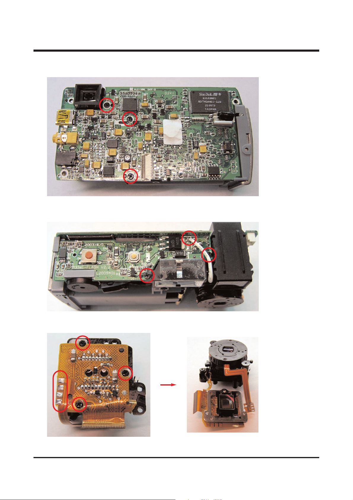
84
10. To disassemble the MAIN BOARD, remove the 3 screws.
11. Remove the 2 screws on the FLASH BOARD and remove lead wire.
12. To disassemble the BARREL ASS'Y, remove the solder on the CCD F PCB and the 3 screws.
ⅥⅥ.. TTRROO UU BB LL EESS HHOO OO TT IINNGG
Page 85

85
13. To disassemble the BACK COVER ASS'Y, remove the screw.
14. When you assemble the back cover, assemble the mode dial spring shown as below.
15. Screw down the back cover.
ⅥⅥ.. TTRROO UU BB LL EESS HHOO OO TT IINNGG
 Loading...