


SERVICE MANUAL
MODEL : CI3352X/TSECX CHASSIS : P68SC & RM109
COLOUR TELEVISION RECEIVER

Features :
SAFETY CAUTION :
Before servicing this model, it is important that a service technician refers to the "Safety Precaution" and "Product Safety Notice" described in the technical Service Manual.
Voltage synthesized tuning System, On-screen Display, Auto-fine Tuning, Dark
Tube, Auto Brightness/Contrast Control, 29-Key Transmitter.
* For continued X-radiation, replace the picture tube with original type
* Design and specifications are subject to change without prior notice.
* WARNING-SHOCK HAZARDS - Use an isolation transformer when servicing
For Safe Use
- 1. Read all of these instructions.
- 2. Save these instructions for later use.
- 3. Unplug this television receiver from the wall outlet before cleaning. Do not use liquid cleaners or aerosol cleaning.

- Do not use attachments not recommended by the television receiver manufacturer as they may cause hazards.
- 5. Do not use this television receiver near water for example, near a bathtub, washbowl, kitchen sink, or laundry tub, in a wet basement, or near a swimming pool, etc.
- 6. Do not place this television receiver on an unstable cart, stand, or table. The television receiver may fall, causing serious injury to a child or an adult, and serious damage to the appliance. Use only with a cart or stand recommended by the manufacturer, or sold with the television receiver. Wall or shelf mounting should follow the manufacturer's instructions, and should use a mounting kit approved by the manufacturer.
- 7. Solts and openings in the cabinet and the back or bottom are provided for ventilation, and to insure reliable operation of the television receiver and to protect it from overheating, these openings must not be blocked or covered. The openings should never be blocked by placing the television receiver should not be placed in a built-in installation such as a bookcase unless proper ventilation is provided.
- 8. This television receiver should be operated only from the type of power source indicated on the marking label. If you are not sure of the type of power supplied to your home, consult your television dealer or local power company. For television receivers designed to operated from battery power refer to the operating instructions.

9. This television receiver is equipped with a polarized alternating-current line plug(a plug having one blade wider than the other.) This plug will fit the power outlet only one way. This is safety feature. If you are unable to insert the
plug fully into the outlet, try reversing the plug. If the plug should still fail to fit, contact your electrician to replace your obsolete outlet. Do not defeat the safety purpose on the polarized plug.
If your television receiver has a threewire grounding-type plug, please note the following. This television receiver is equipped with a 3-wire grounding type plug(a plug having a third(grounding) pin). This plug will only fit into a grounding type power outlet. This is a safety feature. If you are unable to insert the plug into the outlet, contact your electrician to replace your obsolet outlet. Do not defeat the safety purpose of the grounding plug.

10.Do not allow anything to rest on the power cord. Do not locate this television receiver where the cord will be abused by persons walkling on it.

- 11.Follow all warmings and instructions marked on the television receiver.
- 12.If an outside antenna is connected to the television receiver, be sure the antenna system is grounded so as to provide some protection against voltage surges and built up static charges. Section 810 of the National Electrical Code, NFPA No. 70-1975, provides information with respect to proper grounding of the mast and supporting structure, grounding of the lead-in wire to an antenna discharge unit, size of gounding conductors, location of antenna dicharge unit, connection to grounding electrodes, and requirements for the grounding electrode. See Figure 1.

- 13.For added protection for this television receiver during a lightening storm, or when it is left unattended and unused to long periods of time, unplug it from the wall outlet and disconnect the antenna. This will prevent damage to the receiver due to lighten and power-line surges.
- 14.An outside antenna system should not be located in the vicinity of overhead power lines or other electric light or power circuits, or where it can fall into such power lines or circuits. When installing an outside antenna system extreme care should be taken to keep from touching, such power lines or circuits as contact with them might be fatal.
- 15.Do not overload wall outlets and extension cords as this can result in fire or electric shock.
- 16.Never push objects of any kind into this television receiver through cabinet slots as they may touch dangerous voltage points or short out parts that could result in a fire or electronic shock. Never spill liquid of any kind on the television receiver.
- 17.Do not attempt to service this television receiver yourself as opening or removing covers may expose you to dangerous voltage or other hazards. Refer all servicing to a qualified service personnel.
18.Unplug this television receiver from the wall outlet and refer servicing to a qualified service personnel under the following conditions.
a.When the power cord or plug is damaged or frayed.
- b.If liquid has been spilled into the television receiver.c.If the television receiver has been exposed to rain or water
- d.If the television receiver does not operate nomally by following the operating instructions. Adjust only those controls that are covered by the operating instruction as improper adjustment of ther controls may result in damage and will often require extensive work by a qualified technician to restore the television receiver to a nomal operation.
- e.If the television receiver has been dropped or the cabinet has been damaged.
- f.When the television receivers exhibits a distinct change in performance-this indicates a need for service.
- 19. When replacement parts are required, be sure the series technician has used replacement parts specified by the manufacturer that have the same characteristics as the original part. Unauthorizd substitutions may result in fire, electric shock, or other hazards.
- 20.Upon completion of any service or repairs to this television receiver, ask the service technician to perform routine safety checks to detemine that the television is in safe operating condition.
- 21. Television equipment and car combination should be moved with care. Quick stops, excessive force, and uneven surfaces may cause the equipment and cart combination to overturn.

For Service Manuals Contact MAURITRON TECHNICAL SERVICES 8 Cherry Tree Rd, Chinnor Oxon OX9 4QY Tel:- 01844-351694 Fax:- 01844-352554 Email:- enquiries@mauritron co.uk
PRODUCT SAFETY NOTICE
Many electrical and mechanical parts in this chassis have special safety-related characteristics. These characteristics are often passed unnoticed by visual inspection and the protection afforded by them cannot necessarily be obtained by using replacement components rated for higher voltage, wattage, etc. The replacement parts which have these special safety characteristics are identified in this manual and its
supplements:
electrical components having such features are identified by shading on the schematic diagram and the parts list. Before replacing any of these components, read the parts list in this manual carefully. The use of substitute parts which do not have the same safety characteristics in the parts list may create a shock, fire, X-radiation or other hazards.
SERVICE NOTES
1.when replacing the parts or the circuit boards, clamp the lead wires to the terminals before soldering.
2. When replacing a high wattage resistor (oxide metal film resistor) in the circuit board, keep the resistor 10mm (1/2 in) away from the circuit board.
3.Keep the wires away from high voltage or high temperature components.
4.If any fuse in this TV receiver is blown, replace it with the FUSE specifiled in the chassis parts list.

| * IN CASE OF | PULL THE CHASSIS-RAIL | * IN CASE OF | |
| 3312 SERIES | TO BESIDE (1) THEN | 3351 SERIES | |
| 3313 SERIES | SEPARATE THE CHASSIS | 3352 SERIES | |
| 3315 SERIES | (②) | 3357 SERIES | |
| 3325 SERIES | 3852 SERIES | ||
| 3327 SERIES | 3857 SERIES | ||
| 5012 SERIES | CHASSIS | 5051 SERIES | |
| 5013 SERIES | 5052 SERIES | ||
| 5015 SERIES | 5057 SERIES | ||
| 5025 SERIES | |||
| 5026 SERIES | Contraction , | ||
| 5027 SERIES | CHASSIS | ||
| 5322 SERIES | -RAIL | ||
| 3351 SERIES |
AT FIRST PUSH THE LOCK SWITCH,((UTHEN
TAKE OUT THE CHASSIS. (2)) CODE NO ; 36114-699-710 |
X-RADIATION PRECAUTION
1 The excessive high voltage can produce potentially hazardous X-RADIATION. To avoid such hazards the high voltage must not exceed the specified limit. The nominal value of the high voltage of this receiver is 24 0KV at zero beam current (minimum brightness). The high voltage must not, under any circumstances, exceed 30KV. Each time a receiver requires servicing and the high voltage should be checked following the HIGH VOLTAGE CHECK procedure in this manual. It is recommended that the reading of the high voltage should be recorded as a part of the service record
It is important to use an accurate and reliable high voltage motor
- 2 The only source of X-RADIATION is thos TV receiver it is the nicture tube For continued X-RADIATION protection the replacement tube must be exactly the same type as specified in the parts list
- 3 some parts in this receiver have special safety related characteristics for X-RADIATION protection. For continued safety, the parts replacement should be undertaken only after referring to the PRODUCT SAFETY NOTICE.
SAFETY PRECAUTION
Warning : The serivce should not be attempted by anyone unfamilliar with the necessary precautions in this receiver. The followings are the necessary precautions to be observed before servicing
Since the chassis of this receiver is directly connected to the AC power line-(Hot chassis), an isolation transformer should be used during any dynamic service to avoid possible shock hazards.
- 1. Always discharge the picture tube anode to the CRT conductive coating before handling the picture tube. The picture tube is highly evacuated and if broken, the glass fragments will be violently expelled. Use shatterproof goggles and keep the picture tube away from the bare body during a handling
- 2. When replacing a chassis in the cabinet, it is always certain that all the protective devices are put back in place, such as non - metallic control knobs, insulating covers, shields, isolation resistor-capacitor network, etc.
- 3 Before returning the set to the customer, always perform an AC leakage current check on the exposed metallic parts of the cabinet, such as antennas, terminal, screwheads, metal overays, control shafts, etc. To be sure the set is safe to operate without danger of electrical shock. Plug the AC line cord directly to the AC outlet (do not use a line isolation transfomer during this check). Use an AC voltmeter having 5000 ohm per volt or more sensitivity in the following manner. Connect a 1500 ohm 10 watt resistor, paralleled by a 0.15 µ F,AC type capacitor, between a good earth ground(water pipe.conduit etc.)and the exposed metallic parts, one at a time. Measure the AC voltage across the combination of 1500 ohmresistor and 0.15µ F capacitor. Reverse the AC plug at the AC outlet and repeat the AC voltage measurements for each exposed metallic part. The measured voltage must not exceed 0.3volts RMS. This corresponds to 0.2 milliamp AC. Any value exceeding this limit constitutes a potential shock hazard and must be corrected immediately.

Figure 1.AC Leakage Current Check
MAURITRON TECHNICAL SERVICES 8 Cherry Tree Rd, Chinnor Tel:- 01844-351694 Fax:- 01844-352554 Email:- enquiries@mauritron.co.uk
For Service Manuals Conta
TABLE OF CONTENTS
| 1.INSTRUCTIONS |
|---|
| 2.CHASSIS BLOCK DIAGRAM |
| 3. POWER SUPPLY SECTION |
| 1.BLOCK-DIAGRAM |
| 2.INTRODUCTION 3-4 |
| 3.IC SPECIFICATION (SDH209B) |
| 1)Block-Diagram |
| 2)Electrical Characteristics |
| 4.CHROMA, VIDEO, IF, SOUND, DEFLECTION SECTION |
| 1.IC SPECIFICATION(TDA8362) |
| 2)Block-Diagram |
| 3)Pin Function |
| 2.CHROMA VIDEO SECTION |
| 1)Block-Diagram |
| 2)Actuating Description |
| 3)IC Block-Diagram (TDA 8362) 7 |
| 4)IC Specification (TDA 8395) 7-8 |
| 5)IC Specification (TDA4661) 8-9 |
| 3.IF SECTION |
| 1)Block-Diagram 9 |
| 2)Actuating Description 9-10 |
| 3)IC Block-Diagram (TDA 8362) 10 |
| 4.SOUND SECTION |
| 1)Block-Diagram 10 |
| 2)Actuating Description 10 -11 |
| 3)IC Block-Diagram (TDA8362) 11 |
| 4)IC Specification (TDA1013A) 11 |
| 5.DEFLECTION SECTION |
| 1)Block-Diagram |
| 2)Actuating Description | . 12 |
|---|---|
| 3)IC Block-Diagram (TDA8362) | 13 |
| 4)IC Specification (KA2131) | 13 |
| 5.REMOCON SECTION | |
| 14 | |
| 2.BLOCK-DIAGRAM | 15 |
| 3.PIN FUNCTION | 15 - 16 |
| 6.ALIGNMENT and ADJUSTMENT | |
| 1.GENERAL INFORMATIONS | 16 |
| 2.AUTOMATIC DEGAUSSING | 16 |
| 3.HIGH VOLTAGE CHECK | 16 |
| 4.HORIZONTAL PHASE ADJUSTMENT | 16 |
| 5. VERTICAL HEIGHT ADJUSTMENT | 17 |
| 6.SCREEN ADJUSTMENT | 17 |
| 7.FOCUS ADJUSTMENT | 17 |
| 8.R-F AGC ADJUSTMENT | 17 |
| 9. COLOUR PURITY ADJUSTMENT | 17 |
| 10.CRT WHITE BALANCE ADJUSTMENTS | 17 |
| 11.CONVERGENCE ADJUSTMENTS | |
| 1)Centre Convergence Adjustment | 17 - 19 |
| 2)Circumference Convergence Adjustment | 19 |
| 12.VIF(SIF) ADJUSTMENT | 19 |
| 7.TELETEXT SECTION (OPTION) | |
| 1.TTX BLOCK DIAGRAM | |
| 2.SEMICONDUCTOR SPECIFICATION | 20 - 26 |
| 8.TROUBLESHOOTING CHARTS | 27 - 30 |
| ANSERTING FROM OF THE IMPORTANT PARTS | 31 |
| 10.CHASSIS REPLACEMENT PARTS LIST | 32 - 37 |
| 11.EXPLODEO-VIEW & PARTS LIST | 38 - 39 |
| 12.SCHEMATIC-DIAGRAM | 41 - 42 |
| 13.PWB PATTERN & LOCATION | 43 |
мемо
| МЕМО | |
|---|---|
1.INSTRUCTIONS
1.IC LINE UP
| Loc No | Specification | Description | Remarks |
|---|---|---|---|
| IC101 | TDA8362 |
PAL/NTSC/SECAM Decoder
(VIF/SIF/VIDEO,Chroma/Deflection) |
|
| IC502 | TDA8395 | SECAM Decoder | |
| IC501 | TDA4661 | 1 H Delay | |
| IC301 | KA2131 | Vertical output | |
| RIC01 | SPM-109 | 8bit µ — com | |
| RIC02 | X24C02P | ||
| IC102 | LA7910 | BAND Docoder | |
| IC602 | TDA1013A | Sound output Amplifier | |
| IC801 | SDH209B | PWM-Controller for SMPS | |
| XIC01 | SAA3010 | Remote Control | |
2.MEANS OF COMPONENTS NUMBER SERIES
| 100 Series TUNER/IF/AFT/AGC | 500 Series Chroma/peaking processing |
|---|---|
| processing | 600 Series Sound processing |
| 200 Series Video/Luminance processing | 700 Series Video/Chroma switchingSection |
| 300 Series Vertical deflection | 800 Series AC input, power supply circuits |
| 400 Series Horizontal deflection | 900 Series CRT Driver Section |
3.ABBREVIATION
| ABCL | : Automatic Brightness Contrast Limiting | LLD | : Low Level Detector |
| ABL | : Automatic Beam Limiting | LPF | : Low Pass Filter |
| AC | : Alternating Current | MTS | : Multi Television Sound |
| ACC | : Automatic Color Control | NFB | : Negative Feed Back |
| AFC | : Automatic Frequency Control | NTSC | : National Television System Comittee System |
| AFT | : Automatic Fine tuning | NVRAM | : Non-Valatile Random Access Memory |
| AGC | : Automatic Gain Control | PAL | : Phase Alternating by Line System |
| AM | : Amplitude Modulation | PCM | : Pulse Coded Modulation |
| APC | : Automatic Phase Control | PIF | : Picture Intermediate Frequency |
| APL | : Average Picture Level | PLL | : Pulse Locked Loop |
| AVC | : Automatic Volume Control | PWM | : Pulse Width Modulation |
| DB | RAM | : Random Access Memory | |
| DC | : Direct Current | RF | : Radio Frequency |
| DIP | : Dual-in-line Package | SAW | : Surface Acoustic Wave |
| DY | : Deflection York | SIF | : Sound Intermediated Frequency |
| D/A | : Digital to Analog | S/N | : Signal Noise |
| FB | : Fast Blanking | I 2 C | : Inter Intergrated Circuit |
| FRT | : Flyback Trans | DAC | : Digital Analog Convertor |
| FM | : Frequency Modulation | BPF | : Band Pass Filter |
| HDT | : Horizontal Drive Trans | OSD | : On-Screen Display |
| C | : Integrated Circuit | SCL | : Serial Clock Line |
| E | SDA | : Serial Data Line |
For Service Manuals Contact MAURITRON TECHNICAL SERVICES 8 Cherry Tree Rd, Chinnor Oxon OX9 4QY Tel:- 01844-351694 Fax:- 01844-352554 Email:- enquiries@mauritron.co.uk
2.CHASSIS BLOCK DIAGRAM

3.POWER SUPPLY SECTION
1.BLOCK-DIAGRAM

For Service Manuals Contact MAURITRON TECHNICAL SERVICES 8 Cherry Tree Rd, Chinnor Oxon OX9 4QY fel:-01844-351694 Fax:-01844-35255 Email:- enquiries@mauritron.co.uk
2.INTRODUCTION
The IC SDH209 controls the bipolar switching transistors and performs all necessary regulation and function in free running flyback converters.
The flyback converter is the most cost saving SMPS for CTV and VCR. But as the frequency goes up according to the increase of the input AC voltage and the reduction of power consumption an abnormal oscillation like intermittent oscillation or over voltage can happen easy unless the frequency rise is restrained.
SDH209 having a built-in mono-multi vibrator which is triggered at transistor switched off and generates a pulse of constant width to keep the transistor off for the pulse period, will keep switching frequency less than 120KHz.
SDH209 having a built-in constant DC current source will achieve the small drive power consumption at higher AC input and achieve the sufficient drive current at lower AC input.
Owing to the above two built-in circuits, SDH209 can get good regulation and high efficiency over a wide AC input range and keep stable oscillation at very small load.
In the standard connections, the constant voltage charged up at the capacitor is used and also used to sense voltage. So, the transformer and circuit are both simple.
Free running frequency of flyback converter is expressed by the following formula.
where, LP Primary inductance
- Pin : Input power
- ns : Secondary winding turns
- np : Primary winding turns
- Vin : Input DC voltage
Vo : Output DC voltage
As the above formula, the frequency f goes up according to the increase of Vin and the decrease of Pin.
Mono-multi vibrator built-in SDH209 restrains the rise of switching frequency.
This mono-multi vibrator generates 4µsec pulse every end of Ton period.
That is, this mono-multi vibrator is triggered by signal which is produced when the transistor is switched off. The transistor is unable to be switched on again while the mono-multi vibrator's output is high.
While the transistor is off, the primary inductance of transformer and the floating capacitance or capacitor installed across the snubber diode compose a resonant loop and oscillate. This resonant frequency depends on the primary industance and capacitance.
When 4µsec over, the transistor is released to be switched on again. The time of switch on is approximately 4µsec plus half cycle of resonant frequency from the time of switch off.
Capacitors installed across the snubber diode, across the secondary diodes and across C-E of the transistor affect to the resonant frequency. In order to obtain the stable stand-by oscillation, a total equivalent capacitance is recommended to be less than 330pF. Total equivalent capacitance Ceq is calculated.
Ceq = Csn + Sce +
- 3 -
where, Csn : Across the snubber diode
- Cce : Across C-E of the transistor
- np : Primary winding turns
- ns1 : Secondary winding S1 turns
- ns2 : Secondary winding S2 turns
- Cs1 : Across the diode of S1
- Cs2 : Across the diode of S2
Remarks : Capacitance includes a diode junction capacitance and a floating capacitance. Oscillation at no load is stable and its power loss is small because of the above mechanism.
Operation of Over Load
The formula of frequency f shows that f goes down when Vo is smaller than the rated value. When the switch is turned on, Vo starts from zero.
Therefore, the ordinary SMPS makes the whistle sound when starting up.
But, Ton limiter built-in SDH209B limits Ton duration regardless of Vo value.
So, no whistle is made at starting up.
This Ton limiter also works as a protector when the transistor is switching at the over load. Particularly when the input AC voltage is lower than the rated value, Ton becomes longer and the saturation loss increases. But Ton limiter stops becoming longer and protect the transistor from thermal run away.
Operation at Output Short
When the input AC voltage is higher than 220V. Ton limiter is not enough to protect the transistor from the over current. So, the current limiter is provided.
The instantaneous locus at the output short has not been taken clear in the picture. But the locus is expanded to 680V and 3.8A. Therefore, transistor's SOA is required bigger than this point. When the output short is further continued, the locus becomes shrinked and even a dead short will not destroy the transistor.
Because the constant DC current source for base drive is empty due to the dead short and then the transistor does not switch at a large current.
Transformer
1)Primary and Secondary Turn Ratio The value of (Np/Ns) - Vo is factor to determine switching duty, Ic peak, Vce peak and frequency. The recommended value is like the below
2)Leakage Inductance
The recommended value is 1% of the primary industance.
3)Magnetic Saturation Current
4×10⁻³ + 0.6
Where, Lp : Primary inductance (H) r : Current sense resistor (Ω)
3.IC SPECIFICATION (SDH209B)
1)Block-Diagram


| Para- | Symbol | Ratings | 6 | Pomarks | |
|---|---|---|---|---|---|
| Meter | (unit) | MIN | TYP | MAX | Remarks |
|
Supply
Voltage |
V1(V) | +10.4 | |||
| Range Pin 1-2 | V2(V) | -3.0 | -18.0 | ||
|
Output
Current |
l 3 (mA) | 73 | |||
|
Reference
Voltage |
v 4 (V) | 8.5 | 8.8 | 9.1 | |
|
Reference Voltage
Ambient Temperature |
Kt(mv/℃) | -3.0 | |||
|
Mono Multi
Frequency |
T 1 (jµis) | 7.5 | |||
| Ton Limit | T 2 ((µ∣s) | 18 | 22 | 26 | |
|
Current
protection |
V 8 (V) | -0.6 | |||
|
Reference Voltage
Adjust Range |
V 4 (V) | 8.0 | 10.0 | ||
4. CHROMA, VIDEO, IF, SOUND, DEFLECTION SECTION
1.IC SPECIFICATION (TDA8362)
1)Introduction
a) General Description
Vision IF amplifier, video demodulator, video amplifier, AGC and AFC are suitable for both negative and positive modulation.
Sound limiter, demodulator and amplifier with volume control.
Inputs and switches for external audio and CVBS signals.
Synchronization circuit with drive circuits for horizontal and vertical deflection.
Separate supply pin for starting the horizontal oscillator from the main rectifier.
X-ray protection (combined with the 2nd phase detector nin)
PAL/NTSC colour decoder in which the chroma filters (bandpass and trap) and the luminance delay line have been integrated. The circuit has a separate chroma input and the filters can be switched-off so that S-VHS signals (via an external switch) can be applied to the IC.
For SECAM applications an(alignment-free) SECAMdecoder can be added to the IC.
Peaking circuit in the luminance channel.
RGB-output circuit with linear inputs for On-Screen
Character Display
The supply voltage for the IC is 8 Volts. It is mounted in an S-DIL envelope with 52 pins.
b)Features
-
Multi-standard vision IF circuit
- (positive and negative modulation)
- Multi-standard FM sound demodulator (4.5MHz to 6.5 MHz)
- Video and audio switches
- (CVBS int/ext, S-VHS and audio int/ext)
- Integrated chroma trap and bandpass filters (auto-calibrated)
- Luminance delay line integrated
- PAL/NTSC colour decoder with automatic search system
- Easy interfacing with the TDA 8395 (SECAM decoder) for multi-standard applications.
- RGB-control circuit with linear RGB inputs and fast blanking
- Horizontal synchronization with two control loops and an alignment-free horizontal oscillator Vertical count-down circuit and a vertical pre-amplifier
- Low dissipation (only 600 mW)
- Small amount of peripheral components compared with completion IC's.
- Only one adjustment (vision IF demodulator)

- 5 -
3)Pin Function
| No | Function | No | Function |
|---|---|---|---|
| 1 | Audio deemphasis | 52 | Decoupling bandgap supply |
| 2 | IF-demodulator tuned circuit | 51 | Decoupling sound demodulator |
| 3 | IF-demodulator tuned circuit | 50 | Audio output |
| 4 | Video indentification output | 49 | Tuner take-over adjustment |
| 5 | Sound IF in plus volume control | 48 | AGC decoupling capacitor |
| 6 | External audio input | 47 | Tuner AGC output |
| 7 | IF video output | 46 | IF-input |
| 8 | Decoupling digital supply | 45 | IF-AFC output |
| 9 | Ground | 44 | AFC output |
| 10 | Positive supply (8 V) | 43 | Vertical output |
| 11 | Ground | 42 | Vertical ramp generator |
| 12 | Decoupling filter tuning | 41 | Vertical feedback input |
| 13 | Internal CVBS input | 40 | Ø-1 loop filter |
| 14 | Peaking control input | 39 | Ø 1- loop filter |
| 15 | External CVBS input | 38 | Flyback input / sandcastle output |
| 16 | Chroma + A/V switch input | 37 | Horizontal output |
| 17 | Brightness control input | 36 | Start horizontal oscillator |
| 18 | B-output | 35 | 4.43мнz X-tal connection |
| 19 | G-output | 34 | 3.58мнz X-tal connection |
| 20 | R-output | 33 | Loop filter burst phase detector |
| 21 | RGB-insertion and blanking input | 32 | 4.43MHz output for TDA 8395 |
| 22 | R-input for insertion | 31 | B-Y output signal |
| 23 | G-input for insertion | 30 | R-Y output signal |
| 24 | B-input for insertion | 29 | R-Y input signal |
| 25 | Contrast control input | 28 | B-Y input signal |
| 26 | Saturation control input | 27 | Hue control input (or chroma out) |
2.CHROMA VIDEO SECTION
1)Block-Diagram
For Service Manuals Contact MAURITRON TECHNICAL SERVICE 8 Cherry Tree Rd, Chinnor Oxon OX9 4QY Tel:-01844-351694 Fax:-01844-3525

2)Actuating Description
- Colour Decoder
The colour decoder contains an alignment-free X-tal oscillator, a dual killer circuit and the colour difference signals demodulators. The decoder adapts automatically for PAL and NTSC signals. Two X-tal pins are present so no external switching is required. With the SECAM add-on decoder TDA8395 an alignment free multi-standard
decoder can be built with an automatic selection. This makes the application of the TDA8362 very flexible. The following applications are possible:
- PAL/SECAM:
In this application pin 27 is not used for Hue-control but for the chroma signal for the SECAM add-on circuit. Pin 27 has to be connected to the supply line 8V via a series resistor of 10k a . Together with the alignment-free SECAM add-on circuit TDA8395 a PAL/SECAM decoder is realized.
The burst phase detector locks the X-tal oscillator with the burst signal. Two gain modes provide an increased catching range when the PLL is unlocked and a low ripple voltage and a good noise immunity when the PLL is locked.
The burst phase detector operates during the burst key period only, to prevent the PLL from being disturbed by the chroma signal.
The killer circuit switches off the R-Y and B-Y demodulators at too low input signal condition (burst amplitude). Proper hysteresis prevent the constant on/off switching at a certain input level.

4)IC Specification (TDA8395)
a)Introduction
The TDA8395 is an alignment-free SECAM colour decoder and can be used in conjunction with the TDA8362. It includes the Cloche filter, demodulator and identification circuit. The TDA8395 application needs very few external components, the deemphasis is internally calibrated.
The cloche filter is a gyrator-capacitor type filter. Its resonance frequency is controlled during the calibration period and offset during scan for the right resonance frequency. The required reference frequency for calibration must be connected at pin 1 and is obtained from the TDA8362 (pin 32).
The two(or three)-level sandcastle pulse has to be connected at pin 15 (TDA8362 pin38) and is used for
blanking periods and provides the clock information for the identification circuit.
The chroma signal at pin 16 connected to pin 27 of TDA8362, is demoduleted by a PLL demodulator, which uses the reference frequency and a bandgap reference to force the PLL to the desired demodulation characteristic.
Digital line identification is implemented to check the incoming signal for SECAM. If SECAM is detected, pin 1 will sink a current of 150µA. Together with the TDA8362 the voltage at this pin will become high (5.5V). In this case the colour difference signal outputs will be switched on. These outputs will be disconnected and the high-ohmic when no SECAM is detected for two frame periods, the demodulator will be initialized before trying again.


c)Pin Function
| No | SYMBOL | Function |
|---|---|---|
| 1 | f ref/ IDENT | reference frequency input/identification input |
| 2 | TEST | test output |
| 3 | Vp | positive supply voltage |
| 4 | n.c. | not connected |
| 5 | n.c. | not connected |
| 6 | GND | ground |
| 7 | CLOCHEref | Cloche reference filter |
| 8 | PLLref | PLL reference |
| 9 | - (R-Y) | - (R-y) output |
| 10 | - (B-Y) | - (B-Y) output |
| 11 | n.c. | not connected |
| 12 | n.c. | not connected |
| 13 | n.c. | not connected |
| 14 | n.c. | not connected |
| 15 | SAND | sandcastle pulse input |
| 16 | CVBS | video (chrominance) input |
5)IC specification (TDA4661)
a)Introduction
The TDA4661 are integrated the baseband delay lines of 64µS for colour television receivers. It can be connected to the
b)Block-Diagram
TDA8362 and TDA8395 without the need of switches and alignments. The TDA4661 consists of two main blocks:
-Two comb filters with a delay time of 64µ sec in switched capacitor technique.
-Internal clock generation of Змнz, line locked via the sandcastle pulse.
The TDA4661 operates according to the mode demanded by the colour transmission standard. In the PAL mode it operates as a geomentric adder to satisfy the requirements of PAL demodulation, in the NTSC mode it reduces the cross-colour interference (comb-filtering) and in the SECAM mode the delay line repeats the colour difference signal on consecutive horizontal scan lines
The colour difference signals are AC-coupled to pin 14 and 16 and clamped by the input stages. The internal clock drives the delay lines to obtain the required 64 µ sec. The clock pulses are derived from a 6MHz Current Controlled Oscillator which is the line locked via a PLL with the sandcastle pulse, connected at pin 5. Sample and hold low pass filters suppress the clock signal. The delayed and the un-delayed signals are added, buffered and fed to the output pins 11 and 12.
For Service Manuals Contact MAURITRON TECHNICAL SERVICES 8 Cherry Tree Rd, Chinnor Oxon OX9 4QY Tel:- 01844-351694 Fax:- 01844-352554

- 8 -
c)Pin Function
| No | Symbol | Function | No | Function | |
| 1 | Vp 2 |
+8V Supply Voltage
for analogue part |
9 | Vp1 |
+8V Supply Voltage
for analogue part |
| 2 | n.c. | not connected | 10 | GND1 |
ground for analog
part(0V) |
| 3 | GND2 |
ground for digital
part(0V) |
11 | ‰(R-Y) |
± (R-Y) output
signal |
| 4 | i.c. | internally connected | 12 | Vo(B-Y) |
± (B-Y) output
signal |
| 5 | SAND |
Sandcastle pulse
input |
13 | n.c. | not connected |
| 6 | n.c. | not connected | 14 | Vi(B-Y) |
± (B-Y) input
signal |
| 7 | i.c. | internally connected | 15 | n.c. | not connected |
| 8 | i.c. | internally connected | 16 | Vi(R-Y) |
± (R-Y) input
signal |
3.IF SECTION
1)Block-Diagram

2)Actuating Description
a)IF amplifier
The IF-amplifier contains 3 AC-coupled control stages with a total gain control range which is in excess of 60 dB. The sensitivity of the circuit is comparable with that of modern IF-IC's. The reference carrier for the video demodulator is obtained by means of the passive regeneration of the picture carrier. The external reference tuned circuit is the only remaining adjustment of the IC. The polarity of the demodulator can be switched so that the circuit is suitable for both positive and negative modulated signals.
The AFC-circuit is driven with the same reference signal as the video demodulator. To avoid that the video content
disturbes the AFC operation a sample-and-hold circuit is applied. The capacitor for this functions is internal. The AFC output voltage range is 6 Volts.
The AGC-detector operates on top-sync or top white-level depending on the position of the demodulator. The AGC detector time-constant capacitor is connected externally. This is mainly because of the flexibility of the application. The time-constant of the AGC system during positive modulation is rather longer to avoid visible variations of the signal amplitude. To obtain an acceptable speed of the AGC system a circuit has been included which detects whether the AGC detector is activated every frame period. When 3 frame periods no action is detected, the speed of the system is increased.
The circuit contains a video identification circuit which is independent of the synchronization circuit. Therefore the search tuning is possible when the display section of the receiver is used as a monitor. The ident output voltage is low when no transmitter is identified. In that condition the sound demodulator is switched off (mute function). When a transmitter is identified the voltage is high. The voltage level is dependent on the frequency of the incoming chroma signal.
b)AGC Tuner AGC and AFC
The A.G.C. detector operates at top-sync level for signals with negative modulation and at peak-white level for positive modulated signals. This A.G.C. detector is gated for negative modulated signals to reduce the sensitivity of impulsive noise.
The time constant capacitor (C117) is connected externally at pin 48. For positive modulated signals the A.G.C. time constant is long to avoid visible variations of the video output signal. To obtain an acceptable A.G.C. speed with positive modulation an extra circuit checks whether the A. G.C. detector is activated every frame period. The speed will be increased if this circuit detects that the video output signal has not reached 80% of peak white level for approximately 100mS.
The tuner AGC take-over point can be set by adjusting the DC-voltage at pin 49, with a potentiometer of 10 kg (VR101).
The tuner A.G.C. (pin 47) is an open collector output stage with an output swing of 2mA min. The voltage swing,required by the tuner, can be obtained with an external resistor network, connected at pin 47. Pin 47 may rise 2V above the actual supply voltage, without damaging the IC.
This feature simplifies the application, because most
tuners require a 9V A.G.C. voltage level for min. gain. The A.F.C. circuit is driven by the same reference signal as the video demodulator.A sample and hold circuit avoids video break-through from the video demodulator to the A.F.C. voltage. The A.F.C. output voltage range is from 0 to Vcc, the stepness of the A.F.C. slope can be influenced by resistors R114 and R115.

3)IC Block-Diagram (TDA8362)
4.SOUND SECTION
1)Block-Diagram

2)Actuating Description
The sound bandpass and trap filters have to connected externally. The filtered intercarrier signal is fed to a limiter circuit and is demodulated by means of a PLL demodulator. This PLL circuit itself tunes automatically to the incoming signal so that no adjustment is required.
The volume is the DC-controlled. The composite audio output signal has the amplitude of 700mV RMS at maximum volume control setting. The deemphasis capacitor has to be connected externally. The noncontrolled audio signal can be obtained from this pin (via a buffer stage). The amplitude of this signal is 350mV RMS. The external audio input signal must have an amplitude of 350MV RMS. The audio/video switch is contolled via the chroma input pin.
For Service Manuals Contact MAURITRON TECHNICAL SERVICES 8 Cherry Tree Rd, Chinnor Oxon OX9 4QY Tel:- 01844-351694 Fax:- 01844-352554 Email:- enquiries@mauritron.co.uk
- 10 -
Audio input signal from an external source (SCART) with an amplitude up to 350mVrms (+/- 6 dB) can be fed to pin 6. The audio switch is controlled via the chroma input pin 16, as described in Chapter 2.1.8. The volume control operates upon the external audio input signal, when the
TDA8362 is switched to the external mode
When the TDA8362 is switched for video signals with the positive modulation, the demodulated AM-sound signal can be connected to the external audio input at pin 6 under the operation of the volume control.
3)IC Block-Diagram (TDA8362)

4) IC Specification (TDA1013A)
a)Introduction
The TDA1013A is a monolithic integrated audio amplifier cicuit with D.C. volume control in a 9-lead single in-line (SIL) plastic package. The wide supply voltage range makes this circuit very suitable for applications in mains fed apparatus such as television receivers and record players.
The D.C. volume control stage has a logarithmic control characteristic with a range of more than 80 dB; control can be obtained by means of a variable D.C. voltage between 3.5 and 8 V.
The audio amplifier has a well defined open loop gain and a fixed integrated closed loop gain. This offers an optimum in number of external components, performance and stability.
The SIL package (SOT-110B) offers a simple and lowcost heatsink connection.

b)Block-Diagram


2)Actuating Description
The incoming video signals, pin 13 for the internal signal and pin 15 for an external CVBS signal, are fed to the synchronization separator circuit. Internally the black level and the top sync. level are detected, next the synchronization pulses are amplified to a fixed level and sliced at 50% of that level. In this way a very good synchronization performance is obtained. The separated synchronization pulses are fed to the first phase detector circuit and to the coincidence detector. The components which determine the loop gain of the first phase detector are connected at pin 40 (C401, C402 and R402). The coincidence detector is only used to detect whether the line oscillator is synchronised, not for transmitter identification.
The line oscillator is running at twice the line frequency and is derived from the X-tal oscillator frequency of the colour decoder, consequently no adjustment is required. The free-running frequency has a maximum deviation of 2% compared to the nominal frequency.
The second phase detector generates the pulses for the horizontal driver stage (pin 37).
The loop filter capacitor (C404) is connected at pin 39. Horizontal shift can be obtained by a potentiometer and series resistor (R401 and R402) connected at pin 39
The TDA8362 has a separate start-up circuit for the horizontal oscillator (pin 36). In case this feature is used for starting the horizontal deflection the resistor connected at the base of the horizontal driver
transistor (Q401) must be connected to the start supply as well (pin 37 is an open collector). For applications which do not require a start-up function pin 36 must be connected to the main supply voltage (8V).
The vertical drive pulses (pin 43) are generated by a divider circuit. The vertical ramp generator components are connected at pin 42. Capacitor C311 is charged via two resistors, one resistor connected to a stabilized supply voltage (R313). In this way the vertical amplitude will be kept constant with different picture contents.
AC and DC feedback voltage from the vertical deflection stage must be connected at pin 41
3)IC Block-Diagram (TDA8362)

4)IC Specification (KA2131)
a)Introduction
b)Block-Diagram
The KA2131 is a monolithic integrated circuit designed for the vertical output stage in color television receivers.
- FUNCTIONS
- Driver stage
- Output stage.
- Flyback generator.
- Pulse shaper.
- FEATURES
Low power consumption, direct deflection coil driving capability (Flyback voltage is supplied two times as high as supply voltage during flyback period only).
High breakdown voltage : 60V

5.REMOCON SECTION
1.INTRODUCTION
CTV340S(SPM 109B) is a low cost television receiver control system bases on the PCA84C641 microcontroller. It is a voltage synthesis tuning (VST) system which can be used all over the world. All relevant control functions of the system are displayed via the on-screen display circuitry of the microcontroller. Herewith two independent lines of 16 characters with 4 different sizes and in 7 different colours can be displayed. All analogue picture settings are controlled with 4 on-chip digital to analogue convertors. The fifth digital to analogue converter can be used for volume in a mono-only option, or full sound (Voume, Bass, Treble, Balance) can be controlled in a German Stereo and/or Nicam sound configuration. This system is colour standard independent.
A four page teletxt system, based on the VIP2(SAA5231), ECCT(SAA5243) and display memory, can be controlled indirectly via a second microcontroller. This offers the possibility of a sophisticated teletext system with special features like FASTEXT, TOP, LIST, packet X/26 decoding (for Spain and Eastern Europe).A minimum amount of
software is spent to transfer the teletxt commands from the remote control to this special teletext controller. A second option is a system with no teletext at all.
The CTV340S(SPM109B) system fulfils a numerous and varied requirements and has options to make it applicable to all markets.
|
|||||
|---|---|---|---|---|---|
| ACC | Analogue to Digital Convertor | ||||
| Peri | Peripheral TV signal source | ||||
| CCT | Computer Controlled Teletext decoder | ||||
| DAC | Digital to Analogue Convertor | ||||
| l 2 C | Inter IC bus, 2-wire bidirectional multimaster bus | ||||
| IDENT | horizontal coincidence signal, transmitter IDENTification | ||||
| NV-memory | Non-Volatile memory | ||||
| OSD | On Screen Display | ||||
| PP | Personal Rreference, prefered analogue values | ||||
| RC-5 | Remote Control system, according RC-5 world standard | ||||
| VST | Voltage Synthesis Tuning | ||||
| VTR | Video Tape Recorder time constant | ||||
| MEMO | MEMO |
|---|---|
| For Service Manuals Contact | |
| Email:- enquiries@mauritron.co.uk | |

3. PIN FUNCTION
| No | Symbol | Function | No | Symbol | Function |
|---|---|---|---|---|---|
| 1 | VTUNN | tuning voltage control output | 11 | Peril | Peri output 1 |
| 2 | VOL | volume control output in mono-only option | 12 | CVBS in | CVBS status input |
| 3 | BRI | brightness control output | 13 | KEYB0 | keyboard scan line input/output |
| 4 | COL | colour control output | 14 | KEYB1 | keyboard scan line input/output |
| 5 | CON | contrast control output | 15 | KEYB2 | keyboard scan line input/output |
| 6 | HUE/ | hue control output | 16 | KEYB3 | keyboard scan line input/output |
| 7 | BND-0 | band-switch output 0 | 17 | KEYB4 | keyboard scan line input/output |
| 8 | BND-1 | band-switch output 1 | 18 | KEYB5 | keyboard scan line input/output |
| 9 | AFC | analogue AFC sense input | 19 | KEYB6 | keyboard scan line input/output |
| 10 | Peri0 | Peri output 0 | 20 | MDSTR | system mode strobe output |
| No | Symbol | Function | No | Symbol | Function |
|---|---|---|---|---|---|
| 21 | ground supply input | 32 | oscillator output | ||
| 22 | RED | OSD red output | 33 | power-on reset input/output | |
| 23 | GREEN | OSD green output | 34 | SND1 | horizontal coincidence input |
| 24 | BLUE | OSD blue output | 35 | RMOT | remote control input |
| 25 | FBL | OSD fast blanking output | 36 | VTR | VTR time constant control output |
| 26 | HSYNC | horizontal synchronization input | 37 | Sys1 | system output 1 |
| 27 | VSYNC | vertical synchronizatin input | 38 | Sys0 | system output 0 |
| 28 | DOSCOUT | LC oscillator output for OSD | 39 | SCL | I 2 C - bus clock signal input/output |
| 29 | IDENT | LC oscillator input for OSD | 40 | SDA | I 2 C - bus data signal input/output |
| 30 | test input; connected to ground | 41 | STDBY | Standby/On control input/output | |
| 31 | oscillator input; 10 MHz crystal | 42 | +5V supply voltage input |
Notes:
1) These pins are read at "cold start", they define the configuration/options of the TV-system
2) These pins can command a solenoid to switch-off AC-mains supply.
6.ALIGNMENT and ADJUSTMENT
- This Models has only one adjustment -
1.GENERAL INFORMATIONS
All the adjustments are thoroughly checked and corrected when the receiver leaves the factory. Therefore the receiver should operate normally and produce proper colour and B/W picture upon installation. However the minor service adjustments may be required depending on the particular location in which the receiver is operated. This receiver is shipped completely in carboard carton. Carefully draw out the carton and remove all the packing materials. Pulg the power cord into a convenient two pin power outlet. Turn the receiver ON and adjust the fine tuning for the best picture detail. Check and adjust all the customer controls such as BRIGHTNESS, CONTRAST and COLOUR Controls to obtain natural colour or B/W picture.
2.AUTOMATIC DEGAUSSING
A degaussing coil is mounted around the picture tube so that the external degaussing after moving the receiver is nomally unnecessary, providing the receiver is properly degaussed upon installation. The degaussing coil operates for about 1 second after the power to the receiver is switched ON. If the set is moved or faced in a different direction, the power switch must switch off at least 10 minutes in order that the automatic degaussing circuit is operated property.
If the chassis or parts of the cabinet becomes magnetized and cause poor colour purity, use an external degaussing coil.
Slowly move the degaussing coil around the face-plate of the picture tube, the sides and the rear of the receiver and slowly withdraw the coil to the distance of about 2m before disconnecting it from the AC source. If the colour shading still persists, perform the COLOUR PURITY ADJUSTMENT and CONVERGENCE ADJUSTMENTS procedures, as mentioned later.
3.HIGH VOLTAGE CHECK
CAUTION : There is no HIGH VOLTAGE ADJUSTMENT on this chassis. But B+ power must be adjusted in +125V under the full colour bar pattern and nomal picture control level.
- 1)Connect an accurate high voltage meter to the second, anode of the picture tube.
- 2)Turn on the receiver. Set the BRIGHTNESS and CONTRAST control to minimun(Zero beam).
- 3)The high voltage should be measured less.
- 4)Rotate the BRIGHNESS and CONTRAST control to the both extremes to be sure. The high voltage does not exceed the limit under any conditions.
4.HORIZONTAL PHASE ADJUSTMENT
If you want to move the center of picture, adjust HORIZONTAL phase control(VR401)
5.VERTICAL HEIGHT ADJUSTMENT
The SIZE control(VR301) on the main board changes the size of the picture, having an equal effect on the top and the bottom.
6.SCREEN ADJUSTMENT
1)Tune in an active channel.
2)Make the picture normal condition (no blooming or noflyback line) with the VR screen.
7.FOCUS ADJUSTMENT
Adjust the FOCUS control on FBT for well defined scanning lines in the center area of the screen.
8.R-F AGC ADJUSTMENT
Tune the set in the strongest station in your area. Turn the AGC control(VR101) on the IF board to fully clockwise position
3)Adjust the AGC control until noises (snow) dissappear from the screen.
9.COLOUR PURITY ADJUSTMENT
- NOTE : Before attempting any purity adjustments, the receiver should be operated for at least fifteen minutes. Purity adjustment requires Rubber Wedge kit.
- 1)Demagnetize the picture tube and cabinet using a degaussing coil.
- 2)Turn the CONTRAST and BRIGHTNESS controls to the maximum.
- 3)Receiver the green colour pattern.
- 4)Loosen the clamp screw holding the yoke, and slide the yoke backward or forward to provide the vertical green belt (zone) in the picture screen.
- 5)Remove the Rubber Wedges.
- 6)Rotate and spread the tabs of the purity magnet(See Fig.3) around the neck of the picture tube until a green belt is obtained in the center of the screen. And at the same time, center the raster vertically by adjusting the magnet.
- 7)Move the yoke slowly forward or backward until a uniform red screen is obtained. Tighten the clamp screw.
8)Check the purity of the red and blue raster.
9)Tighten the clamp screw of the yoke temporarily.
10)Obtain a white raster ; referring to the "CRT WHITE BALANCE ADJUSTMENT ".
11)Proceed with convergence adjustment.
10.CRT WHITE BALANCE ADJUSTMENT
1) preparation
a)Operate the receiver for at least 20 minutes before attempting the white balance adjustment.
- b)Receive a black and a white signals (Lion head oattern is better)
- c)Set the colour control to the center position.
- d)Set the brightness and contrast controls to the maximum position.
- e)Set the red, blue and green low light controls to the mechanical center position.
- f)Set the blue and red drive controls to the mechanical center position.
- g)Set the screen VR control on FBT to the minimum position (fully counter clockwise).
- h)Connect 1 to 2 and 3 to 4 in CN202.
2)STEPS
a)Rotate the SCREEN control on FBT (T444) gradually clockwise until the first horizontal line appears slightly on the screen.
b)Adjust the two CUT - OFF controls to obtain the sli-
ghtly lighted horizontal line in the same levels of three colours(red, green,blue).
The line look like white if the CUT - OFF controls are adjusted property.
- c)Reset the CN202 on the MAIN board to obtain a raster ("NORMAL" Position).
- d)Adjust the blue and red drive controls to obtain proper white - balanced picture in high light areas.
e)Set the contrast control to the minimum position and turn the brightness control slightly counterclockwise to obtain a dark gray raster.
- Then check the white balance in low brightness.
- If the white balance is not enough, repeat steps 1) -4) for the correct white balance.
-
11.CONVERGENCE ADJUSTMENTS
- NOTE : Before attempting any convergence adjustment, the receiver should be operated for the least fifteen minutes.
- 1)Center Convergence Adjustment
a)Receive the crosshatch pattern with a colour bar signal generator.
- b)Adjust the BRIGHTNESS and CONTRAST Controls for a well defined pattern.
- c)Adjust the two tabs of the 4-pole Magnets to change the angle among them (See Fig.2) and superimpose the red and the blue vertical lines in the center area of the picture screen. (See Fig.2).
d)Turn the both taps while at the same time keeping angle constant and superimpose the red and the blue horizontal lines at the center of the screen. (See Fig. 3).
e)Adjust the two tabs of 6-pole Mangnets to superimpose the red/blue line and green one. Adjust the angle to affect the vertical lines and
rotate both magnets to affect the horizontal lines.
- f)Due to the interaction between these adjustments the steps 3,4 and 5 should be repeated until the satisfactory results are obtained.
-
2)Circumference Convergence Adjustment
- a)Loosen the clamping screw of deflection yoke to allow the voke to tilt.
- b)Put a wedge as shown in Fig. 1 temporarily. (Do not remove the cover paper on adhesive part of the wedge).
- c)Tilt front of the deflection yoke up or down to obtain better convergence in circumference. (See Fig.3) Push the mounted wedge into the space between the picture tube and the yoke to fix the yoke temporarily.
- d)Put the other wedge into bottom space and remove the cover paper to stick.
- e)Tilt the front of the yoke right of lift to obtain the convergence in circumference. (See Fig.3)
MEMO
f)Keep the yoke position and put another wedge in either upper space. Remove the cover paper and stick the wedge on picture tube to fix the yoke.
g)Detach the temporarily mounted wedge and put in another upper space. Stick it an picture tube to fix the voke
h)After fixing three wedges recheck overall convergence. Tighten the screw firmly to fix the yoke and check the voke is firm.
i)Stick 3 adhesive tabs on wedges as shown in Fig. 1.
12.VIF (SIF) ADJUSTMENT
-
1)Equipment
- -Pattern generator (PM5518)
- Digital Voltmeter
2)Preparation
a)Set the supply voltage to AC 220V
b)Set the RF output frequency of Gen to 38.9MHz and then Multi-burst pattern.
c)Connect the RF out of PM5518 to Tuner's Pin (IF)
e)Adjust the DC voltage of J106 tape 4V by controlling the T101.
|
MEMO |
|
Eor. Service.Manuals.Contact
MAURITRON TECHNICAL SERVICES |
|
8 Cherry Tree Rd, Chinnor
Oxon OX9 4QY |
|
Email: enquiries@mauriton.co.uk |
|
|
|
|
|
|
|
|
|
|
|
|
|
|
|
|

7.TELETEXT SECTION
1. TTX BLOCK DIAGRAM(OPTION)

2. SEMICONDUCTOR SPECIFICATION
a. DESCRIPTION
The MAB8401 family of microcontrollers is fabricated in NMOS. The family consists of 5 devices:
- MAB8401 128 bytes RAM, external program memory, with 8-bit LED-driver(10mA), emulation of MAB/F8422/42 * possible
- MAB/MAF8411 1K byts ROM/64 bytes RAM plus 8-bit LED-driver
- MAB/MAF8421- 2K byts ROM/64 bytes RAM plus 8-bit LED-driver
- MAB/MAF8441- 4K byts ROM/128 bytes RAM plus 8-bit LED-driver
- MAB/MAF8461- 6K byts ROM/128 bytes RAM plus 8-bit LED-driver
Each version has 20 quasi-bidirectional I/O port lines, one serial I/O line, one single-level vectored interrupt, an 8-bit timer/event counter and on-board clock oscillator and clock circuits. Two 20-pin versions, MAB/F8422 and MAB/F8442 * are also available.
This microcontroller family is designed to be an efficient controller as well as an arithmetic processor. The instruction set is based on that of the MAB8048. The microcontrollers have extensive bit handling abilities and facilities for both binary and BCD arithmetic.
For detailed information see the "8-bit single-chip microcontrollers user manual".
b. FEATURES
- 8-bit: CPU,ROM,RAM and I/O in a single 28-lead DIL package
- 1K,2K,4K, or 6K, ROM bytes plus a ROM-less version
- 64 or 128 RAM bytes
- 20 quasi-bidirectional I/O port lines
- Two testable inputs: one of which can be used to detect zero cross-over, the other is also the external interrupt input
- Single level vectored interrupts: external, timer/event counter, serial I/O
- Serial I/O that can be used in single or multi-master systems(serial I/O data via an existing port line and clock via a dedicated line)
- 8-bit programmable timer/event counter
- Internal oscillator, generated with inductor, crystal, ceramic resonator or external source
- Over 80 instructions (based on MAB8048) all of 1 or 2 cycles
- Single 5 V power supply (± 10%)
- Operating temperature ranges
| 0 to + | 70°C | MAB84 | Х | 1 family |
|---|---|---|---|---|
| -40 to + | 85 C | MAF84 | Х | 1 family only |
| -40 to + 1 | 10c | MAF84A | × | 1 family only |
C. PIN FUNCTION
| Pin | Name | 0 | Function |
| 1 | P22 | 2 | Not used |
| 2 | SDA | 1 | Serial data I 2 C-bus |
| 3 | SCL | Serial clock I 2 C-bus | |
| 4 | P00 | 2 | Link - select I 2 C/MIBUS control |
| 5 | P01 | 2 | Power Down Imminent input |
| 6 | P02 | 3 | PL output |
| 7 | P03 | 3 | PON output |
| 8 | P04 | 3 | PROC data output |
| 9 | P05 | 3 | PROC clock output |
| 10 | P06 | 2 | MIBUS data input |
| 11 | P07 | 3 | DATA inhibit output |
| 12 | INT/TO | 2 | MIBUS DLEN, NAND, DLIM |
| 13 | j T1 | ł | PL signal input |
| 14 | Vss | 0V | |
| 15 | XTAL 1 | Crystal oscillator connection (frequency =6MHz + 500Hz) | |
| 16 | XTAL 2 | ||
| 17 | RESET | Reset circuit | |
| 18 | P10 | 2 | Link - select FASTEXT/LIST mode at power-up |
| 19 | P11 | 2 | Link - ENGLISH/EUROPEAN MIBUS & screen symbols |
| 20 | P12 | 2 | Link - 2K8/8K8 static page RAM connected |
| 21 | P13 | 2 | Link - enable use of NVRAM |
| 22 | P14 | 2 | Link - enable PACKET 8/30 identification display |
| 23 | p15 | 2 | Link - enable on-screen PROGRAM prompts |
| 24 | p16 | 2 | Link - enable LVB controlled keys/status row |
| 25 | p17 | 2 | Link - enable STATUS ROW used in NON-FASTEXT |
| 26 | p20 | 2 | Link - select 128/ 256 byte NVRAM |
| 27 | p21 | 2 | Not used |
| 28 | Vcc | 5V(main) supply |
★ MAB8461P/W115 option (TTX)
| Pin | 0 | Pin LOW | Pin HIGH |
|---|---|---|---|
| 4 | 2 | MIBUS command input | I 2 C command input |
| 18 | 2 | LIST mode at power-up | FASTEXT mode at power-up |
| 19 | 2 | European MIBUS & symbols | English MIBUS & symbols |
| 20 | 2 | 2K8 static RAM connected | 8K8 static RAM connected |
| 21 | 2 | No NVRAM connected | Enable use of NVRAM |
| 22 | 2 | Disable 8/ 30 display | Enable 8/ 30 display |
| 23 | 2 | Disable on-screen prompts | Enable on-screen prompts |
| 24 | 2 | Disable LCB decoding | Enable LCB decoding |
| 25 | 2 | Disable row 24 if no X/ 27 | Enable row 24 if no X/ 27 |
| 26 | 2 | 256×8 NVRAM connected | 258×8 NVRAM connected |
PCF84C81/039 TTX-#-Com
a.DESCRIPTION
An advanced CMOS process is used to manufacture the PCF84CXX family of microcontrollers. The family consists of the following devices:
- PCF84C00 256 × 8 RAM, external program memory
- PCF84C21 2 K×8 ROM, 64×8 RAM
- PCF84C41 4 K×8 ROM, 128×8 RAM
- PCF84C81 8 K×8 ROM, 256×8 RAM
Each version has 20 quasi-bidirectional I/O port lines, a serial I/O interface, a single-level vectored interrupt structure, an 8-bit timer/event counter and on-chip clock oscillator and clock circuits.
Each member of this microcontroller family is an efficient controller as well as an arithmetic processor. The instruction set is similar to that of the MAB8048 and the
PCF84CXX family is pin-and instruction set compatible with the MAB8400 family. The microcontrollers have facilities for both binary and BCD arithmetic plus bithandling capabilities. For detailed information see the user manual "Single-chip 8-bit microcontrollers".
b.FEATURES
- 8-bit CPU, ROM, RAM, I/O in a single 28-lead DIL or SO package
- 2K, 4K or 8K × 8 ROM; also a ROM-less version
- 64, 128 or 256 × 8 RAM
- 20 quasi-bidirectional I/O port lines
- Two test inputs: one of which is also the external interrupt input
- Single-level vectored interrupts: external, timer/event counter, serial I/O
C.PIN FUNCTION
- I2C hardware interface for serial data transfer on two lines (serial I/O data via an existing port line and clock via a dedicated line)
- 8-bit programmable timer/event counter
- Clock frequency range: 100 KHz to 10 MHz
- Over 80 instructions (similar to those of the MAB8048) all of 1 or 2 cycles
- Single supply voltage (2.5V to 5.5V)
- STOP and IDLE modes
- Power-on-reset circuit
- Operating temperature range: -40 to + 85 ℃
- High current output on port 1: IOI =10 mA at
- VOI =1.2V(all versions except the PCF84C00)
| Pin | Name | 0 | Function | |||
| 1 | P22 | 1 | Link-Western/Eastern Europe | |||
| 2 | SDA | Serial data I 2 C-bus | ||||
| 3 | SCL | Serial clock | 2 C-bus | 8 Cherry Tree Rd, Chinnor | |||
| 4 | P00 | 1 | Link - select I 2 C/MIBUS control | Oxon OX9 4QY | ||
| 5 | P01 | 1 | Power Down Imminent input | Email:- enquiries@mauritron.co.uk | ||
| 6 | P02 | 1 | PL output | |||
| 7 | P03 | 1 | PON output | |||
| 8 | P04 | 1 | PROC data output | |||
| 9 | P05 | | 1 | PROC clock input | |||
| 10 | P06 | | 1 | MIBUS data input | |||
| ļ | 11 | P07 | 1 | DATA inhibit output | ||
| 12 | ΙΝΤ/ΤΟ | ĺ | MIBUS DLEN, NAND, DLIM | |||
| 13 | T1 | PL signal input | ||||
| ł | 14 | Vss | 0C | |||
| 15 | XTAL 1 | acy =9.830 MHz + 0.7%) | ||||
| 16 | XTAL 2 | |||||
| l | 17 | RESET | Reset circuit | |||
| 18 | P10 | 1 | Link - select FASTEXT/LIST mode at po | ower-up | ||
| ĺ | 19 | P11 | 1 | Link - ENGLISH/EUROPEAN MIBUS & | screen symbols | |
| 20 | P12 | 1 | Link - 2K8/8K8 static page RAM connect | cted | ||
| ļ | 21 | P13 | 1 | Link - enable use of NVRAM | ||
| l | 22 | P14 | 1 | Link - enable PACKET 8/30 identification | n display | |
| l | 23 | p15 | 1 | Link - enable on-screen PROGRAM pro | ompts | |
| ł | 24 | p16 | 1 | Link - enable LCB controlled keys/status row | ||
| 25 | p17 | 1 | Link - enable STATUS ROW used in NON-FASTEXT | |||
| 26 | p20 | 1 | Link - select 128/ 256 byte NVRAM | |||
| 27 | p21 | 1 | Link - enable display of row 24 | |||
| 28 | Vcc | 1 | 5V(main) supply | |||
★ PCF84C81/039 option (TTX)
| Pin | 0 | Pin LOW | Pin HIGH |
| 1 | 1 | E. Europe ECCT SAA5243/H | W. Europe ECCT SAA5243/E |
| 4 | 1 | MIBUS command input | I 2 C command input |
| 18 | 1 | LIST mode at power-up | FACSTEXT mode at power-up |
| 19 | 1 | European MIBUS & symbols | English MIBUS & symbols |
| 20 | 1 | 2K8 static RAM connected | 8K8 static RAM connected |
| 21 | 1 | No NVRAM connected | Enable use of NVRAM |
| 22 | 1 | Disable 8/ 30 display | Enable 8/ 30 display |
| 23 | 1 | Disable on-screen prompts | Enable on-screen prompts |
| 24 | 1 | Disable LCB decoding | Enable LCB decoding |
| 25 | 1 | Disable row 24 if no X/ 27 | Enable row 24 if no X/ 27 |
| 26 | 1 | 256×8 NVRAM connected | 256×8 NVRAM connected |
| 27 | 1 | Disable display of row 24 | Enable display of row 24 |
a.TYPICAL FEATURES
-
Low Power CMOS
- Active Current Less Than 1 mA
- Standby Current Less Than 50 µA
- internally Organized 256×8
- Self Timed Write Cycle
- Typical Write Cycle Time of 5 ms
- 2 Wire Serial Interface Bidirectional Data Transfer Protocol
- Four Byte Page Write Operation Minimizes Total Write Time Per Byte
-
High Reliability
- Endurance: 100,000 Cycles Per Byte - Data Retention: 100 Years
- New hardwire-Write Control Function
b.DESCRIPTION
The X24C02 is a 2048 bit serial E2PROM, internally organized as one 256 × 8 page. The X24C02 features a serial interface and software protocol allowing operation on a simple two wire bus.
Xicor E2PROMs are designed and tested for applications requiring extended endurance. Inherent data retention is
greater than 100 years. Refer to RR-515 for details of data retention characteristics, and RR-520 for endurance cycling information for Xicor nonvolatile memories.
c.ABSOLUTE MAXIMUM RATINGS
Temperature Under Bias
| X24C02 | -10℃to +85℃ |
|---|---|
| X24C02I | -65℃ to +135℃ |
| Storage Temperature | |
| Voltage on any Pin with | |
| Respect to V ss | |
| D.C. Output Current | |
| Lead Temperature | |
| (Soldering, 10 Second | ds) |
d.D.C. OPERATING CHARACTERISTICS
X24C02 TA = 0 ℃ to +70 ℃, VCC = 5V ± 10%, unless, otherwise specified. X24C02I TA = -40 ℃ to +85 ℃, VCC = 5V ± 10%, unless
otherwise specified.
VCC range for the X24C02 and X24C021 are defined in the Ordering information table.
| Symbol | Parameter | Min. | Max. | Units | Test Conditions |
|---|---|---|---|---|---|
| Icc | Power Supply Current | 1 | mA |
SCL = CMOS Levels @ 100 KHz,
SDA = Open, all Other inputs = GND or V CC - 0.3V |
|
| I SB (1) | Standby Current | 50 | μA |
SCL = SDA = V
IH
All Other Inputs =V IL or V IH |
|
| 11 | Input Leakage Current | 10 | μA | V IN = GND to V CC | |
| ILO | Output Leakage Current | 10 | μA | V OUT = GND to V CC | |
| V IL (2) | Input Low Voltage | -1.0 | V CC ×0.3 | V | |
| VIH (2) | Input High Voltage | V CC ×0.7 | V CC + 0.5 | V | |
| VOL | Output Low Voltage | 0.4 | V | I OL =3 mA |
e.FUNCTIONAL DIAGRAM
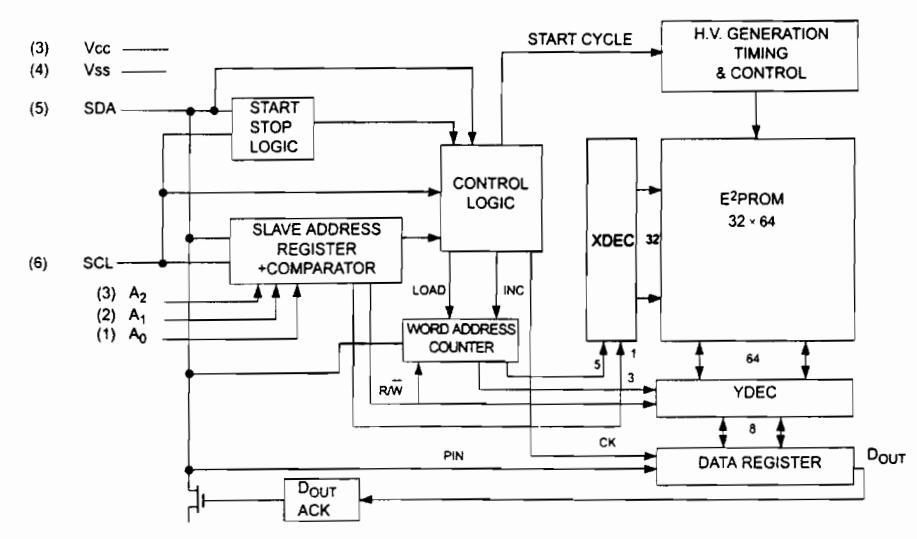
KM6264 BCS-10L:S-RAM(MEMORY)
a.GENERAL DESCRIPTION
The KM6264B/BL/BL-L is a 65,536-bit high-speed Static Random Access Memory orgranized as 8,192 words by 8 bit. The device is fabricated using Samsung's advanced CMOS process. The KM6264B/BL/BL-L has an output enable input for precise control of the data outputs. It also has chip select inputs for the minimum current power down mode. The KM6264B/BL/BL-L has been designed for high speed and low power applications. It is particularly well suited for battery back-up non-volatile memory applications.
b.FEATURES
- Fast Access Time: 70,100,120, ns (max.)
- Low Power Dissipation
- Standby (CMOS): 10µ W (typ.) L-Version 5µ W (typ.) LL-Version
- Operating: 55mW/MHz (max.)
- Single 5V±10% Power Supply
- TTL compatible inputs and outputs
- Fully Static Operation
- No clock or refresh required
- Three State Output
- Low Data Retention Voltage: 2V (min.)
- JEDEC Standard pin Configuration KM6264B/BL/BL-L: 28-pin DIP (600 mil) KM6264BS/BLS/BLS-L: 28-pin DIP (300 mil) KM6264BG/BLG/BLG-L: 28-pin SOP (330 mil)
c.PIN CONFIGURATION AND NAMES
| A0-A12 | Address inputs |
|---|---|
| WE | Write enable |
| CS1,CS2 | Chip select |
| OE | Output enable |
| 1/01-1/08 | Data input/Output |
| Vcc | +5V power supply |
| Vss | Ground |
24 -
d.Recommanded operating conditions (ta=0℃ to 70℃) * Note: VIL(min)=-3.0V for ≤ 50ns pulse.
| Parameter | Symbol | Min. | Тур. | Max. | Unit |
|---|---|---|---|---|---|
| Supply voltage | Vcc | 4.5 | 5.0 | 5.5 | V |
| Ground | Vss | 0 | 0 | 0 | V |
| Input high voltage | ViH | 2.2 | — | Vcc+0.3 | V |
| Input low voltage | VIL | -0.3 | 0.8 | V |
For Service Manuals Contact MAURITRON TECHNICAL SERVICES 8 Cherry Tree Rd, Chinnor Oxon OX9 4QY fel: 01844-351694 Fax:- 01844-352554
Email:- enquiries@mauritron.co.uk


INTEGRATED VIP AND TELETEXT(IVT)
a.GENERAL DESCRIPTION
The integrated VIP and Teletext(IVT) is a teletext decoder (contained within a single chip package) for decoding 625-line based World System Teletext tramsmissions. The teletext decoder hardware is based on the Enhanced Computer Controlled Teletext (ECCT) device (SAA5243) with some additional features; existing ECCT software remains compatible. The Video Input Processor (VIP) section of the device uses new mixed analogue and digital designs for the Data Slicer and the Display Clock Phase Locked Loop functions. As a result the number of
c.PINNING DESCRIPTION
external components is greatly reduced and no critical or adjustable components are required.
Features
- Complete teletext decoder in single 48-pin DIL package
- Single +5V power supply
- Digital Data Slicer and Display Clock Phase Locked Loop reduce peripheral components to a minimum
- Both video and scan related synchronization modes are supported
- 4/8 page acquisition system is software compatible with ECCT
- RGB interface to standard color decoder ICs, push pull output drive; requires only 2 external resistors
- Data capture performance comparable with SAA5231 (VIP2)
- Software compatibility with ECCT maintained
- Interfaces with 8K×8-bit static RAM
- Optional storage of packet 24 in the display memory
- Packet 8/30/2 mapped to a different extension chapter as an aid for VCR programming applications
b.QUICK REFERENCE DATA
| Parameter | Symbol | Min. | Тур. | Max. | Unit |
|---|---|---|---|---|---|
| Supply voltage | VDD | 4.5 | 5 | 5.5 | V |
| Supply current | l dd l | 60 | 120 | mA | |
| Sync amplitude | Vsyn | 0.1 | 0.3 | 0.6 | V |
| Video amplitude | Vvid | 0.7 | 1 | 1.4 | V |
| Crystal frequency | fXTAL | 27 | MHz | ||
| Operating ambient temperature range | Tamb | -20 | — | +70 | r |
| Pin | Name | Description |
|---|---|---|
| 1 | VDDD | +5V supply to the digital sections of the device. |
| 2 | OSCOUT | 27MHz crystal oscillator output. |
| 3 | OSCIN | 27MHz crystal oscillator input. |
| 4 | OSCGND | Crystal oscillator ground, 0V. |
| 5 | VSSA | Analogue ground, 0V. |
| 6 | REF+ | Positive reference voltage for the ADC. If necessary, the pin should be connected to |
| | | analogue +5Vvia decoupling components. | |
| 7 | BLANK | Video black level storage pin, connected to analogud ground via a 100nFcapacitor. |
| 8 | CVBS | Composite video input pin. A positive-going 1V peak-to-peak input is required, |
| connected via a 100nF capacitor. | ||
| 9 | Iref | Reference current input pin, connected to analogue ground via a 27ko resistor. |
| 10 | VDDA | +5V supply to the analogue sections of the device. |
| 11 | POL | STTV/LFB/FFB polarity select pin. |
| 12 | STTV/LFB | Sync to TV output pin/line flyback input pin, function controlled by an internal register |
| bit. | ||
| 13 | VCR/FFB | PLL time constant switch/field flyback input pin, function control by an internal register |
| bit. | ||
| 14 | VSSD | Connected to VSSD for normal operation. |
| 15 | R | Dot rate character output of the RED colour information. |
| 16 | G | Dot rate character output of the GREEN colour information. |
| 17 | В | Dot rate character output of the BLUE colour information. |
| 18 | RGBREF | DC voltage to define the output high level on the RGB pins. |
| 19 | BLAN | Dot rate fast blanking output. HIGH for text and LOW for picture. |
- 25 -
| Pin | Name | Description |
|---|---|---|
| 20 | COR | Programmable output to provide contrast reduction of the TV picture for mixed text |
| 21 | ODD/EVEN |
and picture displays or when viewing newsflash/subtitle pages.
25Hz output synchronized with the CVBS input's field sync pulses to produce a noninter laced display by adjustment of the vertical deflection currents. |
| 22 | Y | Dot rate character output of teletext foreground colour information. Open drain output. |
| 23 | SCL | Serial clock input for I 2 C-bus. It can still be driven HIGH during power-down of the device. |
| 24 | SDA | Serial data port for the I 2 C-bus. Open drain output. It can still be driven HIGH during power-down of the device. |
| 25 | VSSD | Digital ground, 0V. |
| 26-33 | D0-D7 | Data lines for the page RAM. |
| 34-46 | A0-A12 | Address lines for the page RAM. |
| 47 | OE | Output enable to the page RAM. |
| 48 | WE | Write enable to the page RAM. |
d. IVT BLOCK DIAGRAM

- 26-
8 TROUBLESHOOTING CHARTS
NO POWER · Chart 1

NO RASTER (SOUND OK) : Chart 3


NO SOUND (Picture OK) : Chart 6
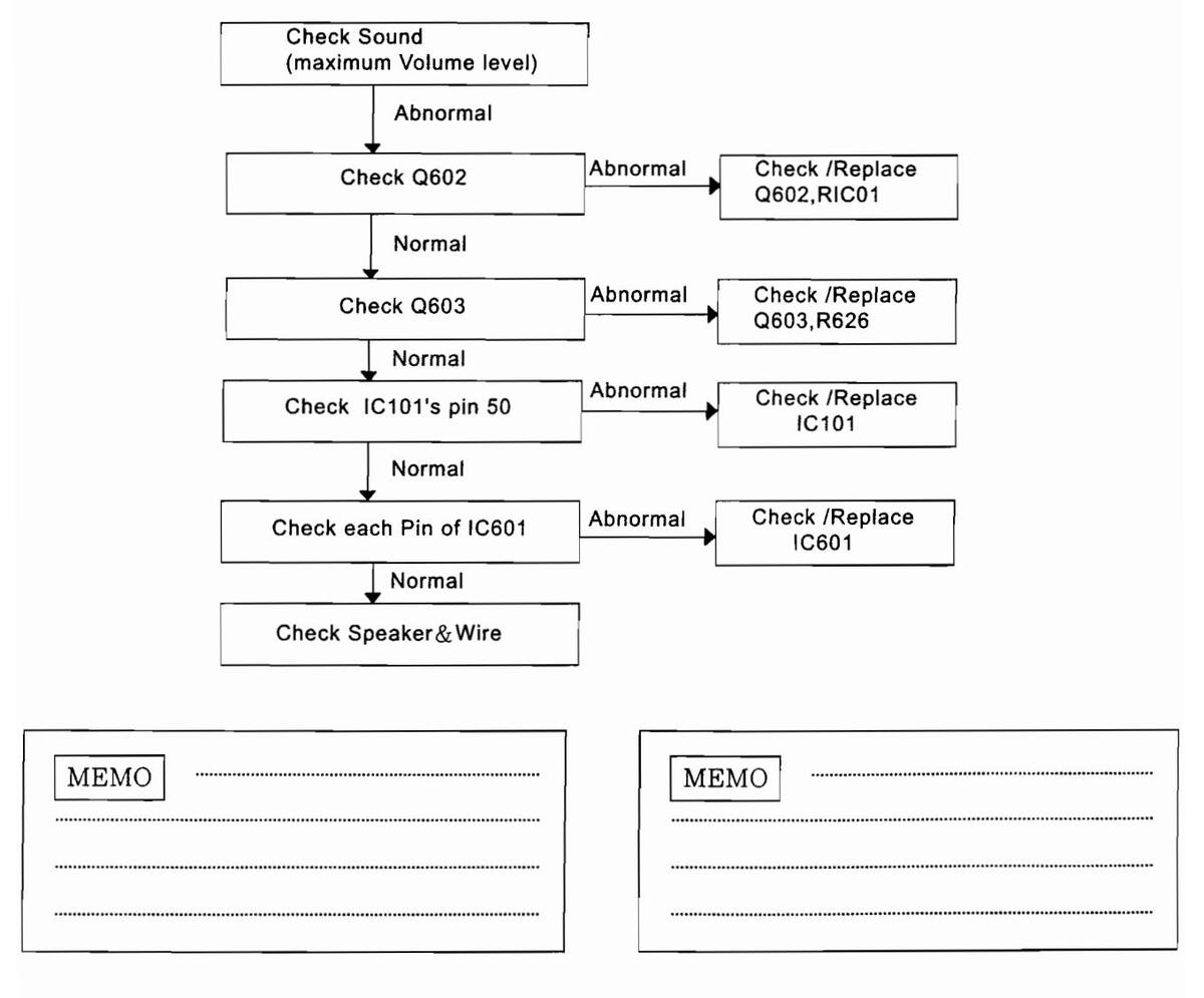
6. NO TTX(THE TV OPERATING IS O.K)

| MEMO | MEMO |
|---|---|
| For Service Manuals Contact | |
|
MAURITRON TECHNICAL SERVICES
B'Chairy Trea Hd, Chinnor |
|
|
Tel:-01844-851694-Fax:-01844-352554
Email:-enquiries@mauriton.co.uk |
|
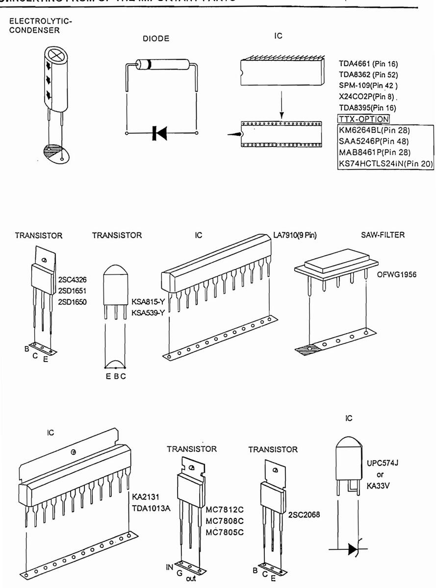
9.INSERTING FROM OF THE IMPORTANT PARTS
- 31 -
10. CHASSIS REPLACEMENT PARTS LIST
| ABBREVIATIONS | : |
CC
CE CFS CK CQ CS |
C-CERAMIC
C-ELECTROLYTIC C-M,POLYESTER C-CERAMIC,HK C-POLYPROPYLENE,POLYESTE C-TANTALIUM,SOLID |
RC
RD RF RP RS |
R-COMPOSITION
R-CARBON R-FUSIBLE R-METAL,FILM R-CEMENT WIRE R-METAL,OXIDE |
|---|
NOTE : The items with "*" are usually out of stock since they are seldom required for the routine service. There may be some anticipated delay when you order these items.
S.N.A. = Service Not Available , L/C = Local Purchase
The components identified by mark '**' are critical for safety. Replace only with Supplier part number specified.
When indicating parts by location number, Please include the PWB names ( PWB = Printed Writing Board )
|
Loc
No |
Supplier
Parts No. |
Specification |
Loc
No |
Supplier
Parts No. |
Specification |
|---|---|---|---|---|---|
|
A S S Y - P W
*3X30-01720Y03 |
B, MAIN
O CI3352X/TSECX |
R 306
R 307 R 308 R 309 |
31018-377-159
31018-177-513 31018-177-183 31018-377-271 |
RD 1/2T 1.5R-J
RD 1/8T 51K-J RD 1/8T 18K-J RD 1/2T 270-J |
|
|
PWB
MR001 |
33004-157-411
RESISTORS 31018-377-122 |
P68SC-M
|
R310
R311 R312 R313 R401 |
31018-177-153
31018-177-224 31018-177-223 31018-377-105 31018-177-153 |
RD 1/8T 15K-J
RD 1/8T 220K-J RD 1/8T 22K-J RD 1/2T 1M-J RD 1/8T 15K-J |
|
MR002
R100 R106 R112 |
31018-377-122
31018-177-682 31018-177-391 31018-177-682 |
RD 1/2T 1.2K-J
RD 1/8T 6.8K-J RD 1/8T 390-J RD 1/8T 6.8K-J |
R402
R404 R407 R408 |
31018-177-273
31018-177-332 31018-377-124 31018-177-101 |
RD 1/8T 27K-J
RD 1/8T 3 3K-J RD 1/2T 120K-J RD 1/2T 100-J |
|
R113
R114 R115 R116 R117 |
31018-177-333
31018-177-104 31018-177-104 31018-177-561 31018-177-562 |
RD 1/8T 33K-J
RD 1/8T 100K-J RD 1/8T 100K-J RD 1/8T 560-J RD 1/8T 5.6K-J |
R410
R411 ★★R412 ★★R414 ★★R414 |
31018-377-680
31059-002-010 31059-427-151 31049-101-350 |
RD 1/27 2/0-J
RD 1/27 68-J RF 1/2P 1-J RF 1P 150-J RS 1P 1K-J |
|
R122
R123 R124 R201 R202 |
31018-177-473
31018-177-473 31018-177-104 31018-177-102 31018-177-181 |
RD 1/8T 47K-J
RD 1/8T 47K-J RD 1/8T 100K-J RD 1/8T 1K-J RD 1/8T 180-J |
R416
R417 **R418 R420 |
31018-377-473
31018-377-563 31059-002-010 31018-177-824 |
RD 1/2T 47K-J
RD 1/2T 56K-J RF 1/2P 1-J RD 1/8T 820K-J |
|
R203
R204 R205 R207 R208 |
31018-177-131
31018-177-109 31018-177-102 31018-177-622 31018-177-472 |
RD 1/8T 130-J
RD 1/8T 1-J RD 1/8T 1R-J RD 1/8T 6.2K-J RD 1/8T 4.7K-J |
R500
R501 R502 R503 R504 |
31018-177-473
31018-177-562 31018-177-103 31018-177-104 31018-177-561 |
RD 1/8T 47K-J
RD 1/8T 5.6K-J RD 1/8T 10K-J RD 1/8T 100K-J RD 1/8T 560-J |
|
**R209
**R210 R211 R212 |
31048-361-001
31049-375-194 31018-177-750 31018-177-750 |
RM 1/2T 1K-G
RM 1/2T 190K-F RD 1/8T 75-J RD 1/8T 75-J RD 1/8T 75-J |
R505
R506 R507 R510 |
31018-177-101
31018-177-101 31018-177-101 31018-177-750 |
RD 1/8T 100-J RD 1/8T 75-J PD 1/8T 75-J |
|
R214
R215 R216 R220 R303 |
31018-177-273
31018-177-102 31018-177-181 31018-177-331 |
RD 1/8T 27R-J
RD 1/8T 1R-J RD 1/8T 180-J RD 1/8T 330-J |
R511
R512 R516 R518 R519 |
31018-177-750
31018-177-103 31018-177-470 31018-177-470 |
RD 1/8T 75-J
RD 1/8T 10K-J RD 1/8T 47-J RD 1/8T 75-J |
|
R304
R305 |
31018-377-681
31018-177-203 |
RD 1/2T 680-J
RD 1/8T 20K-J |
R520
R608 R609 |
31018-177-154
31018-177-562 31018-177-562 |
RD 1/8T 150R-J
RD 1/8T 5.6R-J RD 1/8T 5.6R-J |
For Service Manuals Contact MAURITRON TECHNICAL SERVICES 8 Cherry Tree Rd, Chinnor Oxon OX9 4QY Tel:- 01844-351694 Fax:- 01844-352554 Email:- enquiries@mauritron.co.uk
|
Loc
No |
Supplier Specification
Parts No. |
Loc
No |
Supplier
Parts No. |
Specification |
|---|---|---|---|---|
|
R61
R61 R61 R61 |
0 31018-177-101 RD 1/8T 100-J
4 31018-177-432 RD 1/8T 4.3K-J 5 31018-177-203 RD 1/8T 20K-J 6 31018-177-224 RD 1/8T 220K-J |
**R918
**R919 **R920 |
31046-567-183
31046-567-183 31046-567-183 |
RS 2T 18K-J(AUTO)
RS 2T 18K-J(AUTO) RS 2T 18K-J(AUTO) |
|
R61
R61 R61 R62 |
7 31018-177-562 RD 1/8T 5.6K-J
8 31018-377-479 RD 1/2T 4.7-J 9 31018-177-122 RD 1/8T 1.2K-J 2 31018-177-102 RD 1/8T 1K-J 2 31018-177-102 RD 1/8T 1K-J |
**R921
**R922 **R923 **R924 **R925 |
31028-327-182
31028-327-182 31028-327-182 31059-003-100 31059-003-100 |
RC 1/2T 1.8K-J
RC 1/2T 1.8K-J RC 1/2T 1.8K-J RF 1P 1-K RF 1P 1-K |
|
R62
R62 R63 |
3 31018-177-103 RD 1/8T 10K-J 4 31018-177-103 RD 1/8T 10K-J 6 31018-177-562 RD 1/8T 5.6K-J 7 31018-177-121 RD 1/8T 120-J 0 31018-177-223 RD 1/8T 120-J |
RR01
RR02 RR04 RR05 |
31018-177-332
31018-177-103 31018-177-153 31018-177-103 |
RD 1/8T 3.3K-J
RD 1/8T 10K-J RD 1/8T 15K-J RD 1/8T 10K-J RD 1/8T 10K-J |
|
R64
R64 |
0 31018-177-202 RD 1781 2K-J
1 31018-377-470 RD 1/2T 47-J 2 31018-177-203 RD 1/8T 20R-J |
RR07 |
31018-177-103
31018-177-472 31018-177-103 |
RD 1/81 10K-J
RD 1/8T 4.7K-J RD 1/8T 10K-J |
|
R70
R70 R70 R70 |
3 31018-177-273 RD 1/8T 27K-J
4 31018-177-103 RD 1/8T 10K-J 5 31018-177-124 RD 1/8T 120K-J 6 31018-177-202 RD 1/8T 2K-J |
RR09
RR10 RR11 |
31018-177-202
31018-177-202 31018-177-162 |
RD 1/8T 2K-J
RD 1/8T 2K-J RD 1/8T 2K-J RD 1/8T 1.6K-J |
|
R70
R70 R71 **R80 |
7 31018-177-753 RD 1/8T 75K-J
9 31018-177-202 RD 1/8T 2K-J 0 31018-177-223 RD 1/8T 22K-J 2 31039-787-479 RW 10H 4.7-J 2 31018-177-223 RD 1/8T 270K J |
RR12
RR13 RR14 RR15 RR16 |
31018-177-823
31018-177-203 31018-177-103 31018-177-752 31018-177-821 |
RD 1/8T 82K-J
RD 1/8T 20K-J RD 1/8T 10K-J RD 1/8T 7.5K-J RD 1/8T 820-J |
| R80 |
5 31018-377-274 RD 1/21 270K-J
4 31018-377-274 RD 1/2T 270K-J 5 31048-547-104 RS 2N 100K-1 |
RR17
RR18 RR24 |
31018-177-202
31018-177-102 31018-177-102 |
RD 1/8T 2K-J
RD 1/8T 1K-J RD 1/8T 1K-J |
|
**R80
R80 **R81 |
7 31049-537-110 RS 2M 110-J
8 31018-377-103 RD 1/2T 10K-J 1 31049-315-030 RS 2P 18K-J |
RR25
RR26 |
31018-177-102
31018-177-102 |
RD 1/8T 1K-J
RD 1/8T 1K-J RD 1/8T 1K-J |
|
R81
R81 R81 R81 |
2 31039-427-279 RW 3P 2.7-J
4 31018-277-339 RD 1/4T 3.3-J 5 31018-377-101 RD 1/2T 100-J 6 31018-377-331 RD 1/2T 330-J 7 21056-002 130 RE 1/2R 0 47-F |
RR27
RR28 RR29 RR30 RR37 |
31018-177-102
31018-177-102 31018-177-103 31018-177-102 31018-177-181 |
RD 1/8T 1K-J
RD 1/8T 1K-J RD 1/8T 10K-J RD 1/8T 1K-J RD 1/8T 1K-J RD 1/8T 180-J |
| **R81 | 8 31049-527-399 RS 2P 3.9-J |
RR38
RR39 RR40 |
31018-177-222
31018-177-223 31018-177-181 |
RD 1/8T 2.2K-J
RD 1/8T 22K-J RD 1/8T 180-J |
|
R82
**R82 **R82 |
31018-177-101 RD 1/8T 100-J
31049-315-390 RS 2P 15K-J 4 31049-315-101 RS 2P 100-J |
RR42
RR43 |
31018-177-181
31018-177-102 |
RD 1/8T 180-J
RD 1/8T 1K-J |
|
**R82
**R83 **R83 R90 |
6 31059-002-010 RF 1/2P 1-J
0 31028-328-475 RC 1/2T 4.7M-K 1 31028-328-475 RC 1/2T 4.7M-K 1 31018-177-152 RD 1/8T 1.5K-J 2 31018-177-152 RD 1/8T 1.5K-J |
RR44
RR45 RR46 RR47 RR48 |
31018-177-102
31018-177-101 31018-177-101 31018-177-101 31018-177-101 |
RD 1/8T 100-J
RD 1/8T 100-J RD 1/8T 100-J RD 1/8T 100-J RD 1/8T 100-J |
| R90 |
3 31018-177-152 RD 1/8T 1.5K-J
4 31018-177-751 RD 1/8T 750-J |
RR50
RR51 RR52 |
31018-177-202
31018-177-682 31018-177-222 |
RD 1/8T 2K-J
RD 1/8T 6.8K-J RD 1/8T 2.2K-J |
|
R90
R90 R90 |
5 31018-177-751 RD 1/8T 750-J
6 31018-177-751 RD 1/8T 750-J 7 31018-177-102 RD 1/8T 1K-J 8 21018-177-102 RD 1/8T 1K-J |
RR53
RR54 |
31018-177-222
31018-177-222 31018-177-222 |
RD 1/8T 2.2K-J
RD 1/8T 2.2K-J RD 1/8T 2.2K-J |
|
R90
R90 R91 R91 |
9 31018-177-102 RD 1/8T 1K-J
1 31018-177-102 RD 1/8T 1K-J 3 31018-177-102 RD 1/8T 1K-J 3 31018-177-151 RD 1/8T 150-J |
RR55
RR57 RR58 RR59 RR61 |
31018-177-221
31018-177-470 31018-177-470 31018-177-223 31018-177-681 |
RD 1/8T 220-J
RD 1/8T 47-J RD 1/8T 22K-J RD 1/8T 22K-J RD 1/8T 680-J |
|
R91
R91 |
4 31018-177-561 RD 1/8T 560-J
5 31018-377-104 RD 1/2T 100K-J |
VARIABLE RESIS | STORS | |
|
R91
R91 |
6 31018-377-104 RD 1/2T 100R-J
7 31018-377-104 RD 1/2T 100R-J |
VR101
VR201 |
31249-128-001
31249-128-008 |
ENV-DJA AO3 B14
ENV-DJA AO3 B54 |
|
Loc
No |
Supplier
Parts No. |
Specification |
Loc
No |
Supplier
Parts No. |
Specification |
|---|---|---|---|---|---|
|
VR301
VR303 |
31249-128-004 | ENV-DJA AO3 B13 | C420 | 31607-401-500 | CEO4W TAPG 16V 470M-M |
|
VR304
VR304 VR401 VR801 |
31249-128-001
31249-128-001 31249-128-003 |
ENV-DJA AO3 B23
ENV-DJA AO3 B14 ENV-DJA AO3 B23 |
C422
C423 C424 C425 |
31417-106-090
31417-106-090 31417-106-090 31607-401-710 |
CK45 TAPG B 500V 471-K
CK45 TAPG B 500V 471-K CK45 TAPG B 500V 471-K CED4W TAPG 25V 470M-M CC45(T) CH 50V 180-L |
|
VR902
VR903 |
31249-128-004
31249-128-004 31249-128-004 |
ENV-DJA AO3 B13
ENV-DJA AO3 B13 ENV-DJA AO3 B13 |
C503 | 31507-127-016 | ECQ B1 H 472J F3 |
|
VR904
VR905 VRR41 |
31249-128-004
31249-128-004 31249-128-005 |
ENV-DJA AO3 B13
ENV-DJA AO3 B13 ENV-DJA AO3 B53 |
C504
C505 C506 C507 |
31507-127-012
31507-127-012 31507-127-012 31607-402-250 |
EVOBI H 104J-F3
EVOBI H 104J-F3 EVOBI H 104J-F3 CE04W TAPG 50V 10M |
| CAPACITORS |
C508
C509 |
31607-402-250
31507-127-012 |
CEO4W TAPG 50V 10M
EVOB1 H 104J-F3 |
||
|
C102
C104 C109 C110 |
31407-101-140
31417-109-220 31607-402-220 31507-127-012 |
CC45(T) SL 50V 120-J
CK45 TAPG F 50V 223-Z CE04W TAPG 50V 2.2M FV0BL H 1041-F3 |
C510
C511 C512 |
31507-127-012
31507-127-012 31507-127-012 31507-127-008 |
EVOBI H 104J-F3
EVOBI H 104J-F3 ECO B1 H 223J F3 |
| Č115 | 31507-127-012 | EVQB1 H 104J-F3 |
C513
C515 |
31607-401-460
31417-104-400 |
CEO4W TAPG 16V 47M
CK45 TAPG B 50V 102-K |
|
C116
C117 C118 C119 |
31507-127-016
31607-402-220 31607-402-250 31607-401-500 |
ECQ B1 H 472J F3
CE04W TAPG 50V 2.2M CE04W TAPG 50V 10M CE04W TAPG 16V 470M-M |
C516
C521 C550 |
31417-104-400
31607-401-430 31607-401-500 |
CK45 TAPG B 50V 102-K
CE04W TAPG 25V 10M CE04W TAPG 16V 470M-M |
| ČĺŻÓ | 31607-902-250 | CEO4W TAPG 50V 0.22M |
C609
C610 |
31607-803-730
31607-803-730 |
CEO4W TAPG 50V 4.7M-NP
CEO4W TAPG 50V 4.7M-NP |
|
C122
C124 C125 |
31607-402-070
31607-902-250 31607-402-250 |
CEO4W TAPG 35V 22M
CEO4W TAPG 50V 0.22M CEO4W TAPG 50V 10M |
C612
C613 C615 |
31507-127-012
31507-127-006 31507-127-003 |
EVQBI H 104J-F3
ECO B1 H 103J F3 ECO B1 H 332J F3 |
|
C201
C202 |
31507-127-010
31607-402-250 |
CEO4W TAPG 50V 10M |
C616
C617 |
31607-402-210
31607-401-770 |
CEO4W TAPG 50V 1M
CEO4W TAPG 25V 2200M-M |
|
C203
C204 C205 |
31507-127-010
31507-127-012 31507-127-012 |
ECQ B1H 473J F3
EVQB1 H 104J-F3 EVOB1 H 104J-F3 |
C618
C620 C621 |
31607-803-280
31607-402-110 31507-127-002 |
CEO4W TAPG 50V 1U-M(NP)
CEO4W TAPG 35V 220M-M ECQ B1H 222J F3 |
|
C206
C207 |
31607-401-500
31507-127-012 |
CEO4W TAPG 16V 470M-M
EVQB1 H 104J-F3 |
C623 | 31607-402-250 | CEO4W TAPG 50V 10M |
|
C208
**C209 |
31607-401-840
31517-003-020 31507-127-003 |
CE04W TAPG 10V 100M-M
CFS922M TAPG 400V 104-J FC0 B1 H 3321 F3 |
C625
C626 C627 |
31407-105-260
31407-105-660 31407-105-660 |
CC45(T) CH 50V 470-J
CC45(T) CH 50V 101-J CC45(T) CH 50V 101-J CC45(T) CH 50V 101-J |
|
C303
C304 |
31507-127-011
31507-127-012 |
ECO B1H 683J F3
EVQB1 H 104J-F3 |
C628 | 31407-105-660 | CC45(T) CH 50V 101-J |
| C305 | 31609-904-332 |
CE04W 25V 3300u
CE04W TAPG 50V 2.2M |
C630
C633 C701 |
31407-105-260
31507-127-016 31607-401-430 |
ECO B1 H 472J F3
CEO4W TAPG 25V 10M |
|
C307
C309 |
31607-402-290
31507-127-014 |
CEO4W TAPG SOV 100M-M
ECO B1 H 272J F3 |
Č702 | 31607-401-430 | CE04W TAPG 25V 10M |
| C310 | 31507-127-022 | ECQ B1 H 513J F3 |
(800
**(801 **(802 |
31507-137-005
31569-204-190 31569-204-190 |
250V 0.47M/KNB 1530
250V 0.47M/KNB 1530 |
|
C312
C401 |
31507-127-016
31607-402-210 |
ECO B1 H 472J F3
GEO4W TAPG 50V 1M |
C803
C804 |
31467-502-220
31467-502-220 |
CK45P TAPC E250V 222-Z
CK45P TAPC E250V 222-Z |
|
C402
C403 |
31507-127-016
31417-109-220 |
ECQ B1 H 4/2J F3
CR45 TAPG F 50V 223-Z |
C805
C806 |
31467-502-220
31467-502-220 |
CK45P TAPG E250V 222-Z
CK45P TAPG E250V 222-Z |
|
C404
C405 C409 |
31417-104-490
31507-127-000 31507-137-013 |
CR45 TAPG D 50V 272-M
ECQ B1 H 102J F3 ECQ-B 1 103J F3 |
**C807
C808 C810 |
31519-010-000
31417-767-331 31417-901-400 |
CF922M 630V 0.022M-J
CK45(T) B2KV 331-K CK45(T) B2KV 561-K |
|
**C411
C414 |
31519-400-005
31607-402-710 |
CFS 922M 1600V 0.0072-J
CE04W TAPG 35V 1000M-M |
C811 | 31417-901-400 |
CK45(T) B2KV 561-K
CK45P F400V 332-M(T4KV) |
|
C416
**C417 C418 C419 |
31607-403-070
31509-335-130 31607-403-450 31607-401-720 |
CEO4W TAPG 100V 68M-M
CQ922M 200V 0.36-J CEO4W TAPG 250V 1M CEO4W TAPG 25V 1000M-M |
C836
C836 C837 C838 |
31417-109-140
31607-401-340 31607-401-710 |
CK45 TAPG F 50V 103-Z
CE04W TAPG 10V 1000M-M CED4W TAPG 25V 470M-M |
For Service Manuals Contact MAURITRON TECHNICAL SERVICES 8 Cherry Tree Rd, Chinnor Oxon OX9 4QY Tel: 01844-351694 Fax:- 01844-352554 Email:- enquiries@mauritron.co.uk
- 34 -
|
Loc
No |
Supplier Specification
Parts No. |
Loc
No |
Supplier
Parts No. |
Specification |
|---|---|---|---|---|
|
C851
C852 C853 C854 C854 |
31609-403-780 CEO4W 400V 100M-M(LIG)
31607-401-500 CEO4W TAPG 16V 470M-M 31607-403-250 CEO4W TAPG 160V 100M-M 31607-403-230 CEO4W TAPG 160V 33M-M 31607-401-720 CEO4W TAPG 25V 1000M-M |
0201
0202 0703 0602 |
32137-301-720
32137-301-720 32137-401-530 32137-401-530 |
KSC 815-Y(TAPG)
KSC 815-Y(TAPG) KSA 539-Y(TAPG) KSA 539-Y(TAPG) |
|
C856
C857 C858 C859 C859 C901 |
31607-401-720 CEO4W TAPG 25V 1000M-M
31607-402-250 CEO4W TAPG 50V 10M 31607-401-140 CEO4W TAPG 6.3V 1000M-M 31607-401-710 CED4W TAPG 25V 470M-M 31407-105-120 CC45(T) CH 50V 121-J |
0905
R012 0903 0902 0901 |
32137-401-530
32137-401-530 32139-410-006 32139-410-006 32139-410-006 |
KSA 539-Y(TAPG)
KSA 539-Y(TAPG) KTC2068 KTC2068 KTC2068 |
|
C902
C903 C904 C905 C906 |
31407-105-120 CC45(T) CH 50V 121-J
31407-105-120 CC45(T) CH 50V 121-J 31417-104-250 CK45 TAPG B 50V 471-K 31417-104-250 CK45 TAPG B 50V 471-K 31417-104-250 CK45 TAPG B 50V 471-K |
D102
D201 D301 D302 |
D10DES
32167-406-480 32167-201-070 32167-406-480 32167-201-140 22167-201-140 |
1N4148 TAPG
1N4003 TAPG 1N4148 TAPG KF105S KF105S |
|
C907
C908 RC01 RC02 RC03 |
31417-767-102 CK45(T) B2KV 102-K
31607-403-450 CE04W TAPG 250V 1M 31507-127-001 ECQ B1 H 152J F3 31507-127-025 EVQ-V1H 334J Z3 31507-127-025 EVQ-V1H 334J Z3 |
D401
D402 D403 D404 D405 D410 |
32167-201-140 1
32167-208-510 32167-201-070 32167-201-070 32167-406-480 |
KF105S
ERB 43-04 TAPG 1N4003 TAPG 1N4003 TAPG 1N4148 TAPG |
|
RC04
RC05 RC06 RC07 RC08 |
31607-402-250 CEO4W TAPG 50V 10M
31607-402-250 CEO4W TAPG 50V 10M 31607-402-250 CEO4W TAPG 50V 10M 31607-402-250 CEO4W TAPG 50V 10M 31507-127-002 ECQ B1H 222J F3 |
D411
D505 D506 D507 D508 |
32167-406-480
32167-406-480 32167-406-480 32167-406-480 32167-406-480 |
1N4148 TAPG
1N4148 TAPG 1N4148 TAPG 1N4148 TAPG 1N4148 TAPG 1N4148 TAPG |
|
RC09
RC10 RC12 RC13 RC13 RC15 |
31407-057-330 CC45(T) CH 50V 330-J
31607-401-450 CE04W TAPG 16V 33M 31607-401-470 CE04W TAPG 16V 100M VENT 31417-344-104 CK45 TAPG F 50V 104-Z 31607-401-470 CE04W TAPG 16V 100M VENT |
D513
D601 D704 D705 D801 |
32167-406-480
32167-406-480 32167-406-480 32167-406-480 32167-406-480 32167-201-180 |
1N4148 TAPG
1N4148 TAPG 1N4148 TAPG 1N4148 TAPG 1N4148 TAPG M100J(TAPG) |
|
RC16
RC17 RC21 RCT01 |
31607-401-470 CEO4W TAPG 16V 100M VENT
31407-105-700 CG45(T) CH 50V 151-J 31417-104-400 CK45 TAPG B 50V 102-K 31497-009-340 EXF-FP4 331MDV(5P 331) I C |
D802
D803 D804 D805 D806 |
32167-201-180
32167-201-180 32167-201-180 32167-201-180 32169-301-670 32167-207-120 |
M100J(TAPG)
M100J(TAPG) M100J(TAPG) RH—2F 1R5GU41(TAPG) |
|
**D2824
IC101 IC501 **IC801 **IC803 |
32119-101-360 KA 33V(TAPG)
32119-110-052 TDA8362 32119-110-089 TDA4661 32119-910-017 SDH-209B 32119-401-110 MC7805C (AUTO) |
D807
D808 D809 D810 D811 |
32167-207-120
32167-406-480 32167-406-480 32167-406-480 32167-406-480 32167-406-480 |
1R5GU41(TAPG)
1N4148 TAPG 1N4148 TAPG 1N4148 TAPG 1N4148 TAPG 1N4148 TAPG |
|
RICO1
RICO2 RICO3 |
32109-110-072 SPM109B/PCA84C640P-051
32109-210-023 X24C02P 32119-110-061 KIA7033P(T) TRANSISTORS |
DZ501
DZ825 RD01 RD03 RD04 |
32167-406-080 |
32167-441-009 | 32167-406-480 32167-406-480 32167-406-480 32167-406-480 |
MTZ 5.1B
MTZ7.5C 1N4148 TAPG 1N4148 TAPG 1N4148 TAPG 1N4148 TAPG |
|
**0401
**0803 **0802 R010 R005 |
32137-301-560 KSC 2331-Y(TAPG)
32137-301-560 KSC 2331-Y(TAPG) 32137-301-560 KSC 2331-Y(TAPG) 32137-301-560 KSC 2331-Y(TAPG) 32137-301-720 KSC 815-Y(TAPG) 32137-301-720 KSC 815-Y(TAPG) |
RDO6
RDO8 RDO9 RD10 RD11 |
32167-406-480
32167-406-480 32167-406-480 32167-406-480 32167-406-480 32167-406-480 |
1N4148 TAPG
1N4148 TAPG 1N4148 TAPG 1N4148 TAPG 1N4148 TAPG 1N4148 TAPG |
|
0705
R009 Q601 R011 R011 |
32137-301-720 KSC 815-Y(TAPG)
32137-301-720 KSC 815-Y(TAPG) 32137-301-720 KSC 815-Y(TAPG) 32137-301-720 KSC 815-Y(TAPG) 32137-301-720 KSC 815-Y(TAPG) 32137-301-720 KSC 815-Y(TAPG) |
RD14
RDZ01 RDZ02 RDZ03 RDZ04 |
32167-101-130
32167-401-800 32167-401-800 32167-401-800 32167-401-800 32167-401-800 |
1K34A (TAPG)
EQA02-06A/MTZ5.6B(TAPG) EQA02-06A/MTZ5.6B(TAPG) EQA02-06A/MTZ5.6B(TAPG) EQA02-06A/MTZ5.6B(TAPG) |
| Q704 | 32137-301-720 KSC 815-Y(TAPG) | RDZ05 | 32167-401-800 | EQA02-06A/MTZ5.6B(TAPG) |
|
Loc
No |
Supplier Specification
Parts No. |
Loc Supplier Specification
No Parts No. |
|---|---|---|
| POSISTOR | MISCELLANEOUS | |
| ** P801 | 32189-609-390 2C18R | CN201 33345-108-310 67094-003(SEP) |
| MODULE REMOCON |
CN202 3334/-114-820 YW025-04 (AUTO, NO TUBE)
CN44 33124-205-007 4P 6-12.5-14MM |
|
| **PR01 | 32199-411-002 SR-5CP |
CN601 33345-108-310 6/094-003(SEP)
CN602 33058-302-016 B3XB3/F/400 |
| LED | CN801 33124-205-003 2P 10MM | |
| **LD01 | 32309-110-230 DS2 (DL-ILR)/SL-5R |
CN802 33124-205-003 2P 10MM
CN901 33058-332-016 B6XB6/F/400 |
| COILS |
CN902 33058-302-016 B3XB3/F/400
CNR01 33058-312-012 B4XB4/F/300 |
|
|
D-COIL
L102 L103 L201 L403 |
32479-029-100 9.2RT70L 940(DOU)
32427-904-918 AL02-1R0K 32427-904-922 AL02-5R6K 32427-805-330 5.6UH-M 32429-833-020 6.8MH-K |
EJ01 33333-510-120 HSJ0807-01-010
F801 33167-001-001 PFC 5000-0202 L400 34047-019-060 3.5X6X1.0 L804 34047-019-060 3.5X6X1.0 L807 34047-019-060 3.5X6X1.0 |
|
L404
L503 L601 L801 L803 |
32449-712-010 K-10/195UH
32427-904-922 AL02-5R6K 32427-805-450 12UH-K TAPG 32429-633-090 39MHX2(U) 32429-226-080 1UH-K |
SGJ01 33136-103-030 HXC-1510-01-300A(R) SW101 33609-101-025 RPT 2104-21 SW102 33598-001-001 JTR-1104 SW103 33598-001-002 JTR-1105 SW801 33529-402-006 ESB-99835V/ESB-99832V |
| L805 | 32429-014-070 100UH-K | ASSY-H/S VERT(SOUND) |
| L901 | 32429-823-010 3300H-K | *3H82-00070Y000 35684-116-210, TDA1013A |
| RLÖI | 32427-904-924 AL02-100K(10UH) | **IC602 32119-201-070 TDA1013A/N4 |
|
RLO2
RLO3 |
32427-904-924 AL02-100K(10UH)
32427-904-924 AL02-100K(10UH) |
SGREW 37158-230-061 2S-3X6 FE FZY |
| RL04 | 32427-904-924 AL02-100R(100H) | ASSY-H/S VERT(HORI) |
| TRANS | *3H82-00170Y000 14"2SD1650 | |
|
T101
**T401 **T801 |
32717-513-800 38.9MHZ(S-60)
32849-070-002 7.3MH/105UH 32899-002-450 P:90-260,S:125/18V(ER42) |
**
Q402 32159-210-002 2SD1650 YD
H/SINK 35684-118-110 SPC-1 T1.0 FT2 SCREW 37158-230-101 2S-3X10 FE FZY WASHE 37334-105-910 SPC-1 T1.0 FZY-1 |
| TRANS FLYBACK | ASSY-H/S VERT | |
| **1444 | 32839-132-310 FGM-2014FL | *3H82-00170Y003 35684-118-110 KA2131 |
| IC301 32119-102-300 KA 2131 | ||
| ~~V999A | 33339-063-610 HF-22.3A |
H/SINK 35684-118-110 SPG-1 11.0 FTZ
HOLD/W 36604-134-510 NYLON 66 VO NTR |
| ******* |
10NER
24510-200-020 TECC2085V414P |
SCREW 37148-330-081 25-3X8 FE F21
SCREW 37158-230-061 2S-3X6 FE F2Y |
| **10001 | S4J19-700-020 IEGG2963VA14B | ASSY-H/S POWER |
| 7101 | 34529-700-012 TSE5321 | *3H83-00380Y000 2SC4236,35684-121-710 |
|
Z202
Z602 |
34527-460-008 TPS6.0MBTF21
34527-460-007 SFE6.0MBTF21 |
**
0801 32159-210-007 2SC4236
H/SINK 35684-121-710 A1050S-H14 T2.0(2SC4236) SCREW 37158-230-101 2S-3X10 FE FZY |
| CRYSTALS | ASSY-H/S POWER | |
|
RX01
X501 |
34539-001-000 10MHZ
34539-011-010 HC-49/U 4.433619MHZ |
*3H84-00020Y000 MC7812,CKD |
| FUSE | **1C402 32119-901-110 MC7812C (AUTO) | |
| ** F801 | 34709-084-730 FST 250V 3.15A 20MM |
H/SINK 35684-118-330 A6063 EXTR BLK H30
SCREW 37158-230-061 2S-3X6 FE FZY |
For Service Manuals Contact MAURITRON TECHNICAL SERVICES 8 Cherry Tree Rd, Chinnor Oxon OX9 4QY Tel: 01844-351694 Fax:- 01844-352554 Email:- enquiries@mauritron.co.uk
|
ASSY-H/S TR
*3884-000201007 35684-118-330,NC7808C **10802 32119-401-304 NC7808C(AUTO) HSINK 35684-118-330 A663 EXFR BLK H30 SCREW 37158-230-61 23-336 FF F2T A S S Y - H O L D E R , S P K *3893-533521020 CB3352X, LEM/C 33058-003-012 S3220/F300 SFK 34209-200-20 OSF148RA, 88, 33 HOLLS 36601-238-820 FFS VO BLK #066 GRILL 37712-117-410 SFC-17 0.7 #066 A S S Y - P O W E R , C O R D P0W/C 33054-001-714 CTBS-2F/7.SF48LK-H0U HOLDS 36601-238-820 FFS VO BLK #066 GRILL 37712-117-410 SFC-17 0.7 #066 A S S Y - C R T DY 32439-400-003 DSE-1422EL(1) CT 34099-027-010 JH-225 SF-DY 3641-101-911 NOPFKNE VO BLK A S S Y - A C C E S S O R Y TRANK 32759-113-010 R300-R75, MATCH W/BALUN R0W/A 3150-720-002 UL 620MH CAROVA 38124-123-110 MAT PAPER 120 S6850 FFS-83833-109-151 BDPF T0.015 230X400 |
Loc Supplier Specification
No Parts No. |
Loc Supplier Specification
No Parts No. |
|---|---|---|
|
*3H84-00020Y007 35684-118-330,MC7808C
**CG02 32119-001-30A MC7808C(AUTO) H/SINK 3564-118-330,M605 XXTR BLK H30 SCREW 37158-230-061 ZS-336 FE FZY A S S Y - T R A N S H I T T E R *3F14-00032-140 TM32,RM109,29,E,SS A S S Y - H O L D E R , S P K *1H33-53352F020 CB3352X, LEAD/C 33058-003-012 S322W/F/300 SFK 34209-200-020 SF148RA,8K,3W TBLOS 36601-2308202 N V0 BLK M656,352 HCLLS 37601-2308202 N V0 BLK M656,352 HCLLS 37601-2308202 N V0 BLK M656,352 HCLLS 37012-117401 SFC-1 T0.7 #066 A S S Y - P O W E R , C O R D POW/C 33054-801-114 GTFS-2F/7.SF4BLK-H0U HCLD/C 3605-11143 OF SC-1 T0.7 #066 A S S Y - C R T DY 32439-400-003 DSE-1422EL(1) CT 34099-227-010 JH-225 SP-DY 36614-101-911 NE0PERNE VO BLK A S S Y - A C C E S S O R Y Text. Stoff-220-020 N/UL 520MM COM 00540Y Te 01844-3064 Fac UF44-32254 Emit-equine@fmailto.01.4 SVG/N 38134-372-010 ATT PAPER 120 P685C PE-BAG 38633-108-191 HDFE T0.015 230X400 |
ASSY-H/S TR | |
**C022 32119-001-304 MC7806C(AUT0) |
*3H84-00020Y007 35684-118-330,MC7808C | |
|
A S S Y - T R A N S M I T T E R
*3F14-00032-140 TM32,RM109,29,E,SS A S S Y - H O L D E R , S P K *3B93-53352V020 CB3352X, LEAD/C 31058-003-012 S3274/7400 S700,27 35601-238-820 HPS Y0 BLK #066 GRILL 37712-117-410 SPC-1 T0.7 #066 A S S Y - P O W E R , C O R D POW/C 33054-801-114 CTBS-2F/7.5F+BLK-HOU HOLD/C 36603-111-310 P.P Y0 BLK (NEW) A S S Y - C R T DY 32439-400-003 D5E-1422HL(1) CY 34099-027-010 JH-225 SP-DY 36614-101-311 NGOPERNE Y0 BLK A S S Y - A C C E S S O R Y TRAW/M 32759-113-010 R300-875, MATCH W/BALUN ROD/A 33659-220-020 VUL 820M Y0 J124-137-610 ART PAPER 120 P68SC PE-BAG 38653-108-191 HDPE T0.015 230X400 |
**IC802 32119-401-304 MC7808C(AUT0) H/SINK 35684-118-330 A6063 EXTR BLK H30 SCREW 37158-230-061 2S-3X6 FE FZY |
|
|
*3F14-00032-140 TM32.RM109.29,E,SS
A S S Y - H O L D E R , S P K *3093-53352Y020 CB3352X, LEAD/C 33058-003-012 S322A/F/300 SFK 3420-200-C00 OF1ABAR.98,30 MOL/C 36601-238-820 FS Y0 BLK 4066 GRILL 37712-117-410 SPC-1 T0.7 #066 A S S Y - P O W E R , C O R D POV/C 35034-801-118 (TTS-7F/7 SFHELR-HOU BOL/C 36603-111-310 P.P YO BLK (NEW) A S S Y - C R T DY 32439-400-003 DSE-1422HL(1) CY 3409-027-010 JH-225 SP-DY 36814-101-911 NEOPREVE V0 BLK A S S Y - A C C E S S O R Y TRAV.M 3259-213-010 R300-R75. NARCE W/BALUNR GROW 3124-1327-010 KHT PAPER 100 J K 33134-337-010 KHT PAPER 100 J K 33134-337-010 KHT PAPER 100 J K 33134-337-010 KHT PAPER 100 J K 33134-337-010 KHT PAPER 100 J K 33134-337-010 KHT PAPER 100 J K 33134-337-010 KHT PAPER 100 J K 33134-337-010 KHT PAPER 100 J K 33134-337-010 KHT PAPER 100 J K 33134-337-010 KHT PAPER 100 J K 33134-337-010 KHT PAPER 100 J K 33134-337-010 KHT PAPER 100 J K 33134-337-010 KHT PAPER 100 J K 33134-337-010 KHT PAPER 100 J K 33134-337-010 KHT PAPER 100 J K 33134-337-010 KHT PAPER 100 J K 33134-337-010 KHT PAPER 100 J K 33134-337-010 KHT PAPER 100 J K 33134-337-010 KHT PAPER 100 J K 33134-337-010 KHT PAPER 100 J K 33134-337-010 KHT PAPER 100 J K 33134-337-010 KHT PAPER 100 J K 33134-337-010 KHT PAPER 100 J K 33134-337-010 KHT PAPER 100 J K 33134-337-010 KHT PAPER 100 J K 33134-337-010 KHT PAPER 100 J K 33134-337-010 KHT PAPER 100 J K 33134-337-010 KHT PAPER 100 J K 33134-337-010 KHT PAPER 100 J K 33134-337-010 KHT PAPER 100 J K 33134-337-010 KHT PAPER 100 J K 33134-337-010 KHT PAPER 100 J K 33134-337-010 KHT PAPER 100 J K 33134-337-010 KHT PAPER 100 J K 33134-337-010 KHT PAPER 100 J K 33134-337-010 KHT PAPER 100 J K 33134-337-010 KHT PAPER 100 J K 33134-337-010 KHT PAPER 100 J K 33134-337-010 KHT PAPER 100 J K 33134-337-010 KHT PAPER 100 J K 33134-337-010 KHT PAPER 100 J K 33134-337-010 KHT PAPER 100 J K 33134-337-010 KHT PAPER 100 J K 33134-337-010 KHT PAPER 100 J K 33134-337-010 KHT PAPER 100 J K 33134-337-010 KHT PAPER 100 J K 33134-337-010 KHT PAPER 100 J K 33134-337-010 KHT PAPER 1 |
ASSY-TRANSMITTER | |
|
A S S Y - H O L D E R , S P K
*3393-53352Y020 CB3352X, LEAD/C 33058-003-012 S322/F/300 SYK 73209-200-203 OS 70 BLK 4006 3332 HOL/Y 36601-233-820 PS V0 BLK 4006 GRILL 37712-117-410 SPC-1 T0.7 #066 A S S Y - P O W E R , C O R D POW/C 33054-801-114 CTBS-2F/7.5F4BLK-HOU HOL/C 36051-1113-10 P.F V0 BLK (NEW) A S S Y - C R T DY 32439-400-003 DSE-1422EL(1) CY 3409-027-010 JH-225 SP-DY 36814-101-911 NEOPRENE V0 BLK A S S Y - A C C E S S O R Y TRAN/M 32759-113-010 R300-R75.MATCE W/BALUN R0D/A 3507-220-020 R300-R75.MATCE W/BALUN R0D/A 3507-220-020 R300-R75.MATCE W/BALUN R0D/A 3507-220-020 R300-R75.MATCE W/BALUN R0D/A 35134-375-610 WTL 620M7 SGV/W 38134-375-610 WTL 620M7 J C J 3439-420-101 ART PAPER 100 J C J 3434-375-610 WTL 620M7 SGV/W 38134-375-610 WTL 620M7 SGV/W 38134-376-610 WTL 620M7 J C J 38653-106-191 HDPE T0.015 Z30X400 |
*3F14-00032-140 TM32,RM109,29,E,SS | |
|
*3893-53352Y020 CB3352X,
LEAD/C 33058-003-012 S332M/F/300 SYR 3409-200-20 S9F1488A.8R,3W ROLD/S 36601-2380820 PS YO BLX #066 GRILL 37712-117-410 SPC-1 T0.7 #066 A S S Y - P O W E R , C O R D POW/C 33054-601-114 (TBS-2F/7.5F+BLR-BOU GOLD/C 36603-111-310 P.P YO BLK (NEW) A S S Y - C R T DY 32439-400-003 DSE-1422HL(1) CY 34099-027-010 JH=225 SP-DY 3614-010-811 NEOPRENE YO BLK A S S Y - A C C E S S O R Y TRANYM 32759-113-010 R300-R75 MATCH W/BALUN ROD/A 3509-227-00 WIT PAPER 200 SVC/A 38134-379-00 WIT PAPER 200 SVC/A 38134-372-010 ART PAPER 200 SVC/A 38134-372-010 ART PAPER 200 SVC/A 38134-327-010 ART PAPER 200 SVC/A 38134-327-010 ART PAPER 200 SVC/A 38134-372-010 ART PAPER 200 SVC/A 38134-372-010 ART PAPER 200 SVC/A 38134-372-010 ART PAPER 200 SVC/A 38134-372-010 ART PAPER 200 SVC/A 38134-372-010 ART PAPER 200 SVC/A 38134-372-010 ART PAPER 200 SVC/A 38134-372-010 ART PAPER 200 SVC/A 38134-372-010 ART PAPER 200 SVC/A 38134-372-010 ART PAPER 200 SVC/A 38134-372-010 ART PAPER 200 SVC/A 38134-372-010 ART PAPER 200 SVC/A 38134-372-010 ART PAPER 200 SVC/A 38134-372-010 ART PAPER 200 SVC/A 38134-372-010 ART PAPER 200 SVC/A 38134-372-010 ART PAPER 200 SVC/A 38134-372-010 ART PAPER 200 SVC/A 38134-372-010 ART PAPER 200 SVC/A 38134-372-010 ART PAPER 200 SVC/A 38134-372-010 ART PAPER 200 SVC/A 38134-372-010 ART PAPER 200 SVC/A 38134-372-010 ART PAPER 200 SVC/A 38134-372-010 ART PAPER 200 SVC/A 38134-372-010 ART PAPER 200 SVC/A 38134-372-010 ART PAPER 200 SVC/A 38134-372-010 ART PAPER 200 SVC/A 38134-372-010 ART PAPER 200 SVC/A 38134-372-010 ART PAPER 200 SVC/A 38134-372-010 ART PAPER 200 SVC/A 38134-372-010 ART PAPER 200 SVC/A 38134-372-010 ART PAPER 200 SVC/A 38134-372-010 ART PAPER 200 SVC/A 38134-372-010 ART PAPER 200 SVC/A 38134-372-010 ART PAPER 200 SVC/A 38134-202 SVC/A 38134-202 SVC/A 38134-202 SVC/A 38134-202 SVC/A 38134-202 SVC/A 38134-202 SVC/A 38134-202 SVC/A 3814 SVC/A 3814 SVC/A 3814 SVC/A 3814 SVC/A 3814 SVC/A 3814 SVC/A 3814 SVC/A 3814 SVC/A 3 |
ASSY-HOLDER, SPK | |
|
L L&D/C 33058-003-012 S3320/F/300
SPR 4 3209-200-20 S9F1488.8 8, 34 HOL/X 36601-238-020 PS YO BLK #066 GRILL 37712-117-410 SPC-1 T0.7 #066 A S S Y - P O W E R , C O R D POW/C 33054-801-114 GTBS-2F/7.5F+BLR-BOU HOLD/C 36603-111-310 P.P VO BLK (NEW) A S S Y - C R T DY 32439-400-003 DSE-1422HL(1) CY 34099-027-010 JH-225 SP-DY 36414-010-911 NEOPRENE YO BLK A S S Y - A C C E S S O R Y TRANYM 32759-113-010 R300-875 MATCH W/BALUN R0D/A 33124-122-010 ART PAPER 120 P685C PE-BAG 38653-108-191 HDPE T0.015 230X400 |
*3⊞93-53352¥020 CB3352X, | |
|
A S S Y - P O W E R , C O R D
POW/C 33054-801-114 CTBS-2F/7.5F+BLR-HOU HOLD/C 36603-111-310 P.P VO BLR (NEW) A S S Y - C R T DY 32439-400-003 DSE-1422HL(1) CY 34099-027-010 H=225 SP-DY 36814-101-911 NEOPREVE VO BLR A S S Y - A C C E S S O R Y TRAN/M 32759-113-010 R300-R75,MATCH W/BALUN ROD/A 34509-220-020 V/UL 620MM CARD/W 38124-132-610 WHT PAPER 120 P68SC PE-BAC 38653-108-191 HDPE T0.015 230X400 |
LEAD/C 33058-003-012 S3ä2ü/F/300
SPK 34209-200-020 05F14BRA,8R,3W HOLD/S 36601-238D820 PS VO BLK #066 3352 HOLD/S 36601-238-820 HIPS VO BLK #066 GRILL 37712-117-410 SPC-1 T0.7 #066 |
|
| POW/C 33054=01-114 GTBS-2F/7.5F+BLR-HOU WOLD/C 3603-111-310 P.P. Y0 BLR (NEW) A S S Y - C R T Dy 32439-400-003 DSE-1422HL(1) CY 32439-400-010 JH-225 DY SP-DY 36814-101-911 NEOPRANE VO BLK A S S Y - A C C E S S O R Y TRAN/N 32759-113-010 R300-R75, MATCH W/BALUN ROD/A 34509-220-020 N/UL 620MM SEUK CARD/W 38124-132-610 WHT PAPER 120 P68SC PE-BAG 38653-108-191 HDPE T0.015 230X400 | ASSY-POWER, CORD | |
|
A S S Y - C R T
DY 32439-400-003 DSE-1422HL(1) CY 33099-027-010 JH-225 SP-DY 36814-101-911 NEOPRENE VO BLK A S S Y - A C C E S S O R Y TRAN/M 32759-113-010 R300-R75, MATCH W/BALUN ROD/A 36509-220-020 N/UL 620MM CARD/W 38124-132-610 WHT PAPER 220(S) SEUR SYC/N 38134-479-010 ART PAPER 120 P68SC PE-BAC 38653-108-191 HDPE T0.015 Z30X400 |
POW/C 33054-801-114 GTBS-2F/7.5F+BLK-HOU
HOLD/C 36603-111-310 P.P VO BLK (NEW) |
|
| DY 32439-400-003 DSE-1422HL(1) CY 34099-027-010 JH-225 SP-DY 3614-101-911 NEOPREVE VO BLK A S S Y - A C C E S S O R Y Email: enquines@mauntron.co.uk TRAN/M 32759-113-010 R300-R75, MATCH W/BALUN ROD/A 34509-220-020 N/UL 620MM CARD/W 38124-1379-010 ART PAPER 120 (S) SEUK SYC/N 38134-379-010 ART PAPER 120 P68SC PE-BAG 38653-108-191 HDPE T0.015 230X400 | ASSY-CRT |
8 Cherry Tree Rd, Chinnor
Oxon OX9 4QY |
|
A S S Y - A C C E S S O R Y
TRAN/M 32759-113-010 R300-R75, MATCH W/BALUN R0D/A 34509-220-020 N/UL 620MM CARD/W 38124-132-610 WHT PAPER 220(S) SEUK SYC/N 38134-329-010 ART PAPER 120 I/B 38134-425-110 ART PAPER 120 P68SC PE-BAG 38653-108-191 HDPE T0.015 230X400 |
DY 32439-400-003 DSE-1422HL(1)
CY 34099-027-010 JH-225 SP-DY 36814-101-911 NEOPRENE VO BLK |
Tel:- 01844-351694 Fax:- 01844-352554
Email:- enquiries@mauritron.co.uk |
|
TRAN/M 32759-113-010 R300-R75.MATCH W/BALUN
ROD/A 34509-220-020 N/UL 620MM CARD/W 38124-132-610 WHT PAPER 220(S) SEUK SVC/N 38134-79-010 ART PAPER 100 I/B 38134-425-110 ART PAPER 120 P68SC PE-BAG 38653-108-191 HDPE T0.015 230X400 |
A S S Y – A C C E S S O R Y | |
|
TRAN/M 32759-113-010 R300-R75, MATCH W/BALUN
ROD/A 34509-220-020 N/UL 620MM CARD/W 38124-132-610 WHT PAPER 220(S) SEUK SVC/N 38134-379-010 ART PAPER 100 I/B 38134-425-110 ART PAPER 120 P68SC PE-BAG 38653-108-191 HDPE T0.015 230X400 |
||
11. EXPLODED-VIEW

CI3352X/TSECX
The items with "*" are usually out of stock since they are seldom required for the routine service. There may be some anticipated delay when you order these items. *** S.N.A = SERVICE NOT AVAILABLE. ***
| NO | CODE NO | DESCRIPTION | SPECIFICATION | Q'TY | NO | CODE NO | DESCRIPTION | SPECIFICATION | Q'TY |
|---|---|---|---|---|---|---|---|---|---|
| 1 | 37712-117-410 | GRILLE-WOOFER,L | SPC-1 T0.5 4R #066 | 1 | 33 | 34209-200-020 | SPEAKER-GENERAL | 05F 14BRA 8R 3W | 2 |
| 2 | 36601-238-820 | HOLDER-SPEAKER | HIPS VO BLK | 1 | 34 | *3H83-00380Y000 | ASSY-H/S,POWER | 2SC 4236 | 1 |
| 3 | *3Y90-33520-060 | ASSY-CABINET, FRONT | HIPS BLK #066 | 1 | 35 | 33529-402-006 | SWITCH-PUSH, POWER | ESB-99835V/ESB-99832V | 1 |
| 36001-665-010 | CABINET-FRONT | HIPS HB BLK #066 | 1 | 36 | 33609-101-025 | SWITCH-TACT | KPT-2104-21 | 1 | |
| 4 | 36023-118-810 | STOPPER-PCB | HIPS HB NTR | 1 | 37 | 37624-621-510 | KNOB-SUB,MASTER | ABS HB BLK | 1 |
| 5 | 37333-101-020 | WASHER-GUM,CRT | NATURAL RUBBER | 4 | 38 | 32309-110-230 | LED | DS2/SL-5R | 1 |
| 6 | LOCAL-PURCHASE | CRT-COLOR | 1 | 39 | 32196-411-002 | REMOCON-MODULE | SR-5CP(R) | 1 | |
| 7 | 36635-001-910 | CLAMPER-D,COIL | NYLON 6.6 | 2 | 40 | 33598-001-001 | SWITCH-RUBBER | JTR-1104 | 1 |
| 8 | 37124-100-810 | SCREW-CRT | 5X30 RH+W/S AUTO | 4 | 41 | 33058-003-012 | LEAD-CONNECTOR,ASSY | S3(2)/F/300 | |
| 9 | 33479-029-100 | COIL-DEGAUSSING | 9.2RT70L | 1 | 42 | 37712-117-410 | GRILLE-SPEAKER,R | SPC-1 T0.5 4R #066 | 1 |
| 10 | 32439-400-003 | DEFL-YOKE | DSE 1442 HL | 1 1 | 43 | 36601-238-820 | HOLDER-SPEAKER | HIPS VO BLK #066 | 1 |
| 11 | 34099-027-010 | MAGNET-CONVERGENCE | JH-225 | 1 | 44 | 38013-116-710 | INDICATOR-LED | ACRYL CLEAR | 1 |
| 12 | 36814-101-911 | SPACER-DY | NEOPRENE VO BLK | 1 | 45 | 36674-139-810 | SPRING-COIL | SUS P10.5 | 4 |
| 13 | 37148-540-152 | SCREW-TAP,RH | 2S-4X15 FE FZW | 6 | 46 | 37623-158-310 | KNOB-POWER,MASTER | ABS HB BLK #066 | 1 |
| 14 | 36001-666-020 | CABINET-BACK | HIPS VO BLK | 1 | 47 | 37623-158-530 | KNOB-CHANNEL | ABS HB BLK | 1 |
| 15 | 36633-101-610 | CLAMPER-CORD | P.E HB BLK | 1 | 48 | 36674-137-820 | SPRING-COIL | SUS P10.5 | 4 |
| 16 | 38112-000-000 | LABEL-RATTING | TETRONE PAPER | 1 | 49 | 37623-158-430 | KNOB-VOLUME | ABS HB BLK | 1 |
| 17 | 33054-801-114 | POWER-CORD | KKD-419C KLCE-2F | 1 | 50 | 37653-125-550 | WINDOW REMOTE | PC GE LEXAN | 1 1 |
| 18 | 33598-001-002 | SWITCH-RUBBER | JTR-1105 | 1 | 51 | 36698-100-110 | CATCH-PUSH,DOOR | KIFUCO LA701 | 1 |
| 19 | *3X30-01720Y030 |
ASSY-PWB MAIN
|
CI3352X/TSECX | 1 | 52 | 38024-178-010 | BADGE-BRAND | AL-FORGING | 1 |
| 33004-157-411 |
PWB-MAIN
|
330X245X1.6T | 1 | 53 | 38093-121-110 | PVC-CONTROL | PVC SHEET TO.3 BLK | 1 | |
| 20 | *3H82-00070Y000 | ASSY-H/S,VERT(SOUND) | TDA1013A | 1 | 54 | 37642-140-050 | DOOR-CONTROL | HIPS HB BLK #066 | 1 |
| 21 | *3H84-00020Y000 | ASSY-H/S,TR | MC7812C | 1 | 55 | *3H82-00170Y000 | ASSY-H/S,VERT(HOR1) | 14" 2SD1650 | 1 |
| 22 | 34519-700-020 | TUNER | TECC-2985VA14B | 1 | |||||
| 23 | 33136-103-030 | RECEPTACLE-PERI | HXC-1510-01-300A(R) | 1 | |||||
| 24 | 36604-134-510 | HOLDER-WIRE | NYLON 66 VO NTR | 1 | |||||
| 25 | 37158-530-081 | SCREW-TAP,RH | 2S-3X8 FE FZY | 1 | |||||
| 26 | 32859-152-510 | TRANS-FLYBACK | FCM-2014FL | 1 | |||||
| 27 | 36603-111-310 | HOLDER-CORD | P.P VO BLK(NEW) | 1 | |||||
| 28 | 37148-540-152 | SCREW-TAP,RH | 2S-4X15 FE FZW | 1 | quini 1516 | ||||
| 29 | *3H84-00020Y007 | ASSY-H/S,TR | MC7808C | 1 |
es of CHar
@ TXX |
||||
| 30 | *3H82-00170Y003 | ASSY-H/S,VERT | KA2131 | 1 | mau 9 40, | ||||
| 31 | 36633-101-910 | CLAMPER-FBT,C | ABS VO GRY | 1 | |||||
| 32 | 37148-530-101 | SCREW-TAP,RH | 2S-3X12 FE FZY | 1 |
ontaci
Innor 14-3525 1.00.uk |
(097 B 0-040-0 6 BLK12V 8 G P CNO
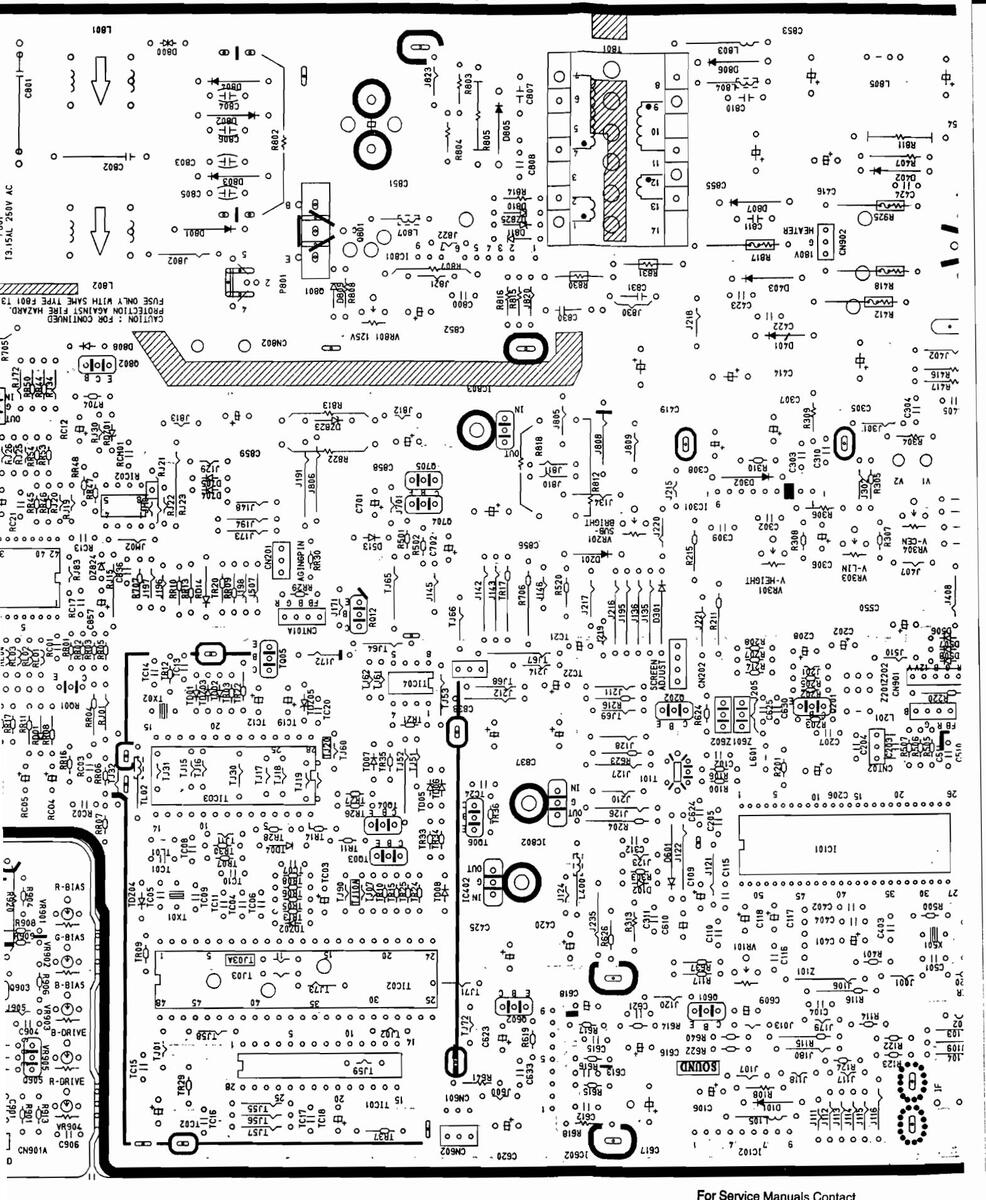
For Service Manuals Contact MAURITRON TECHNICAL SERVICES 8 Cherry Tree Rd, Chinnor Oxon OX9 4QY Tel: 01844-351694 Fax: 01844-352554 Email: enquiries@mauritron.co.uk


SCHEMATIC DIAGRAM
CHASSIS: P68SC(N), (M), (H) MODEL: CK(B. X. I)505 I X (T) BOARD NAME: MAIN SYSTEM: PAL/SECAM-B. G & D. K (PAL-I)
For Service Manuals Contact MAURITRON TECHNICAL SERVICES 8 Cherry Tree Rd, Chinnor Oxon OX9 4QY Tel: 01844-351684 Fax:- 01844-352554 Email:- enquiries@mauritron.co.uk
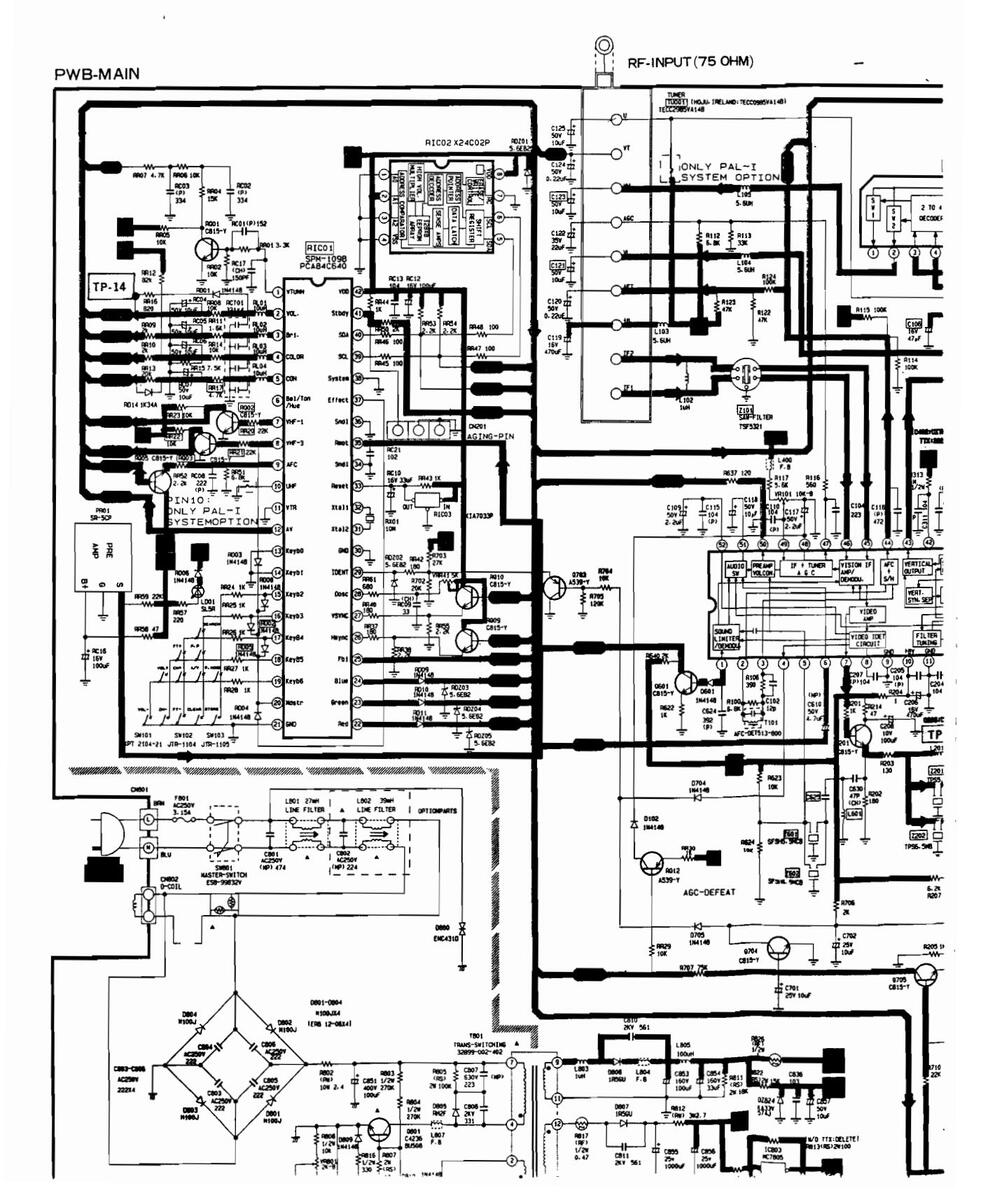
For Service Manuals Contact MAURITRON TECHNICAL SERVICES 8 Cherry Tree Rd, Chinnor Oxon OX9 4QY Tel:- 01844-351694 Fax:- 01844-35255 Email:- enquiries@mauritron.co.uk

For Service Manuals Contact MAURITRON TECHNICAL SERVICES 8 Cherry Tree Rd, Chinnor Oxon OX9 4QY Tel: 01844-351694 Fax:- 01844-352554 Email:- enquiries@mauritron.co.uk

For Service Manuals Contact MAURITRON TECHNICAL SERVICES 8 Cherry Tree Rd, Chinnor Oxon OX9 4QY Tel:- 01844-351694 Fax:- 01844-352554 Emeil:- enguiries@mauritron.co.uk


TESTPOINT WAVEFROM
| TP-1 | TP-2 | TP-3 TP-4 | TP-5 |
|---|---|---|---|
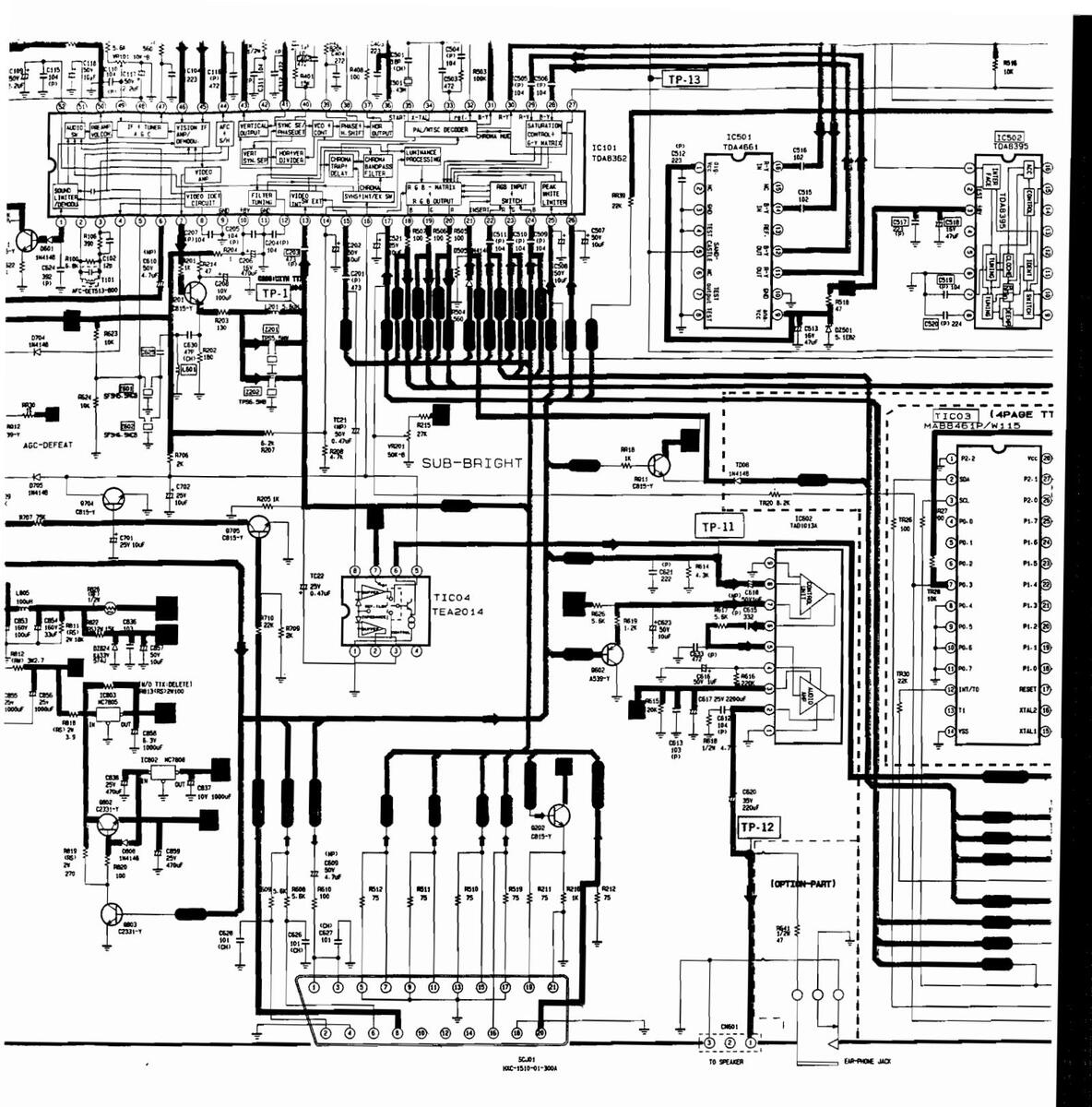
| TP-4 | TP-5 | TP-6 | TP-7 | TP-8 |
|---|---|---|---|---|

_____ EAR-PHONE JACK
TP-8
| TF | »-9 | ) | ; ° ~ | |||||||
|---|---|---|---|---|---|---|---|---|---|---|
| į۳, | í. | - | 21 | ·str | 1. | 2 1 ,29 | ſ | |||
|
1
1 1 1 1 1 1 1 |
|
|||||||||
| þ | 2 | |||||||||
| Ē | •••• |
|
1 | - | ||||||
| ľ | ||||||||||
| | |
••••• |
ł | ||||||||
| I |
| TP-10 | ||||||
|---|---|---|---|---|---|---|
| 21-488- | 1992 28 41 | |||||
|
)
|
l | |||||
| NT | Z | h | ||||
| . 1 | ¥ | |||||


For Service Manuals Contact MAURITRON TECHNICAL SERVICES 8 Cherry Tree Rd, Chinnor Oxon OX9 4QY Tel: 01844-351694 Fax:- 01844-352554 Email:- enquiries@mauritron.co.uk

| TP-10 | TP-11 | TP-12 | TP-13 | TP-14 |
|---|---|---|---|---|
| 2 - 21 - 477 - 1992 - 24 - 41 | ||||
 Service manual & schematics")


 Loading...