

Page 1

TFT-LCD MONITOR
CN15V*
Manual
SERVICE
TFT-LCD MONITOR CONTENTS
EXIT MENUAUTO EXIT MENUAUTO
1. Precautions
2. Product Specifications
3. Disassembly & Reassembly
4. Troubleshooting
5. Exploded View & Parts List
6. Electrical Parts List
7. Block Diagram
8. Wiring Diagram
9. Schematic Diagrams
10. Panel Description
CN15VS
CN15VO
EXIT MENUAUTO EXIT MENUAUTO
Page 2
1-1-1 Warnings
1. For continued safety, do not attempt to modify the
circuit board.
2. Disconnect the AC power and DC Power Jack
before servicing.
3. When the chassis is operating, semiconductor
heatsinks are potential shock hazards.
1-1-2 Servicing the LCD Monitor
1. When servicing the LCD Monitor, remove the static
charge by connecting a 10k ohm resistor in series
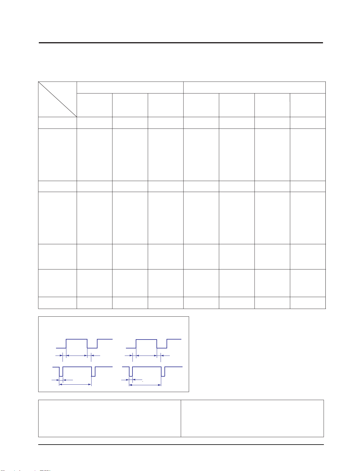
with an insulated wire (such as a test probe)
between the chassis and the anode lead.
(Disconnect the AC line cord from the AC outlet.)
2. It is essential that service technicians have an
accurate voltage meter available at all times. Check
the calibration of this meter periodically.
1-1-3 Fire and Shock Hazard
Before returning the monitor to the user, perform the
following safety checks:
1. Inspect each lead dress to make certain that the
leads are not pinched or that hardware is not
lodged between the chassis and other metal parts in
the monitor.
2. Inspect all protective devices such as nonmetallic
control knobs, insulating materials, cabinet backs,
adjustment and compartment covers or shields,
isolation resistor-capacitor networks, mechanical
insulators, etc.
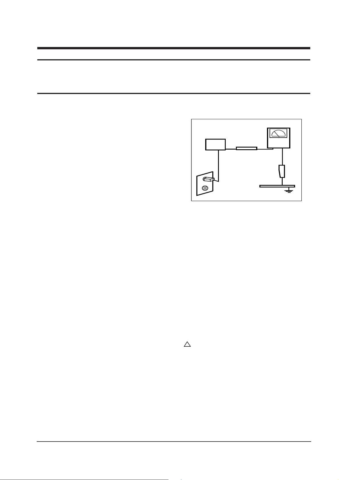
3. Leakage Current Hot Check (Figure 1-1): WARNING:
Do not use an isolation transformer during this test.
Use a leakage current tester or a metering system
that complies with American National Standards
Institute (ANSI C101.1, Leakage Current for
Appliances), and Underwriters Laboratories (UL
Publication UL1410, 59.7).
Figure 1-1. Leakage Current Test Circuit
4. With the unit completely reassembled, plug the AC
line cord directly into a 120V AC outlet. With the
unit’s AC switch first in the ON position and then
OFF, measure the current between a known earth
ground (metal water pipe, conduit, etc.) and all
exposed metal parts, including: metal cabinets,
screwheads and control shafts. The current
measured should not exceed 0.5 milliamp. Reverse
the power-plug prongs in the AC outlet and repeat
the test.
1-1-4 Product Safety Notices
Some electrical and mechanical parts have special
safety-related characteristics which are often not
evident from visual inspection. The protection they give
may not be obtained by replacing them with
components rated for higher voltage, wattage, etc. Parts
that have special safety characteristics are identified by
on schematics and parts lists. A substitute
replacement that does not have the same safety
characteristics as the recommended replacement part
might create shock, fire and / or other hazards. Product
safety is under review continuously and new
instructions are issued whenever appropriate.
CN15V* 1-1
1 Precautions
Follow these safety, servicing and ESD precautions to prevent damage and to protect against potential hazards such as
electrical shock.
1-1 Safety Precautions
DEVICE
UNDER
TEST
TEST ALL
EXPOSED METAL
SURFACES
(READING SHOULD
NOT BE ABOVE 0.5mA)
LEAKAGE
CURRENT
TESTER
2-WIRE CORD
ALSO TEST WITH
PLUG REVERSED
(USING AC ADAPTER
PLUG AS REQUIRED)
EARTH
GROUND
!
Page 3

2 Product Specifications
2-1 Specifications
LCD Panel TFT-LCD panel, RGB vertical stripe, normaly white, 15-Inch viewable,
0.297 (H) x 0.297 (V) pixel pitch
Scanning Frequency Horizontal : 30 kHz ~ 61 kHz (Referring to Timing chart, Page 2-3, 2-4)
Vertical : 50 Hz ~ 75 Hz (Referring to Timing chart, Page 2-3, 2-4)
Display Colors 16,003,008 colors
Maximum Resolution Horizontal : 1024 Pixels Vertical : 768 Pixels
Input Video Signal Analog, 0.714 Vp-p ± 5% positive at 75 Ω, internally terminated
Input Sync Signal Type: Seperate H/V sync, Composite H/V, Sync-on-Green, automatic synchronization
without external switch of sync type
Level: TTL level
Maximum Pixel Clock rate 80 MHz
Active Display Horizontal/Vertical 304.1 mm / 228.1 mm
AC power voltage & Frequency AC 90 ~ 264 Volts, 60/50 Hz ~ 12V/3A
Power Consumption 25 W (normal)
Dimensions / Unit Weight / incl.Carton
Unit (W x D x H) with:
Standard base 385.4 x 364.7 x 173 mm / 5.20kg / 8.4kg
MultiMedia base 385.4 x 406.2 x 179 mm / 5.95kg / 9.6kg
Pivot MM base 385.4 x 406.2 x 179 mm / 5.95kg / 9.6kg
Angle Pivot base 385.4 x 431.6 x 179.9 mm / 6.6kg / 9.8kg
Wire-frame base 385.4 x 339.2 x 79.7 mm / 4.4kg / 7.6kg
Carton (W x D x H) 500 x 260 x 457 mm
Environmental Considerations Operating Temperature : 50 °F ~ 104 °F (10 °C ~ 40 °C)
Humidity : 10 % ~ 80 %
Storage Temperature : 13 °F ~ 113 °F (-25 °C ~ 45 °C)
Humidity : 5 % ~ 95 %
Audio Characteristics • Built-in Microphone: High-sensitivity condenser microphone (mono)
• Audio input: Left/Right Stereo phone jack, 0.5 Vrms
• Sound output: 1.0 W (left) + 1.0 W (right)/THD 1% at 8ohm
• Frequency response: 80 Hz~20 kHz (at –3dB)
• Headphone: Max 50mW output (3.5-pi jack)
• Speaker: Internal semi Dome (16ohm x 2)
•CN15V* complies with SWEDAC (MPR II) recommendations for reduced
electromagnetic fields.
•Designs and specifications are subject to change without prior notice.
CN15V* 2-1
Item Description
Page 4

3-1-1 Removing the Stand
1. Remove 4 screws in the hinge area.
2. Pry it off the back of the monitor.
3. Disconnect Power Cord and Signal Cable.
3-1-2 Main Body Disassembly
1. Remove 4 screws on the four corner of the
Rear Cover.
2. Remove Rear Cover from the Front Cover.
3. Remove 11 screws on the Shield and remove
the shield.
4. Disconnect Inverter wire, Function PCB wire
and Interface wire.
Remove 4 screws on the Main PCB and
remove 2 screws on the D sub shield.
5. Remove the Main PCB Assembly.
6. Remove 6 screws on the Inverter PCB
Assembly and then remove it
7. Remove 6 screws on the Rear Panel Bracket.
8. Remove the Bracket Assembly from the Front
Cover.
9. Remove 3 screws on the Function PCB from
locking area of Function knob and remove
Function PCB.
10. Remove 4 screws on the Shield of Panel.
11. Remove the Shield.
12. Remove Rear Bracket from Panel.
13. Remove 2 screws between Panel Rear and
Inverter PCB.
14. Remove the Interface wire on the Rear Side of
Panel.
3-1-3 Standard Stand Disassembly
1. Remove 5 screws from the Stand Rear
2. Remove 4 screws from the Stand Bottom.
3. Remove Stand Front from the Stand assembly.
4. Remove 2 screws from the Stand assembly.
5. Remove the Stand Rear from the Stand
assembly.
6. Remove 5 screws on the Vesa Brkt from the
Stand assembly.
7. Remove cover hinge from the Stand assembly.
8. Remove Stand Base from the Stand assembly.
3-1-4 Pivot Multi-media Stand Disassembly
(option)
1. Stand the stand assembly with the base close
to you.
2. Remove 4 screws on the back cover of the
stand and remove it.
3. Stand the stand assembly upside down.
4. Remove 4 screws.
5. Disconnect CN805, CN806, CN807, CN808,
CN809, CN812 and F1.
6. Remove the Back Cover of the Stand Front
assembly.
7. Remove 4 screws on the external adaptor and
remove the adaptor.
8. Remove 2 screws between hinge and Stand
Body.
9. Remove the hinge.
10. Remove 2 screws on Audio main PCB and
remove it.
11. Remove 2 screws on the Audio Function PCB
and remove it.
3-1-5 Angle Pivot Stand Disassembly (option)
1. Remove the cap pivot from the stand
assembly.
2. Remove 4 screws on the hinge assembly.
3. Remove 4 screws on the Stand Rear.
CN15V* 3-1
3 Disassembly and Reassembly
This section of the service manual describes the disassembly and reassembly procedures for the
CN15V* monitor.
WARNING: This monitor contains electrostatically sensitive devices. Use with caution when
handling these components.
3-1 Disassembly
Cautions:1. Disconnect the monitor from the power source before disassembly.
2. Follow these directions carefully; never use metal instruments to pry apart the cabinet.
Page 5

CN15V* 4-1
4 Troubleshooting
Notes: 1. Before troubleshooting, setup the PC’s display as below.
• Resolution: 1024 x 768
• H-frequency: 48 kHz
• V-frequency: 60 Hz
2. If no picture appears, make sure the power cord is correctly connected.
3. Check the following circuits.
• No raster appears: Audio PCB, SMPS PCB, Main PCB
• 12V develop but no screen: Main PCB
• 12V does not develop: Audio PCB, SMPS PCB
4. If you push and hold the “EXIT” button for more than 5 seconds, the monitor automatically turns back
to the factory preset.
4-1 No Power
Does proper DC 12 V appear at
DC jack connected to CN101?
Check SMPS or CN809.
Yes
No
Does proper DC 3.3 V appear at
Pin 4 of IC104?
Check IC104.
Check IC101 and IC103.
Yes
No
Page 6

CN15V* 5-1
5 Exploded View and Parts List
5-1 Simple Base
20
Page 7

CN15V*
Loc. No. Code No. Description Specification Remarks
6-1
CIS 3704-001071 SOCKET-IC 42P,DIP,SN,1.778mm
CIS BN70-00018A SHIELD-D/SUB RN15AS,SPTE,0.5,-,- SNA
CIS BN46-00007M MICOM-S/W,NILL(L01) NILL(L01),-,-,-,-,-,- SNA
CN101 3722-000117 JACK-DC POWER 3P,3.5mm,AG,BLK,NO SNA
CN102 3701-001160 CONNECTOR-DSUB 15P,3R,FEMALE,ANGLE,AU15U
IC301 0903-001194 IC-MICROCONTROLLER 3P863,8Bit,SDIP,42P,600MIL,12MHz,ST,CMOS,PLASTIC,5V,-,-40to+85C,1040BYTE,48KBYTE SNA
BD181 2703-001334 INDUCTOR-SMD 1.5uH,10%,2x1.25x0.85mm
BD182 2703-001334 INDUCTOR-SMD 1.5uH,10%,2x1.25x0.85mm
BD183 2703-001334 INDUCTOR-SMD 1.5uH,10%,2x1.25x0.85mm
BD201 2703-001334 INDUCTOR-SMD 1.5uH,10%,2x1.25x0.85mm
BD205 2703-001334 INDUCTOR-SMD 1.5uH,10%,2x1.25x0.85mm
BD206 2703-001334 INDUCTOR-SMD 1.5uH,10%,2x1.25x0.85mm
BD301 2703-001334 INDUCTOR-SMD 1.5uH,10%,2x1.25x0.85mm
BD302 2703-001334 INDUCTOR-SMD 1.5uH,10%,2x1.25x0.85mm
BD303 2703-001334 INDUCTOR-SMD 1.5uH,10%,2x1.25x0.85mm
BD304 2703-001334 INDUCTOR-SMD 1.5uH,10%,2x1.25x0.85mm
C101 2402-000170 C-AL,SMD 1uF,20%,50V,GP,TP,4.3x4.3x5.4,
C102 2402-000168 C-AL,SMD 100uF,20%,16V,GP,TP,8.3x8.3x6.3mm
C103 2203-000257 C-CERAMIC,CHIP 10nF,10%,50V,X7R,TP,1608
C104 2402-000168 C-AL,SMD 100uF,20%,16V,GP,TP,8.3x8.3x6.3mm
C105 2203-000257 C-CERAMIC,CHIP 10nF,10%,50V,X7R,TP,1608
C106 2402-000170 C-AL,SMD 1uF,20%,50V,GP,TP,4.3x4.3x5.4,
C109 2203-000257 C-CERAMIC,CHIP 10nF,10%,50V,X7R,TP,1608
C110 2203-005005 C-CERAMIC,CHIP 100nF,10%,16V,X7R,TP,1608
C111 2402-000168 C-AL,SMD 100uF,20%,16V,GP,TP,8.3x8.3x6.3mm
C112 2409-001029 C-ORGANIC 120uF,20%,6.3V,WT,TP,10.3x10.3x10.3mm,9
C131 2203-000257 C-CERAMIC,CHIP 10nF,10%,50V,X7R,TP,1608
C132 2203-000257 C-CERAMIC,CHIP 10nF,10%,50V,X7R,TP,1608
C133 2203-000257 C-CERAMIC,CHIP 10nF,10%,50V,X7R,TP,1608
C134 2203-000257 C-CERAMIC,CHIP 10nF,10%,50V,X7R,TP,1608
C135 2203-000257 C-CERAMIC,CHIP 10nF,10%,50V,X7R,TP,1608
C136 2203-000257 C-CERAMIC,CHIP 10nF,10%,50V,X7R,TP,1608
C137 2203-005005 C-CERAMIC,CHIP 100nF,10%,16V,X7R,TP,1608
C138 2203-005005 C-CERAMIC,CHIP 100nF,10%,16V,X7R,TP,1608
C139 2402-000108 C-AL,SMD 10uF,20%,16V,WT,TP,4.3x4.3x5.4
C140 2402-000108 C-AL,SMD 10uF,20%,16V,WT,TP,4.3x4.3x5.4
C141 2203-005005 C-CERAMIC,CHIP 100nF,10%,16V,X7R,TP,1608
C142 2402-000108 C-AL,SMD 10uF,20%,16V,WT,TP,4.3x4.3x5.4
C143 2203-005005 C-CERAMIC,CHIP 100nF,10%,16V,X7R,TP,1608
C144 2203-005005 C-CERAMIC,CHIP 100nF,10%,16V,X7R,TP,1608
C145 2203-005005 C-CERAMIC,CHIP 100nF,10%,16V,X7R,TP,1608
C146 2203-005005 C-CERAMIC,CHIP 100nF,10%,16V,X7R,TP,1608
C147 2203-005005 C-CERAMIC,CHIP 100nF,10%,16V,X7R,TP,1608
C148 2203-005005 C-CERAMIC,CHIP 100nF,10%,16V,X7R,TP,1608
C149 2402-000108 C-AL,SMD 10uF,20%,16V,WT,TP,4.3x4.3x5.4
C150 2203-005005 C-CERAMIC,CHIP 100nF,10%,16V,X7R,TP,1608
C151 2203-005005 C-CERAMIC,CHIP 100nF,10%,16V,X7R,TP,1608
C152 2203-005005 C-CERAMIC,CHIP 100nF,10%,16V,X7R,TP,1608
C153 2203-005005 C-CERAMIC,CHIP 100nF,10%,16V,X7R,TP,1608
C154 2203-005005 C-CERAMIC,CHIP 100nF,10%,16V,X7R,TP,1608
C155 2203-005005 C-CERAMIC,CHIP 100nF,10%,16V,X7R,TP,1608
C156 2203-005005 C-CERAMIC,CHIP 100nF,10%,16V,X7R,TP,1608
C157 2402-000108 C-AL,SMD 10uF,20%,16V,WT,TP,4.3x4.3x5.4
C159 2203-005005 C-CERAMIC,CHIP 100nF,10%,16V,X7R,TP,1608
C160 2203-005005 C-CERAMIC,CHIP 100nF,10%,16V,X7R,TP,1608
C161 2203-005005 C-CERAMIC,CHIP 100nF,10%,16V,X7R,TP,1608
C162 2203-005005 C-CERAMIC,CHIP 100nF,10%,16V,X7R,TP,1608
C163 2203-005005 C-CERAMIC,CHIP 100nF,10%,16V,X7R,TP,1608
C164 2203-005005 C-CERAMIC,CHIP 100nF,10%,16V,X7R,TP,1608
C165 2402-000108 C-AL,SMD 10uF,20%,16V,WT,TP,4.3x4.3x5.4
C166 2203-000280 C-CERAMIC,CHIP 0.01nF,0.5pF,50V,NP0,TP,1608
6 Electrical Parts List
6-1 Main PCB Parts
Page 8

CN15V* 7-1
7 Block Diagram
Page 9

CN15V* 8-1
8 Wiring Diagram
20~19 18~17 16~15 14 13~12 11 10~9 8 7~6 5 4~3 2 1
Page 10

CN15V* 9-1
9 Schematic Diagrams
9-1 Power Scaler Part Schematic diagram
+3.3V_S
+3.3V_S
+3.3V_S
+3.3V_S
PC_HSYNC_IN
PC_VSYNC_IN
HDATA1
HDATA2
HCLK
HDATA3
RESETn
HDATA0
HFS
PC_RED_IN
PC_GREEN_IN
PC_BLUE_IN
2
1
5
3
1
IC105 #44
CH1 RMS= 1.780V
IC105 #150
CH1 RMS= 3.428V
IC105 #43
CH1 RMS= 4.060V
2
IC105 #
46,47,55,56,63,64
CH1 RMS= 2.2V
5
3
Page 11
9 Schematic Diagrams
9-2
CN15V*
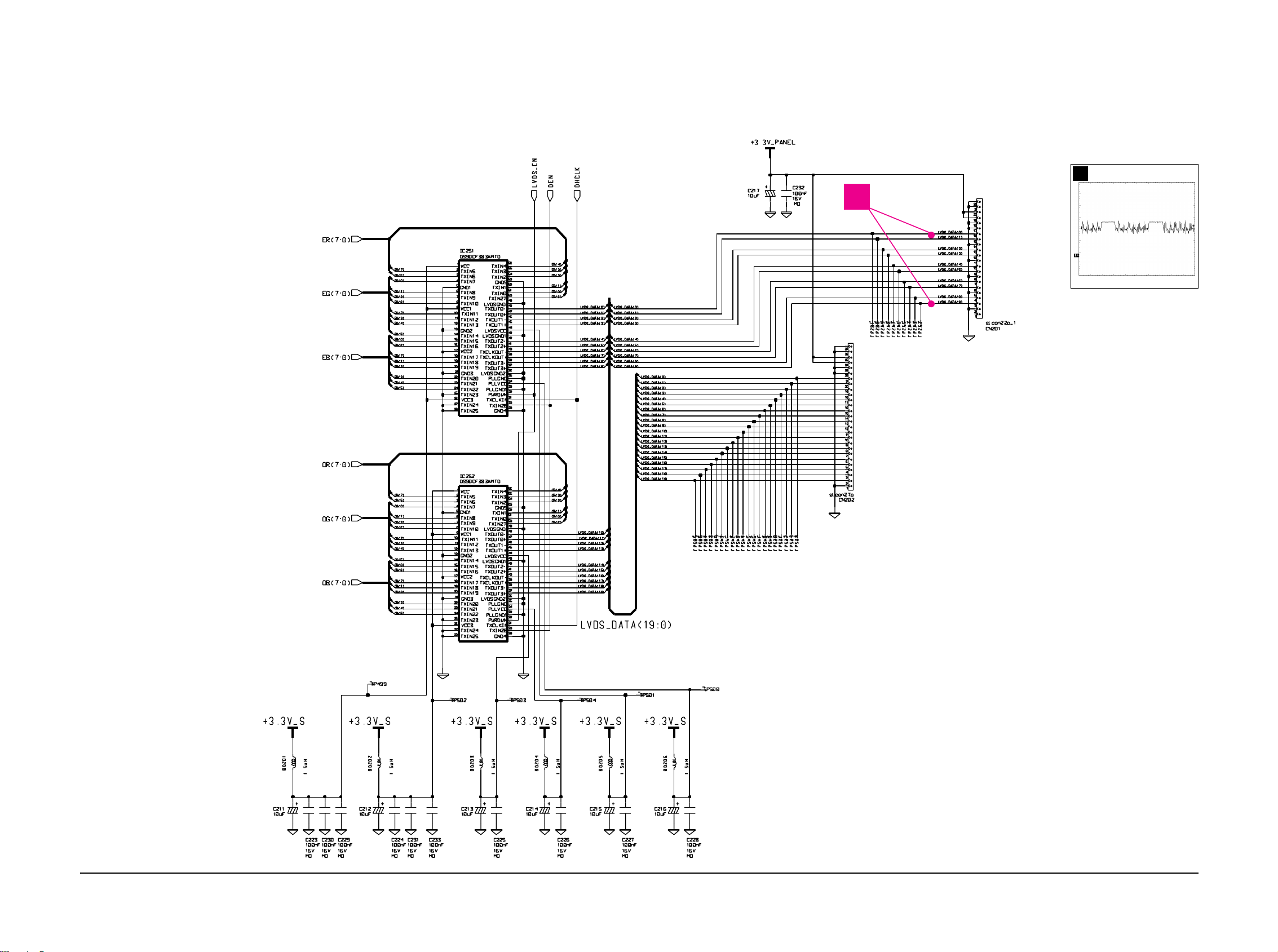
9-2 LVDS Part Schematic diagram
4
4
CN201 #3, 16
CH1 RMS= 1.214V
Page 12
9 Schematic Diagrams
CN15V* 9-3
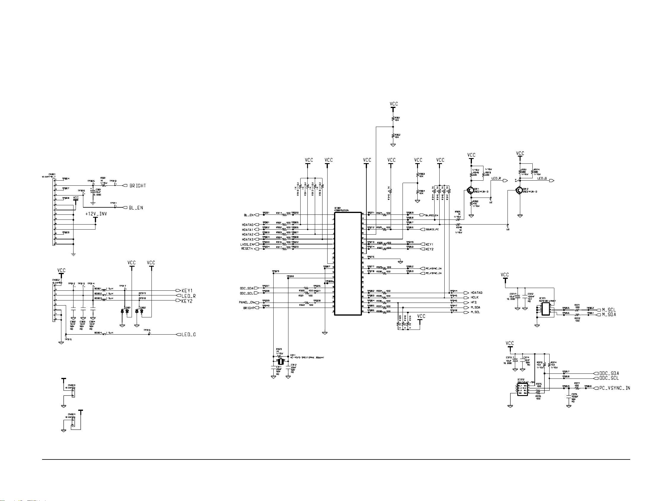
9-3 Micom Part Schematic diagram
+12V_IN
VCC
Page 13

9 Schematic Diagrams
9-4
CN15V*
Memo
Page 14

Memo
8 Wiring Diagram
8-2 CN15V*
Page 15

7 Block Diagrams
7-2 CN15V*
Memo
Page 16
C167 2203-000626 C-CERAMIC,CHIP 0.022nF,5%,50V,NP0,TP,1608
C168 2203-000236 C-CERAMIC,CHIP 0.1nF,5%,50V,NP0,TP,1608
C169 2203-000236 C-CERAMIC,CHIP 0.1nF,5%,50V,NP0,TP,1608
C170 2203-000384 C-CERAMIC,CHIP 0.015nF,5%,50V,NP0,TP,1608
C171 2203-000384 C-CERAMIC,CHIP 0.015nF,5%,50V,NP0,TP,1608
C172 2203-000384 C-CERAMIC,CHIP 0.015nF,5%,50V,NP0,TP,1608
C173 2203-000280 C-CERAMIC,CHIP 0.01nF,0.5pF,50V,NP0,TP,1608
C211 2402-000108 C-AL,SMD 10uF,20%,16V,WT,TP,4.3x4.3x5.4
C215 2402-000108 C-AL,SMD 10uF,20%,16V,WT,TP,4.3x4.3x5.4
C216 2402-000108 C-AL,SMD 10uF,20%,16V,WT,TP,4.3x4.3x5.4
C217 2402-000108 C-AL,SMD 10uF,20%,16V,WT,TP,4.3x4.3x5.4
C223 2203-005005 C-CERAMIC,CHIP 100nF,10%,16V,X7R,TP,1608
C227 2203-005005 C-CERAMIC,CHIP 100nF,10%,16V,X7R,TP,1608
C228 2203-005005 C-CERAMIC,CHIP 100nF,10%,16V,X7R,TP,1608
C229 2203-005005 C-CERAMIC,CHIP 100nF,10%,16V,X7R,TP,1608
C230 2203-005005 C-CERAMIC,CHIP 100nF,10%,16V,X7R,TP,1608
C232 2203-005005 C-CERAMIC,CHIP 100nF,10%,16V,X7R,TP,1608
C301 2402-000108 C-AL,SMD 10uF,20%,16V,WT,TP,4.3x4.3x5.4
C302 2203-000257 C-CERAMIC,CHIP 10nF,10%,50V,X7R,TP,1608
C303 2203-000257 C-CERAMIC,CHIP 10nF,10%,50V,X7R,TP,1608
C304 2203-000257 C-CERAMIC,CHIP 10nF,10%,50V,X7R,TP,1608
C311 2203-000626 C-CERAMIC,CHIP 0.022nF,5%,50V,NP0,TP,1608
C312 2203-000626 C-CERAMIC,CHIP 0.022nF,5%,50V,NP0,TP,1608
C371 2402-000108 C-AL,SMD 10uF,20%,16V,WT,TP,4.3x4.3x5.4
C372 2203-005005 C-CERAMIC,CHIP 100nF,10%,16V,X7R,TP,1608
C373 2402-000108 C-AL,SMD 10uF,20%,16V,WT,TP,4.3x4.3x5.4
C374 2203-000257 C-CERAMIC,CHIP 10nF,10%,50V,X7R,TP,1608
C375 2203-000236 C-CERAMIC,CHIP 0.1nF,5%,50V,NP0,TP,1608
CIS BN41-00069A PCB MAIN CEZANNE-II,FR-4 ,4,-,1.6T,117.0*172.4*1.6,CN,-,-,CL102 BN27-20001A COIL-CHOKE
CN201 3711-003161 CONNECTOR-HEADER BOX,20P,1R,1.25mm,ANGLE,SN SNA
CN301 3711-000556 CONNECTOR-HEADER BOX,12P,1R,1.25mm,SMD-A,SN SNA
CN302 3711-002049 CONNECTOR-HEADER BOX,6P,1R,1.25mm,SMD-A,SN SNA
D101 0402-000553 DIODE-RECTIFIER SS24,40V,2.0A,DO-214AA
D131 0401-001056 DIODE-SWITCHING MMBD4148SE,75V,600mA,SOT-23,TP
D132 0401-001056 DIODE-SWITCHING MMBD4148SE,75V,600mA,SOT-23,TP
D133 0401-001056 DIODE-SWITCHING MMBD4148SE,75V,600mA,SOT-23,TP
D301 0401-001056 DIODE-SWITCHING MMBD4148SE,75V,600mA,SOT-23,TP
D302 0401-001056 DIODE-SWITCHING MMBD4148SE,75V,600mA,SOT-23,TP
FT101 3301-001145 CORE-FERRITE BEAD AB,4.5x1.6x1.6mm,-,- SNA
FT110 3301-001145 CORE-FERRITE BEAD AB,4.5x1.6x1.6mm,-,- SNA
FT111 3301-001145 CORE-FERRITE BEAD AB,4.5x1.6x1.6mm,-,- SNA
FT112 3301-001145 CORE-FERRITE BEAD AB,4.5x1.6x1.6mm,-,- SNA
FT113 3301-001145 CORE-FERRITE BEAD AB,4.5x1.6x1.6mm,-,- SNA
FT114 3301-001145 CORE-FERRITE BEAD AB,4.5x1.6x1.6mm,-,- SNA
FT115 3301-001145 CORE-FERRITE BEAD AB,4.5x1.6x1.6mm,-,- SNA
FT116 3301-001145 CORE-FERRITE BEAD AB,4.5x1.6x1.6mm,-,- SNA
IC102 1203-001488 IC-POSI.FIXED REG. 7805,T0-252,3P,-,PLASTIC,4.8/5
IC104 1203-001447 IC-POSI.FIXED REG. 2596,TO-263,5P,-,PLASTIC,3.135
IC105 1003-001377 IC-LCD CONTROLLER GMZAN1,QFP,160P,1102MIL,SINGLE,-,TR,PLASTIC,3.47V,0TO+70C,1.8W,-,LCD CONTROLLER
IC251 1205-001740 IC-TRANSMITTER DS90C385,TSSOP,56P,240MIL,PLASTIC,4V,1.63W,-10 TO +70C,ST,FPD LINK-85MHZ(LVDS)
IC371 1103-001023 IC-EEPROM 524C80D81,1028x8Bit,SOP,8P,150MIL,10mS,5V,10%,PLASTIC,0to+70C,110uA,CMOS,TP
IC372 1103-001164 IC-EEPROM 24LC21A,128X8BIT,SOP,8P,150MIL,-,5V,10%,PLASTIC,0 TO +70C,100UA,CMOS,TP
Q102 0501-002080 TR-SMALL SIGNAL 2SC2412K,NPN,200mW,SC-59,TP,120-270
Q103 0501-002080 TR-SMALL SIGNAL 2SC2412K,NPN,200mW,SC-59,TP,120-270
Q311 0501-002080 TR-SMALL SIGNAL 2SC2412K,NPN,200mW,SC-59,TP,120-270
Q312 0501-002080 TR-SMALL SIGNAL 2SC2412K,NPN,200mW,SC-59,TP,120-270
R102 2007-000090 R-CHIP 10Kohm,5%,1/16W,DA,TP,1608
R104 2007-000102 R-CHIP 100Kohm,5%,1/16W,DA,TP,1608
R105 2007-000102 R-CHIP 100Kohm,5%,1/16W,DA,TP,1608
R106 2007-000102 R-CHIP 100Kohm,5%,1/16W,DA,TP,1608
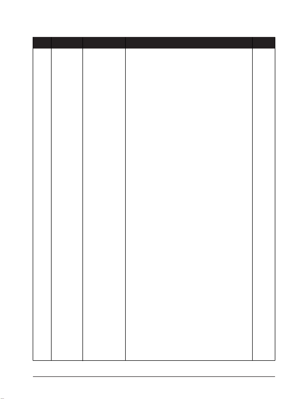
6 Electrical Parts List
6-2 CN15V*
Loc. No. Code No. Description Specification Remarks
Page 17
6 Electrical Parts List
CN15V* 6-3
R107 2007-000090 R-CHIP 10Kohm,5%,1/16W,DA,TP,1608
R108 2007-000084 R-CHIP 4.7Kohm,5%,1/16W,DA,TP,1608
R113 2007-001167 R-CHIP 75ohm,5%,1/16W,DA,TP,1608
R114 2007-000074 R-CHIP 100ohm,5%,1/16W,DA,TP,1608
R115 2007-001167 R-CHIP 75ohm,5%,1/16W,DA,TP,1608
R117 2007-000074 R-CHIP 100ohm,5%,1/16W,DA,TP,1608
R118 2007-000074 R-CHIP 100ohm,5%,1/16W,DA,TP,1608
R119 2007-000074 R-CHIP 100ohm,5%,1/16W,DA,TP,1608
R120 2007-000074 R-CHIP 100ohm,5%,1/16W,DA,TP,1608
R121 2007-000074 R-CHIP 100ohm,5%,1/16W,DA,TP,1608
R122 2007-000074 R-CHIP 100ohm,5%,1/16W,DA,TP,1608
R123 2007-001167 R-CHIP 75ohm,5%,1/16W,DA,TP,1608
R124 2007-001167 R-CHIP 75ohm,5%,1/16W,DA,TP,1608
R125 2007-001167 R-CHIP 75ohm,5%,1/16W,DA,TP,1608
R301 2007-000078 R-CHIP 1Kohm,5%,1/16W,DA,TP,1608
R314 2007-000074 R-CHIP 100ohm,5%,1/16W,DA,TP,1608
R316 2007-000074 R-CHIP 100ohm,5%,1/16W,DA,TP,1608
R317 2007-000074 R-CHIP 100ohm,5%,1/16W,DA,TP,1608
R320 2007-000074 R-CHIP 100ohm,5%,1/16W,DA,TP,1608
R321 2007-000074 R-CHIP 100ohm,5%,1/16W,DA,TP,1608
R322 2007-000074 R-CHIP 100ohm,5%,1/16W,DA,TP,1608
R323 2007-000109 R-CHIP 1Mohm,5%,1/16W,DA,TP,1608
R324 2007-000074 R-CHIP 100ohm,5%,1/16W,DA,TP,1608
R325 2007-000074 R-CHIP 100ohm,5%,1/16W,DA,TP,1608
R326 2007-000074 R-CHIP 100ohm,5%,1/16W,DA,TP,1608
R327 2007-000074 R-CHIP 100ohm,5%,1/16W,DA,TP,1608
R329 2007-000074 R-CHIP 100ohm,5%,1/16W,DA,TP,1608
R330 2007-000074 R-CHIP 100ohm,5%,1/16W,DA,TP,1608
R335 2007-000074 R-CHIP 100ohm,5%,1/16W,DA,TP,1608
R336 2007-000074 R-CHIP 100ohm,5%,1/16W,DA,TP,1608
R337 2007-000074 R-CHIP 100ohm,5%,1/16W,DA,TP,1608
R338 2007-000074 R-CHIP 100ohm,5%,1/16W,DA,TP,1608
R339 2007-000084 R-CHIP 4.7Kohm,5%,1/16W,DA,TP,1608
R340 2007-000084 R-CHIP 4.7Kohm,5%,1/16W,DA,TP,1608
R341 2007-000084 R-CHIP 4.7Kohm,5%,1/16W,DA,TP,1608
R343 2007-000084 R-CHIP 4.7Kohm,5%,1/16W,DA,TP,1608
R344 2007-000084 R-CHIP 4.7Kohm,5%,1/16W,DA,TP,1608
R345 2007-000084 R-CHIP 4.7Kohm,5%,1/16W,DA,TP,1608
R346 2007-000084 R-CHIP 4.7Kohm,5%,1/16W,DA,TP,1608
R348 2007-000078 R-CHIP 1Kohm,5%,1/16W,DA,TP,1608
R349 2007-000075 R-CHIP 220ohm,5%,1/16W,DA,TP,1608
R350 2007-000077 R-CHIP 470ohm,5%,1/16W,DA,TP,1608
R351 2007-000120 R-CHIP 680ohm,5%,1/16W,DA,TP,1608
R362 2007-000090 R-CHIP 10Kohm,5%,1/16W,DA,TP,1608
R364 2007-000090 R-CHIP 10Kohm,5%,1/16W,DA,TP,1608
R371 2007-000074 R-CHIP 100ohm,5%,1/16W,DA,TP,1608
R372 2007-000074 R-CHIP 100ohm,5%,1/16W,DA,TP,1608
R373 2007-000092 R-CHIP 15Kohm,5%,1/16W,DA,TP,1608
R374 2007-000092 R-CHIP 15Kohm,5%,1/16W,DA,TP,1608
R375 2007-000074 R-CHIP 100ohm,5%,1/16W,DA,TP,1608
R376 2007-000074 R-CHIP 100ohm,5%,1/16W,DA,TP,1608
R377 2007-000074 R-CHIP 100ohm,5%,1/16W,DA,TP,1608
R901 2007-000074 R-CHIP 100ohm,5%,1/16W,DA,TP,1608
R902 2007-000074 R-CHIP 100ohm,5%,1/16W,DA,TP,1608
R903 2007-000074 R-CHIP 100ohm,5%,1/16W,DA,TP,1608
R904 2007-000074 R-CHIP 100ohm,5%,1/16W,DA,TP,1608
R905 2007-000078 R-CHIP 1Kohm,5%,1/16W,DA,TP,1608
R910 2007-000078 R-CHIP 1Kohm,5%,1/16W,DA,TP,1608
R911 2007-000078 R-CHIP 1Kohm,5%,1/16W,DA,TP,1608
R912 2007-000078 R-CHIP 1Kohm,5%,1/16W,DA,TP,1608
Loc. No. Code No. Description Specification Remarks
Page 18
R913 2007-000078 R-CHIP 1Kohm,5%,1/16W,DA,TP,1608
R973 2007-000075 R-CHIP 220ohm,5%,1/16W,DA,TP,1608
R974 2007-000120 R-CHIP 680ohm,5%,1/16W,DA,TP,1608
R975 2007-000090 R-CHIP 10Kohm,5%,1/16W,DA,TP,1608
R976 2007-000090 R-CHIP 10Kohm,5%,1/16W,DA,TP,1608
RA130 2011-000002 R-NETWORK 22ohm,5%,63mW,L,CHIP,8P,TP
RA131 2011-000002 R-NETWORK 22ohm,5%,63mW,L,CHIP,8P,TP
RA132 2011-000002 R-NETWORK 22ohm,5%,63mW,L,CHIP,8P,TP
RA133 2011-000002 R-NETWORK 22ohm,5%,63mW,L,CHIP,8P,TP
RA134 2011-000002 R-NETWORK 22ohm,5%,63mW,L,CHIP,8P,TP
RA136 2011-000002 R-NETWORK 22ohm,5%,63mW,L,CHIP,8P,TP
RA137 2011-000002 R-NETWORK 22ohm,5%,63mW,L,CHIP,8P,TP
X100 2801-003755 CRYSTAL-SMD 20MHZ,30PPM,28-AAN,20PF,50OHM,TP
X311 2801-003773 CRYSTAL-SMD 12MHZ,30PPM,28-AAN,20PF,50OHM,TP
ZD181 0403-000579 DIODE-ZENER BZX84C5V1,5.1V,5%,200mW,SOT-23
ZD182 0403-000579 DIODE-ZENER BZX84C5V1,5.1V,5%,200mW,SOT-23
ZD183 0403-000579 DIODE-ZENER BZX84C5V1,5.1V,5%,200mW,SOT-23
ZD184 0403-000579 DIODE-ZENER BZX84C5V1,5.1V,5%,200mW,SOT-23
ZD185 0403-000579 DIODE-ZENER BZX84C5V1,5.1V,5%,200mW,SOT-23
6 Electrical Parts List
6-4 CN15V*
Loc. No. Code No. Description Specification Remarks
CIS BN39-00030A CBF-SIGNAL DETACHABLE,1830MM,15P/15P,-,2990,D-SUB-MALE
CIS BN44-00048A INVERTER
CS15MO,SIC251SF,47Khz,11.5~12.5V,1.5mArms,7.0mArms,-,121*30.5*14.0,2LAMP,-,1.4-2
CIS BN41-00069A PCB MAIN CEZANNE-II,FR-4 ,4,-,1.6T,117.0*172.4*1.6,CN,-,-,CIS BH39-10007A CBF POWER CORD DET,250V/6A,H05VV-F,LP-34A/KKP
CN201+PAN BN39-00083A CBF-HARNESS 20P,140MM,-,UL1571,AWG30,DF14-20S-1.25C
CN301+INV BN39-00002A CBF-HARNESS -,60,BLU/WHT,-,26,CIS BN41-00069A PCB MAIN CEZANNE-II,FR-4 ,4,-,1.6T,117.0*172.4*1.6,CN,-,-,-
Loc. No. Code No. Description Specification Remarks
6-2 Others
Page 19
5 Exploded View & Parts List
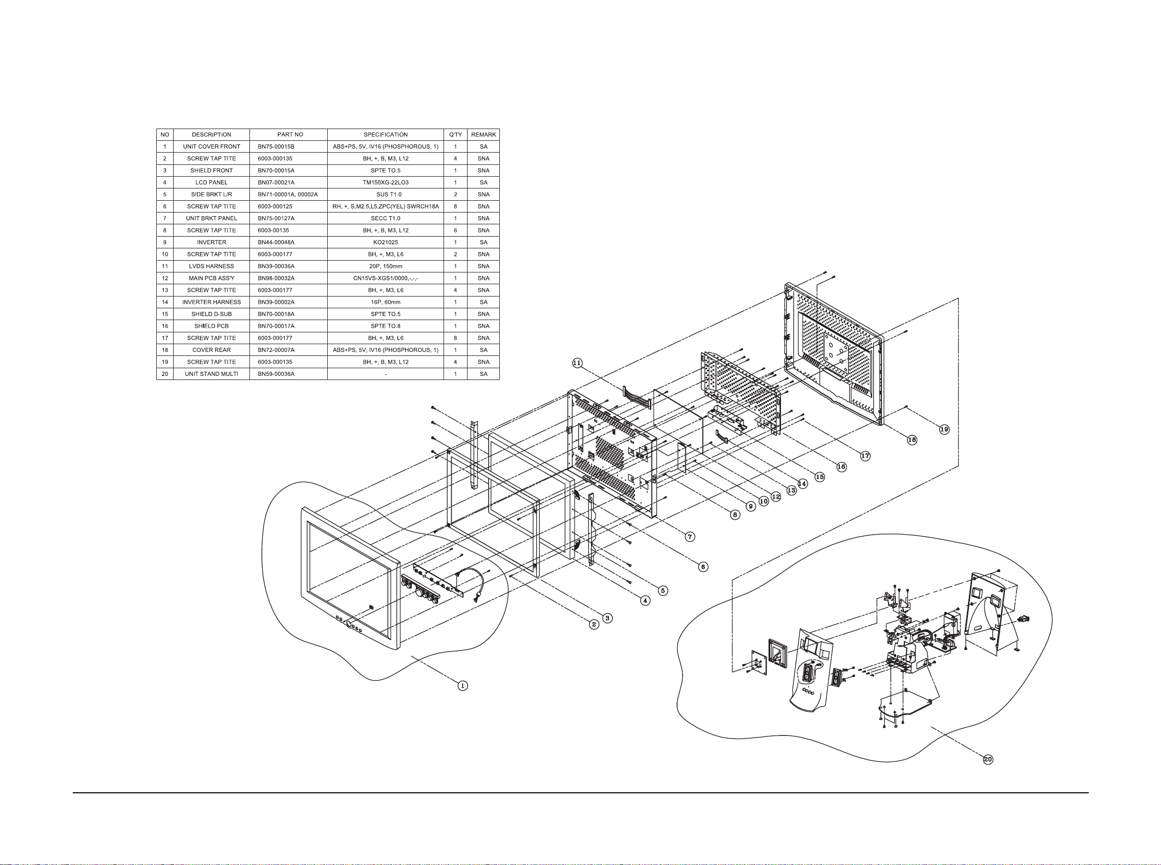
5-2 CN15V*
5-2 Multi Media Base
Page 20
5 Exploded View & Parts List
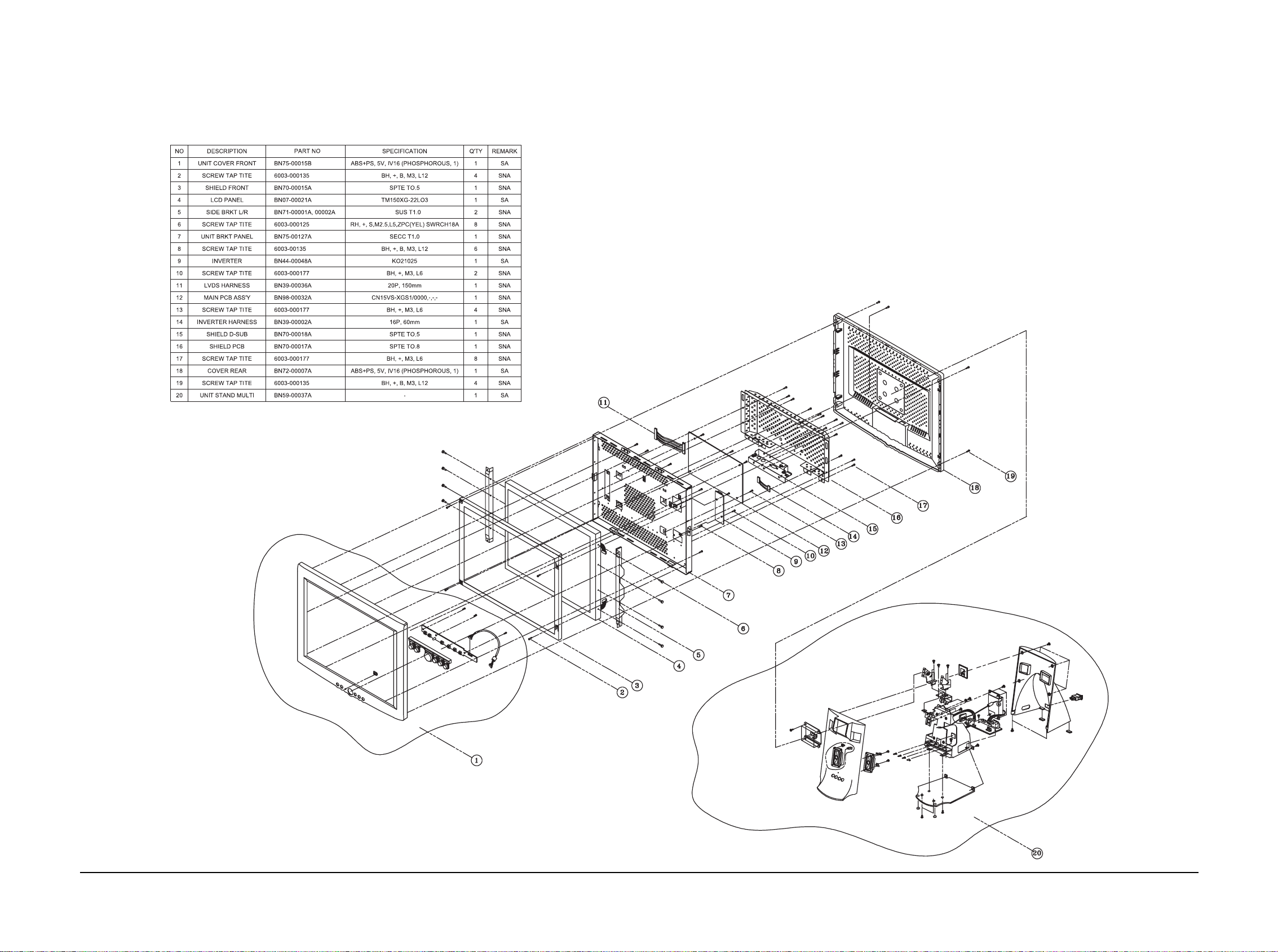
CN15V* 5-3
5-3 Pivot-MultiMedia Base
Page 21
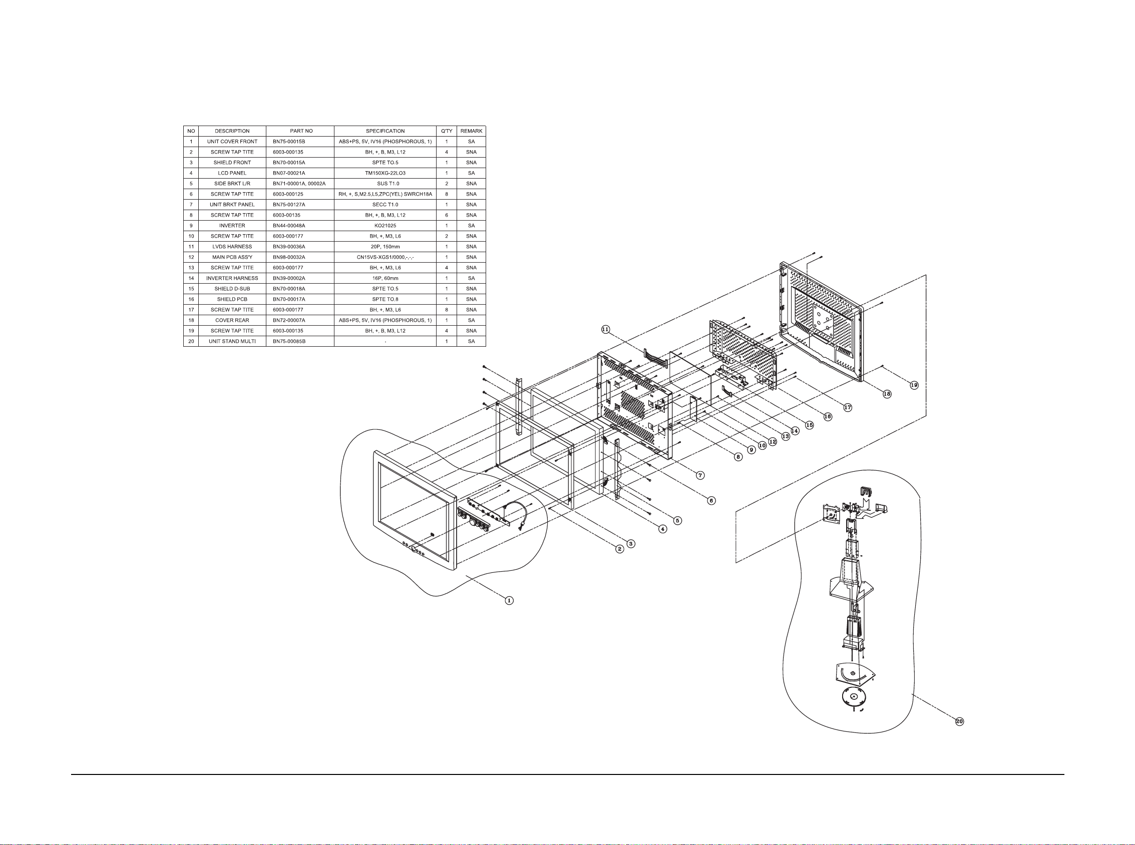
5 Exploded View & Parts List
5-4 CN15V*
5-4 Angle-Pivot Base
Page 22
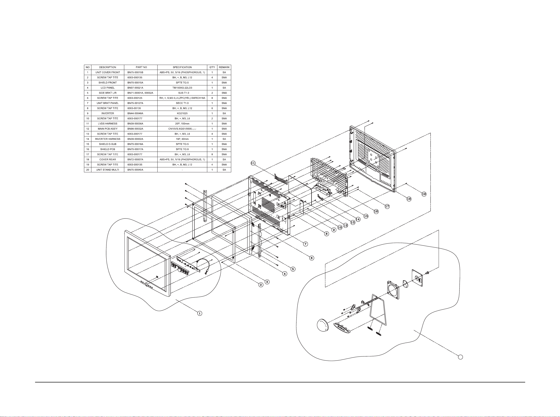
5 Exploded View & Parts List
CN15V* 5-5
5-5 Wire-Frame Base
20
Page 23

5 Exploded View & Parts List
5-6 CN15V*
Memo
Page 24
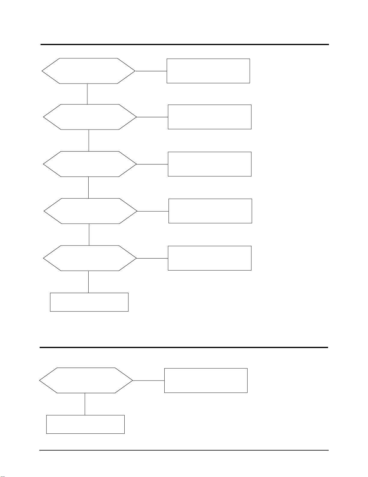
4 Troubleshooting
4-2 CN15V*
4-2 No Video
Replace IC105.
Power indicator is green
Check CN102.
No
Does the clock pulse
appear at Pin 44 of IC105?
Does the H-sync pulse appear
at Pin 150 of IC105?
Replace IC105 or check its
related circuit.
Replace IC251 or check
its related circuit.
No
Do the sync pulses
appear at Pin 43 of IC105?
Yes
Yes
Yes
No
No
3
2
Do the waveforms appeaer at
Pin 3 and 16 of CN201?
4
Replace LCD Panel
Yes
WAVEFORMS
1
1
IC105 #44
CH1 RMS= 1.780V
IC105 #150
CH1 RMS= 3.428V
IC105 #43
CH1 RMS= 4.060V
4
CN201 #3, 16
CH1 RMS= 1.214V
2
3
Page 25
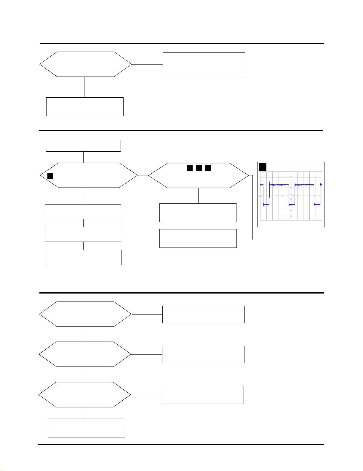
4 Troubleshooting
CN15V* 4-3
4-5 No SOUND
No
Does the DC 12V appear at Pin
2 of IC801 and Pin 6 of CN801?
Check IC801, VR803 and related circuit.
Yes
Check CN805 and CN806 outputs.
No
Does the sound signals appear at
Pin 1 and 3 of IC801?
Check IC801 related circuits.
Yes
No
Does the sound input signal
appear at Pin 6 and 7 of IC801?
Check Pin 1 and 3 of CN801
and related circuits.
Yes
4-3 User Controls Don’t Work
No
Does the DC level change at
Pin 35 and 36 of IC311 when you
push the front panel button?
Check the buttons.
(SW801~SW808)
Yes
Refer to 4-4 No OSD Display.
4-4 No OSD
There is video but no OSD.
While pushing a front control button does
any pulse appear at Pin 46,47
and 55, 56 and 63,64 of IC105?
5
No
Do sync signals appear at Pin 44,
150 and 43 of IC105?
1
Replace IC105.
3
Yes
Replace IC105 or check its
related circuit.
Replace IC105 or check
its related circuit.
2
Replace CN251.
Replace IC251 and IC252.
Yes
No
IC105 #
46,47,55,56,63,64
CH1 RMS= 2.2V
5
Page 26
4-4 CN15V*
4 Troubleshooting
4-6 Microphones Don’t Work
No
Does the PC’s sound
program operate well?
Check the PC’s sound program
and compatibility.
Yes
OK
No
Does the External Microphone
work?
Check the CN803 jack.
Yes
No
Is the connection between the PC
and monitor secure?
Connect the cable between the PC
and monitor.
Yes
OK
No
Can you hear any sound from
the Headphones?
Check CN802 on the Audio PCB
and related circuit D805, D806,
R811, and R812.
Yes
No
Is the Internal Microphone
connector attached?
Check the connection between
CN808 on the Audio PCB and the
Internal Microphone.
Yes
No
Does the Internal Microphone
work?
Check Q801 and related circuits.
Yes
4-7 Headphones Don’t Work
Page 27
4. Remove the Stand Rear from the Stand
assembly.
5. Remove the Stand Front from the Stand
assembly.
6. Remove the Neck Rear from the Stand
assembly.
7. Remove 4 Rubbers on the four corner of the
Stand Bottom and 4 screws on the four corner
of the Stand Bottom.
8. Remove 5 stopper hings from the Bracket
Bottom.
9. Remove the Stand Base from the Stand
Assembly.
3-1-6 Wire frame stand Disassembly (option)
1. Carefully pull the cover hinge.
2. Remove the cover vesa from the Stand
assembly.
3. Remove 4 screws on the assembly Bracket
assembly.
3 Disassembly and Reassembly
3-2 CN15V*
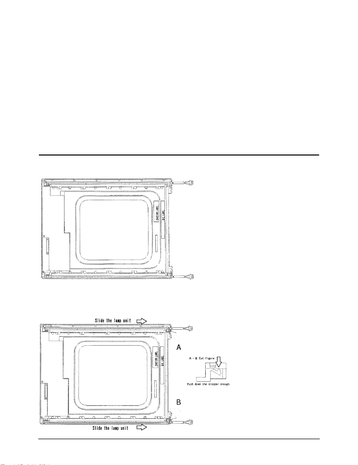
1. After confirm there is nothing
on the disk
Turn the LCD module over
and put it on a flat desk set to
the ground.
3-2 Replacement Order of Lamp Assemblies (CN15VS/CN15VO : Samsung Panel)
(CN15VS/CN15VO : TORISAN Panel)
2. Push down the stopper and
slide the lamp unit.
Page 28
3 Disassembly and Reassembly
CN15V* 3-3
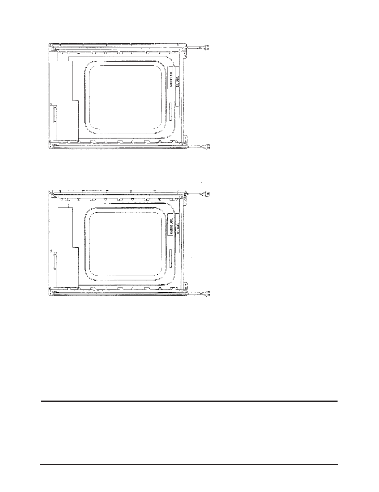
3. Please take out the lamp
unit from the LCD
module.
4. Please fix the new lamp
units on the LCD module :
opposite process 2 and 3
* Replacement of lamp unit should be done at the power off state and recommanded clean
bench condition.
3-3 Reassembly
Reassembly procedures are in the reverse order of Disassembly procedures.
Page 29

Memo
3 Disassembly and Reassembly
3-4 CN15V*
Page 30
2 Product Specifications
2-2 CN15V*
2-2 Pin Assignments
Sync
Type
Pin No.
15-Pin Signal Cable Connector
Separate Composite Sync-on-green
1
2
3
4
5
6
7
8
9
10
11
12
13
14
15
Red
Green
Blue
GND
GND (DDC Return)
GND-R
GND-G
GND-B
No Connection
GND-Sync./Self Test
GND
DDC Data
H-Sync.
V-Sync.
DDC Clock
Red
Green
Blue
GND
GND (DDC Return)
GND-R
GND-G
GND-B
No Connection
GND-Sync./Self Test
GND
DDC Data
H/V-Sync.
Not Used
DDC Clock
Red
Green + H/V Sync.
Blue
GND
GND (DDC Return)
GND-R
GND-G
GND-B
Not Used
GND-Sync./Self Test
GND
DDC Data
Not Used
Not Used
DDC Clock
Page 31
31.469
31.778
3.813
1.589
26.058
0.318
70.086
14.268
0.064
1.716
11.504
0.985
25.175
Positive
Negative
Separate
fH (kHz)
A µsec
B µsec
C µsec
D µsec
E µsec
fV (Hz)
O msec
P msec
Q msec
R msec
S msec
Clock
Frequency
(MHz)
Polarity
H.Sync
V.Sync
Remark
IBM
2 Product Specifications
CN15V* 2-3
QRS
P
O
Video
Sync
Sync
Horizontal
Vertical
CDE
P
O
B
A
Video
Sync
Sync
Separate Sync
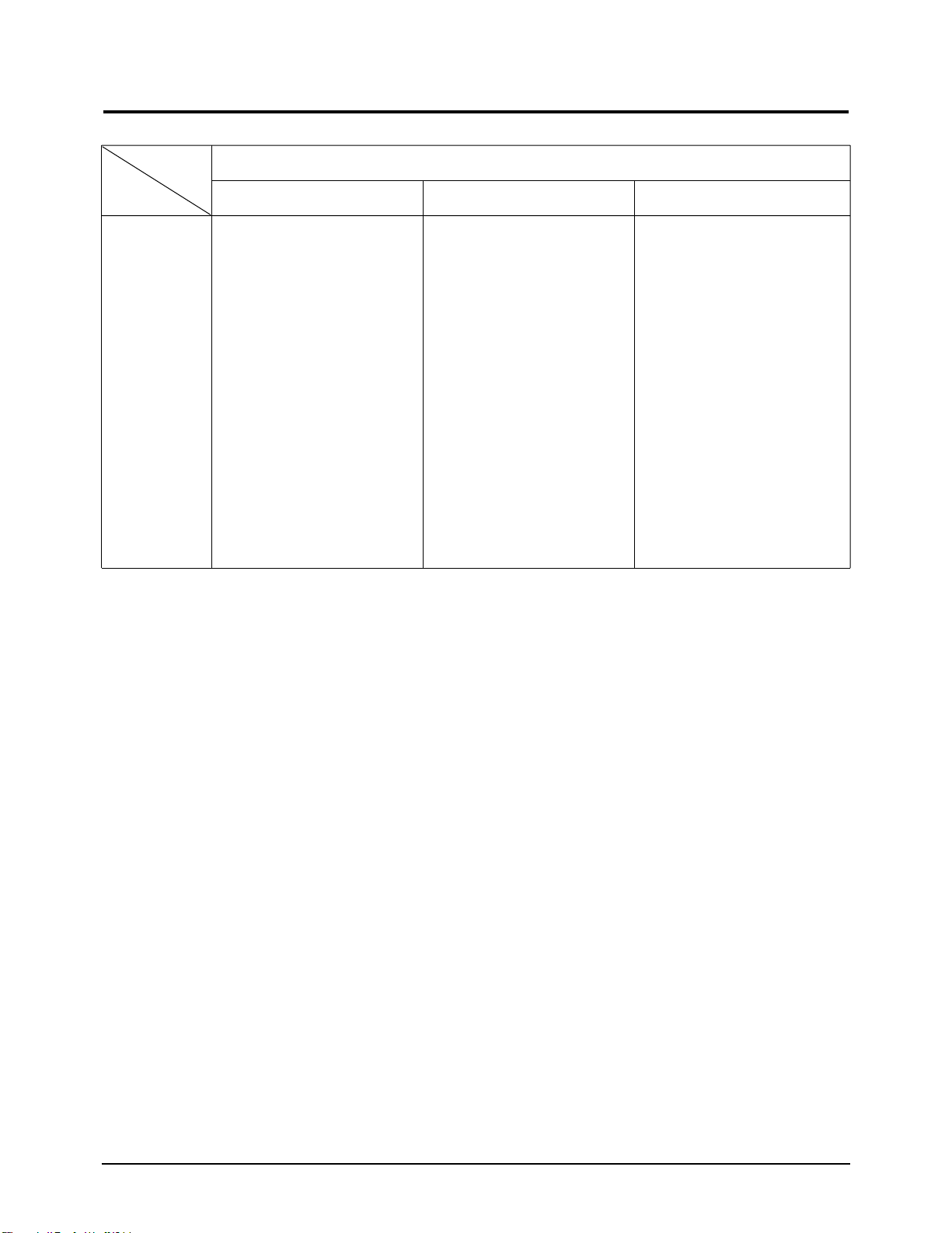
2-3 Timing Chart
This section of the service manual describes the timing that the computer industry recognizes as standard
for computer-generated video signals.
C D
A
O
E
B
P
Video
Sync
Sync
Video
Q R S
A : Line time total B : Horizontal sync width O : Frame time total P : Vertical sync width
C : Back porch D : Active time Q : Back porch R : Active time
E : Front porch S : Front porch
VGA3/60 Hz
640 x 480
640/72 Hz
640 x 480
640/75 Hz
640 x 480
800/56 Hz
800 x 600
800/60 Hz
800 x 600
VGA1/70 Hz
640 x 350
VGA2/70 Hz
720 x 400
Table 2-1. Timing Chart
31.469
31.777
3.813
1.589
26.058
0.318
70.087
14.268
0.064
0.858
13.155
0.191
28.322
Negative
Positive
Separate
31.469
31.778
3.813
1.589
26.058
0.318
59.940
16.683
0.064
0.794
15.761
0.064
25.175
Negative
Negative
Separate
37.861
26.413
1.270
3.810
20.825
0.508
72.809
13.735
0.079
0.528
13.100
0.026
31.500
Negative
Negative
Separate
37.500
26.667
2.032
3.810
20.317
0.508
75.000
13.333
0.080
0.427
12.800
0.027
31.500
Negative
Negative
Separate
35.156
28.444
2.000
3.556
22.222
0.667
56.250
17.778
0.057
0.626
17.067
0.028
36.000
Positive
Negative
Separate
37.879
26.400
3.200
2.200
20.000
1.000
60.317
16.579
0.106
0.607
15.840
0.026
40.000
Positive
Positive
Separate
Mode
VESA
Timing
Page 32
2 Product Specifications
2-4 CN15V*
fH (kHz)
A µsec
B µsec
C µsec
D µsec
E µsec
fV (Hz)
O msec
P msec
Q msec
R msec
S msec
Clock
Frequency
(MHz)
Polarity
H.Sync
V.Sync
Remark
VESA
800/72 Hz
800 x 600
800/75 Hz
800 x 600
640/67 Hz
640 x 480
832/75 Hz
832 x 624
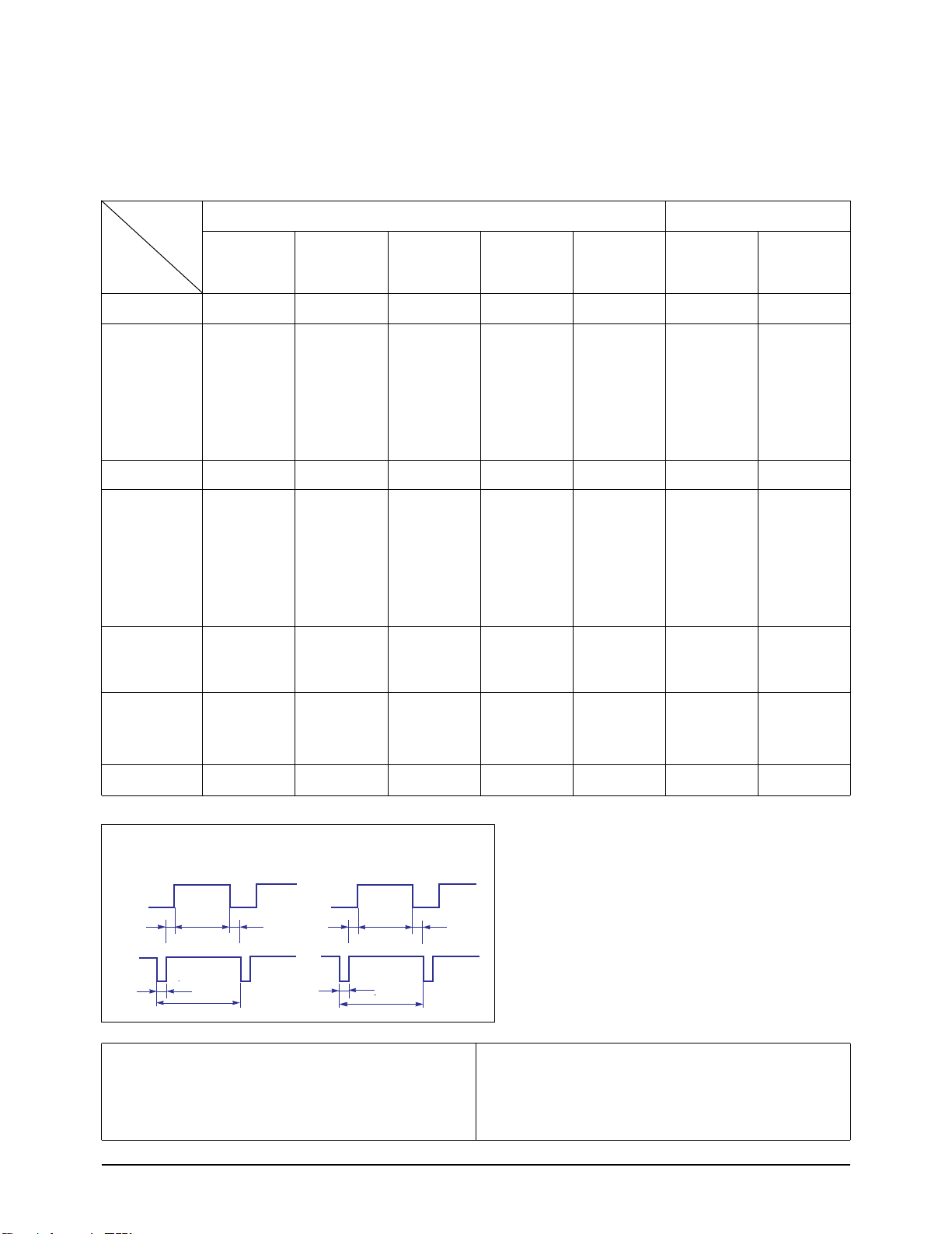
Table 2-1. Timing Chart Continued
48.077
20.800
2.400
1.280
16.000
1.120
72.188
13.853
0.125
0.478
12.480
0.770
50.000
Positive
Positive
Separate
46.875
21.333
1.616
3.232
16.162
0.323
75.000
13.333
0.064
0.448
12.800
0.021
49.500
Positive
Positive
Separate
35.000
28.571
2.116
3.175
21.164
2.116
66.667
15.000
0.086
1.114
13.714
0.086
30.240
Negative
Negative
Separate
49.726
20.110
1.117
3.910
14.524
0.559
74.551
13.414
0.060
0.784
12.549
0.020
57.284
Negative
Negative
Separate
Mode
MAC.
Timing
QRS
P
O
Video
Sync
Sync
Horizontal
Vertical
CDE
P
O
B
A
Video
Sync
Sync
Separate Sync
C D
A
O
E
B
P
Video
Sync
Sync
Video
Q R S
A : Line time total B : Horizontal sync width O : Frame time total P : Vertical sync width
C : Back porch D : Active time Q : Back porch R : Active time
E : Front porch S : Front porch
1024/70Hz
1024x768
56.476
17.707
1.813
1.920
13.653
0.320
70.069
14.272
0.106
0.513
13.599
0.053
75.000
Negative
Negative
Separate
1024/75Hz
1024x768
60.023
16.660
1.219
2.235
13.003
0.203
75.029
13.328
0.050
0.466
12.795
0.017
78.750
Positive
Positive
Separate
1024/60Hz
1024x768
48.363
20.677
2.092
2.462
15.754
0.369
60.004
16.666
0.124
0.600
15.880
0.062
65.000
Negative
Negative
Separate
Page 33

1-2-1 General Servicing Precautions
1. Always unplug the unit’s AC power cord from the
AC power source and disconnect the DC Power
Jack before attempting to:
(a) remove or reinstall any component or assembly,
(b) disconnect PCB plugs or connectors, (c) connect
a test component in parallel with an electrolytic
capacitor.
2. Some components are raised above the printed
circuit board for safety. An insulation tube or tape
is sometimes used. The internal wiring is
sometimes clamped to prevent contact with
thermally hot components. Reinstall all such
elements to their original position.
3. After servicing, always check that the screws,
components and wiring have been correctly
reinstalled. Make sure that the area around the
serviced part has not been damaged.
1. Immediately before handling any semiconductor
components or assemblies, drain the electrostatic
charge from your body by touching a known earth
ground. Alternatively, wear a discharging wriststrap device. To avoid a shock hazard, be sure to
remove the wrist strap before applying power to
the monitor.
2. After removing an ESD-equipped assembly, place it
on a conductive surface such as aluminum foil to
prevent accumulation of an electrostatic charge.
3. Do not use freon-propelled chemicals. These can
generate electrical charges sufficient to damage
ESDs.
4. Use only a grounded-tip soldering iron to solder or
desolder ESDs.
5. Use only an anti-static solder removal device. Some
solder removal devices not classified as “anti-static”
can generate electrical charges sufficient to damage
ESDs.
4. Check the insulation between the blades of the AC
plug and accessible conductive parts (examples:
metal panels, input terminals and earphone jacks).
5. Insulation Checking Procedure: Disconnect the
power cord from the AC source and turn the power
switch ON. Connect an insulation resistance meter
(500 V) to the blades of the AC plug.
The insulation resistance between each blade of the
AC plug and accessible conductive parts (see
above) should be greater than 1 megohm.
6. Always connect a test instrument’s ground lead to
the instrument chassis ground before connecting the
positive lead; always remove the instrument’s
ground lead last.
6. Do not remove a replacement ESD from its
protective package until you are ready to install it.
Most replacement ESDs are packaged with leads
that are electrically shorted together by conductive
foam, aluminum foil or other conductive materials.
7. Immediately before removing the protective
material from the leads of a replacement ESD,
touch the protective material to the chassis or
circuit assembly into which the device will be
installed.
Caution: Be sure no power is applied to the
chassis or circuit and observe all
other safety precautions.
8. Minimize body motions when handling
unpackaged replacement ESDs. Motions such as
brushing clothes together, or lifting your foot from
a carpeted floor can generate enough static
electricity to damage an ESD.
1 Precautions
1-2 CN15V*
1-3 Electrostatically Sensitive Devices (ESD) Precautions
Some semiconductor (solid state) devices can be easily damaged by static electricity. Such components are commonly
called Electrostatically Sensitive Devices (ESD). Examples of typical ESD devices are integrated circuits and some fieldeffect transistors. The following techniques will reduce the incidence of component damage caused by static electricity.
1-2 Servicing Precautions
WARNING: An electrolytic capacitor installed with the wrong polarity might explode.
Caution: Before servicing units covered by this service manual, read and follow the Safety Precautions
section of this manual.
Note: If unforeseen circumstances create conflict between the following servicing precautions and any of the
safety precautions, always follow the safety precautions.
Page 34
Samsung Electronics Co.,Ltd.
416, Maetan-3Dong, Paldal-Gu, Suwon City, Kyungki-Do, Korea.
Tel : +82-31-200-7920 Fax : +82-31-200-7802
Printed in Korea
P/N : BN68-00097K-00
http://www.samsungmonitor.com (SyncMaster Worldwide)
http://www.samsung-monitor.com (SyncMaster USA)
http://www.samtron.com (SAMTRON Worldwide)
http://www.sec.co.kr/monitor (Korea)
 Loading...